ICGOO在线商城 > 集成电路(IC) > 接口 - 驱动器,接收器,收发器 > ISL3180EIBZ

 Datasheet下载
- 型号: ISL3180EIBZ
- 制造商: Intersil
- 库位|库存: xxxx|xxxx
- 要求:
| 数量阶梯 | 香港交货 | 国内含税 |
| +xxxx | $xxxx | ¥xxxx |
查看当月历史价格
查看今年历史价格
ISL3180EIBZ产品简介:
ICGOO电子元器件商城为您提供ISL3180EIBZ由Intersil设计生产,在icgoo商城现货销售,并且可以通过原厂、代理商等渠道进行代购。 ISL3180EIBZ价格参考。IntersilISL3180EIBZ封装/规格:接口 - 驱动器,接收器,收发器, 全 收发器 1/1 RS422,RS485 14-SOIC。您可以下载ISL3180EIBZ参考资料、Datasheet数据手册功能说明书,资料中有ISL3180EIBZ 详细功能的应用电路图电压和使用方法及教程。
ISL3180EIBZ 是 Renesas Electronics America Inc. 生产的一款接口驱动器/接收器/收发器,主要用于工业和通信领域的高速数据传输应用。以下是其主要应用场景:

 1. 工业自动化
   - 设备间通信:ISL3180EIBZ 可用于工业现场总线系统中,实现 PLC(可编程逻辑控制器)、传感器、执行器等设备之间的高速数据交换。
   - 运动控制:在伺服驱动器和电机控制器中,该芯片可用于实时数据传输,确保精确的运动控制。
   - 远程监控:支持远距离信号传输,适用于分布式控制系统(DCS)或 SCADA 系统中的数据采集与监控。

 2. 通信基础设施
   - 网络设备:该芯片适用于路由器、交换机和网关等网络设备中的数据接口,提供可靠的信号驱动和接收功能。
   - 光纤通信:在光模块或光电转换器中,ISL3180EIBZ 能够处理高速电信号的驱动和接收,满足高带宽需求。
   - 背板通信:用于服务器或存储系统的背板连接,确保数据在不同模块之间稳定传输。

 3. 汽车电子
   - 车载网络:支持 CAN、LIN 或其他车载总线协议的信号驱动和接收,适用于汽车电子控制单元(ECU)之间的通信。
   - 信息娱乐系统:在音频/视频信号传输中,该芯片可以确保高质量的数据传输,减少噪声干扰。

 4. 医疗设备
   - 诊断仪器:在超声波、CT 或 MRI 设备中,ISL3180EIBZ 可用于高速数据采集和传输,确保图像质量和诊断精度。
   - 患者监护系统:支持心率、血压等生命体征监测设备的数据传输,保证实时性和可靠性。

 5. 消费类电子产品
   - 高清显示:在显示器、电视或投影仪中,该芯片可用于 HDMI、DisplayPort 等接口的信号驱动,支持高分辨率视频传输。
   - 音频设备:在音响系统或耳机放大器中,提供低失真、高保真的音频信号传输。

 6. 航空航天与国防
   - 军工通信:在雷达、卫星通信或导航系统中,ISL3180EIBZ 可用于高可靠性的数据传输,适应极端环境条件。
   - 无人机控制:支持无人机的遥测数据传输和控制信号处理,确保飞行稳定性。

 特性总结
- 高速数据传输能力,支持多种通信协议。
- 优异的抗干扰性能,适合复杂电磁环境。
- 工业级温度范围,适应恶劣工作条件。
- 小型封装设计,节省电路板空间。

总之,ISL3180EIBZ 广泛应用于需要高速、可靠数据传输的场景,能够满足工业、通信、汽车、医疗等多个领域的严格要求。
| 参数 | 数值 |
| 产品目录 | 集成电路 (IC)半导体 |
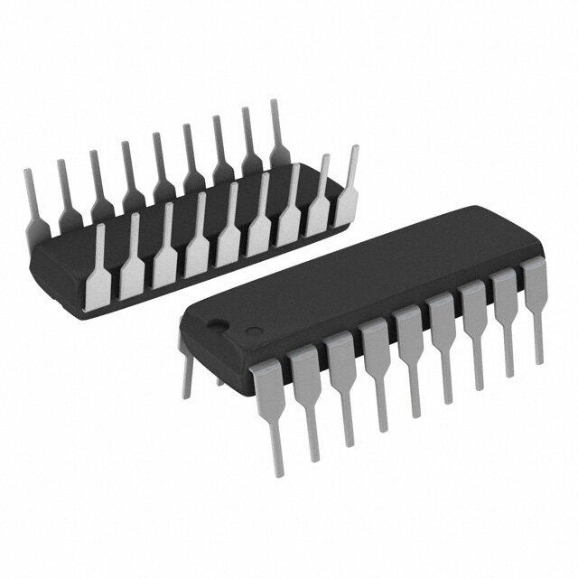
| 描述 | IC TX/RX RS-485/RS-422 14-SOICRS-422/RS-485 接口 IC IEC61000 ESD 14LD 3V RS-485 40MBPS FUL |
| 产品分类 | |
| 品牌 | Intersil |
| 产品手册 | |
| 产品图片 |
|
| rohs | 符合RoHS无铅 / 符合限制有害物质指令(RoHS)规范要求 |
| 产品系列 | 接口 IC,RS-422/RS-485 接口 IC,Intersil ISL3180EIBZ- |
| 数据手册 | |
| 产品型号 | ISL3180EIBZ |
| PCN组件/产地 | |
| 产品培训模块 | http://www.digikey.cn/PTM/IndividualPTM.page?site=cn&lang=zhs&ptm=25593 |
| 产品目录页面 | |
| 产品种类 | RS-422/RS-485 接口 IC |
| 供应商器件封装 | 14-SOICN |
| 关闭 | Yes |
| 功能 | Transceiver |
| 包装 | 管件 |
| 协议 | RS422,RS485 |
| 双工 | 全 |
| 商标 | Intersil |
| 安装类型 | 表面贴装 |
| 安装风格 | SMD/SMT |
| 封装 | Tube |
| 封装/外壳 | 14-SOIC(0.154",3.90mm 宽) |
| 封装/箱体 | SOIC-14 |
| 工作温度 | -40°C ~ 85°C |
| 工作温度范围 | - 40 C to + 85 C |
| 工作电源电压 | 3 V to 3.6 V |
| 工厂包装数量 | 50 |
| 接收器滞后 | 28mV |
| 接收机数量 | 1 Receiver |
| 数据速率 | 40 Mb/s |
| 最大工作温度 | + 85 C |
| 最小工作温度 | - 40 C |
| 标准包装 | 50 |
| 激励器数量 | 1 Driver |
| 电压-电源 | 3 V ~ 3.6 V |
| 电源电流 | 4 mA |
| 类型 | 收发器 |
| 系列 | ISL3180E |
| 输入电压 | - 9 V to + 13 V |
| 输出电压 | - 9 V to + 13 V |
| 驱动器/接收器数 | 1/1 |


- 商务部:美国ITC正式对集成电路等产品启动337调查
- 曝三星4nm工艺存在良率问题 高通将骁龙8 Gen1或转产台积电
- 太阳诱电将投资9.5亿元在常州建新厂生产MLCC 预计2023年完工
- 英特尔发布欧洲新工厂建设计划 深化IDM 2.0 战略
- 台积电先进制程称霸业界 有大客户加持明年业绩稳了
- 达到5530亿美元!SIA预计今年全球半导体销售额将创下新高
- 英特尔拟将自动驾驶子公司Mobileye上市 估值或超500亿美元
- 三星加码芯片和SET,合并消费电子和移动部门,撤换高东真等 CEO
- 三星电子宣布重大人事变动 还合并消费电子和移动部门
- 海关总署:前11个月进口集成电路产品价值2.52万亿元 增长14.8%


PDF Datasheet 数据手册内容提取
DATASHEET ISL3179E, ISL3180E FN6365 High ESD Protected, +125°C, 40Mbps, 3.3V, Full Fail-Safe RS-485/RS-422 Rev. 6.00 Transceivers Nov 9, 2017 The ISL3179E and ISL3180E are high ESD protected (see Features Table2 on page2), 3.3V powered, single transceivers that meet both the RS-485 and RS-422 standards for balanced • High ESD protection on RS-485 I/O pins communication. Each device has low bus currents - ISL3179E. . . . . . . . . . . . . . . . . . . . . . . . . ±16.5kV IEC61000 (+220µA/-150µA), so they present a “1/5 unit load” to the - ISL3180E . . . . . . . . . . . . . . . . . . . . . . . . . . . . . . ±12kV HBM RS-485 bus. This allows up to 160 transceivers on the network - Class 3 HBM level on all other pins (ISL3179E). . . . . >9kV without violating the RS-485 specification’s 32 unit load maximum, and without using repeaters. • Specified for +125°C operation Receiver (Rx) inputs feature a “full fail-safe” design, which • High data rates. . . . . . . . . . . . . . . . . . . . . . . . . . .up to 40Mbps ensures a logic high Rx output if Rx inputs are floating, • 5V tolerant logic inputs shorted, or terminated but undriven. • 1/5 unit load allows up to 160 devices on the bus The ISL3180E is configured for full duplex applications. The • Full fail-safe (open, shorted, terminated/undriven) receiver ISL3179E half duplex version multiplexes the Rx inputs and Tx • Hot plug - Tx and Rx outputs remain three-state during outputs to allow a transceiver with an output disable function power-up in 8 Ld packages. • Low quiescent current. . . . . . . . . . . . . . . . . . . . . . . 4mA (max) Hot plug circuitry ensures that the Tx and Rx outputs remain in a high impedance state while the power supply stabilizes. • Low current shutdown mode . . . . . . . . . . . . . . . . . 1µA (max) • -7V to +12V common-mode input voltage range Related Literature • Three-state Rx and Tx outputs • For a full list of related documents, visit our website • 16/16.5ns (max) Tx/Rx propagation delays; 1.5ns (max) skew - ISL3179E and ISL3180E product pages • Operates from a single +3.3V supply (10% tolerance) Applications • Current limiting and thermal shutdown for driver overload protection • Motor controller/position encoder systems • Pb-free (RoHS compliant) • Factory automation • Field bus networks TABLE 1. KEY DIFFERENCES BETWEEN HIGH-SPEED INTERFACE FAMILY OF PARTS • Security networks PART FULL/HALF VCC VOD DATA RATE • Building environmental control systems NUMBER DUPLEX (V) (V) (Mbps) • Industrial/process control networks ISL3179E Half 3.3 1.5 40 ISL3180E Full 3.3 1.5 40 ISL3159E Half 5 2.1 40 ISL3259E Half 5 2.1 100 +3.3V (SOIC AND MSOP PIN NUMBERS SHOWN) +3.3V + + 0.1µF 0.1µF 8 8 VCC VCC 1 RO R D DI 4 2 RE B/Z 7 RT RT 7 B/Z DE 3 3 DE A/Y 6 6 A/Y RE 2 4 DI RO 1 D R GND GND 5 5 FIGURE 1. TYPICAL OPERATING CIRCUIT - ISL3179E FN6365 Rev. 6.00 Page 1 of 18 Nov 9, 2017
ISL3179E, ISL3180E Ordering Information PART NUMBER PART TEMP. RANGE PACKAGE (Note4, 5) MARKING (°C) (RoHS Compliant) PKG. DWG. # ISL3179EFBZ (Note1) 3179 EFBZ -40 to +125 8 Ld SOIC M8.15 ISL3179EFUZ (Note1) 179FZ -40 to +125 8 Ld MSOP M8.118 ISL3179EFRZ (Note2) 79FZ -40 to +125 10 Ld DFN L10.3x3C ISL3179EIBZ (Note1) 3179 EIBZ -40 to +85 8 Ld SOIC M8.15 ISL3179EIUZ (Note1) 179IZ -40 to +85 8 Ld MSOP M8.118 ISL3179EIRZ (Note2) 79IZ -40 to +85 10 Ld DFN L10.3x3C ISL3180EIBZ (Note3) ISL3180 EIBZ -40 to +85 14 Ld SOIC M14.15 NOTES: 1. Add “-T” suffix for 2.5k unit tape or “-T7A” suffix for 250 unit tape and reel options. Refer to TB347 for details on reel specifications. 2. Add “-T” suffix for 6k unit tape or “-T7A” suffix for 250 unit tape and reel options. Refer to TB347 for details on reel specifications. 3. Add “-T” suffix for 2.5k unit tape and reel options. Refer to TB347 for details on reel specifications. 4. Intersil Pb-free plastic packaged products employ special Pb-free material sets, molding compounds/die attach materials, and 100% matte tin plate plus anneal (e3 termination finish, which is RoHS compliant and compatible with both SnPb and Pb-free soldering operations). Intersil Pb-free products are MSL classified at Pb-free peak reflow temperatures that meet or exceed the Pb-free requirements of IPC/JEDEC J STD-020. 5. For Moisture Sensitivity Level (MSL), refer to the product information page for the ISL3179E and the ISL3180E. For more information about MSL, refer to TB363. TABLE 2. SUMMARY OF FEATURES QUIESCENT PART HALF/FULL DATA RATE RS-485 PIN HOT RX/TX ICC LOW POWER PIN NUMBER DUPLEX (Mbps) ESD LEVEL PLUG? ENABLE? (mA) SHUTDOWN? COUNT ISL3179E HALF 40 16.5kV YES YES 2.6 YES 8, 10 IEC61000 ISL3180E FULL 40 12kV HBM YES YES 2.6 YES 14 FN6365 Rev. 6.00 Page 2 of 18 Nov 9, 2017
ISL3179E, ISL3180E Pin Configurations ISL3179E ISL3179E ISL3180E (8 LD SOIC, MSOP) (10 LD DFN) (14 LD SOIC) TOP VIEW TOP VIEW TOP VIEW RO 1 R 8 VCC RO 1 10 VCC NC 1 14 VCC RE 2 7 B/Z RE 2 9 NC RO 2 13 NC R DE 3 6 A/Y DE 3 EP 8 B/Z RE 3 12 A DI 4 D 5 GND DI 4 7 A/Y DE 4 11 B NC 5 6 GND DI 5 D 10 Z GND 6 9 Y GND 7 8 NC Truth Table Truth Table TRANSMITTING RECEIVING INPUTS OUTPUTS INPUTS OUTPUT RE DE Half DE Full A-B RO RE DE DI B/Z A/Y Duplex Duplex X 1 1 0 1 0 0 X VAB ≥ -0.05V 1 X 1 0 1 0 0 0 X -0.05V > VAB > -0.2V Undetermined 0 0 X High-Z High-Z 0 0 X VAB ≤ -0.2V 0 1 0 X High-Z* High-Z* 0 0 X Inputs Open/Shorted 1 NOTE: *Shutdown Mode 1 0 X X High-Z* 1 1 X X High-Z NOTE: *Shutdown Mode Pin Descriptions PIN FUNCTION RO Receiver output: If A-B ≥ -50mV, RO is high; If A-B ≤ -200mV, RO is low; If A and B are unconnected (floating) or shorted, or connected to a terminated bus that is undriven, RO is high. RE Receiver output enable. RO is enabled when RE is low; RO is high impedance when RE is high. If the Rx enable function isn’t required, connect RE directly to GND. DE Driver output enable. The driver outputs, Y and Z, are enabled by bringing DE high, and they are high impedance when DE is low. If the Tx enable function is not required, connect DE to VCC through a 1kΩ or greater resistor. DI Driver input. A low on DI forces output Y low and output Z high. Similarly, a high on DI forces output Y high and output Z low. GND Ground connection. This is also the potential of the DFN’s exposed metal pad. A/Y ±16.5kV IEC61000 ESD protected RS-485/RS-422 level, noninverting receiver input and noninverting driver output. Pin is an input (A) if DE=0; pin is an output (Y) if DE = 1. ISL3179E only. B/Z ±16.5kV IEC61000 ESD protected RS-485/RS-422 level, inverting receiver input and inverting driver output. Pin is an input (B) if DE = 0; pinis an output (Z) if DE = 1. ISL3179E only. A ±12kV HBM ESD protected RS-485/RS-422 level, noninverting receiver input. ISL3180E only. B ±12kV HBM ESD protected RS-485/RS-422 level, inverting receiver input. ISL3180E only. Y ±12kV HBM ESD protected RS-485/RS-422 level, noninverting driver output. ISL3180E only. Z ±12kV HBM ESD protected RS-485/RS-422 level, inverting driver output. ISL3180E only. VCC System power supply input (3.0V to 3.6V). NC No internal connection. EP The exposed metal pad on the bottom of the DFN; connect to GND. FN6365 Rev. 6.00 Page 3 of 18 Nov 9, 2017
ISL3179E, ISL3180E Typical Operating Circuits (SOIC AND MSOP PIN NUMBERS SHOWN) +3.3V +3.3V + + 0.1µF 0.1µF 8 8 VCC VCC 1 RO R D DI 4 2 RE B/Z 7 RT RT 7 B/Z DE 3 3 DE A/Y 6 6 A/Y RE 2 4 DI RO 1 D R GND GND 5 5 FIGURE 2. ISL3179E (PIN NUMBERS FOR SOIC) +3.3V +3.3V + + 0.1µF 0.1µF 14 14 VCC A 12 RT 9 Y VCC 2 RO DI 5 R B 11 10 Z D 3 RE DE 4 4 DE RE 3 Z 10 RT 11 B 5 DI RO 2 D Y 9 12 A R GND GND 6, 7 6, 7 FIGURE 3. ISL3180E FN6365 Rev. 6.00 Page 4 of 18 Nov 9, 2017
ISL3179E, ISL3180E Absolute Maximum Ratings Thermal Information VCC to Ground . . . . . . . . . . . . . . . . . . . . . . . . . . . . . . . . . . . . . . . . . . . . . . . . 7V Thermal Resistance (Typical) JA (°C/W) JC (°C/W) Input Voltages 8 Ld SOIC Package (Note6) . . . . . . . . . . . . 160 N/A DI, DE, RE. . . . . . . . . . . . . . . . . . . . . . . . . . . . . . . . . . . . . . . . . . . -0.3V to 7V 14 Ld SOIC Package (Note6). . . . . . . . . . . 91 N/A Input/Output Voltages 8 Ld MSOP Package (Note6) . . . . . . . . . . . 132.5 N/A A, B, Y, Z, A/Y, B/Z . . . . . . . . . . . . . . . . . . . . . . . . . . . . . . . . . . -9V to +13V 10 Ld DFN Package (Notes7, 8) . . . . . . . . 46 3.5 RO. . . . . . . . . . . . . . . . . . . . . . . . . . . . . . . . . . . . . . . . . -0.3V to (VCC +0.3V) Maximum Junction Temperature (Plastic Package) . . . . . . . . . . . +150°C Short-circuit Duration Maximum Storage Temperature Range . . . . . . . . . . . . . .-65°C to +150°C Y, Z . . . . . . . . . . . . . . . . . . . . . . . . . . . . . . . . . . . . . . . . . . . . . . . .Continuous Pb-free Reflow Profile . . . . . . . . . . . . . . . . . . . . . . . . . . . . . . Refer to TB493 ESD Rating . . . . . . . . . . . . . . . . . . . . . . Refer to “Electrical Specifications” Operating Conditions Temperature Range ISL3179EF . . . . . . . . . . . . . . . . . . . . . . . . . . . . . . . . . . . .-40°C to +125°C ISL3179EI, ISL3180EI . . . . . . . . . . . . . . . . . . . . . . . . . . . .-40°C to +85°C CAUTION: Do not operate at or near the maximum ratings listed for extended periods of time. Exposure to such conditions may adversely impact product reliability and result in failures not covered by warranty. NOTES: 6. JA is measured with the component mounted on a high-effective thermal conductivity test board in free air. Refer to TB379 for details. 7. For JC, the “case temp” location is the center of the exposed metal pad on the package underside. 8. JA is measured in free air with the component mounted on a high-effective thermal conductivity test board with “direct attach” features. Refer to TB379 for details. Electrical Specifications Test Conditions: VCC = 3.0V to 3.6V; Typicals are at VCC = 3.3V, TA = +25°C. Boldface limits apply across the operating temperature range. (Note9) TEMP MIN MAX PARAMETER SYMBOL TEST CONDITIONS (°C) (Note19) TYP (Note19) UNIT DC CHARACTERISTICS Driver Differential VOUT VOD RL = 100Ω (RS-422) (Figure4A), (Note18) Full 2 2.3 - V RL = 54Ω (RS-485) (Figure4A) Full 1.5 2.1 VCC V No load Full - - VCC RL = 60Ω, -7V ≤VCM ≤12V (Figure4B), (Note18) Full 1.5 2 - V Change in Magnitude of Driver VOD RL = 54Ω or 100Ω (Figure4A) Full - 0.01 0.2 V Differential VOUT for Complementary Output States Driver Common-Mode VOUT VOC RL = 54Ω or 100Ω (Figure4A) Full - 2 2.5 V Change in Magnitude of Driver VOC RL = 54Ω or 100Ω (Figure4A) Full - 0.02 0.2 V Common-Mode VOUT for Complementary Output States Logic Input High Voltage VIH DI, DE, RE Full 2 - - V Logic Input Low Voltage VIL DI, DE, RE Full - - 0.8 V Logic Input Current IIN1 DI = DE = RE = 0V or VCC Full -2 - 2 µA Input Current (A, B, A/Y, B/Z) IIN2 DE = 0V, VCC = 0V or 3.6V VIN = 12V Full - - 220 µA VIN = -7V Full -160 - - µA Y or Z Output Leakage Current IOZ DE = 0V, -7V ≤ VY or VZ ≤ 12V, ISL3180E only Full -40 - 40 µA Driver Short-Circuit Current, IOSD1 DE = VCC, -7V ≤ VY or VZ ≤ 12V (Note11) Full - - ±250 mA VO = High or Low Receiver Differential Threshold VTH -7V ≤ VCM ≤ 12V Full -200 - -50 mV Voltage Receiver Input Hysteresis VTH VCM = 0V 25 - 28 - mV Receiver Output High Voltage VOH IO = -12mA, VID = -50mV Full VCC - 0.5 - - V FN6365 Rev. 6.00 Page 5 of 18 Nov 9, 2017
ISL3179E, ISL3180E Electrical Specifications Test Conditions: VCC = 3.0V to 3.6V; Typicals are at VCC = 3.3V, TA = +25°C. Boldface limits apply across the operating temperature range. (Note9) (Continued) TEMP MIN MAX PARAMETER SYMBOL TEST CONDITIONS (°C) (Note19) TYP (Note19) UNIT Receiver Output Low Voltage VOL IO = +10mA, VID = -200mV Full - - 0.4 V Receiver Output Low Current IOL VOL = 1V, VID = -200mV Full 25 - - mA Three-State (high impedance) IOZR 0.4V ≤ VO ≤ 2.4V Full -1 0.015 1 µA Receiver Output Current Receiver Input Resistance RIN -7V ≤ VCM ≤ 12V Full 54 80 - kΩ Receiver Short-Circuit Current IOSR 0V ≤ VO ≤ VCC Full ±20 - ±110 mA SUPPLY CURRENT No-Load Supply Current (Note10) ICC DI = DE = 0V or VCC Full - 2.6 4 mA Shutdown Supply Current ISHDN DE = 0V, RE = VCC, DI = 0V or VCC Full - 0.05 1 µA ESD PERFORMANCE RS-485 Pins (A/Y, B/Z) IEC61000-4-2, Air-gap Discharge Method 25 - ±16.5 - kV ISL3179E Only IEC61000-4-2, Contact Discharge Method 25 - ±9 - kV Human Body Model, from bus pins to GND 25 - ±16.5 - kV All Pins Human Body Model, per JEDEC 25 - >±9 - kV ISL3179E Only Machine Model, per JEDEC 25 - >±400 - V RS-485 Pins (A, B, Y, Z) IEC61000-4-2, Air-gap Discharge Method 25 - ±4 - kV ISL3180E Only IEC61000-4-2, Contact Discharge Method 25 - ±5 - kV Human Body Model, from bus pins to GND 25 - ±12 - kV All Pins Human Body Model, per JEDEC 25 - ±3 - kV ISL3180E Only Machine Model, per JEDEC 25 - ±150 - V DRIVER SWITCHING CHARACTERISTICS Maximum Data Rate fMAX VOD ≥ ±1.5V, RD = 54Ω, CL = 100pF (Figure7) Full 40 60 - Mbps Driver Differential Output Delay tDD RD = 54Ω, CD = 50pF (Figure5) Full - 11 16 ns Prop Delay Part-to-Part Skew tSKP-P RD = 54Ω, CD = 50pF (Figure5), (Note17) Full - - 4 ns Driver Differential Output Skew tSKEW RD = 54Ω, CD = 50pF (Figure5) Full - 0 1.5 ns Driver Differential Rise or Fall Time tR, tF RD = 54Ω, CD = 50pF (Figure5) Full - 4 7 ns Driver Enable to Output High tZH RL = 110Ω, CL = 50pF, SW = GND (Figure6), Full - 18 25 ns (Note12) Driver Enable to Output Low tZL RL = 110Ω, CL = 50pF, SW = VCC (Figure6), Full - 16 25 ns (Note12) Driver Disable from Output High tHZ RL = 110Ω, CL = 50pF, SW = GND (Figure6) Full - 15 25 ns Driver Disable from Output Low tLZ RL = 110Ω, CL = 50pF, SW = VCC (Figure6) Full - 18 25 ns Time to Shutdown tSHDN (Note14) Full 60 - 600 ns Driver Enable from Shutdown to tZH(SHDN) RL = 110Ω, CL = 50pF, SW = GND (Figure6), Full - - 1000 ns Output High (Notes14, 15) Driver Enable from Shutdown to tZL(SHDN) RL = 110Ω, CL = 50pF, SW = VCC (Figure6), Full - - 1000 ns Output Low (Notes14, 15) RECEIVER SWITCHING CHARACTERISTICS Maximum Data Rate fMAX VID = ±1.5V Full 40 60 - Mbps Receiver Input to Output Delay tPLH, tPHL Figure8 Full - 10 16.5 ns Prop Delay Part-to-Part Skew tSKP-P Figure8, Note17 Full - - 4 ns FN6365 Rev. 6.00 Page 6 of 18 Nov 9, 2017
ISL3179E, ISL3180E Electrical Specifications Test Conditions: VCC = 3.0V to 3.6V; Typicals are at VCC = 3.3V, TA = +25°C. Boldface limits apply across the operating temperature range. (Note9) (Continued) TEMP MIN MAX PARAMETER SYMBOL TEST CONDITIONS (°C) (Note19) TYP (Note19) UNIT Receiver Skew | tPLH - tPHL | tSKD Figure8 Full - 0 1.5 ns Receiver Enable to Output High tZH RL = 1kΩ, CL = 15pF, SW= GND (Figure9), Full - 10 15 ns (Note13) Receiver Enable to Output Low tZL RL = 1kΩ, CL = 15pF, SW= VCC (Figure9), Full - 11 15 ns (Note13) Receiver Disable from Output High tHZ RL = 1kΩ, CL = 15pF, SW= GND (Figure9) Full - 10 15 ns Receiver Disable from Output Low tLZ RL = 1kΩ, CL = 15pF, SW= VCC (Figure9) Full - 10 15 ns Time to Shutdown tSHDN (Note14) Full 60 - 600 ns Receiver Enable from Shutdown to tZH(SHDN) RL = 1kΩ, CL = 15pF, SW = GND (Figure9), Full - - 1000 ns Output High (Notes14, 16) Receiver Enable from Shutdown to tZL(SHDN) RL = 1kΩ, CL = 15pF, SW = VCC (Figure9), Full - - 1000 ns Output Low (Notes14, 16) NOTES: 9. All currents into device pins are positive; all currents out of device pins are negative. All voltages are referenced to device ground unless otherwise specified. 10. Supply current specification is valid for loaded drivers when DE = 0V. 11. Applies to peak current. Refer to “Typical Performance Curves” on page9 for more information. 12. Because of the shutdown feature, keep RE = 0 to prevent the device from entering SHDN. 13. Because of the shutdown feature, the RE signal high time must be short enough (typically <100ns) to prevent the device from entering SHDN. 14. These ICs are put into shutdown by bringing RE high and DE low. If the inputs are in this state for less than 60ns, the parts are guaranteed not to enter shutdown. If the inputs are in this state for at least 700ns, the parts are guaranteed to have entered shutdown. Refer to “Low Power Shutdown Mode” on page13. 15. Keep RE = VCC, and set the DE signal low time >700ns to ensure that the device enters SHDN. 16. Set the RE signal high time >700ns to ensure that the device enters SHDN. 17. This is the part-to-part skew between any two units tested with identical test conditions (Temperature, VCC, etc.). 18. VCC = 3.3V ±5%. 19. Compliance to datasheet limits is assured by one or more methods: production test, characterization, and/or design. Test Circuits and Waveforms RL/2 375Ω VCC DE VCC DE DI Z DI Z VCM D VOD D VOD RL = 60Ω -7V TO +12V Y Y RL/2 VOC 375Ω FIGURE 4A. VOD AND VOC FIGURE 4B. VOD WITH COMMON-MODE LOAD FIGURE 4. DC DRIVER TEST CIRCUITS FN6365 Rev. 6.00 Page 7 of 18 Nov 9, 2017
ISL3179E, ISL3180E Test Circuits and Waveforms (Continued) 3V DI 1.5V 1.5V 0V tPLH tPHL OUT (Z) VOH DE VCC DI Z OUT (Y) VOL D RD CD Y 90% 90% +VOD SIGNAL DIFF OUT (Y - Z) GENERATOR 10% 10% -VOD tR tF SKEW = |tPLH - tPHL| FIGURE 5A. TEST CIRCUIT FIGURE 5B. MEASUREMENT POINTS FIGURE 5. DRIVER PROPAGATION DELAY AND DIFFERENTIAL TRANSITION TIMES DE DI Z 110Ω VCC D 3V SIGNAL Y SW GND DE 1.5V 1.5V GENERATOR 50pF (Note14) 0V tZH, tZH(SHDN) tHZ (Note14) OUTPUT HIGH VOH - 0.5V VOH PARAMETER OUTPUT RE DI SW OUT (Y, Z) 50% tHZ Y/Z X 1/0 GND 0V tLZ Y/Z X 0/1 VCC ttZZHL YY//ZZ 00 ((NNoottee1122)) 10//01 GVNCCD tZL(,N toZtLe(S1H4D)N) tLZ VCC OUT (Y, Z) 50% ttZZHL((SSHHDDNN)) YY//ZZ 11 ((NNoottee1155)) 10//01 GVNCCD OUTPUT LOW VOL + 0.5V VOL FIGURE 6A. TEST CIRCUIT FIGURE 6B. MEASUREMENT POINTS FIGURE 6. DRIVER ENABLE AND DISABLE TIMES DE VCC + 3V DI Z CL DI D 54Ω VOD 0V Y - SIGNAL GENERATOR CL DIFF OUT (Y - Z) +VOD 0V -VOD FIGURE 7A. TEST CIRCUIT FIGURE 7B. MEASUREMENT POINTS FIGURE 7. DRIVER DATA RATE FN6365 Rev. 6.00 Page 8 of 18 Nov 9, 2017
ISL3179E, ISL3180E Test Circuits and Waveforms (Continued) RE +3V 15pF B A 1.5V 1.5V +1.5V RO A R 0V tPLH tPHL SIGNAL VCC GENERATOR RO 1.7V 1.7V 0V FIGURE 8A. TEST CIRCUIT FIGURE 8B. MEASUREMENT POINTS FIGURE 8. RECEIVER PROPAGATION DELAY RE GND AB R RO 1kΩ VCC (Note14) SIGNAL SW GND 3V GENERATOR 15pF RE 1.5V 1.5V 0V tZH, tZH(SHDN) tHZ PARAMETER DE A SW (Note14) OUTPUT HIGH VOH - 0.5V VOH tHZ 0 +1.5V GND RO 1.5V tLZ 0 -1.5V VCC 0V tZH (Note13) 0 +1.5V GND tZL, tZL(SHDN) tLZ (Note14) tZL (Note13) 0 -1.5V VCC VCC tZH(SHDN) (Note16) 0 +1.5V GND RO 1.5V VOL + 0.5V VOL tZL(SHDN) (Note16) 0 -1.5V VCC OUTPUT LOW FIGURE 9A. TEST CIRCUIT FIGURE 9B. MEASUREMENT POINTS FIGURE 9. RECEIVER ENABLE AND DISABLE TIMES Typical Performance Curves VCC = 3.3V, TA = +25°C; unless otherwise specified 90 2.40 80 V) 2.35 T CURRENT (mA) 567000 +125°C+85°C +25°C RDR =D 3=3 5Ω4Ω UTPUT VOLTAGE ( 2222....12235050 RD = 100Ω U 40 O RIVER OUTP 2300 RD = 100Ω FERENTIAL 222...001050 RD = 54Ω D 10 DIF 1.95 0 1.90 0 0.5 1.0 1.5 2.0 2.5 3.0 3.3 -40 -15 10 35 60 85 110 125 DIFFERENTIAL OUTPUT VOLTAGE (V) TEMPERATURE (°C) FIGURE 10. DRIVER OUTPUT CURRENT vs DIFFERENTIAL OUTPUT FIGURE 11. DRIVER DIFFERENTIAL OUTPUT VOLTAGE vs VOLTAGE TEMPERATURE FN6365 Rev. 6.00 Page 9 of 18 Nov 9, 2017
ISL3179E, ISL3180E Typical Performance Curves VCC = 3.3V, TA = +25°C; unless otherwise specified (Continued) 150 2.40 DE = VCC, RE = X OR DE = GND, RE = GND Y OR Z = LOW 2.35 100 A) m 2.30 T ( 50 N A) RE m 2.25 T CUR 0 I (CC U 2.20 P T U O -50 2.15 Y OR Z = HIGH -100 2.10 -7 -6 -4 -2 0 2 4 6 8 10 12 -40 -15 10 35 60 85 110 125 OUTPUT VOLTAGE (V) TEMPERATURE (°C) FIGURE 12. DRIVER OUTPUT CURRENT vs SHORT-CIRCUIT FIGURE 13. SUPPLY CURRENT vs TEMPERATURE VOLTAGE 13.0 0.25 |tPLH - tPHL| 12.5 12.0 0.20 s) n Y ( 11.5 A EL 11.0 s) 0.15 GATION D 1100..05 tPLtHPHL SKEW (n 0.10 A OP 9.5 R P 9.0 0.05 8.5 8.0 0 -40 -15 10 35 60 85 110 125 -40 -15 10 35 60 85 110 125 TEMPERATURE (°C) TEMPERATURE (°C) FIGURE 14. DRIVER DIFFERENTIAL PROPAGATION DELAY vs FIGURE 15. DRIVER DIFFERENTIAL SKEW vs TEMPERATURE TEMPERATURE OUTPUT (V) DI RDIFF = 54Ω, CD = 50pF 05 ER INPUT (V) OUTPUT (V) DI RDIFF = 54Ω, CD = 50pF 05 ER INPUT (V) VER 5 RO DRIV VER 5 RO DRIV EI 0 EI 0 C C E E R R V) 3 V) 3 PUT ( 21 Y-Z PUT ( 12 UT 0 UT 0 O O Y-Z R -1 R -1 E E V -2 V-2 RI RI D -3 D-3 TIME (5ns/DIV) TIME (5ns/DIV) FIGURE 16. DRIVER AND RECEIVER WAVEFORMS FIGURE 17. DRIVER AND RECEIVER WAVEFORMS FN6365 Rev. 6.00 Page 10 of 18 Nov 9, 2017
ISL3179E, ISL3180E Typical Performance Curves VCC = 3.3V, TA = +25°C; unless otherwise specified (Continued) CEIVER OUTPUT (V) 5.00 RDOI = 40Mbps 05DRIVER INPUT (V) CEIVER OUTPUT (V) 5.00 DI = 2RMObps 05DRIVER INPUT (V) RE RE DRIVER+CABLE DELAY (~160ns) DRIVER+CABLE DELAY (~720ns) NPUT (V) 13..50 A - B NPUT (V) 13..50 A - B R I 0 R I 0 CEIVE-1.5 CEIVE-1.5 RE-3.0 RE-3.0 TIME (10ns/DIV) TIME (200ns/DIV) FIGURE 18. DRIVER AND RECEIVER WAVEFORMS DRIVING 100’ FIGURE 19. DRIVER AND RECEIVER WAVEFORMS DRIVING 500’ (31m) OF CAT5 CABLE (DOUBLE TERMINATED WITH (152m) OF CAT5 CABLE (DOUBLE TERMINATED WITH 120Ω) 120Ω) 60 A) VOL +25°C T (m 50 VOH +25°C VOL +85°C N E RR 40 VOL +125°C CU VOH +125°C T U 30 P UT VOH +85°C O R 20 E V EI C E 10 R 0 0 0.5 1.0 1.5 2.0 2.5 3.0 3.3 RECEIVER OUTPUT VOLTAGE (V) FIGURE 20. RECEIVER OUTPUT CURRENT vs RECEIVER OUTPUT VOLTAGE Die Characteristics SUBSTRATE AND DFN THERMAL PAD POTENTIAL (POWERED UP): GND PROCESS: Si Gate BiCMOS FN6365 Rev. 6.00 Page 11 of 18 Nov 9, 2017
ISL3179E, ISL3180E Application Information For parallel applications, bit-to-bit skews between any two transmitter and receiver pairs are guaranteed to be no worse RS-485 and RS-422 are differential (balanced) data than 8ns (4ns max for any two Tx, 4ns max for any two Rx). transmission standards for use in long haul or noisy ESD Protection environments. RS-422 is a subset of RS-485, so RS-485 transceivers are also RS-422 compliant. RS-422 is a All pins on the ISL3179E include Class 3 (>9kV) Human Body point-to-multipoint (multidrop) standard, which allows only one Model (HBM) ESD protection structures, but the RS-485 pins driver and up to 10 receivers on each bus, assuming one unit (driver outputs and receiver inputs) incorporate advanced load devices. RS-485 is a true multipoint standard, which allows structures allowing them to survive ESD events in excess of up to 32 one unit load devices (any mix of drivers and receivers) ±16.5kV HBM (ISL3179E) or ±12kV HBM (ISL3180E), and on each bus. To allow for multipoint operation, the RS-485 ±16.5kV (ISL3179E) or ±4kV (ISL3180E) IEC61000-4-2. The specification requires that drivers must handle bus contention RS-485 pins are particularly vulnerable to ESD strikes because without sustaining any damage. they typically connect to an exposed port on the exterior of the finished product. Simply touching the port pins, or connecting a Another important advantage of RS-485 is the extended cable, can cause an ESD event that can destroy unprotected common-mode range (CMR), which specifies that the driver ICs. These new ESD structures protect the device whether or not outputs and receiver inputs withstand signals that range from it is powered up, and without degrading the RS-485 +12V to -7V. RS-422 and RS-485 are intended for cable lengths as long as 4000ft (~1200m), so the wide CMR is necessary to common-mode range of -7V to +12V. This built-in ESD handle ground potential differences, as well as voltages induced protection eliminates the need for board level protection in the cable by external fields. structures (for example, transient suppression diodes) and the associated, undesirable capacitive load they present. Receiver (Rx) Features IEC61000-4-2 Testing This transceiver utilizes a differential input receiver for maximum noise immunity and common-mode rejection. Input sensitivity is The IEC61000 test method applies to finished equipment, rather ±200mV, as required by the RS-422 and RS-485 specifications. than to an individual IC. Therefore, the pins most likely to suffer Receiver inputs function with common-mode voltages as great an ESD event are those that are exposed to the outside world (the RS-485 pins in this case), and the IC is tested in its typical as +9/-7V outside the power supplies (+12V and -7V), making application configuration (power applied) rather than testing them ideal for long networks, or industrial environments, where each pin-to-pin combination. The IEC61000 standard’s lower induced voltages are a realistic concern. current limiting resistor coupled with the larger charge storage The receiver input resistance of 50kΩ surpasses the RS-422 capacitor yields a test that is much more severe than the HBM specification of 4kΩ, and is five times the RS-485 “Unit Load” test. The extra ESD protection built into the ISL3179E’s RS-485 (UL) requirement of 12kΩ minimum. Thus, the ISL3179E is pins allows the design of equipment meeting Level 4 criteria known as a “one-fifth UL” transceiver, and there can be up to 160 without the need for additional board level protection on the devices on the RS-485 bus while still complying with the RS-485 RS-485 port. loading specification. AIR-GAP DISCHARGE TEST METHOD The receiver is a “full fail-safe” version that guarantees a high level receiver output if the receiver inputs are unconnected For this test method, a charged probe tip moves toward the IC pin (floating), shorted together, or connected to a terminated bus until the voltage arcs to it. The current waveform delivered to the IC pin depends on approach speed, humidity, temperature, etc., with all the transmitters disabled (terminated/undriven). so it is more difficult to obtain repeatable results. The ISL3179E Rx outputs deliver large low state currents (typically 28mA at RS-485 pins withstand ±16.5kV air-gap discharges, while the VOL=1V) to ease the design of optically coupled isolated ISL3180E RS-485 pins withstand ±4kV. networks. CONTACT DISCHARGE TEST METHOD Receivers easily meet the 40Mbps data rate supported by the During the contact discharge test, the probe contacts the tested driver, and the receiver output is tri-statable through the active low RE input. pin before the probe tip is energized, thereby eliminating the variables associated with the air-gap discharge. The result is a Driver (Tx) Features more repeatable and predictable test, but equipment limits prevent testing devices at voltages higher than ±9kV. The RS-485 The RS-485/RS-422 driver is a differential output device that pins of the ISL3179E survive ±9kV contact discharges, while the delivers at least 1.5V across a 54Ω load (RS-485), and at least 2V ISL3180E’s RS-485 pins withstand ±5kV. across a 100Ω load (RS-422). The drivers feature low propagation delay skew to maximize bit width and to minimize Hot Plug Function EMI. When apiece of equipment powers up, a period of time occurs in Driver outputs are not slew rate limited, so faster output which the processor or ASIC driving the RS-485 control lines (DE, transition times allow data rates of at least 40Mbps. Driver RE) is unable to ensure that the RS-485 Tx and Rx outputs are outputs are tri-statable through the active high DE input. kept disabled. If the equipment is connected to the bus, a driver activating prematurely during power-up may crash the bus. To avoid this scenario, the ISL3179E and ISL3180E incorporate a FN6365 Rev. 6.00 Page 12 of 18 Nov 9, 2017
ISL3179E, ISL3180E “hot plug” function. Circuitry monitoring VCC ensures that, during Built-in Driver Overload Protection power-up and power-down, the Tx and Rx outputs remain disabled, As stated previously, the RS-485 specification requires that regardless of the state of DE and RE, if VCC is less than ~2.4V. This drivers survive worst case bus contentions undamaged. These gives the processor/ASIC a chance to stabilize and drive the RS-485 transmitters meet this requirement using driver output short control lines to the proper states. circuit current limits and on-chip thermal shutdown circuitry. The driver output stages incorporate short-circuit current limiting DE, DI = VCC circuitry, which ensures that the output current never exceeds the 2.5V 2.3V RE = GND 24 (V)C RS-485 specification, even at the common-mode voltage range VCC VC extremes. In the event of a major short-circuit condition, the device V) 0 also includes a thermal shutdown feature that disables the drivers T ( whenever the die temperature becomes excessive. This eliminates U 4 P T RL = 1kΩ the power dissipation, allowing the die to cool. The drivers OU 2 automatically reenable after the die temperature drops about ER Y 0 A/Y ISL3179E T (V) +15°C. If the contention persists, the thermal shutdown/reenable V U cycle repeats until the fault is cleared. Receivers stay operational DRI RL = 1kΩ 4 OUTP during thermal shutdown. 2 R RO ISL3179E E Low Power Shutdown Mode 0 EIV C The BiCMOS transceivers use a fraction of the power required by E R their bipolar counterparts, but they also include a shutdown TIME (40µs/DIV) FIGURE 21. HOT PLUG PERFORMANCE (ISL3179E) vs ISL83485 feature that reduces the already low quiescent ICC to a 50nA trickle. The devices enter shutdown whenever the receiver and WITHOUT HOT PLUG CIRCUITRY driver are simultaneously disabled (RE=VCC and DE=GND) for a period of at least 600ns. Disabling both the driver and the Data Rate, Cables, and Terminations receiver for less than 60ns guarantees that the transceiver will RS-485/RS-422 are intended for network lengths up to 4000ft, not enter shutdown. but the maximum system data rate decreases as the Note that receiver and driver enable times increase when the transmission length increases. Devices operating at 40Mbps are transceiver enables from shutdown. Refer to Notes12, 13, 14, limited to lengths less than 100ft. 15 and 16 at the end of “Electrical Specifications” on page5 for Twisted pair is the cable of choice for RS-485/RS-422 networks. more information. Twisted pair cables tend to pick up noise and other electromagnetically induced voltages as common-mode signals, which are effectively rejected by the differential receiver in this IC. Proper termination is imperative to minimize reflections. In point- to-point, or point-to-multipoint (single driver on bus) networks, the main cable should be terminated in its characteristic impedance (typically 120Ω) at the end farthest from the driver. In multireceiver applications, stubs connecting receivers to the main cable should be kept as short as possible. Multipoint (multidriver) systems require that the main cable be terminated in its characteristic impedance at both ends. Stubs connecting a transceiver to the main cable should be kept as short as possible. The ISL3179E and ISL3180E may also be used at slower data rates over longer cables, but some limitations apply. The Rx is optimized for high speed operation, so its output may glitch if the Rx input differential transition times are too slow. Keeping the transition times below 500ns, which equates to the Tx driving a 1000ft (305m) CAT 5 cable, yields excellent performance over the full operating temperature range. FN6365 Rev. 6.00 Page 13 of 18 Nov 9, 2017
ISL3179E, ISL3180E Revision History The revision history provided is for informational purposes only and is believed to be accurate, but not warranted. Please visit our website to make sure you have the latest revision. DATE REVISION CHANGE Nov 9, 2017 FN6365.6 Added the Related Literature section. Updated the Receiving Truth Table on page 3. Updated the header/footer. Aug 25, 2015 FN6365.5 Added Key Differences table to page1. Jul 8, 2015 FN6365.4 Reformatted datasheet to newest template and standards. Features, page1 - Changed: “- Class 3 HBM Level on all Other Pins.....>9kV” to: “- Class 3 HBM level on all other pins (ISL3179E).....>9kV” Pin Description on page3 - Added row for EP pin and added to description of GND. Elec Spec table, page6 ESD Performance section: Added “ISL3179E Only” to All Pins and changed Test Conditions for HBM and Machine Model to “per JEDEC”. - Added 2 rows for “All Pins, ISL3180E Only” Updated note references on Figures 6B and 9B. Die Characteristics section on page11: removed Transistor Count ESD Protection on page 12 - removed “and ISL3180E” from 1st sentence. Added Revision History table and About Intersil section. Updated POD L10.3x3C on page 16 from rev 2 to rev 4. Changes since rev 2: - Removed package outline and included center to center distance between lands on recommended land pattern. - Removed Note 4 "Dimension b applies to the metallized terminal and is measured between 0.18mm and 0.30mm from the terminal tip." since it is not applicable to this package. Renumbered notes accordingly. - Tiebar Note 4 updated From: Tiebar shown (if present) is a non-functional feature. To: Tiebar shown (if present) is a non-functional feature and may be located on any of the 4 sides (or ends). Updated POD M8.15 on page 17 from rev 3 to rev 4. Changes since rev 3: - Changed Note 1 "1982" to "1994" About Intersil Intersil Corporation is a leading provider of innovative power management and precision analog solutions. The company's products address some of the largest markets within the industrial and infrastructure, mobile computing, and high-end consumer markets. For the most updated datasheet, application notes, related documentation, and related parts, see the respective product information page found at www.intersil.com. For a listing of definitions and abbreviations of common terms used in our documents, visit www.intersil.com/glossary. You can report errors or suggestions for improving this datasheet by visiting www.intersil.com/ask. Reliability reports are also available from our website at www.intersil.com/support. © Copyright Intersil Americas LLC 2007-2017. All Rights Reserved. All trademarks and registered trademarks are the property of their respective owners. For additional products, see www.intersil.com/en/products.html Intersil products are manufactured, assembled and tested utilizing ISO9001 quality systems as noted in the quality certifications found at www.intersil.com/en/support/qualandreliability.html Intersil products are sold by description only. Intersil may modify the circuit design and/or specifications of products at any time without notice, provided that such modification does not, in Intersil's sole judgment, affect the form, fit or function of the product. Accordingly, the reader is cautioned to verify that datasheets are current before placing orders. Information furnished by Intersil is believed to be accurate and reliable. However, no responsibility is assumed by Intersil or its subsidiaries for its use; nor for any infringements of patents or other rights of third parties which may result from its use. No license is granted by implication or otherwise under any patent or patent rights of Intersil or its subsidiaries. For information regarding Intersil Corporation and its products, see www.intersil.com FN6365 Rev. 6.00 Page 14 of 18 Nov 9, 2017
ISL3179E, ISL3180E Package Outline Drawing For the most recent package outline drawing, see M8.118. M8.118 8 LEAD MINI SMALL OUTLINE PLASTIC PACKAGE Rev 4, 7/11 5 3.0±0.05 A DETAIL "X" D 8 1.10 MAX SIDE VIEW 2 0.09 - 0.20 4.9±0.15 3.0±0.05 5 0.95 REF PIN# 1 ID 1 2 B 0.65 BSC GAUGE TOP VIEW PLANE 0.25 3°±3° 0.55 ± 0.15 0.85±010 H DETAIL "X" C SEATING PLANE 0.25 - 0.36 0.08MCA-BD 0.10 ± 0.05 0.10C SIDE VIEW 1 (5.80) NOTES: (4.40) (3.00) 1. Dimensions are in millimeters. 2. Dimensioning and tolerancing conform to JEDEC MO-187-AA and AMSEY14.5m-1994. 3. Plastic or metal protrusions of 0.15mm max per side are not included. (0.65) 4. Plastic interlead protrusions of 0.15mm max per side are not (0.40) included. (1.40) 5. Dimensions are measured at Datum Plane "H". 6. Dimensions in ( ) are for reference only. TYPICAL RECOMMENDED LAND PATTERN FN6365 Rev. 6.00 Page 15 of 18 Nov 9, 2017
ISL3179E, ISL3180E Package Outline Drawing For the most recent package outline drawing, see L10.3x3C. L10.3x3C 10 LEAD DUAL FLAT PACKAGE (DFN) Rev 4, 3/15 5 3.00 A PIN #1 INDEX AREA B 10 1 5 2 PIN 1 INDEX AREA 8 3.00 2.3 50 0. 10 x 0.25 6 (4X) 0.10CB 1.64 10x 0.40 TOP VIEW BOTTOM VIEW (4X) 0.10MCB (10 x 0.60) SEE DETAIL "X" (10x 0.25) 0.10C 0.90MAX BASE PLANE C 0.20 SEATING PLANE 38 0.08C 2. SIDE VIEW (8x 0.50) 1.64 2.80 TYP C 0.20 REF 4 TYPICAL RECOMMENDED LAND PATTERN 0.05 DETAIL "X" NOTES: 1. Dimensions are in millimeters. Dimensions in ( ) for Reference Only. 2. Dimensioning and tolerancing conform to AMSE Y14.5m-1994. 3. Unless otherwise specified, tolerance : Decimal ± 0.05 4. Tiebar shown (if present) is a non-functional feature and may be located on any of the 4 sides (or ends). 5. The configuration of the pin #1 identifier is optional, but must be located within the zone indicated. The pin #1 identifier may be either a mold or mark feature. 6. Compliant to JEDEC MO-229-WEED-3 except for E-PAD dimensions. FN6365 Rev. 6.00 Page 16 of 18 Nov 9, 2017
ISL3179E, ISL3180E Package Outline Drawing For the most recent package outline drawing, see M8.15. M8.15 8 LEAD NARROW BODY SMALL OUTLINE PLASTIC PACKAGE Rev 4, 1/12 DETAIL "A" 1.27 (0.050) 0.40 (0.016) INDEX 6.20 (0.244) AREA 5.80 (0.228) 0.50 (0.20) x 45° 4.00 (0.157) 0.25 (0.01) 3.80 (0.150) 8° 1 2 3 0° 0.25 (0.010) 0.19 (0.008) TOP VIEW SIDE VIEW “B” 2.20 (0.087) 1 8 SEATING PLANE 0.60 (0.023) 5.00 (0.197) 1.75 (0.069) 2 7 4.80 (0.189) 1.35 (0.053) 1.27 (0.050) 3 6 -C- 4 5 1.27 (0.050) 0.25(0.010) 0.10(0.004) 0.51(0.020) 5.20(0.205) 0.33(0.013) SIDE VIEW “A TYPICAL RECOMMENDED LAND PATTERN NOTES: 20. Dimensioning and tolerancing per ANSI Y14.5M-1994. 21. Package length does not include mold flash, protrusions or gate burrs. Mold flash, protrusion and gate burrs shall not exceed 0.15mm (0.006 inch) per side. 22. Package width does not include interlead flash or protrusions. Interlead flash and protrusions shall not exceed 0.25mm (0.010 inch) per side. 23. The chamfer on the body is optional. If it is not present, a visual index feature must be located within the crosshatched area. 24. Terminal numbers are shown for reference only. 25. The lead width as measured 0.36mm (0.014 inch) or greater above the seating plane, shall not exceed a maximum value of 0.61mm (0.024 inch). 26. Controlling dimension: MILLIMETER. Converted inch dimensions are not necessarily exact. 27. This outline conforms to JEDEC publication MS-012-AA ISSUE C. FN6365 Rev. 6.00 Page 17 of 18 Nov 9, 2017
ISL3179E, ISL3180E Package Outline Drawing For the most recent package outline drawing, see M14.15. M14.15 14 LEAD NARROW BODY SMALL OUTLINE PLASTIC PACKAGE Rev 1, 10/09 4 0.10CA-B2X 8.65 A 3 6 DETAIL"A" 0.22±0.03 14 8 D 6.0 3.9 4 0.10CD2X PIN NO.1 7 0.20C2X ID MARK (0.35) x 45° 4° ± 4° 5 0.31-0.51 B 3 6 0.25MCA-B D TOP VIEW 0.10C 1.75 MAX H 1.25 MIN 0.25 GAUGE PLANE C 1.27 0.10-0.25 SEATING PLANE 0.10C SIDE VIEW DETAIL "A" (1.27) (0.6) NOTES: 1. Dimensions are in millimeters. Dimensions in ( ) for Reference Only. 2. Dimensioning and tolerancing conform to AMSEY14.5m-1994. 3. Datums A and B to be determined at Datum H. (5.40) 4. Dimension does not include interlead flash or protrusions. Interlead flash or protrusions shall not exceed 0.25mm per side. 5. The pin #1 indentifier may be either a mold or mark feature. 6. Does not include dambar protrusion. Allowable dambar protrusion (1.50) shall be 0.10mm total in excess of lead width at maximum condition. 7. Reference to JEDEC MS-012-AB. TYPICAL RECOMMENDED LAND PATTERN FN6365 Rev. 6.00 Page 18 of 18 Nov 9, 2017