ICGOO在线商城 > 集成电路(IC) > 接口 - 驱动器,接收器,收发器 > LTC1480IS8#TRPBF

 Datasheet下载
- 型号: LTC1480IS8#TRPBF
- 制造商: LINEAR TECHNOLOGY
- 库位|库存: xxxx|xxxx
- 要求:
| 数量阶梯 | 香港交货 | 国内含税 |
| +xxxx | $xxxx | ¥xxxx |
查看当月历史价格
查看今年历史价格
LTC1480IS8#TRPBF产品简介:
ICGOO电子元器件商城为您提供LTC1480IS8#TRPBF由LINEAR TECHNOLOGY设计生产,在icgoo商城现货销售,并且可以通过原厂、代理商等渠道进行代购。 LTC1480IS8#TRPBF价格参考。LINEAR TECHNOLOGYLTC1480IS8#TRPBF封装/规格:接口 - 驱动器,接收器,收发器, 1/1 Transceiver Half RS422, RS485 8-SOIC。您可以下载LTC1480IS8#TRPBF参考资料、Datasheet数据手册功能说明书,资料中有LTC1480IS8#TRPBF 详细功能的应用电路图电压和使用方法及教程。
LTC1480IS8#TRPBF是由Linear Technology(现为Analog Devices旗下品牌)生产的一款低功耗RS-485/RS-422收发器,属于接口类驱动器、接收器、收发器产品。该器件广泛应用于需要可靠串行通信的工业与嵌入式系统中。

其主要应用场景包括工业自动化控制系统,如PLC(可编程逻辑控制器)、远程I/O模块和传感器网络,支持长距离、抗干扰能力强的差分信号传输。在楼宇自动化系统中,如安防监控、门禁控制和环境监测设备,LTC1480IS8#TRPBF可实现稳定的数据收发。此外,它也适用于通信基础设施中的数据终端设备、多点通信网络以及现场总线接口设计。

该芯片采用单一5V供电,具备低静态电流特性,适合对功耗敏感的应用场合。其8引脚SOIC封装节省空间,便于集成到紧凑型电路板中。内置故障安全设计,确保在输入开路或短路时输出保持确定状态,提高了系统可靠性。支持半双工通信模式,符合RS-485标准,最大数据速率可达250kbps,适用于中低速但高稳定性的通信需求。

综上,LTC1480IS8#TRPBF是一款适用于工业、通信及自动化领域中对稳定性、抗干扰能力和低功耗有要求的RS-485通信接口解决方案。
| 参数 | 数值 |
| 产品目录 | 集成电路 (IC) |
| 描述 | IC TXRX 3.3V RS485 LOWPWR 8-SOIC |
| 产品分类 | |
| 品牌 | Linear Technology |
| 数据手册 | http://www.linear.com/docs/3882 |
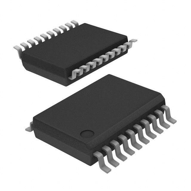
| 产品图片 |
|
| 产品型号 | LTC1480IS8#TRPBF |
| rohs | 无铅 / 符合限制有害物质指令(RoHS)规范要求 |
| 产品系列 | - |
| 供应商器件封装 | 8-SOIC |
| 其它名称 | LTC1480IS8#TRPBFDKR |
| 包装 | Digi-Reel® |
| 协议 | RS422,RS485 |
| 双工 | 半 |
| 安装类型 | 表面贴装 |
| 封装/外壳 | 8-SOIC(0.154",3.90mm 宽) |
| 工作温度 | -40°C ~ 85°C |
| 接收器滞后 | 70mV |
| 数据速率 | 2.5Mbps |
| 标准包装 | 1 |
| 电压-电源 | 3 V ~ 3.6 V |
| 类型 | 收发器 |
| 驱动器/接收器数 | 1/1 |


PDF Datasheet 数据手册内容提取
LTC1480 3.3V Ultralow Power RS485 Transceiver FEATURES DESCRIPTIOU ■ True RS485 from a Single 3.3V Supply The LTC®1480 is an ultralow power differential line trans- ■ Low Power: I = 500µA Max with Driver Disabled ceiver which provides full RS485 compatibility while oper- CC ■ I = 600µA Max with Driver Enabled, No Load ating from a single 3.3V supply. It is designed for data CC ■ 1µA Quiescent in Shutdown Mode transmission standard RS485 applications with extended ■ –7V to 12V Common Mode Range Permits ±7V common mode range (12V to –7V). It also meets the Ground Difference Between Devices on the Data Line requirements of RS422 and features high speed operation ■ Thermal Shutdown Protection up to 2.5Mb/s. The CMOS design offers significant power ■ Power Up/Down Glitch-Free Driver Outputs Permit savings without sacrificing ruggedness against overload Live Insertion or Removal of Transceiver or ESD damage. Typical quiescent current is only 300µA ■ Driver Maintains High Impedance in Three-State or while operating and 1µA in shutdown. with the Power Off The driver and receiver feature three-state outputs, with ■ Up to 32 Transceivers on the Bus the driver outputs maintaining high impedance over the ■ 50ns Typical Driver Propagation Delays with entire common mode range. Excessive power dissipation 10ns Skew caused by bus contention or faults is prevented by a ■ Pin Compatible with the LTC485 thermal shutdown circuit which forces the driver outputs ■ Available in 8-Lead DIP and SO Packages into a high impedance state. The receiver has a fail-safe feature which guarantees a high output state when the APPLICATIOUS inputs are left open. ■ Battery-Powered RS485/RS422 Applications The LTC1480 is fully specified over the commercial and ■ Low Power RS485/RS422 Transceiver extended industrial temperature range. The LTC1480 is ■ Level Translator available in 8-pin SO and DIP packages. , LTC and LT are registered trademarks of Linear Technology Corporation. All other trademarks are the property of their respective owners. TYPICAL APPLICATIOU Driver Differential 3.3V RS485 Network Output Voltage vs Output Current 3.5 3.3V 3.3V LTC1480 LTC1480 VCC = 3.3V 3.0 TA = 25°C RO R SHIELD SHIELD R RO RE B 120Ω 120Ω B RE E (V) 2.5 DE A A DE TAG 2.0 L DI D D DI O 3.3V B A T V 1.5 U P T OU 1.0 0.5 R LTC1480 D 0 0 10 20 30 40 50 60 70 80 90 1480 TA01 OUTPUT CURRENT (mA) RO RE DE DI 1480 TA02 1480fa 1
LTC1480 ABSOLUTE WAXIWUW RATIUGS PACKAGE/ORDER IUFORWATIOU (Note 1) TOP VIEW Supply Voltage (V )................................................ 7V CC Control Input Voltage..................... –0.3V to VCC + 0.3V RO 1 R 8 VCC Driver Input Voltage....................... –0.3V to V + 0.3V RE 2 7 B CC Driver Output Voltage........................................... ±14V DE 3 6 A D DI 4 5 GND Receiver Input Voltage.......................................... ±14V Receiver Output Voltage................ –0.3V to V + 0.3V N8 PACKAGE S8 PACKAGE CC 8-LEAD PDIP 8-LEAD PLASTIC SO Operating Temperature Range TJMAX = 125°C, θJA = 130°C/W (N8) LTC1480C ....................................... 0°C ≤ TA ≤ 70°C TJMAX = 125°C, θJA = 150°C/W (S8) LTC1480I.................................... –40°C ≤ T ≤ 85°C A ORDER PART NUMBER S8 PART MARKING Storage Temperature Range................. –65°C to 150°C LTC1480CN8 1480 Lead Temperature (Soldering, 10 sec)..................300°C LTC1480IN8 1480I LTC1480CS8 LTC1480IS8 Order Options Tape and Reel: Add #TR Lead Free: Add #PBF Lead Free Tape and Reel: Add #TRPBF Lead Free Part Marking: http://www.linear.com/leadfree/ Consult LTC Marketing for parts specified with wider operating temperature ranges. ELECTRICAL CHARACTERISTICS The ● denotes the specifications which apply over the full operating temperature range. V = 3.3V (Notes 2, 3). CC SYMBOL PARAMETER CONDITIONS MIN TYP MAX UNITS V Differential Driver Output Voltage (Unloaded) I = 0V ● 3.3 V OD1 O VOD2 Differential Driver Output Voltage (with Load) R = 27Ω (RS485) (Figure 1) ● 1.5 3.3 V R = 50Ω (RS422) ● 2.0 V ∆VOD Change in Magnitude of Driver Differential Output R = 27Ω or R = 50Ω (Figure 1) ● 0.2 V Voltage for Complementary Output States VOC Driver Common Mode Output Voltage R = 27Ω or R = 50Ω (Figure 1) ● 2 V ∆⏐VOC⏐ Change in Magnitude of Driver Common Mode R = 27Ω or R = 50Ω (Figure 1) ● 0.2 V Output Voltage for Complementary Output States V Input HIGH Voltage DE, DI, RE ● 2 V IH V Input LOW Voltage DE, DI, RE ● 0.8 V IL IIN1 Input Current DE, DI, RE ● ±2 µA I Input Current (A, B) DE = 0, V = 0V or 3.6V, V = 12V ● 1.0 mA IN2 CC IN DE = 0, V = 0V or 3.6V, V = –7V ● –0.8 mA CC IN VTH Differential Input Threshold Voltage for Receiver –7V ≤ VCM ≤ 12V ● –0.2 0.2 V ∆VTH Receiver Input Hysteresis VCM = 0V 70 mV V Receiver Output HIGH Voltage I = –4mA, V = 200mV ● 2 V OH O ID V Receiver Output LOW Voltage I = 4mA, V = –200mV ● 0.4 V OL O ID IOZR Three-State (High Impedance) Output VCC = Max, 0.4V ≤ VO ≤ 2.4V ● ±1 µA Current at Receiver RIN Receiver Input Resistance –7V ≤ VCM ≤ 12V ● 12 kΩ ICC Supply Current No Load, Output Enabled ● 400 600 µA No Load, Output Disabled ● 300 500 µA ISHDN Supply Current in Shutdown Mode DE = 0, RE = VCC 1 10 µA 1480fa 2
LTC1480 SWITCHIU G CHARACTERISTICS The ● denotes the specifications which apply over the full operating temperature range. V = 3.3V (Notes 2, 3). CC SYMBOL PARAMETER CONDITIONS MIN TYP MAX UNITS IOSD1 Driver Short-Circuit Current, VOUT = HIGH –7V ≤ VO ≤ 12V ● 35 250 mA IOSD2 Driver Short-Circuit Current, VOUT = LOW –7V ≤ VO ≤ 12V ● 35 250 mA IOSR Receiver Short-Circuit Current 0V ≤ VO ≤ VCC ● 7 85 mA tPLH Driver Input to Output RDIFF = 54Ω, CL1 = CL2 = 100pF, ● 25 50 80 ns (Figures 3, 5) t Driver Input to Output ● 25 50 80 ns PHL t Driver Output to Output ● 10 20 ns SKEW t , t Driver Rise or Fall Time ● 5 15 40 ns R F t Driver Enable to Output HIGH C = 100pF (Figures 4, 6), S2 Closed ● 70 120 ns ZH L t Driver Enable to Output LOW C = 100pF (Figures 4, 6), S1 Closed ● 70 120 ns ZL L t Driver Disable Time from LOW C = 15pF (Figures 4, 6), S1 Closed ● 70 120 ns LZ L t Driver Disable Time from HIGH C = 15pF (Figures 4, 6), S2 Closed ● 70 120 ns HZ L tPLH Receiver Input to Output RDIFF = 54Ω, CL1 = CL2 = 100pF, ● 30 140 200 ns (Figures 3, 7) t Receiver Input to Output ● 30 140 200 ns PHL tSKD ⏐tPLH – tPHL⏐ Differential Receiver Skew 13 ns t Receiver Enable to Output LOW C = 15pF (Figures 2, 8), S1 Closed ● 50 80 ns ZL RL t Receiver Enable to Output HIGH C = 15pF (Figures 2, 8), S2 Closed ● 50 80 ns ZH RL t Receiver Disable from LOW C = 15pF (Figures 2, 8), S1 Closed ● 50 80 ns LZ RL t Receiver Disable from HIGH C = 15pF (Figures 2, 8), S2 Closed ● 50 80 ns HZ RL f Maximum Data Rate ● 2.5 Mbits/s MAX t Time to Shutdown DE = 0, RE = ● 50 200 600 ns SHDN t Driver Enable from Shutdown to Output HIGH C = 100pF (Figures 4, 6), S2 Closed ● 70 120 ns ZH(SHDN) L t Driver Enable from Shutdown to Output LOW C = 100pF (Figures 4, 6), S1 Closed ● 70 120 ns ZL(SHDN) L t Receiver Enable from Shutdown to Output HIGH C = 15pF (Figures 2, 8), S2 Closed ● 4500 ns ZH(SHDN) L t Receiver Enable from Shutdown to Output LOW C = 15pF (Figures 2, 8), S1 Closed ● 4500 ns ZL(SHDN) L Note 1: Absolute maximum ratings are those beyond which the safety of Note 2: All currents into device pins are positive; all currents out ot device pins the device cannot be guaranteed. are negative. All voltages are referenced to device ground unless otherwise specified. Note 3: All typicals are given for VCC = 3.3V and TA = 25°C. TYPICAL PERFORW AU CE CHARACTERISTICS Driver Output Low/High Voltage Driver Differential Output Voltage Supply Current vs Temperature vs Output Current vs Temperature 425 150 2.2 VCC = 3.3V 400 THERMAL SHUTDOWN 100 TA = 25°C 2.1 RL = 100Ω SUPPLY CURRENT (A)µ233233702557505005 DWRIIVTEHR D DRIISVAEBRL EENDABLED OUTPUT CURRENT (mA) –55000 DIFFERENTIAL VOLTAGE (V) 1112....9870 RL = 54Ω –100 1.6 225 VCC = 3.3V VCC = 3.3V 200 –150 1.5 –50 –25 0 25 50 75 100 125 150 175 0 0.5 1.0 1.5 2.0 2.5 3.0 3.5 –40 –20 0 20 40 60 80 100 TEMPERATURE (°C) 1480 G01 OUTPUT VOLTAGE (V) 1480 G02 TEMPERATURE (°C) 1480 G03 1480fa 3
LTC1480 TYPICAL PERFORWMANUCE CHARACTERISTICS Receiver Output Low Voltage Receiver Output High Voltage Driver Skew vs Temperature vs Output Current vs Output Current 7.0 25 –16 VCC = 3.3V VCC = 3.3V VCC = 3.3V 6.5 TA = 25°C –14 TA = 25°C 20 6.0 A) A) –12 m m s) 5.5 ENT ( 15 ENT ( –10 n R R ME ( 5.0 CUR CUR –8 TI T 10 T 4.5 U U –6 P P T T U U 4.0 O O –4 5 3.5 –2 3.0 0 0 –40 –20 0 20 40 60 80 100 0 0.2 0.4 0.6 0.8 1.0 1.2 1.4 1.6 1.8 2.0 3.30 3.05 2.80 2.55 2.30 2.05 1.80 1.55 1.30 TEMPERATURE (°C) OUTPUT VOLTAGE (V) OUTPUT VOLTAGE (V) 1480 G04 1480 G05 1480 G06 Receiver ⏐⏐⏐⏐⏐tPLH – tPHL⏐⏐⏐⏐⏐ Receiver Output Low Voltage Receiver Output High Voltage vs Temperature vs Temperature vs Temperature 12 0.6 3.0 VCC = 3.3V VCC = 3.3V VCC = 3.3V IO = 8mA IO = 8mA 10 0.5 2.8 V) V) 8 E ( 0.4 E ( E (ns) 6 OLTAG 0.3 OLTAG 2.6 M V V TI UT UT 2.4 P P 4 UT 0.2 UT O O 2.2 2 0.1 0 0 2.0 –40 –20 0 20 40 60 80 100 –40 –20 0 20 40 60 80 100 –40 –20 0 20 40 60 80 100 TEMPERATURE (°C) TEMPERATURE (°C) TEMPERATURE (°C) 1480 G07 1480 G08 1480 G09 PIU FUU CTIOU S RO (Pin 1): Receiver Output. If the receiver output is high, the driver outputs will be fed back to the receiver and enabled (RE LOW) and A > B by 200mV, then RO will be the receive output will correspond to the driver input. HIGH. If A < B by 200mV, then RO will be LOW. DI (Pin 4): Driver Input. If the driver outputs are enabled RE (Pin 2): Receiver Output Enable. A LOW enables the (DE HIGH) then a low on DI forces the outputs A LOW and receiver output, RO. A HIGH input forces the receiver B HIGH. A HIGH on DI with the driver outputs enabled will output into a high impedance state. force A HIGH and B LOW. DE (Pin 3): Driver Outputs Enable. A HIGH on DE enables GND (Pin 5): Ground. the driver output. A, B and the chip will function as a line A (Pin 6): Driver Output/Receiver Input. driver. A low input will force the driver outputs into a high impedance state and the chip will function as a line B (Pin 7): Driver Output/Receiver Input. receiver. If RE is high and DE is LOW, the part will enter a V (Pin 8): Positive Supply. 3.0V < V < 3.6V. CC CC low power (1µA) shutdown state. If RE is low and DE is 1480fa 4
LTC1480 FUU CTIOU TABLES LTC1480 Transmitting LTC1480 Receiving INPUTS OUTPUTS INPUTS OUTPUTS RE DE DI B A RE DE A – B RO X 1 1 0 1 0 0 ≥0.2V 1 X 1 0 1 0 0 0 ≤–0.2V 0 0 0 X Z Z 0 0 Inputs Open 1 1 0 X Z* Z* 1 0 X Z* *Shutdown mode *Shutdown mode TEST CIRCUITS A TEST POINT S1 1k R REOCUETIPVUERT VCC VOD 1k VOC CRL S2 R B 1480 F01 1480 F02 Figure 1. Driver DC Test Load Figure 2. Receiver Timing Test Load 3V DE A A CL1 S1 DI LTC1480 LTC1480 DRIVER B RDIFF CL2 B RECEIVERRE 15RpOF UNDEORU TTPEUSTT 500Ω S2 VCC CL 1480 F03 1480 F04 Figure 3. Driver/Receiver Timing Test Circuit Figure 4. Driver Timing Test Load SWITCHIU G TIW E WAVEFORW S 3V DI 1.5V f = 1MHz, tr ≤ 10ns, tf ≤ 10ns 1.5V 0V tPLH tPHL 1/2 VO B VO A 1/2 VO tSKEW tSKEW VO 90% 90% 0V 10% VDIFF = V(A) – V(B) 10% –VO tr tf 1480 F05 Figure 5. Driver Propagation Delays 1480fa 5
LTC1480 SWITCHIU G TIW E WAVEFORW S 3V DE 1.5V f = 1MHz, tr ≤ 10ns, tf ≤ 10ns 1.5V 0V tZL(SHDN), tZL tLZ 3.3V A, B 2.3V OUTPUT NORMALLY LOW 0.5V VOL A, BVOH 2.3V OUTPUT NORMALLY HIGH 0.5V 0V tZH(SHDN), tZH tHZ 1480 F06 Figure 6. Driver Enable and Disable Times VOH RO 1.5V 1.5V OUTPUT VOL tPHL f = 1MHz, tr ≤ 10ns, tf ≤ 10ns tPLH VOD2 A – B 0V 0V INPUT –VOD2 1480 F07 Figure 7. Receiver Propagation Delays 3V RE 1.5V f = 1MHz, tr ≤ 10ns, tf ≤ 10ns 1.5V 0V tZL(SHDN), tZL tLZ 3.3V RO 1.5V OUTPUT NORMALLY LOW 0.5V VOL ROVOH 1.5V OUTPUT NORMALLY HIGH 0.5V 0V tZH(SHDN), tZH tHZ 1480 F08 Figure 8. Receiver Enable and Disable Times APPLICATIOUS IUFORWATIOU VCC CMOS Output Driver VCC SD3 P1 PP11 The LTC1480 transceiver provides full RS485 compatibility while operating from a single 3.3V supply. The RS485 specification requires that a transceiver withstand common D1 D1 mode voltages of up to 12V or –7V at the RS485 line OUTPUT LOGIC OUTPUT LOGIC connections. Additionally, the transceiver must be immune SD4 to both ESD and latch-up. This rules out traditional CMOS N1 D2 N1 D2 drivers, which include parasitic diodes from their driver outputs to each supply rail (Figure 9). The LTC1480 uses a proprietary process enhancement which adds a pair of 1480 F09 1480 F10 Schottky diodes to the output stage (Figure 10), preventing Figure 9. Conventional Figure 10. CMOS Output Stage LTC1480 Output Stage 1480fa 6
LTC1480 APPLICATIOUS IUFORWATIOU current from flowing when the common mode voltage driver outputs enabled but unterminated, quiescent cur- exceeds the supply rails. Latch-up at the output drivers is rent will rise as one of the two outputs sources current into virtually eliminated and the driver is prevented from loading the internal receiver input resistance. With the minimum the line under RS485 specified fault conditions. receiver input resistance of 12k and the maximum output swing of 3.3V, the quiescent current will rise by a maxi- When two or more drivers are connected to the same mum of 275µA. Typical quiescent current rise with the transmission line, a potential condition exists whereby driver enabled is about 100µA. more than two drivers are simultaneously active. If one or more drivers is sourcing current while another driver is The quiescent current rises significantly if the driver is sinking current, excessive power dissipation may occur enabled when it is externally terminated. With 1/2 termina- within either the sourcing or sinking element. This condi- tion load (120Ω between the driver outputs) the quiescent tion is defined as driver contention, since multiple drivers current will jump to at least 13mA as the drivers force a are competing for one transmission line. The LTC1480 minimum of 1.5V across the termination resistance. With provides a current limiting scheme to prevent driver a fully terminated 60Ω line attached, the current will rise contention failure. When driver contention occurs, the to greater than 25mA with the driver enabled, completely current drawn is limited to about 70mA preventing exces- overshadowing the extra 100µA drawn by internal receiver sive power dissipation within the drivers. inputs. The LTC1480 has a thermal shutdown feature which Shutdown Mode protects the part from excessive power dissipation. Under extreme fault conditions, up to 250mA can flow through Both the receiver output (RO) and the driver outputs (A, B) the part causing rapid internal temperature rise. The can be placed in three-state mode by bringing RE HIGH thermal shutdown circuit will disable the driver outputs and DE LOW respectively. In addition, the LTC1480 will when the internal temperature reaches 150°C and turns enter shutdown mode when RE is HIGH and DE is LOW. them back on when the temperature cools to 130°C. This In shutdown the LTC1480 typically draws only 1µA of cycle will repeat as necessary until the fault condition is supply current. In order to guarantee that the part goes removed. into shutdown, RE must be high and DE must be LOW for at least 600ns simultaneously. If this time duration is less Receiver Inputs than 50ns the part will not enter shutdown mode. The LTC1480 features an input common mode range covering the entire RS485 specified range of –7V to 12V. Propagation Delay Differential signals of greater than ±200mV within the Many digital encoding schemes are dependent upon the specified input common mode range will be converted to difference in the propagation delay times of the driver and a TTL compatible signal at the receiver output. A small receiver. Figure 11 shows the test circuit for the LTC1480 amount of input hysteresis is included to minimize the propagation delay. effects of noise on the line signals. If the receiver inputs are The receiver delay times are: floating (unterminated) an internal pull-up of 10µA at the A input will force the receiver output to a known high state. ⏐tPLH – tPHL⏐ = 13ns Typ, VCC = 3.3V The driver’s skew times are: Low Power Operation t = 10ns Typ, V = 3.3V SKEW CC The LTC1480 draws very little supply current whenever the driver outputs are disabled. In shutdown mode the 20ns Max, VCC = 3.3V, TA = –40°C to 85°C quiescent current is typically less than 1µA. With the receiver active and the driver outputs disabled, the LTC1480 will typically draw 300µA quiescent current. With the 1480fa Information furnished by Linear Technology Corporation is believed to be accurate and reliable. 7 However, no responsibility is assumed for its use. Linear Technology Corporation makes no represen- tation that the interconnection of its circuits as described herein will not infringe on existing patent rights.
LTC1480 APPLICATIOUS IUFORWATIOU 100pF BR tr, tfT <T L6 nINs D R R ROEUCTEIVER 100Ω 1480 F11 100pF Figure 11. Receiver Propagation Delay Test Circuit PACKAGE DESCRIPTIOU N8 Package 8-Lead PDIP (Narrow .300 Inch) (Reference LTC DWG # 05-08-1510) .300 – .325 .045 – .065 .130 ± .005 .400* (7.620 – 8.255) (1.143 – 1.651) (3.302 ± 0.127) (10.160) MAX 8 7 6 5 .065 (1.651) .008 – .015 TYP (0.203 – 0.381) .120 .255 ± .015* (3.048) .020 (6.477 ± 0.381) +.035 MIN (0.508) .325–.015 .100 .018 ± .003 MIN (8.255+0.889) (2.54) (0.457 ± 0.076) 1 2 3 4 –0.381 BSC NOTE: INCHES N8 1002 1. DIMENSIONS ARE *THESE DIMENSIONS DO NOT INCLUDE MOLD FLASH OR PROTRUSIONS. MILLIMETERS MOLD FLASH OR PROTRUSIONS SHALL NOT EXCEED .010 INCH (0.254mm) S8 Package 8-Lead Plastic Small Outline (Narrow .150 Inch) (Reference LTC DWG # 05-08-1610) .189 – .197 (4.801 – 5.004) .045 ±.005 NOTE 3 .050 BSC 8 7 6 5 .053 – .069 (1.346 – 1.752) .004 – .010 (0.101 – 0.254) .M24IN5 .160 ±.005 (5..272981 –– .62.41497) (3..185100 –– .31.59788) .014 – .019 .050 NOTE 3 (0.355 – 0.483) (1.270) TYP BSC .010 – .020 × 45°(cid:31) .030 ±.005 (0.254 – 0.508) TYP 1 2 3 4 .008 – .010 RECOMMENDED SOLDER PAD LAYOUT (0.203 – 0.254) 0°– 8° TYP NOTE: INCHES 1. DIMENSIONS IN 3. THESE DIMENSIONS DO NOT INCLUDE MOLD FLASH OR PROTRUSIONS. (MILLIMETERS) MOLD FLASH OR PROTRUSIONS SHALL NOT EXCEED .006" (0.15mm) .016 – .050 2. DRAWING NOT TO SCALE (0.406 – 1.270) SO8 0303 RELATED PARTS PART NUMBER DESCRIPTION COMMENTS LTC485 5V Low Power RS485 Interface Transceiver Low Power LTC1481 5V Ultralow Power RS485 Transceiver with Shutdown Lowest Power LTC1483 5V Ultralow Power RS485 Low EMI Transceiver with Shutdown Low EMI/Lowest Power LTC1485 5V Differential Bus Transceiver High Speed, 10Mbps LTC1487 5V Ultralow Power RS485 with Low EMI, Shutdown High Input Impedance/Low EMI/Lowest Power and High Input Impedance 1480fa 8 Linear Technology Corporation LT/LT 0605 REV A • PRINTED IN USA 1630 McCarthy Blvd., Milpitas, CA 95035-7417 (408) 432-1900 ● FAX: (408) 434-0507 ● www.linear.com © LINEAR TECHNOLOGY CORPORATION 1995
Mouser Electronics Authorized Distributor Click to View Pricing, Inventory, Delivery & Lifecycle Information: A nalog Devices Inc.: LTC1480CS8#PBF LTC1480IN8 LTC1480IS8#PBF LTC1480CN8 LTC1480IS8#TR LTC1480IN8#PBF LTC1480CS8#TR LTC1480CN8#PBF LTC1480IS8#TRPBF LTC1480CS8 LTC1480IS8 LTC1480CS8#TRPBF