ICGOO在线商城 > 集成电路(IC) > 接口 - 驱动器,接收器,收发器 > DS26LV32ATM
 Datasheet下载
- 型号: DS26LV32ATM
- 制造商: Texas Instruments
- 库位|库存: xxxx|xxxx
- 要求:
| 数量阶梯 | 香港交货 | 国内含税 |
| +xxxx | $xxxx | ¥xxxx |
查看当月历史价格
查看今年历史价格
DS26LV32ATM产品简介:
ICGOO电子元器件商城为您提供DS26LV32ATM由Texas Instruments设计生产,在icgoo商城现货销售,并且可以通过原厂、代理商等渠道进行代购。 DS26LV32ATM价格参考¥询价-¥询价。Texas InstrumentsDS26LV32ATM封装/规格:接口 - 驱动器,接收器,收发器, 接收器 0/4 RS422,RS485 16-SOIC。您可以下载DS26LV32ATM参考资料、Datasheet数据手册功能说明书,资料中有DS26LV32ATM 详细功能的应用电路图电压和使用方法及教程。
DS26LV32ATM是Texas Instruments(德州仪器)生产的一款接口驱动器、接收器和收发器,广泛应用于高速数据传输领域。该器件支持低电压差分信号(LVDS)技术,能够在长距离、高噪声环境下实现稳定的数据传输,适用于多种工业、通信及消费电子设备。

 应用场景

1. 通信设备:
   - DS26LV32ATM常用于路由器、交换机等网络设备中,作为高速数据接口,确保不同设备之间的高效通信。其低功耗和高抗噪性使其在复杂的电磁环境中表现出色,适合数据中心、服务器集群等应用。

2. 工业自动化:
   - 在工业控制系统中,如PLC(可编程逻辑控制器)、HMI(人机界面)等,DS26LV32ATM可用于连接传感器、执行器和其他控制模块,提供可靠的数据传输通道。它支持多点通信,能够在一个总线上连接多个设备,简化布线并提高系统集成度。

3. 消费电子产品:
   - 该芯片也可用于高清电视、投影仪、显示器等消费电子产品中,作为视频信号传输的接口。LVDS技术能有效减少电磁干扰,保证图像质量的同时降低功耗,提升用户体验。

4. 医疗设备:
   - 医疗成像设备如CT扫描仪、超声波设备等需要高精度的数据传输,DS26LV32ATM可以确保这些设备内部各模块之间的高速、低延迟通信,从而提高诊断准确性。

5. 汽车电子:
   - 在车载信息系统中,如仪表盘、娱乐系统等,DS26LV32ATM可用于连接显示屏与主控单元,提供稳定的图像和音频传输。其抗干扰能力强,能在复杂的工作环境中保持良好的性能。

 总结

DS26LV32ATM凭借其低功耗、高抗噪性和高速传输特性,在多个领域都有广泛应用。无论是工业自动化、通信设备还是消费电子产品,它都能为用户提供可靠的接口解决方案,满足不同应用场景的需求。
| 参数 | 数值 |
| 产品目录 | 集成电路 (IC)半导体 |
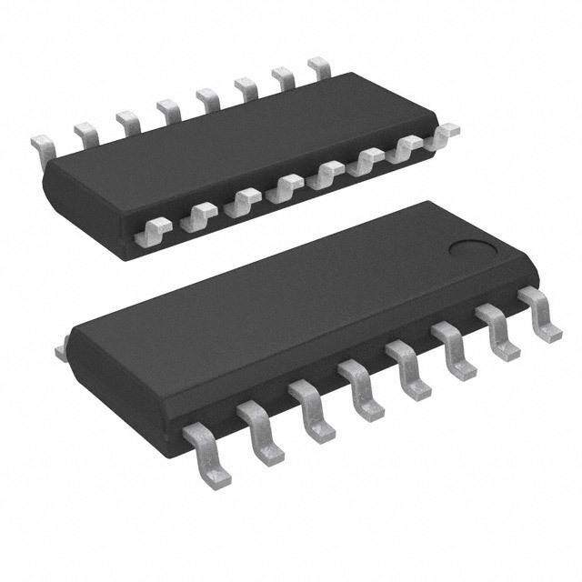
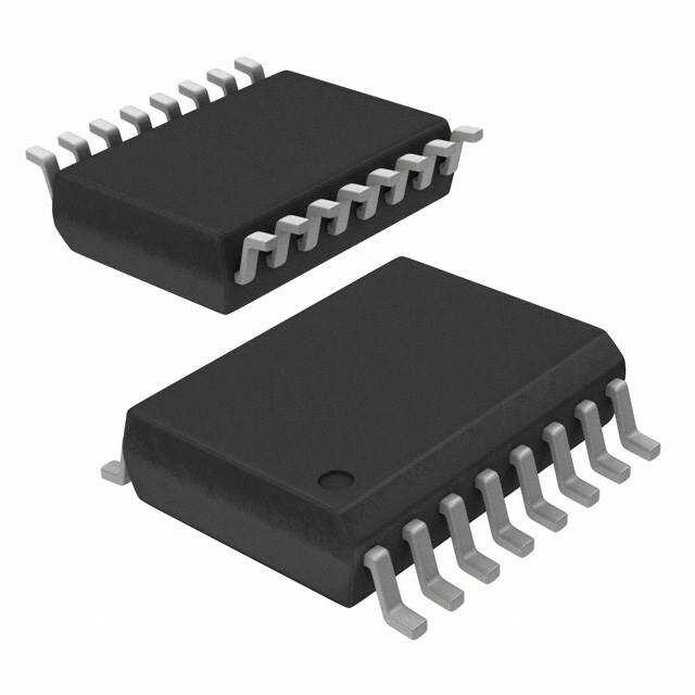
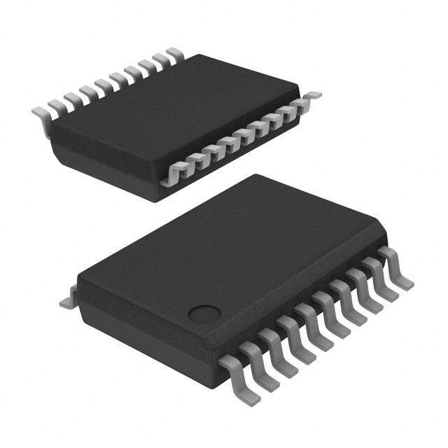
| 描述 | IC LINE RCVR QUAD CMOS 16-SOIC总线接收器 3V Enhancd CMOS Quad Diff Line Receiver |
| 产品分类 | |
| 品牌 | Texas Instruments |
| 产品手册 | |
| 产品图片 |
|
| rohs | 否含铅 / 不符合限制有害物质指令(RoHS)规范要求 |
| 产品系列 | 逻辑集成电路,总线接收器,Texas Instruments DS26LV32ATM- |
| 数据手册 | |
| 产品型号 | DS26LV32ATM |
| 产品种类 | 总线接收器 |
| 供应商器件封装 | 16-SOIC N |
| 包装 | 管件 |
| 协议 | RS422 |
| 双工 | - |
| 商标 | Texas Instruments |
| 安装类型 | 表面贴装 |
| 安装风格 | SMD/SMT |
| 封装 | Tube |
| 封装/外壳 | 16-SOIC(0.154",3.90mm 宽) |
| 封装/箱体 | SOIC-16 Narrow |
| 工作温度 | -40°C ~ 85°C |
| 工作电源电压 | 3.3 V |
| 工厂包装数量 | 48 |
| 接口类型 | EIA/TIA-422-B, RS-422, V.11 |
| 接收器滞后 | 35mV |
| 接收机信号类型 | Differential |
| 接收机数量 | 4 |
| 数据速率 | - |
| 最大工作温度 | + 85 C |
| 最小工作温度 | - 40 C |
| 标准包装 | 48 |
| 电压-电源 | 3 V ~ 3.6 V |
| 电源电流 | 15 mA |
| 类型 | 接收器 |
| 系列 | DS26LV32AT |
| 驱动器/接收器数 | 0/4 |


- 商务部:美国ITC正式对集成电路等产品启动337调查
- 曝三星4nm工艺存在良率问题 高通将骁龙8 Gen1或转产台积电
- 太阳诱电将投资9.5亿元在常州建新厂生产MLCC 预计2023年完工
- 英特尔发布欧洲新工厂建设计划 深化IDM 2.0 战略
- 台积电先进制程称霸业界 有大客户加持明年业绩稳了
- 达到5530亿美元!SIA预计今年全球半导体销售额将创下新高
- 英特尔拟将自动驾驶子公司Mobileye上市 估值或超500亿美元
- 三星加码芯片和SET,合并消费电子和移动部门,撤换高东真等 CEO
- 三星电子宣布重大人事变动 还合并消费电子和移动部门
- 海关总署:前11个月进口集成电路产品价值2.52万亿元 增长14.8%


PDF Datasheet 数据手册内容提取
DS26LV32AT www.ti.com SNLS128C–APRIL1999–REVISEDFEBRUARY2013 DS26LV32AT 3V Enhanced CMOS Quad Differential Line Receiver CheckforSamples:DS26LV32AT FEATURES • AvailableinSOICandCLGAPackaging 1 • LowPowerCMOSDesign(30mWtypical) • StandardMicrocircuitDrawing(SMD)5962- 2 98585 • InteroperablewithExisting5VRS-422 Networks DESCRIPTION • IndustrialandMilitaryTemperatureRange The DS26LV32A is a high speed quad differential • ConformstoTIA/EIA-422-B(RS-422)andITU-T CMOS receiver that meets the requirements of both V.11Recommendation TIA/EIA-422-B and ITU-T V.11. The CMOS • 3.3VOperation DS26LV32AT features typical low static I of 9 mA CC which makes it ideal for battery powered and power • ±7VCommonModeRange@V =3V ID conscious applications. The TRI-STATE enables, EN • ±10VCommonModeRange@V =0.2V ID and EN*, allow the device to be active High or active • ReceiverOPENInputFailsafeFeature Low.Theenablesarecommontoallfourreceivers. • GuaranteedACParameter: The receiver output (RO) is guaranteed to be High – MaximumReceiverSkew: 4ns when the inputs are left open. The receiver can detect signals as low as ±200 mV over the common – MaximumTransitionTime: 10ns mode range of ±10V. The receiver outputs (RO) are • PinCompatiblewithDS26C32AT compatiblewithTTLandLVCMOSlevels. • 32MHzToggleFrequency • >6.5kESDTolerance(HBM) Connection Diagram TopView Figure1. SOICPackage SeePackageNumbersD0016AorNAD0016A 1 Pleasebeawarethatanimportantnoticeconcerningavailability,standardwarranty,anduseincriticalapplicationsof TexasInstrumentssemiconductorproductsanddisclaimerstheretoappearsattheendofthisdatasheet. Alltrademarksarethepropertyoftheirrespectiveowners. 2 PRODUCTIONDATAinformationiscurrentasofpublicationdate. Copyright©1999–2013,TexasInstrumentsIncorporated Products conform to specifications per the terms of the Texas Instruments standard warranty. Production processing does not necessarilyincludetestingofallparameters.
DS26LV32AT SNLS128C–APRIL1999–REVISEDFEBRUARY2013 www.ti.com Truth Table(1) Enables Inputs Output EN EN* RI+–RI− RO L H X Z Allother V ≥+0.2V H ID combinationsof V ≤−0.2V L enableinputs ID Open(2) H (1) L=LogicLow H=LogicHigh X=Irrelevant Z=TRI-STATE (2) Open,notterminated Thesedeviceshavelimitedbuilt-inESDprotection.Theleadsshouldbeshortedtogetherorthedeviceplacedinconductivefoam duringstorageorhandlingtopreventelectrostaticdamagetotheMOSgates. Absolute Maximum Ratings(1)(2) SupplyVoltage(V ) −0.5Vto+7V CC EnableInputVoltage(EN,EN*) −0.5VtoV +0.5V CC ReceiverInputVoltage(V :RI+,RI−) ±14V ID ReceiverInputVoltage (VCM:RI+,RI−) ±14V ReceiverOutputVoltage(RO) −0.5VtoV +0.5V CC ReceiverOutputCurrent(RO) ±25mAMaximum MaximumPackagePowerDissipation@+25°C D0016APackage 1190mW NAD0016APackage 1087mW DerateD0016APackage9.8mW/°Cabove+25°C DerateNAD0016APackage7.3mW/°Cabove+25°C StorageTemperatureRange −65°Cto+150°C LeadTemperatureRangeSoldering (4Sec.) +260°C ESDRatings(HBM,1.5kΩ,100pF) ReceiverInputsandEnables ≥6.5kV OtherPins ≥2kV (1) “AbsoluteMaximumratings”arethosevaluesbeyondwhichthesafetyofthedevicecannotbeguaranteed.Theyarenotmeanttoimply thatthedevicesshouldbeoperatedattheselimits.TheElectricalCharacteristicsspecifiesconditionsofdeviceoperation. (2) IfMilitary/Aerospacespecifieddevicesarerequired,pleasecontacttheTISalesOffice/Distributorsforavailabilityandspecifications. Recommended Operating Conditions Min Typ Max Units SupplyVoltage(V ) 3.0 3.3 3.6 V CC OperatingFreeAirTemperatureRange(T ) A DS26LV32AT −40 +25 +85 °C DS26LV32AW −55 +25 +125 °C 2 SubmitDocumentationFeedback Copyright©1999–2013,TexasInstrumentsIncorporated ProductFolderLinks:DS26LV32AT
DS26LV32AT www.ti.com SNLS128C–APRIL1999–REVISEDFEBRUARY2013 Electrical Characteristics (1) (2) OverSupplyVoltageandOperatingTemperatureranges,unlessotherwisespecified. Parameter TestConditions Pin Min Typ Max Units V DifferentialInputThreshold V =V orV V =−7Vto+7V, −200 ±17.5 +200 mV TH OUT OH OL CM T =-40°Cto A +85°C RI+, V =−0.5Vto -200 +200 mV CM RI− +5.5V,T =-55°C A to+125°C(3) V Hysteresis V =1.5V 35 mV HY CM V MinimumHighLevelInput IH 2.0 V Voltage EN, V MaximumLowLevelInput EN* IL 0.8 V Voltage R InputResistance V =−7V,+7V,T =-40°Cto+85°C IN IN A 5.0 8.5 kΩ (OtherInput=GND) V =−0.5V,+5.5V,T =-55°Cto+125°C 5.0 kΩ IN A (OtherInput=GND) (3) I InputCurrent V =+10V T =-40°Cto 0 1.1 1.8 mA IN IN A +85°C (OtherInput=0V, V =+3V RI+, 0 0.27 mA IN RI− PowerOn,or V =0.5V −0.02 mA IN V =0V) V =−3V 0 −0.43 mA CC IN V =−10V 0 −1.26 −2.2 mA IN V =−0.5V T =-55°Cto 0 -1.8 mA IN A +125°C (3) V =5.5V 0 1.8 mA IN I InputCurrent V =0VtoV EN, ±1 μA EN IN CC EN* V HighLevelOutputVoltage I =−6mA,V =+1V OH OH ID 2.4 3 V I =−6mA,V =OPEN OH ID V HighLevelOutputVoltage I =−100μA,V =+1V OH OH ID V −0.1 V CC I =−100μA,V =OPEN OH ID RO V LowLevelOutputVoltage I =+6mA,V =−1V 0.13 0.5 V OL OL ID I OutputTRI-STATELeakage V =V orGND OZ OUT CC Current ±50 μA EN=V ,EN*=V IL IH I OutputShortCircuitCurrent V =0V,V ≥|200mV| (4) −10 −35 −70 mA SC O ID I PowerSupplyCurrent NoLoad,AllRI+, T =-40°Cto V 9 15 mA CC A CC R1−=OPEN,EN, +85°C EN*=V orGND CC T =-55°Cto 20 mA A +125°C (1) Currentintodevicepinsisdefinedaspositive.Currentoutofdevicepinsisdefinedasnegative.Allvoltagesarereferencedtoground exceptV . ID (2) Alltypicalsaregivenfor:V =+3.3V,T =+25°C. CC A (3) ThisparameterdoesnotmeettheTIA/EIA-422-Bspecification. (4) Shortoneoutputatatimetoground.Donotexceedpackage. Copyright©1999–2013,TexasInstrumentsIncorporated SubmitDocumentationFeedback 3 ProductFolderLinks:DS26LV32AT
DS26LV32AT SNLS128C–APRIL1999–REVISEDFEBRUARY2013 www.ti.com Switching Characteristics - Industrial (1) (2) OverSupplyVoltageand-40°Cto+85°COperatingTemperaturerange,unlessotherwisespecified. Parameter TestConditions Min Typ Max Units t PropagationDelayHightoLow C =15pF,V =1.5V(Figure2andFigure3) 6 17.5 35 ns PHL L CM t PropagationDelayLowtoHigh 6 17.8 35 ns PLH t RiseTime(20%to80%) 4.1 10 ns r t FallTime(80%to20%) 3.3 10 ns f t DisableTime C =50pF,V =1.5V(Figure4andFigure5) 40 ns PHZ L CM t DisableTime 40 ns PLZ t EnableTime 40 ns PZH t EnableTime 40 ns PZL t Skew,|t −t | (3) C =15pF,V =1.5V 0.3 4 ns SK1 PHL PLH L CM t Skew,PintoPin (4) 0.6 4 ns SK2 t Skew,ParttoPart (2) 7 17 ns SK3 f MaximumOperatingFrequency C =15pF,V =1.5V 32 MHz MAX L CM (5) (1) Alltypicalsaregivenfor:V =+3.3V,T =+25°C. CC A (2) t isthedifferenceinpropagationdelaytimesbetweenanychannelsofanydevices.Thisspecification(maximumlimit)appliesto SK3 deviceswithinV ±0.1Vofoneanother,andaDeltaT =±5°C(betweendevices)withintheoperatingtemperaturerange.This CC A parameterisguaranteedbydesignandcharacterization. (3) t isthe|t –t |ofachannel. SK1 PHL PLH (4) t isthemaximumskewbetweenanytwochannelswithinadevice,eitheredge. SK2 (5) Allchannelsswitching,OutputDutyCyclecriteriais40%/60%measuredat50%.Input=1Vto2V,50%DutyCycle,t/t ≤5ns.This r f parameterisguaranteedbydesignandcharacterization. Switching Characteristics - Military OverSupplyVoltageand-55°Cto+125°COperatingTemperaturerange,unlessotherwisespecified. Parameter TestConditions Min Max Units t PropagationDelayHightoLow C =50pF,V =1.5V(Figure2andFigure3) 6 45 ns PHL L CM t PropagationDelayLowtoHigh 6 45 ns PLH t DisableTime C =50pF,V =1.5V(Figure4andFigure5) 50 ns PHZ L CM t DisableTime 50 ns PLZ t EnableTime 50 ns PZH t EnableTime 50 ns PZL t Skew,|t −t | (1) C =50pF,V =1.5V 6 ns SK1 PHL PLH L CM t Skew,PintoPin (2) 6 ns SK2 (1) t isthe|t –t |ofachannel. SK1 PHL PLH (2) t isthemaximumskewbetweenanytwochannelswithinadevice,eitheredge. SK2 4 SubmitDocumentationFeedback Copyright©1999–2013,TexasInstrumentsIncorporated ProductFolderLinks:DS26LV32AT
DS26LV32AT www.ti.com SNLS128C–APRIL1999–REVISEDFEBRUARY2013 PARAMETER MEASUREMENT INFORMATION A. Generatorwaveformforalltestsunlessotherwisespecified:f=1MHz,DutyCycle=50%,Z =50Ω,t ≤10ns,t ≤ O r f 10ns. B. C includesprobeandjigcapacitance. L Figure2. ReceiverPropagationDelayandTransitionTimeTestCircuit A. Generatorwaveformforalltestsunlessotherwisespecified:f=1MHz,DutyCycle=50%,Z =50Ω,t ≤10ns,t ≤ O r f 10ns. B. C includesprobeandjigcapacitance. L C. Formilitarygradeproduct,t ≤6nsandt ≤6ns. r f D. Formilitarygradeproductthemeasurepointis1/2V fort ,t ,t ,andt . CC PLH PHL PZL PZH Figure3. ReceiverPropagationDelayandTransitionTimeWaveform Figure4. ReceiverTRI-STATETestCircuit Copyright©1999–2013,TexasInstrumentsIncorporated SubmitDocumentationFeedback 5 ProductFolderLinks:DS26LV32AT
DS26LV32AT SNLS128C–APRIL1999–REVISEDFEBRUARY2013 www.ti.com A. Generatorwaveformforalltestsunlessotherwisespecified:f=1MHz,DutyCycle=50%,Z =50Ω,t ≤10ns,t ≤ O r f 10ns. B. C includesprobeandjigcapacitance. L C. Formilitarygradeproduct,t ≤6nsandt ≤6ns. r f D. Formilitarygradeproductthemeasurepointis1/2V fort ,t ,t ,andt . CC PLH PHL PZL PZH Figure5. ReceiverTRI-STATEOutputEnableandDisableWaveforms 6 SubmitDocumentationFeedback Copyright©1999–2013,TexasInstrumentsIncorporated ProductFolderLinks:DS26LV32AT
DS26LV32AT www.ti.com SNLS128C–APRIL1999–REVISEDFEBRUARY2013 TYPICAL APPLICATION INFORMATION General application guidelines and hints for differential drivers and receivers may be found in the following applicationnotes: • AN-214 • AN-457 • AN-805 • AN-847 • AN-903 • AN-912 • AN-916 PowerDecouplingRecommendations: Bypass caps must be used on power pins. High frequency ceramic (surface mount is recommended) 0.1 μF in parallel with 0.01 μF at the power supply pin. A 10 μF or greater solid tantalum or electrolytic should be connectedatthepowerentrypointontheprintedcircuitboard. R isoptionalalthoughhighlyrecommendedtoreducereflection T Figure6. TypicalReceiverConnections Figure7. TypicalReceiverOutputWaveforms Copyright©1999–2013,TexasInstrumentsIncorporated SubmitDocumentationFeedback 7 ProductFolderLinks:DS26LV32AT
DS26LV32AT SNLS128C–APRIL1999–REVISEDFEBRUARY2013 www.ti.com Figure8. TypicalReceiverInputCircuit Figure9. TypicalI vsFrequency CC Figure10. ReceiverI vsV (PowerOnorPowerOff) IN IN 8 SubmitDocumentationFeedback Copyright©1999–2013,TexasInstrumentsIncorporated ProductFolderLinks:DS26LV32AT
DS26LV32AT www.ti.com SNLS128C–APRIL1999–REVISEDFEBRUARY2013 Figure11. I vsV OL OL Figure12. I vsV OH OH Copyright©1999–2013,TexasInstrumentsIncorporated SubmitDocumentationFeedback 9 ProductFolderLinks:DS26LV32AT
DS26LV32AT SNLS128C–APRIL1999–REVISEDFEBRUARY2013 www.ti.com REVISION HISTORY ChangesfromRevisionB(February2013)toRevisionC Page • ChangedlayoutofNationalDataSheettoTIformat............................................................................................................ 9 10 SubmitDocumentationFeedback Copyright©1999–2013,TexasInstrumentsIncorporated ProductFolderLinks:DS26LV32AT
PACKAGE OPTION ADDENDUM www.ti.com 23-Aug-2017 PACKAGING INFORMATION Orderable Device Status Package Type Package Pins Package Eco Plan Lead/Ball Finish MSL Peak Temp Op Temp (°C) Device Marking Samples (1) Drawing Qty (2) (6) (3) (4/5) DS26LV32ATM LIFEBUY SOIC D 16 48 TBD Call TI Call TI -40 to 85 DS26LV32A TM DS26LV32ATM/NOPB ACTIVE SOIC D 16 48 Green (RoHS CU SN Level-1-260C-UNLIM -40 to 85 DS26LV32A & no Sb/Br) TM DS26LV32ATMX LIFEBUY SOIC D 16 2500 TBD Call TI Call TI -40 to 85 DS26LV32A TM DS26LV32ATMX/NOPB ACTIVE SOIC D 16 2500 Green (RoHS CU SN Level-1-260C-UNLIM -40 to 85 DS26LV32A & no Sb/Br) TM (1) The marketing status values are defined as follows: ACTIVE: Product device recommended for new designs. LIFEBUY: TI has announced that the device will be discontinued, and a lifetime-buy period is in effect. NRND: Not recommended for new designs. Device is in production to support existing customers, but TI does not recommend using this part in a new design. PREVIEW: Device has been announced but is not in production. Samples may or may not be available. OBSOLETE: TI has discontinued the production of the device. (2) RoHS: TI defines "RoHS" to mean semiconductor products that are compliant with the current EU RoHS requirements for all 10 RoHS substances, including the requirement that RoHS substance do not exceed 0.1% by weight in homogeneous materials. Where designed to be soldered at high temperatures, "RoHS" products are suitable for use in specified lead-free processes. TI may reference these types of products as "Pb-Free". RoHS Exempt: TI defines "RoHS Exempt" to mean products that contain lead but are compliant with EU RoHS pursuant to a specific EU RoHS exemption. Green: TI defines "Green" to mean the content of Chlorine (Cl) and Bromine (Br) based flame retardants meet JS709B low halogen requirements of <=1000ppm threshold. Antimony trioxide based flame retardants must also meet the <=1000ppm threshold requirement. (3) MSL, Peak Temp. - The Moisture Sensitivity Level rating according to the JEDEC industry standard classifications, and peak solder temperature. (4) There may be additional marking, which relates to the logo, the lot trace code information, or the environmental category on the device. (5) Multiple Device Markings will be inside parentheses. Only one Device Marking contained in parentheses and separated by a "~" will appear on a device. If a line is indented then it is a continuation of the previous line and the two combined represent the entire Device Marking for that device. (6) Lead/Ball Finish - Orderable Devices may have multiple material finish options. Finish options are separated by a vertical ruled line. Lead/Ball Finish values may wrap to two lines if the finish value exceeds the maximum column width. Important Information and Disclaimer:The information provided on this page represents TI's knowledge and belief as of the date that it is provided. TI bases its knowledge and belief on information provided by third parties, and makes no representation or warranty as to the accuracy of such information. Efforts are underway to better integrate information from third parties. TI has taken and Addendum-Page 1
PACKAGE OPTION ADDENDUM www.ti.com 23-Aug-2017 continues to take reasonable steps to provide representative and accurate information but may not have conducted destructive testing or chemical analysis on incoming materials and chemicals. TI and TI suppliers consider certain information to be proprietary, and thus CAS numbers and other limited information may not be available for release. In no event shall TI's liability arising out of such information exceed the total purchase price of the TI part(s) at issue in this document sold by TI to Customer on an annual basis. Addendum-Page 2
PACKAGE MATERIALS INFORMATION www.ti.com 10-Aug-2018 TAPE AND REEL INFORMATION *Alldimensionsarenominal Device Package Package Pins SPQ Reel Reel A0 B0 K0 P1 W Pin1 Type Drawing Diameter Width (mm) (mm) (mm) (mm) (mm) Quadrant (mm) W1(mm) DS26LV32ATMX/NOPB SOIC D 16 2500 330.0 16.4 6.5 10.3 2.3 8.0 16.0 Q1 PackMaterials-Page1
PACKAGE MATERIALS INFORMATION www.ti.com 10-Aug-2018 *Alldimensionsarenominal Device PackageType PackageDrawing Pins SPQ Length(mm) Width(mm) Height(mm) DS26LV32ATMX/NOPB SOIC D 16 2500 367.0 367.0 35.0 PackMaterials-Page2
None
IMPORTANTNOTICE TexasInstrumentsIncorporated(TI)reservestherighttomakecorrections,enhancements,improvementsandotherchangestoits semiconductorproductsandservicesperJESD46,latestissue,andtodiscontinueanyproductorserviceperJESD48,latestissue.Buyers shouldobtainthelatestrelevantinformationbeforeplacingordersandshouldverifythatsuchinformationiscurrentandcomplete. TI’spublishedtermsofsaleforsemiconductorproducts(http://www.ti.com/sc/docs/stdterms.htm)applytothesaleofpackagedintegrated circuitproductsthatTIhasqualifiedandreleasedtomarket.AdditionaltermsmayapplytotheuseorsaleofothertypesofTIproductsand services. ReproductionofsignificantportionsofTIinformationinTIdatasheetsispermissibleonlyifreproductioniswithoutalterationandis accompaniedbyallassociatedwarranties,conditions,limitations,andnotices.TIisnotresponsibleorliableforsuchreproduced documentation.Informationofthirdpartiesmaybesubjecttoadditionalrestrictions.ResaleofTIproductsorserviceswithstatements differentfromorbeyondtheparametersstatedbyTIforthatproductorservicevoidsallexpressandanyimpliedwarrantiesforthe associatedTIproductorserviceandisanunfairanddeceptivebusinesspractice.TIisnotresponsibleorliableforanysuchstatements. BuyersandotherswhoaredevelopingsystemsthatincorporateTIproducts(collectively,“Designers”)understandandagreethatDesigners remainresponsibleforusingtheirindependentanalysis,evaluationandjudgmentindesigningtheirapplicationsandthatDesignershave fullandexclusiveresponsibilitytoassurethesafetyofDesigners'applicationsandcomplianceoftheirapplications(andofallTIproducts usedinorforDesigners’applications)withallapplicableregulations,lawsandotherapplicablerequirements.Designerrepresentsthat,with respecttotheirapplications,Designerhasallthenecessaryexpertisetocreateandimplementsafeguardsthat(1)anticipatedangerous consequencesoffailures,(2)monitorfailuresandtheirconsequences,and(3)lessenthelikelihoodoffailuresthatmightcauseharmand takeappropriateactions.DesigneragreesthatpriortousingordistributinganyapplicationsthatincludeTIproducts,Designerwill thoroughlytestsuchapplicationsandthefunctionalityofsuchTIproductsasusedinsuchapplications. TI’sprovisionoftechnical,applicationorotherdesignadvice,qualitycharacterization,reliabilitydataorotherservicesorinformation, including,butnotlimitedto,referencedesignsandmaterialsrelatingtoevaluationmodules,(collectively,“TIResources”)areintendedto assistdesignerswhoaredevelopingapplicationsthatincorporateTIproducts;bydownloading,accessingorusingTIResourcesinany way,Designer(individuallyor,ifDesignerisactingonbehalfofacompany,Designer’scompany)agreestouseanyparticularTIResource solelyforthispurposeandsubjecttothetermsofthisNotice. TI’sprovisionofTIResourcesdoesnotexpandorotherwisealterTI’sapplicablepublishedwarrantiesorwarrantydisclaimersforTI products,andnoadditionalobligationsorliabilitiesarisefromTIprovidingsuchTIResources.TIreservestherighttomakecorrections, enhancements,improvementsandotherchangestoitsTIResources.TIhasnotconductedanytestingotherthanthatspecifically describedinthepublisheddocumentationforaparticularTIResource. Designerisauthorizedtouse,copyandmodifyanyindividualTIResourceonlyinconnectionwiththedevelopmentofapplicationsthat includetheTIproduct(s)identifiedinsuchTIResource.NOOTHERLICENSE,EXPRESSORIMPLIED,BYESTOPPELOROTHERWISE TOANYOTHERTIINTELLECTUALPROPERTYRIGHT,ANDNOLICENSETOANYTECHNOLOGYORINTELLECTUALPROPERTY RIGHTOFTIORANYTHIRDPARTYISGRANTEDHEREIN,includingbutnotlimitedtoanypatentright,copyright,maskworkright,or otherintellectualpropertyrightrelatingtoanycombination,machine,orprocessinwhichTIproductsorservicesareused.Information regardingorreferencingthird-partyproductsorservicesdoesnotconstitutealicensetousesuchproductsorservices,orawarrantyor endorsementthereof.UseofTIResourcesmayrequirealicensefromathirdpartyunderthepatentsorotherintellectualpropertyofthe thirdparty,oralicensefromTIunderthepatentsorotherintellectualpropertyofTI. TIRESOURCESAREPROVIDED“ASIS”ANDWITHALLFAULTS.TIDISCLAIMSALLOTHERWARRANTIESOR REPRESENTATIONS,EXPRESSORIMPLIED,REGARDINGRESOURCESORUSETHEREOF,INCLUDINGBUTNOTLIMITEDTO ACCURACYORCOMPLETENESS,TITLE,ANYEPIDEMICFAILUREWARRANTYANDANYIMPLIEDWARRANTIESOF MERCHANTABILITY,FITNESSFORAPARTICULARPURPOSE,ANDNON-INFRINGEMENTOFANYTHIRDPARTYINTELLECTUAL PROPERTYRIGHTS.TISHALLNOTBELIABLEFORANDSHALLNOTDEFENDORINDEMNIFYDESIGNERAGAINSTANYCLAIM, INCLUDINGBUTNOTLIMITEDTOANYINFRINGEMENTCLAIMTHATRELATESTOORISBASEDONANYCOMBINATIONOF PRODUCTSEVENIFDESCRIBEDINTIRESOURCESOROTHERWISE.INNOEVENTSHALLTIBELIABLEFORANYACTUAL, DIRECT,SPECIAL,COLLATERAL,INDIRECT,PUNITIVE,INCIDENTAL,CONSEQUENTIALOREXEMPLARYDAMAGESIN CONNECTIONWITHORARISINGOUTOFTIRESOURCESORUSETHEREOF,ANDREGARDLESSOFWHETHERTIHASBEEN ADVISEDOFTHEPOSSIBILITYOFSUCHDAMAGES. UnlessTIhasexplicitlydesignatedanindividualproductasmeetingtherequirementsofaparticularindustrystandard(e.g.,ISO/TS16949 andISO26262),TIisnotresponsibleforanyfailuretomeetsuchindustrystandardrequirements. WhereTIspecificallypromotesproductsasfacilitatingfunctionalsafetyorascompliantwithindustryfunctionalsafetystandards,such productsareintendedtohelpenablecustomerstodesignandcreatetheirownapplicationsthatmeetapplicablefunctionalsafetystandards andrequirements.Usingproductsinanapplicationdoesnotbyitselfestablishanysafetyfeaturesintheapplication.Designersmust ensurecompliancewithsafety-relatedrequirementsandstandardsapplicabletotheirapplications.DesignermaynotuseanyTIproductsin life-criticalmedicalequipmentunlessauthorizedofficersofthepartieshaveexecutedaspecialcontractspecificallygoverningsuchuse. Life-criticalmedicalequipmentismedicalequipmentwherefailureofsuchequipmentwouldcauseseriousbodilyinjuryordeath(e.g.,life support,pacemakers,defibrillators,heartpumps,neurostimulators,andimplantables).Suchequipmentincludes,withoutlimitation,all medicaldevicesidentifiedbytheU.S.FoodandDrugAdministrationasClassIIIdevicesandequivalentclassificationsoutsidetheU.S. TImayexpresslydesignatecertainproductsascompletingaparticularqualification(e.g.,Q100,MilitaryGrade,orEnhancedProduct). Designersagreethatithasthenecessaryexpertisetoselecttheproductwiththeappropriatequalificationdesignationfortheirapplications andthatproperproductselectionisatDesigners’ownrisk.Designersaresolelyresponsibleforcompliancewithalllegalandregulatory requirementsinconnectionwithsuchselection. DesignerwillfullyindemnifyTIanditsrepresentativesagainstanydamages,costs,losses,and/orliabilitiesarisingoutofDesigner’snon- compliancewiththetermsandprovisionsofthisNotice. MailingAddress:TexasInstruments,PostOfficeBox655303,Dallas,Texas75265 Copyright©2018,TexasInstrumentsIncorporated