ICGOO在线商城 > 传感器,变送器 > 运动传感器 - 加速计 > ADXL345TCCZ-EP
 Datasheet下载
- 型号: ADXL345TCCZ-EP
- 制造商: Analog
- 库位|库存: xxxx|xxxx
- 要求:
| 数量阶梯 | 香港交货 | 国内含税 |
| +xxxx | $xxxx | ¥xxxx |
查看当月历史价格
查看今年历史价格
ADXL345TCCZ-EP产品简介:
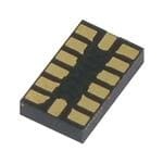
ICGOO电子元器件商城为您提供ADXL345TCCZ-EP由Analog设计生产,在icgoo商城现货销售,并且可以通过原厂、代理商等渠道进行代购。 ADXL345TCCZ-EP价格参考。AnalogADXL345TCCZ-EP封装/规格:运动传感器 - 加速计, Accelerometer X, Y, Z Axis ±2g, 4g, 8g, 16g 0.05Hz ~ 1.6kHz 14-LGA (3x5)。您可以下载ADXL345TCCZ-EP参考资料、Datasheet数据手册功能说明书,资料中有ADXL345TCCZ-EP 详细功能的应用电路图电压和使用方法及教程。
ADXL345TCCZ-EP是由Analog Devices Inc.(亚德诺半导体公司)生产的运动传感器,具体为一款三轴加速度计。这款器件具有广泛的应用场景,尤其适用于对精度、功耗和尺寸有较高要求的工业及消费类电子产品中。

1. 消费电子设备:在智能手机、平板电脑等移动设备中,ADXL345TCCZ-EP可以用来检测设备的姿态变化,实现屏幕自动旋转、游戏控制等功能;同时也可以用于计步器、健身追踪器等可穿戴设备中,监测用户的运动状态,如跑步、行走等,并记录相关数据。

2. 无人机与机器人技术:作为惯性测量单元(IMU)的一部分,它能够提供精确的倾斜角信息,帮助无人机保持稳定飞行姿态或让机器人更好地感知周围环境并调整自身位置。此外,在自动驾驶汽车领域,该传感器可用于辅助导航系统,确保车辆行驶平稳安全。

3. 工业自动化:可用于振动监测,通过对机械设备运行时产生的微小震动进行实时监控,提前预警可能出现的问题,从而减少故障发生率并延长设备使用寿命。另外,在物流运输过程中,它还可以被安装于包装箱内,以跟踪货物的状态,防止因不当搬运造成的损坏。

4. 医疗健康领域:在一些医疗仪器中,例如心电图机、呼吸机等,此款加速度计可以帮助监测患者的身体活动情况或者呼吸频率等生理参数,为医生诊断病情提供参考依据。

总之,ADXL345TCCZ-EP凭借其高灵敏度、低功耗以及紧凑的设计,在众多需要精确测量加速度变化的应用场合都表现出色。
| 参数 | 数值 |
| 产品目录 | |
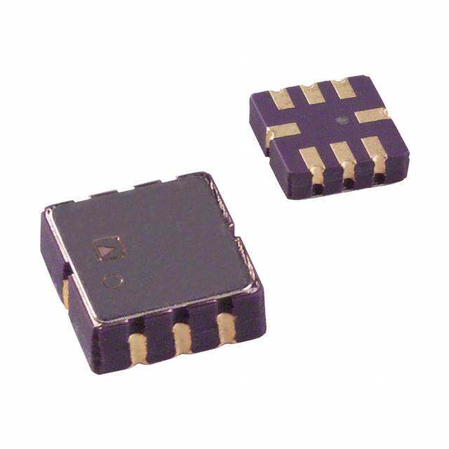
| 描述 | ACCELEROMETER DGTL 3AXIS 14LGA |
| 产品分类 | 加速计 |
| 品牌 | Analog Devices Inc |
| 数据手册 | |
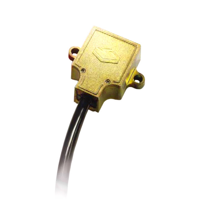
| 产品图片 |
|
| 产品型号 | ADXL345TCCZ-EP |
| PCN组件/产地 | |
| PCN设计/规格 | |
| rohs | 无铅 / 不受限制有害物质指令(RoHS)规范要求限制 |
| 产品系列 | iMEMS® |
| 供应商器件封装 | 14-LGA(3x5) |
| 其它名称 | ADXL345TCCZEP |
| 加速度范围 | ±2g, 4g, 8g, 16g |
| 安装类型 | 表面贴装 |
| 封装/外壳 | 14-VFLGA |
| 带宽 | 6.25Hz ~ 3.2kHz 可选 |
| 接口 | 串行 |
| 标准包装 | 1 |
| 灵敏度 | 256LSB/g,128LSB/g,64LSB/g,32LSB/g |
| 电压-电源 | 2 V ~ 3.6 V |
| 视频文件 | http://www.digikey.cn/classic/video.aspx?PlayerID=1364138032001&width=640&height=505&videoID=2245193160001http://www.digikey.cn/classic/video.aspx?PlayerID=1364138032001&width=640&height=505&videoID=2245193171001http://www.digikey.cn/classic/video.aspx?PlayerID=1364138032001&width=640&height=505&videoID=2245193161001http://www.digikey.cn/classic/video.aspx?PlayerID=1364138032001&width=640&height=505&videoID=2245193172001 |
| 轴 | X,Y,Z |
| 输出类型 | I²C, SPI |


- 商务部:美国ITC正式对集成电路等产品启动337调查
- 曝三星4nm工艺存在良率问题 高通将骁龙8 Gen1或转产台积电
- 太阳诱电将投资9.5亿元在常州建新厂生产MLCC 预计2023年完工
- 英特尔发布欧洲新工厂建设计划 深化IDM 2.0 战略
- 台积电先进制程称霸业界 有大客户加持明年业绩稳了
- 达到5530亿美元!SIA预计今年全球半导体销售额将创下新高
- 英特尔拟将自动驾驶子公司Mobileye上市 估值或超500亿美元
- 三星加码芯片和SET,合并消费电子和移动部门,撤换高东真等 CEO
- 三星电子宣布重大人事变动 还合并消费电子和移动部门
- 海关总署:前11个月进口集成电路产品价值2.52万亿元 增长14.8%

PDF Datasheet 数据手册内容提取
3-Axis, ±2 g/±4 g/±8 g/±16 g Digital Accelerometer Data Sheet ADXL345 FEATURES GENERAL DESCRIPTION Ultralow power: as low as 23 µA in measurement mode and The ADXL345 is a small, thin, ultralow power, 3-axis accelerometer 0.1 µA in standby mode at VS = 2.5 V (typical) with high resolution (13-bit) measurement at up to ±16 g. Digital Power consumption scales automatically with bandwidth output data is formatted as 16-bit twos complement and is acces- User-selectable resolution sible through either a SPI (3- or 4-wire) or I2C digital interface. Fixed 10-bit resolution The ADXL345 is well suited for mobile device applications. It Full resolution, where resolution increases with g range, measures the static acceleration of gravity in tilt-sensing appli- up to 13-bit resolution at ±16 g (maintaining 4 mg/LSB cations, as well as dynamic acceleration resulting from motion scale factor in all g ranges) or shock. Its high resolution (3.9 mg/LSB) enables measurement Embedded memory management system with FIFO of inclination changes less than 1.0°. technology minimizes host processor load Single tap/double tap detection Several special sensing functions are provided. Activity and Activity/inactivity monitoring inactivity sensing detect the presence or lack of motion by Free-fall detection comparing the acceleration on any axis with user-set thresholds. Supply voltage range: 2.0 V to 3.6 V Tap sensing detects single and double taps in any direction. Free- I/O voltage range: 1.7 V to V fall sensing detects if the device is falling. These functions can S SPI (3- and 4-wire) and I2C digital interfaces be mapped individually to either of two interrupt output pins. Flexible interrupt modes mappable to either interrupt pin An integrated memory management system with a 32-level first in, Measurement ranges selectable via serial command first out (FIFO) buffer can be used to store data to minimize host Bandwidth selectable via serial command processor activity and lower overall system power consumption. Wide temperature range (−40°C to +85°C) Low power modes enable intelligent motion-based power 10,000 g shock survival management with threshold sensing and active acceleration Pb free/RoHS compliant measurement at extremely low power dissipation. Small and thin: 3 mm × 5 mm × 1 mm LGA package The ADXL345 is supplied in a small, thin, 3 mm × 5 mm × 1 mm, APPLICATIONS 14-lead, plastic package. Handsets Medical instrumentation Gaming and pointing devices Industrial instrumentation Personal navigation devices Hard disk drive (HDD) protection FUNCTIONAL BLOCK DIAGRAM VS VDD I/O ADXL345 POWER MANAGEMENT CONTROL INT1 SENSE ADC AND ELECTRONICS DIGITAL INTERRUPT 3-AXIS FILTER LOGIC INT2 SENSOR SDA/SDI/SDIO 32 FLIEFVOEL SERIAL I/O SDO/ALT ADDRESS SCL/SCLK GND CS 07925-001 Figure 1. Rev. E Document Feedback Information furnished by Analog Devices is believed to be accurate and reliable. However, no responsibility is assumed by Analog Devices for its use, nor for any infringements of patents or other One Technology Way, P.O. Box 9106, Norwood, MA 02062-9106, U.S.A. rights of third parties that may result from its use. Specifications subject to change without notice. No license is granted by implication or otherwise under any patent or patent rights of Analog Devices. Tel: 781.329.4700 ©2009–2015 Analog Devices, Inc. All rights reserved. Trademarks and registered trademarks are the property of their respective owners. Technical Support www.analog.com
ADXL345 Data Sheet TABLE OF CONTENTS Self-Test ....................................................................................... 22 Features .............................................................................................. 1 Register Map ................................................................................... 23 Applications ....................................................................................... 1 Register Definitions ................................................................... 24 General Description ......................................................................... 1 Applications Information .............................................................. 28 Functional Block Diagram .............................................................. 1 Power Supply Decoupling ......................................................... 28 Revision History ............................................................................... 3 Mechanical Considerations for Mounting .............................. 28 Specifications ..................................................................................... 4 Tap Detection .............................................................................. 28 Absolute Maximum Ratings ............................................................ 6 Threshold .................................................................................... 29 Thermal Resistance ...................................................................... 6 Link Mode ................................................................................... 29 Package Information .................................................................... 6 Sleep Mode vs. Low Power Mode............................................. 30 ESD Caution .................................................................................. 6 Offset Calibration ....................................................................... 30 Pin Configuration and Function Descriptions ............................. 7 Using Self-Test ............................................................................ 31 Typical Performance Characteristics ............................................. 8 Data Formatting of Upper Data Rates ..................................... 32 Theory of Operation ...................................................................... 13 Noise Performance ..................................................................... 33 Power Sequencing ...................................................................... 13 Operation at Voltages Other Than 2.5 V ................................ 33 Power Savings ............................................................................. 14 Offset Performance at Lowest Data Rates ............................... 34 Serial Communications ................................................................. 15 Axes of Acceleration Sensitivity ............................................... 35 SPI ................................................................................................. 15 Layout and Design Recommendations ................................... 36 I2C ................................................................................................. 18 Outline Dimensions ....................................................................... 37 Interrupts ..................................................................................... 20 Ordering Guide .......................................................................... 37 FIFO ............................................................................................. 21 Rev. E | Page 2 of 40
Data Sheet ADXL345 REVISION HISTORY 6/15—Rev. D to Rev. E Changes to Figure 36 to Figure 38 ................................................ 15 Changes to Features Section and General Changes to Table 9 and Table 10 ................................................... 16 Description Section ........................................................................... 1 Changes to I2C Section and Table 11 ............................................ 17 Change to Figure 36 ........................................................................ 15 Changes to Table 12 ........................................................................ 18 Change to FIFO Section ................................................................. 21 Changes to Interrupts Section, Activity Section, Inactivity Section, and FREE_FALL Section ................................................. 19 2/13—Rev. C to Rev. D Added Table 13 ................................................................................ 19 Changes to Figure 13, Figure 14, and Figure 15 ............................ 9 Changes to FIFO Section ............................................................... 20 Change to Table 15 .......................................................................... 22 Changes to Self-Test Section and Table 15 to Table 18 .............. 21 Added Figures 42 and Table 14 ..................................................... 21 5/11—Rev. B to Rev. C Changes to Table 19 ........................................................................ 22 Added Preventing Bus Traffic Errors Section ............................ 15 Changes to Register 0x1D—THRESH_TAP (Read/Write) Changes to Figure 37, Figure 38, Figure 39 ................................. 16 Section, Register 0x1E, Register 0x1F, Register 0x20—OFSX, Changes to Table 12 ........................................................................ 19 OFSY, OSXZ (Read/Write) Section, Register 0x21—DUR Changes to Using Self-Test Section ............................................... 31 (Read/Write) Section, Register 0x22—Latent (Read/Write) Changes to Axes of Acceleration Sensitivity Section .................. 35 Section, and Register 0x23—Window (Read/Write) Section ... 23 Changes to ACT_X Enable Bits and INACT_X Enable Bit 11/10—Rev. A to Rev. B Section, Register 0x28—THRESH_FF (Read/Write) Section, Change to 0 g Offset vs. Temperature for Z-Axis Parameter, Register 0x29—TIME_FF (Read/Write) Section, Asleep Bit Table 1 ................................................................................................. 4 Section, and AUTO_SLEEP Bit Section ....................................... 24 Changes to Figure 10 to Figure 15 .................................................. 9 Changes to Sleep Bit Section ......................................................... 25 Changes to Ordering Guide ........................................................... 37 Changes to Power Supply Decoupling Section, Mechanical Considerations for Mounting Section, and Tap Detection 4/10—Rev. 0 to Rev. A Section .............................................................................................. 27 Changes to Features Section and General Changes to Threshold Section ....................................................... 28 Description Section ........................................................................... 1 Changes to Sleep Mode vs. Low Power Mode Section ............... 29 Changes to Specifications Section ................................................... 3 Added Offset Calibration Section ................................................. 29 Changes to Table 2 and Table 3 ....................................................... 5 Changes to Using Self-Test Section .............................................. 30 Added Package Information Section, Figure 2, and Table 4; Added Data Formatting of Upper Data Rates Section, Figure 48, Renumbered Sequentially ................................................................ 5 and Figure 49 ................................................................................... 31 Changes to Pin 12 Description, Table 5 ......................................... 6 Added Noise Performance Section, Figure 50 to Figure 52, and Added Typical Performance Characteristics Section ................... 7 Operation at Voltages Other Than 2.5 V Section ....................... 32 Changes to Theory of Operation Section and Power Sequencing Added Offset Performance at Lowest Data Rates Section and Section .............................................................................................. 12 Figure 53 to Figure 55 ..................................................................... 33 Changes to Powers Savings Section, Table 7, Table 8, Auto Sleep Mode Section, and Standby Mode Section .................................. 13 6/09—Revision 0: Initial Version Changes to SPI Section ................................................................... 14 Rev. E | Page 3 of 40
ADXL345 Data Sheet SPECIFICATIONS T = 25°C, V = 2.5 V, V = 1.8 V, acceleration = 0 g, C = 10 µF tantalum, C = 0.1 µF, output data rate (ODR) = 800 Hz, unless A S DD I/O S I/O otherwise noted. All minimum and maximum specifications are guaranteed. Typical specifications are not guaranteed. Table 1. Parameter Test Conditions Min Typ1 Max Unit SENSOR INPUT Each axis Measurement Range User selectable ±2, ±4, ±8, ±16 g Nonlinearity Percentage of full scale ±0.5 % Inter-Axis Alignment Error ±0.1 Degrees Cross-Axis Sensitivity2 ±1 % OUTPUT RESOLUTION Each axis All g Ranges 10-bit resolution 10 Bits ±2 g Range Full resolution 10 Bits ±4 g Range Full resolution 11 Bits ±8 g Range Full resolution 12 Bits ±16 g Range Full resolution 13 Bits SENSITIVITY Each axis Sensitivity at X , Y , Z All g-ranges, full resolution 230 256 282 LSB/g OUT OUT OUT ±2 g, 10-bit resolution 230 256 282 LSB/g ±4 g, 10-bit resolution 115 128 141 LSB/g ±8 g, 10-bit resolution 57 64 71 LSB/g ±16 g, 10-bit resolution 29 32 35 LSB/g Sensitivity Deviation from Ideal All g-ranges ±1.0 % Scale Factor at X , Y , Z All g-ranges, full resolution 3.5 3.9 4.3 mg/LSB OUT OUT OUT ±2 g, 10-bit resolution 3.5 3.9 4.3 mg/LSB ±4 g, 10-bit resolution 7.1 7.8 8.7 mg/LSB ±8 g, 10-bit resolution 14.1 15.6 17.5 mg/LSB ±16 g, 10-bit resolution 28.6 31.2 34.5 mg/LSB Sensitivity Change Due to Temperature ±0.01 %/°C 0 g OFFSET Each axis 0 g Output for X , Y −150 0 +150 mg OUT OUT 0 g Output for Z −250 0 +250 mg OUT 0 g Output Deviation from Ideal, X , Y ±35 mg OUT OUT 0 g Output Deviation from Ideal, Z ±40 mg OUT 0 g Offset vs. Temperature for X-, Y-Axes ±0.4 mg/°C 0 g Offset vs. Temperature for Z-Axis ±1.2 mg/°C NOISE X-, Y-Axes ODR = 100 Hz for ±2 g, 10-bit resolution or 0.75 LSB rms all g-ranges, full resolution Z-Axis ODR = 100 Hz for ±2 g, 10-bit resolution or 1.1 LSB rms all g-ranges, full resolution OUTPUT DATA RATE AND BANDWIDTH User selectable Output Data Rate (ODR)3, 4, 5 0.1 3200 Hz SELF-TEST6 Output Change in X-Axis 0.20 2.10 g Output Change in Y-Axis −2.10 −0.20 g Output Change in Z-Axis 0.30 3.40 g POWER SUPPLY Operating Voltage Range (V) 2.0 2.5 3.6 V S Interface Voltage Range (V ) 1.7 1.8 V V DD I/O S Supply Current ODR ≥ 100 Hz 140 µA ODR < 10 Hz 30 µA Standby Mode Leakage Current 0.1 µA Turn-On and Wake-Up Time7 ODR = 3200 Hz 1.4 ms Rev. E | Page 4 of 40
Data Sheet ADXL345 Parameter Test Conditions Min Typ1 Max Unit TEMPERATURE Operating Temperature Range −40 +85 °C WEIGHT Device Weight 30 mg 1 The typical specifications shown are for at least 68% of the population of parts and are based on the worst case of mean ±1 σ, except for 0 g output and sensitivity, which represents the target value. For 0 g offset and sensitivity, the deviation from the ideal describes the worst case of mean ±1 σ. 2 Cross-axis sensitivity is defined as coupling between any two axes. 3 Bandwidth is the −3 dB frequency and is half the output data rate, bandwidth = ODR/2. 4 The output format for the 3200 Hz and 1600 Hz ODRs is different than the output format for the remaining ODRs. This difference is described in the Data Formatting of Upper Data Rates section. 5 Output data rates below 6.25 Hz exhibit additional offset shift with increased temperature, depending on selected output data rate. Refer to the Offset Performance at Lowest Data Rates section for details. 6 Self-test change is defined as the output (g) when the SELF_TEST bit = 1 (in the DATA_FORMAT register, Address 0x31) minus the output (g) when the SELF_TEST bit = 0. Due to device filtering, the output reaches its final value after 4 × τ when enabling or disabling self-test, where τ = 1/(data rate). The part must be in normal power operation (LOW_POWER bit = 0 in the BW_RATE register, Address 0x2C) for self-test to operate correctly. 7 Turn-on and wake-up times are determined by the user-defined bandwidth. At a 100 Hz data rate, the turn-on and wake-up times are each approximately 11.1 ms. For other data rates, the turn-on and wake-up times are each approximately τ + 1.1 in milliseconds, where τ = 1/(data rate). Rev. E | Page 5 of 40
ADXL345 Data Sheet ABSOLUTE MAXIMUM RATINGS THERMAL RESISTANCE Table 2. Parameter Rating Table 3. Package Characteristics Acceleration Package Type θ θ Device Weight JA JC Any Axis, Unpowered 10,000 g 14-Terminal LGA 150°C/W 85°C/W 30 mg Any Axis, Powered 10,000 g V −0.3 V to +3.9 V PACKAGE INFORMATION S VDD I/O −0.3 V to +3.9 V The information in Figure 2 and Table 4 provide details about Digital Pins −0.3 V to VDD I/O + 0.3 V or 3.9 V, the package branding for the ADXL345. For a complete listing whichever is less of product availability, see the Ordering Guide section. All Other Pins −0.3 V to +3.9 V Output Short-Circuit Duration Indefinite (Any Pin to Ground) Temperature Range 3 4 5 B Powered −40°C to +105°C Storage −40°C to +105°C # y w w Stresses at or above those listed under Absolute Maximum Ratings may cause permanent damage to the product. This is a v v v v stress rating only; functional operation of the product at these or any other conditions above those indicated in the operational C N T Y sthecet mionax oimf tuhmis soppeecriafticinagti ocnon isd intiootn ism fpolri eedx.t eOnpdeerda tpioerni obdesy omnady 07925-102 affect product reliability. Figure 2. Product Information on Package (Top View) Table 4. Package Branding Information Branding Key Field Description 345B Part identifier for ADXL345 # RoHS-compliant designation yww Date code vvvv Factory lot code CNTY Country of origin ESD CAUTION Rev. E | Page 6 of 40
Data Sheet ADXL345 PIN CONFIGURATION AND FUNCTION DESCRIPTIONS ADXL345 TOP VIEW (Not to Scale) SCL/SCLK VDD I/O 1 14 13 SDA/SDI/SDIO GND 2 12 SDO/ALT ADDRESS RESERVED 3 11 RESERVED +x GND 4 +y 10 NC +z GND 5 9 INT2 VS 6 7 8 INT1 N1.O NTCE S= NO INTERCNSAL CONNECTION. 07925-002 Figure 3. Pin Configuration (Top View) Table 5. Pin Function Descriptions Pin No. Mnemonic Description 1 V Digital Interface Supply Voltage. DD I/O 2 GND This pin must be connected to ground. 3 RESERVED Reserved. This pin must be connected to V or left open. S 4 GND This pin must be connected to ground. 5 GND This pin must be connected to ground. 6 V Supply Voltage. S 7 CS Chip Select. 8 INT1 Interrupt 1 Output. 9 INT2 Interrupt 2 Output. 10 NC Not Internally Connected. 11 RESERVED Reserved. This pin must be connected to ground or left open. 12 SDO/ALT ADDRESS Serial Data Output (SPI 4-Wire)/Alternate I2C Address Select (I2C). 13 SDA/SDI/SDIO Serial Data (I2C)/Serial Data Input (SPI 4-Wire)/Serial Data Input and Output (SPI 3-Wire). 14 SCL/SCLK Serial Communications Clock. SCL is the clock for I2C, and SCLK is the clock for SPI. Rev. E | Page 7 of 40
ADXL345 Data Sheet TYPICAL PERFORMANCE CHARACTERISTICS 20 20 18 18 %)16 %)16 N ( N ( O14 O14 TI TI A A L12 L12 U U P P O10 O10 P P F F O 8 O 8 T T N N CE 6 CE 6 R R E E P 4 P 4 2 2 0–150 –100 –5Z0EROg OF0FSET (mg5)0 100 150 07925-204 0–150 –100 –5Z0EROg OF0FSET (mg5)0 100 150 07925-207 Figure 4. X-Axis Zero g Offset at 25°C, VS = 2.5 V Figure 7. X-Axis Zero g Offset at 25°C, VS = 3.3 V 20 20 18 18 %)16 %)16 ON (14 ON (14 LATI12 LATI12 U U P P PO10 PO10 F F T O 8 T O 8 N N CE 6 CE 6 R R PE 4 PE 4 2 2 0–150 –100 –5Z0EROg OF0FSET (mg5)0 100 150 07925-205 0–150 –100 –5Z0EROg OF0FSET (mg5)0 100 150 07925-208 Figure 5. Y-Axis Zero g Offset at 25°C, VS = 2.5 V Figure 8. Y-Axis Zero g Offset at 25°C, VS = 3.3 V 20 20 18 18 %)16 %)16 ON (14 ON (14 ULATI12 ULATI12 P P PO10 PO10 NT OF 8 NT OF 8 CE 6 CE 6 R R PE 4 PE 4 2 2 0–150 –100 –5Z0EROg OF0FSET (mg5)0 100 150 07925-206 0–150 –100 –5Z0EROg OF0FSET (mg5)0 100 150 07925-209 Figure 6. Z-Axis Zero g Offset at 25°C, VS = 2.5 V Figure 9. Z-Axis Zero g Offset at 25°C, VS = 3.3 V Rev. E | Page 8 of 40
Data Sheet ADXL345 30 150 25 100 %) N ( O TI20 50 ULA mg) POP15 UT ( 0 OF UTP T O EN10 –50 C R E P 5 –100 0 –150 –2.0ZER–1O.5g OF–F1S.0ET T–E0M.5PERA0TURE C0O.5EFFIC1I.E0NT (m1.g5/°C) 2.0 07925-210 –60 –40 –20 TE0MPERA20TURE (4°0C) 60 80 100 07925-213 Figure 10. X-Axis Zero g Offset Temperature Coefficient, VS = 2.5 V Figure 13. X-Axis Zero g Offset vs. Temperature— 45 Parts Soldered to PCB, VS = 2.5 V 30 150 25 100 %) N ( TIO 20 50 ULA mg) F POP 15 TPUT ( 0 O U T O N 10 –50 E C R E P 5 –100 0 –150 –2.0ZER–1O.5g OF–F1S.0ET T–E0M.5PERA0TURE C0O.5EFFIC1I.E0NT (m1.g5/°C) 2.0 07925-211 –60 –40 –20 TE0MPERA20TURE (4°0C) 60 80 10007925-214 Figure 11. Y-Axis Zero g Offset Temperature Coefficient, VS = 2.5 V Figure 14. Y-Axis Zero g Offset vs. Temperature— 45 Parts Soldered to PCB, VS = 2.5 V 25 1250 1200 %) 20 1150 N ( 1100 O LATI 15 mg) 1050 OPU UT ( 1000 P P T OF 10 OUT 950 N E 900 C R PE 5 850 800 0–2.0ZER–1O.5g OF–F1S.0ET T–E0M.5PERAT0URE C0O.5EFFIC1.I0ENT (m1.g5/°C) 2.0 07925-212 750–60 –40 –20 TE0MPERA20TURE (4°0C) 60 80 10007925-215 Figure 12. Z-Axis Zero g Offset Temperature Coefficient, VS = 2.5 V Figure 15. Z-Axis One g Offset vs. Temperature— 45 Parts Soldered to PCB, VS = 2.5 V Rev. E | Page 9 of 40
ADXL345 Data Sheet 55 40 50 35 %) 45 %) N ( 40 N (30 O O ATI 35 ATI25 L L U U P 30 P O O20 P P F 25 F O O NT 20 NT 15 E E RC 15 RC10 E E P 10 P 5 5 0 0 230 234 238 242 246SE25N0SIT25IV4IT2Y5 8(LS2B62/g)266 270 274 278 282 07925-216 –0.02 SENSIT–IV0.I0T1Y TEMPERAT0URE COEFFIC0I.E01NT (%/°C) 0.02 07925-219 Figure 16. X-Axis Sensitivity at 25°C, VS = 2.5 V, Full Resolution Figure 19. X-Axis Sensitivity Temperature Coefficient, VS = 2.5 V 55 40 50 35 %)45 %) N (40 N (30 O O ATI35 ATI25 L L U U P30 P O O20 P P F 25 F O O NT 20 NT 15 E E RC15 RC10 E E P10 P 5 5 0 0 230 234 238 242 246SE25N0SI2T5IV4IT2Y5 8(LS26B2/g)266 270 274 278 282 07925-217 –0.02 SENSIT–IV0.I0T1Y TEMPERAT0URE COEFFIC0I.E01NT (%/°C) 0.02 07925-220 Figure 17. Y-Axis Sensitivity at 25°C, VS = 2.5 V, Full Resolution Figure 20. Y-Axis Sensitivity Temperature Coefficient, VS = 2.5 V 55 40 50 35 %)45 %) N (40 N (30 O O ATI35 ATI25 L L U U P30 P O O20 P P F 25 F O O NT 20 NT 15 E E RC15 RC10 E E P10 P 5 5 0 0 230 234 238 242 246SE25N0SI2T5IV4IT2Y5 8(LS26B2/g)266 270 274 278 282 07925-218 –0.02 SENSIT–IV0.I0T1Y TEMPERAT0URE COEFFIC0I.E01NT (%/°C) 0.02 07925-221 Figure 18. Z-Axis Sensitivity at 25°C, VS = 2.5 V, Full Resolution Figure 21. Z-Axis Sensitivity Temperature Coefficient, VS = 2.5 V Rev. E | Page 10 of 40
Data Sheet ADXL345 280 280 275 275 270 270 g) 265 g) 265 B/ B/ LS 260 LS 260 Y ( Y ( VIT 255 VIT 255 TI TI SI 250 SI 250 N N E E S 245 S 245 240 240 235 235 230 230 –40 –20 0 T2E0MPERA40TURE (6°0C) 80 100 120 07925-222 –40 –20 0 T2E0MPERA40TURE (6°0C) 80 100 120 07925-225 Figure 22. X-Axis Sensitivity vs. Temperature— Figure 25. X-Axis Sensitivity vs. Temperature— Eight Parts Soldered to PCB, VS = 2.5 V, Full Resolution Eight Parts Soldered to PCB, VS = 3.3 V, Full Resolution 280 280 275 275 270 270 g) 265 g) 265 B/ B/ LS 260 LS 260 Y ( Y ( VIT 255 VIT 255 TI TI SI 250 SI 250 N N E E S 245 S 245 240 240 235 235 230 230 –40 –20 0 T2E0MPERA40TURE (6°0C) 80 100 120 07925-223 –40 –20 0 T2E0MPERA40TURE (6°0C) 80 100 120 07925-226 Figure 23. Y-Axis Sensitivity vs. Temperature— Figure 26. Y-Axis Sensitivity vs. Temperature— Eight Parts Soldered to PCB, VS = 2.5 V, Full Resolution Eight Parts Soldered to PCB, VS = 3.3 V, Full Resolution 280 280 275 275 270 270 g) 265 g) 265 B/ B/ LS 260 LS 260 Y ( Y ( VIT 255 VIT 255 TI TI SI 250 SI 250 N N E E S 245 S 245 240 240 235 235 230 230 –40 –20 0 T2E0MPERA40TURE (6°0C) 80 100 120 07925-224 –40 –20 0 T2E0MPERA40TURE (6°0C) 80 100 120 07925-227 Figure 24. Z-Axis Sensitivity vs. Temperature— Figure 27. Z-Axis Sensitivity vs. Temperature— Eight Parts Soldered to PCB, VS = 2.5 V, Full Resolution Eight Parts Soldered to PCB, VS = 3.3 V, Full Resolution Rev. E | Page 11 of 40
ADXL345 Data Sheet 60 25 50 %) %) 20 PERCENT OF POPULATION ( 12340000 PERCENT OF POPULATION ( 11505 0 0 0.2 0.5 SE0L.8F-TEST 1R.E1SPONS1E.4 (g) 1.7 2.0 07925-228 100 110 120CU1R30REN1T4 0CON15S0UMP16T0ION1 (7µ0A)180 190 200 07925-231 Figure 28. X-Axis Self-Test Response at 25°C, VS = 2.5 V Figure 31. Current Consumption at 25°C, 100 Hz Output Data Rate, VS = 2.5 V 60 160 140 50 N (%) N (µA) 120 RCENT OF POPULATIO 234000 URRENT CONSUMPTIO 146800000 PE C 10 20 0 0–0.2 –0.5 S–E0L.8F-TEST– 1R.E1SPON–S1E.4 (g) –1.7 –2.0 07925-229 1.60 3.12 6.2512.5O0UT2P5UT 5D0ATA1 0R0AT2E0 0(Hz4)00 800 16003200 07925-232 Figure 29. Y-Axis Self-Test Response at 25°C, VS = 2.5 V Figure 32. Current Consumption vs. Output Data Rate at 25°C—10 Parts, VS = 2.5 V 60 200 50 %) ATION (40 T (µA) 150 L N U E P R PO30 UR 100 OF Y C RCENT 20 SUPPL 50 E P 10 00.3 0.9 SELF1-T.5EST RESP2O.1NSE (g) 2.7 3.3 07925-230 02.0 2.4 SUPPLY V2O.8LTAGE (V) 3.2 3.6 07925-233 Figure 30. Z-Axis Self-Test Response at 25°C, VS = 2.5 V Figure 33. Supply Current vs. Supply Voltage, VS at 25°C Rev. E | Page 12 of 40
Data Sheet ADXL345 THEORY OF OPERATION The ADXL345 is a complete 3-axis acceleration measurement POWER SEQUENCING system with a selectable measurement range of ±2 g, ±4 g, ±8 g, Power can be applied to V or V in any sequence without S DD I/O or ±16 g. It measures both dynamic acceleration resulting from damaging the ADXL345. All possible power-on modes are motion or shock and static acceleration, such as gravity, that summarized in Table 6. The interface voltage level is set with allows the device to be used as a tilt sensor. the interface supply voltage, V , which must be present to DD I/O The sensor is a polysilicon surface-micromachined structure ensure that the ADXL345 does not create a conflict on the built on top of a silicon wafer. Polysilicon springs suspend the communication bus. For single-supply operation, V can be DD I/O structure over the surface of the wafer and provide a resistance the same as the main supply, V. In a dual-supply application, S against forces due to applied acceleration. however, V can differ from V to accommodate the desired DD I/O S interface voltage, as long as V is greater than or equal to V . Deflection of the structure is measured using differential capacitors S DD I/O that consist of independent fixed plates and plates attached to the After V is applied, the device enters standby mode, where power S moving mass. Acceleration deflects the proof mass and unbalances consumption is minimized and the device waits for V to be DD I/O the differential capacitor, resulting in a sensor output whose ampli- applied and for the command to enter measurement mode to be tude is proportional to acceleration. Phase-sensitive demodulation received. (This command can be initiated by setting the measure is used to determine the magnitude and polarity of the acceleration. bit (Bit D3) in the POWER_CTL register (Address 0x2D).) In addition, while the device is in standby mode, any register can be written to or read from to configure the part. It is recommended to configure the device in standby mode and then to enable measurement mode. Clearing the measure bit returns the device to the standby mode. Table 6. Power Sequencing Condition V V Description S DD I/O Power Off Off Off The device is completely off, but there is a potential for a communication bus conflict. Bus Disabled On Off The device is on in standby mode, but communication is unavailable and creates a conflict on the communication bus. The duration of this state should be minimized during power-up to prevent a conflict. Bus Enabled Off On No functions are available, but the device does not create a conflict on the communication bus. Standby or Measurement On On At power-up, the device is in standby mode, awaiting a command to enter measurement mode, and all sensor functions are off. After the device is instructed to enter measurement mode, all sensor functions are available. Rev. E | Page 13 of 40
ADXL345 Data Sheet POWER SAVINGS Table 8. Typical Current Consumption vs. Data Rate, Power Modes Low Power Mode (T = 25°C, V = 2.5 V, V = 1.8 V) A S DD I/O The ADXL345 automatically modulates its power consumption Output Data in proportion to its output data rate, as outlined in Table 7. If Rate (Hz) Bandwidth (Hz) Rate Code IDD (µA) additional power savings is desired, a lower power mode is 400 200 1100 90 available. In this mode, the internal sampling rate is reduced, 200 100 1011 60 allowing for power savings in the 12.5 Hz to 400 Hz data rate 100 50 1010 50 range at the expense of slightly greater noise. To enter low power 50 25 1001 45 mode, set the LOW_POWER bit (Bit 4) in the BW_RATE register 25 12.5 1000 40 (Address 0x2C). Table 8 shows the current consumption in low 12.5 6.25 0111 34 power mode for cases where there is an advantage to using low Auto Sleep Mode power mode. Use of low power mode for a data rate not shown Additional power can be saved if the ADXL345 automatically in Table 8 does not provide any advantage over the same data rate switches to sleep mode during periods of inactivity. To enable in normal power mode. Therefore, it is recommended that only this feature, set the THRESH_INACT register (Address 0x25) data rates shown in Table 8 be used in low power mode. The and the TIME_INACT register (Address 0x26) each to a value current consumption values shown in Table 7 and Table 8 are for a V of 2.5 V. that signifies inactivity (the appropriate value depends on the S application), and then set the AUTO_SLEEP bit (Bit D4) and the Table 7. Typical Current Consumption vs. Data Rate link bit (Bit D5) in the POWER_CTL register (Address 0x2D). (T = 25°C, V = 2.5 V, V = 1.8 V) Current consumption at the sub-12.5 Hz data rates that are A S DD I/O Output Data used in this mode is typically 23 µA for a VS of 2.5 V. Rate (Hz) Bandwidth (Hz) Rate Code I (µA) DD Standby Mode 3200 1600 1111 140 For even lower power operation, standby mode can be used. In 1600 800 1110 90 standby mode, current consumption is reduced to 0.1 µA (typical). 800 400 1101 140 In this mode, no measurements are made. Enter standby mode 400 200 1100 140 by clearing the measure bit (Bit D3) in the POWER_CTL register 200 100 1011 140 (Address 0x2D). Placing the device into standby mode preserves 100 50 1010 140 the contents of FIFO. 50 25 1001 90 25 12.5 1000 60 12.5 6.25 0111 50 6.25 3.13 0110 45 3.13 1.56 0101 40 1.56 0.78 0100 34 0.78 0.39 0011 23 0.39 0.20 0010 23 0.20 0.10 0001 23 0.10 0.05 0000 23 Rev. E | Page 14 of 40
Data Sheet ADXL345 SERIAL COMMUNICATIONS I2C and SPI digital communications are available. In both cases, To read or write multiple bytes in a single transmission, the the ADXL345 operates as a slave. I2C mode is enabled if the CS multiple-byte bit, located after the R/W bit in the first byte transfer pin is tied high to V . The CS pin should always be tied high (MB in Figure 37 to Figure 39), must be set. After the register DD I/O to V or be driven by an external controller because there is addressing and the first byte of data, each subsequent set of clock DD I/O no default mode if the CS pin is left unconnected. Therefore, not pulses (eight clock pulses) causes the ADXL345 to point to the taking these precautions may result in an inability to communicate next register for a read or write. This shifting continues until the with the part. In SPI mode, the CS pin is controlled by the bus clock pulses cease and CS is deasserted. To perform reads or writes master. In both SPI and I2C modes of operation, data transmitted on different, nonsequential registers, CS must be deasserted from the ADXL345 to the master device should be ignored between transmissions and the new register must be addressed during writes to the ADXL345. separately. SPI The timing diagram for 3-wire SPI reads or writes is shown in Figure 39. The 4-wire equivalents for SPI writes and reads For SPI, either 3- or 4-wire configuration is possible, as shown in are shown in Figure 37 and Figure 38, respectively. For correct the connection diagrams in Figure 34 and Figure 35. Clearing the operation of the part, the logic thresholds and timing parameters SPI bit (Bit D6) in the DATA_FORMAT register (Address 0x31) in Table 9 and Table 10 must be met at all times. selects 4-wire mode, whereas setting the SPI bit selects 3-wire mode. The maximum SPI clock speed is 5 MHz with 100 pF Use of the 3200 Hz and 1600 Hz output data rates is only maximum loading, and the timing scheme follows clock polarity recommended with SPI communication rates greater than or (CPOL) = 1 and clock phase (CPHA) = 1. If power is applied to equal to 2 MHz. The 800 Hz output data rate is recommended the ADXL345 before the clock polarity and phase of the host only for communication speeds greater than or equal to 400 kHz, processor are configured, the CS pin should be brought high and the remaining data rates scale proportionally. For example, before changing the clock polarity and phase. When using 3-wire the minimum recommended communication speed for a 200 Hz SPI, it is recommended that the SDO pin be either pulled up to output data rate is 100 kHz. Operation at an output data rate V or pulled down to GND via a 10 kΩ resistor. above the recommended maximum may result in undesirable DD I/O effects on the acceleration data, including missing samples or ADXL345 PROCESSOR additional noise. CS D OUT Preventing Bus Traffic Errors SDIO D IN/OUT The ADXL346 CS pin is used both for initiating SPI transactions, SSCDLOK D OUT 07925-004 aSnPdI bfours ewniathb lminug lIt2ipCl em doedveic. eWs, hitesn C tSh ep iAnD isX hLe3l4d6 h iisg uhs wedh iolen tah e Figure 34. 3-Wire SPI Connection Diagram master communicates with the other devices. There may be conditions where a SPI command transmitted to another device ADXL345 PROCESSOR looks like a valid I2C command. In this case, the ADXL346 would CS D OUT interpret this as an attempt to communicate in I2C mode, and SDI D OUT could interfere with other bus traffic. Unless bus traffic can be SSCDLOK DD IONUT 07925-003 aisd reeqcuoamtemlye cnodnetdro tlole add tdo aa slosugrice gsuatceh i an cforonndtit ioofn t hnee vSeDr Io pccinu rass, it Figure 35. 4-Wire SPI Connection Diagram shown in Figure 36. This OR gate will hold the SDA line high CS is the serial port enable line and is controlled by the SPI when CS is high to prevent SPI bus traffic at the ADXL346 from master. This line must go low at the start of a transmission and appearing as an I2C start command. high at the end of a transmission, as shown in Figure 37. SCLK is the serial port clock and is supplied by the SPI master. SCLK ADXL345 PROCESSOR should idle high during a period of no transmission. SDI and CS D OUT SDO are the serial data input and output, respectively. Data is SDIO D IN/OUT uthped raitseidn go ned tghee ofaf lSliCnLgK e.d ge of SCLK and should be sampled on SSCDLOK D OUT 07925-104 Figure 36. Recommended SPI Connection Diagram when Using Multiple SPI Devices on a Single Bus Rev. E | Page 15 of 40
ADXL345 Data Sheet CS t tSCLK tM tS tQUIET tCS,DIS DELAY SCLK t t HOLD SETUP SDI W MB A5 A0 D7 D0 tSDO ADDRESS BITS DATA BITS tDIS SDO X X X X X X 07925-017 Figure 37. SPI 4-Wire Write CS t tSCLK tM tS tQUIET tCS,DIS DELAY SCLK t t HOLD SETUP SDI R MB A5 A0 X X tSDO ADDRESS BITS tDIS SDO X X X X D7 D0 07925-018 DATA BITS Figure 38. SPI 4-Wire Read CS tDELAY tSCLK tM tS t t QUIET CS,DIS SCLK tSETUP tHOLD tSDO SDIO R/W MB A5 A0 D7 D0 ADDRESS BITS DATA BITS SDO N1.OtTSDEOS IS ONLY PRESENT DURING READS. 07925-019 Figure 39. SPI 3-Wire Read/Write Rev. E | Page 16 of 40
Data Sheet ADXL345 Table 9. SPI Digital Input/Output Limit1 Parameter Test Conditions Min Max Unit Digital Input Low Level Input Voltage (V ) 0.3 × V V IL DD I/O High Level Input Voltage (V ) 0.7 × V V IH DD I/O Low Level Input Current (I ) V = V 0.1 µA IL IN DD I/O High Level Input Current (I ) V = 0 V −0.1 µA IH IN Digital Output Low Level Output Voltage (V ) I = 10 mA 0.2 × V V OL OL DD I/O High Level Output Voltage (V ) I = −4 mA 0.8 × V V OH OH DD I/O Low Level Output Current (I ) V = V 10 mA OL OL OL, max High Level Output Current (I ) V = V −4 mA OH OH OH, min Pin Capacitance f = 1 MHz, V = 2.5 V 8 pF IN IN 1 Limits based on characterization results, not production tested. Table 10. SPI Timing (T = 25°C, V = 2.5 V, V = 1.8 V)1 A S DD I/O Limit2, 3 Parameter Min Max Unit Description f 5 MHz SPI clock frequency SCLK t 200 ns 1/(SPI clock frequency) mark-space ratio for the SCLK input is 40/60 to 60/40 SCLK t 5 ns CS falling edge to SCLK falling edge DELAY t 5 ns SCLK rising edge to CS rising edge QUIET t 10 ns CS rising edge to SDO disabled DIS t 150 ns CS deassertion between SPI communications CS,DIS t 0.3 × t ns SCLK low pulse width (space) S SCLK t 0.3 × t ns SCLK high pulse width (mark) M SCLK t 5 ns SDI valid before SCLK rising edge SETUP t 5 ns SDI valid after SCLK rising edge HOLD t 40 ns SCLK falling edge to SDO/SDIO output transition SDO t4 20 ns SDO/SDIO output high to output low transition R t4 20 ns SDO/SDIO output low to output high transition F 1 The CS, SCLK, SDI, and SDO pins are not internally pulled up or down; they must be driven for proper operation. 2 Limits based on characterization results, characterized with fSCLK = 5 MHz and bus load capacitance of 100 pF; not production tested. 3 The timing values are measured corresponding to the input thresholds (VIL and VIH) given in Table 9. 4 Output rise and fall times measured with capacitive load of 150 pF. Rev. E | Page 17 of 40
ADXL345 Data Sheet I2C Due to communication speed limitations, the maximum output data rate when using 400 kHz I2C is 800 Hz and scales linearly with With CS tied high to V , the ADXL345 is in I2C mode, DD I/O a change in the I2C communication speed. For example, using I2C requiring a simple 2-wire connection, as shown in Figure 40. at 100 kHz would limit the maximum ODR to 200 Hz. Operation The ADXL345 conforms to the UM10204 I2C-Bus Specification at an output data rate above the recommended maxi-mum may and User Manual, Rev. 03—19 June 2007, available from NXP result in undesirable effect on the acceleration data, including Semiconductors. It supports standard (100 kHz) and fast (400 kHz) missing samples or additional noise. data transfer modes if the bus parameters given in Table 11 and Table 12 are met. Single- or multiple-byte reads/writes are VDD I/O supported, as shown in Figure 41. With the ALT ADDRESS pin high, the 7-bit I2C address for the device is 0x1D, followed by ADXL345 RP RP PROCESSOR the R/W bit. This translates to 0x3A for a write and 0x3B for a CS read. An alternate I2C address of 0x53 (followed by the R/W bit) SDA D IN/OUT can be chosen by grounding the ALT ADDRESS pin (Pin 12). ALT ADDRESS TThhiesr etr aarnes lnaote isn ttoer 0nxaAl p6 ufollr- uap w orri tpeu alnl-dd o0wxAn7 r efosirs tao rresa fdo.r any SCL D OUT 07925-008 Figure 40. I2C Connection Diagram (Address 0x53) unused pins; therefore, there is no known state or default state for the CS or ALT ADDRESS pin if left floating or unconnected. If other devices are connected to the same I2C bus, the nominal It is required that the CS pin be connected to VDD I/O and that operating voltage level of these other devices cannot exceed VDD I/O the ALT ADDRESS pin be connected to either VDD I/O or GND by more than 0.3 V. External pull-up resistors, RP, are necessary for when using I2C. proper I2C operation. Refer to the UM10204 I2C-Bus Specification and User Manual, Rev. 03—19 June 2007, when selecting pull-up resistor values to ensure proper operation. Table 11. I2C Digital Input/Output Limit1 Parameter Test Conditions Min Max Unit Digital Input Low Level Input Voltage (V ) 0.3 × V V IL DD I/O High Level Input Voltage (V ) 0.7 × V V IH DD I/O Low Level Input Current (I ) V = V 0.1 µA IL IN DD I/O High Level Input Current (I ) V = 0 V −0.1 µA IH IN Digital Output Low Level Output Voltage (V ) V < 2 V, I = 3 mA 0.2 × V V OL DD I/O OL DD I/O V ≥ 2 V, I = 3 mA 400 mV DD I/O OL Low Level Output Current (I ) V = V 3 mA OL OL OL, max Pin Capacitance f = 1 MHz, V = 2.5 V 8 pF IN IN 1 Limits based on characterization results; not production tested. SINGLE-BYTE WRITE MASTER START SLAVE ADDRESS + WRITE REGISTER ADDRESS DATA STOP SLAVE ACK ACK ACK MULTIPLE-BYTE WRITE MASTER START SLAVE ADDRESS + WRITE REGISTER ADDRESS DATA DATA STOP SLAVE ACK ACK ACK ACK SINGLE-BYTE READ MASTER START SLAVE ADDRESS + WRITE REGISTER ADDRESS START1 SLAVE ADDRESS + READ NACK STOP SLAVE ACK ACK ACK DATA MULTIPLE-BYTE READ MASTER START SLAVE ADDRESS + WRITE REGISTER ADDRESS START1 SLAVE ADDRESS + READ ACK NACK STOP SLAVE ACK ACK ACK DATA DATA N12..O TTTHHEEISS S SHTAADRETD I SA REIETAHSE RR EAP RREESSTEANRTT W OHRE NA TSHTOE PD EFVOILCLEO IWS ELDIS TBEYN AIN SGT.ART. 07925-033 Figure 41. I2C Device Addressing Rev. E | Page 18 of 40
Data Sheet ADXL345 Table 12. I2C Timing (T = 25°C, V = 2.5 V, V = 1.8 V) A S DD I/O Limit1, 2 Parameter Min Max Unit Description f 400 kHz SCL clock frequency SCL t 2.5 µs SCL cycle time 1 t 0.6 µs t , SCL high time 2 HIGH t 1.3 µs t , SCL low time 3 LOW t 0.6 µs t , start/repeated start condition hold time 4 HD, STA t 100 ns t , data setup time 5 SU, DAT t3, 4, 5, 6 0 0.9 µs t , data hold time 6 HD, DAT t 0.6 µs t , setup time for repeated start 7 SU, STA t 0.6 µs t , stop condition setup time 8 SU, STO t 1.3 µs t , bus-free time between a stop condition and a start condition 9 BUF t 300 ns t, rise time of both SCL and SDA when receiving 10 R 0 ns t, rise time of both SCL and SDA when receiving or transmitting R t 300 ns t, fall time of SDA when receiving 11 F 250 ns t, fall time of both SCL and SDA when transmitting F C 400 pF Capacitive load for each bus line b 1 Limits based on characterization results, with fSCL = 400 kHz and a 3 mA sink current; not production tested. 2 All values referred to the VIH and the VIL levels given in Table 11. 3 t6 is the data hold time that is measured from the falling edge of SCL. It applies to data in transmission and acknowledge. 4 A transmitting device must internally provide an output hold time of at least 300 ns for the SDA signal (with respect to VIH(min) of the SCL signal) to bridge the undefined region of the falling edge of SCL. 5 The maximum t6 value must be met only if the device does not stretch the low period (t3) of the SCL signal. 6 The maximum value for t6 is a function of the clock low time (t3), the clock rise time (t10), and the minimum data setup time (t5(min)). This value is calculated as t6(max) = t3 − t10 − t5(min). SDA t9 t3 t t t4 10 11 SCL t4 t6 t2 t5 t7 t1 t8 COSNTDAIRTTION CROESPNTEDAAIRTTTIEODN COSNTDOITPION 07925-034 Figure 42. I2C Timing Diagram Rev. E | Page 19 of 40
ADXL345 Data Sheet INTERRUPTS DOUBLE_TAP The ADXL345 provides two output pins for driving interrupts: The DOUBLE_TAP bit is set when two acceleration events INT1 and INT2. Both interrupt pins are push-pull, low impedance that are greater than the value in the THRESH_TAP register pins with output specifications shown in Table 13. The default (Address 0x1D) occur for less time than is specified in the DUR configuration of the interrupt pins is active high. This can be register (Address 0x21), with the second tap starting after the changed to active low by setting the INT_INVERT bit in the time specified by the latent register (Address 0x22) but within DATA_FORMAT (Address 0x31) register. All functions can be the time specified in the window register (Address 0x23). See used simultaneously, with the only limiting feature being that the Tap Detection section for more details. some functions may need to share interrupt pins. Activity Interrupts are enabled by setting the appropriate bit in the The activity bit is set when acceleration greater than the value stored INT_ENABLE register (Address 0x2E) and are mapped to in the THRESH_ACT register (Address 0x24) is experienced on either the INT1 pin or the INT2 pin based on the contents of the any participating axis, set by the ACT_INACT_CTL register INT_MAP register (Address 0x2F). When initially configuring the (Address 0x27). interrupt pins, it is recommended that the functions and interrupt Inactivity mapping be done before enabling the interrupts. When changing The inactivity bit is set when acceleration of less than the the configuration of an interrupt, it is recommended that the value stored in the THRESH_INACT register (Address 0x25) is interrupt be disabled first, by clearing the bit corresponding to that experienced for more time than is specified in the TIME_INACT function in the INT_ENABLE register, and then the function be register (Address 0x26) on all participating axes, as set by the reconfigured before enabling the interrupt again. Configuration ACT_INACT_CTL register (Address 0x27). The maximum value of the functions while the interrupts are disabled helps to prevent for TIME_INACT is 255 sec. the accidental generation of an interrupt before desired. FREE_FALL The interrupt functions are latched and cleared by either reading the The FREE_FALL bit is set when acceleration of less than the data registers (Address 0x32 to Address 0x37) until the interrupt value stored in the THRESH_FF register (Address 0x28) is condition is no longer valid for the data-related interrupts or by experienced for more time than is specified in the TIME_FF reading the INT_SOURCE register (Address 0x30) for the register (Address 0x29) on all axes (logical AND). The FREE_FALL remaining interrupts. This section describes the interrupts that interrupt differs from the inactivity interrupt as follows: all axes can be set in the INT_ENABLE register and monitored in the always participate and are logically AND’ed, the timer period is INT_SOURCE register. much smaller (1.28 sec maximum), and the mode of operation is DATA_READY always dc-coupled. The DATA_READY bit is set when new data is available and is Watermark cleared when no new data is available. The watermark bit is set when the number of samples in FIFO SINGLE_TAP equals the value stored in the samples bits (Register FIFO_CTL, The SINGLE_TAP bit is set when a single acceleration event Address 0x38). The watermark bit is cleared automatically when that is greater than the value in the THRESH_TAP register FIFO is read, and the content returns to a value below the value (Address 0x1D) occurs for less time than is specified in the stored in the samples bits. DUR register (Address 0x21). Table 13. Interrupt Pin Digital Output Limit1 Parameter Test Conditions Min Max Unit Digital Output Low Level Output Voltage (V ) I = 300 µA 0.2 × V V OL OL DD I/O High Level Output Voltage (V ) I = −150 µA 0.8 × V V OH OH DD I/O Low Level Output Current (I ) V = V 300 µA OL OL OL, max High Level Output Current (I ) V = V −150 µA OH OH OH, min Pin Capacitance f = 1 MHz, V = 2.5 V 8 pF IN IN Rise/Fall Time Rise Time (t)2 C = 150 pF 210 ns R LOAD Fall Time (t)3 C = 150 pF 150 ns F LOAD 1 Limits based on characterization results, not production tested. 2 Rise time is measured as the transition time from VOL, max to VOH, min of the interrupt pin. 3 Fall time is measured as the transition time from VOH, min to VOL, max of the interrupt pin. Rev. E | Page 20 of 40
Data Sheet ADXL345 Overrun Trigger Mode The overrun bit is set when new data replaces unread data. The In trigger mode, FIFO accumulates samples, holding the latest precise operation of the overrun function depends on the FIFO 32 samples from measurements of the x-, y-, and z-axes. After mode. In bypass mode, the overrun bit is set when new data replaces a trigger event occurs and an interrupt is sent to the INT1 or unread data in the DATAX, DATAY, and DATAZ registers (Address INT2 pin (determined by the trigger bit in the FIFO_CTL register), 0x32 to Address 0x37). In all other modes, the overrun bit is set FIFO keeps the last n samples (where n is the value specified by when FIFO is filled. The overrun bit is automatically cleared when the samples bits in the FIFO_CTL register) and then operates in the contents of FIFO are read. FIFO mode, collecting new samples only when FIFO is not full. A delay of at least 5 µs should be present between the trigger event FIFO occurring and the start of reading data from the FIFO to allow The ADXL345 contains technology for an embedded memory the FIFO to discard and retain the necessary samples. Additional management system with 32-level FIFO that can be used to trigger events cannot be recognized until the trigger mode is minimize host processor burden. This buffer has four modes: reset. To reset the trigger mode, set the device to bypass mode bypass, FIFO, stream, and trigger (see FIFO Modes). Each mode is and then set the device back to trigger mode. Note that the FIFO selected by the settings of the FIFO_MODE bits (Bits[D7:D6]) data should be read first because placing the device into bypass in the FIFO_CTL register (Address 0x38). mode clears FIFO. Bypass Mode Retrieving Data from FIFO In bypass mode, FIFO is not operational and, therefore, The FIFO data is read through the DATAX, DATAY, and DATAZ remains empty. registers (Address 0x32 to Address 0x37). When the FIFO is in FIFO Mode FIFO, stream, or trigger mode, reads to the DATAX, DATAY, and DATAZ registers read data stored in the FIFO. Each time In FIFO mode, data from measurements of the x-, y-, and z-axes data is read from the FIFO, the oldest x-, y-, and z-axes data are are stored in FIFO. When the number of samples in FIFO equals placed into the DATAX, DATAY and DATAZ registers. the level specified in the samples bits of the FIFO_CTL register (Address 0x38), the watermark interrupt is set. FIFO continues If a single-byte read operation is performed, the remaining accumulating samples until it is full (32 samples from measurements bytes of data for the current FIFO sample are lost. Therefore, all of the x-, y-, and z-axes) and then stops collecting data. After FIFO axes of interest should be read in a burst (or multiple-byte) read stops collecting data, the device continues to operate; therefore, operation. To ensure that the FIFO has completely popped (that features such as tap detection can be used after FIFO is full. The is, that new data has completely moved into the DATAX, DATAY, watermark interrupt continues to occur until the number of and DATAZ registers), there must be at least 5 µs between the samples in FIFO is less than the value stored in the samples bits end of reading the data registers and the start of a new read of of the FIFO_CTL register. the FIFO or a read of the FIFO_STATUS register (Address 0x39). The end of reading a data register is signified by the transition Stream Mode from Register 0x37 to Register 0x38 or by the CS pin going high. In stream mode, data from measurements of the x-, y-, and z- axes are stored in FIFO. When the number of samples in FIFO For SPI operation at 1.6 MHz or less, the register addressing equals the level specified in the samples bits of the FIFO_CTL portion of the transmission is a sufficient delay to ensure that register (Address 0x38), the watermark interrupt is set. FIFO the FIFO has completely popped. For SPI operation greater than continues accumulating samples and holds the latest 32 samples 1.6 MHz, it is necessary to deassert the CS pin to ensure a total from measurements of the x-, y-, and z-axes, discarding older delay of 5 µs; otherwise, the delay is not sufficient. The total delay data as new data arrives. The watermark interrupt continues necessary for 5 MHz operation is at most 3.4 µs. This is not a occurring until the number of samples in FIFO is less than the concern when using I2C mode because the communication rate is value stored in the samples bits of the FIFO_CTL register. low enough to ensure a sufficient delay between FIFO reads. Rev. E | Page 21 of 40
ADXL345 Data Sheet SELF-TEST Table 14. Self-Test Output Scale Factors for Different Supply The ADXL345 incorporates a self-test feature that effectively Voltages, VS tests its mechanical and electronic systems simultaneously. Supply Voltage, VS (V) X-Axis, Y-Axis Z-Axis When the self-test function is enabled (via the SELF_TEST bit 2.00 0.64 0.8 in the DATA_FORMAT register, Address 0x31), an electrostatic 2.50 1.00 1.00 force is exerted on the mechanical sensor. This electrostatic force 3.30 1.77 1.47 moves the mechanical sensing element in the same manner as 3.60 2.11 1.69 acceleration, and it is additive to the acceleration experienced Table 15. Self-Test Output in LSB for ±2 g, 10-Bit or Full by the device. This added electrostatic force results in an output Resolution (T = 25°C, V = 2.5 V, V = 1.8 V) change in the x-, y-, and z-axes. Because the electrostatic force A S DD I/O Axis Min Max Unit is proportional to V2, the output change varies with V. This S S X 50 540 LSB effect is shown in Figure 43. The scale factors shown in Table 14 Y −540 −50 LSB can be used to adjust the expected self-test output limits for different supply voltages, V. The self-test feature of the ADXL345 Z 75 875 LSB S also exhibits a bimodal behavior. However, the limits shown in Table 16. Self-Test Output in LSB for ±4 g, 10-Bit Resolution Table 1 and Table 15 to Table 18 are valid for both potential self- (T = 25°C, V = 2.5 V, V = 1.8 V) A S DD I/O test values due to bimodality. Use of the self-test feature at data Axis Min Max Unit rates less than 100 Hz or at 1600 Hz may yield values outside X 25 270 LSB these limits. Therefore, the part must be in normal power operation Y −270 −25 LSB (LOW_POWER bit = 0 in BW_RATE register, Address 0x2C) Z 38 438 LSB and be placed into a data rate of 100 Hz through 800 Hz or 3200 Hz for the self-test function to operate correctly. Table 17. Self-Test Output in LSB for ±8 g, 10-Bit Resolution 6 (T = 25°C, V = 2.5 V, V = 1.8 V) A S DD I/O Axis Min Max Unit 4 X 12 135 LSB T (g) Y −135 −12 LSB MI 2 Z 19 219 LSB LI T F HI 0 Table 18. Self-Test Output in LSB for ±16 g, 10-Bit Resolution S T (T = 25°C, V = 2.5 V, V = 1.8 V) S A S DD I/O E F-T –2 Axis Min Max Unit SEL XX HLOIGWH X 6 67 LSB –4 Y HIGH Y −67 −6 LSB Y LOW Z HIGH Z 10 110 LSB Z LOW –6 2.0 2.5 VS (V) 3.3 3.6 07925-242 Figure 43. Self-Test Output Change Limits vs. Supply Voltage Rev. E | Page 22 of 40
Data Sheet ADXL345 REGISTER MAP Table 19. Address Hex Dec Name Type Reset Value Description 0x00 0 DEVID R 11100101 Device ID 0x01 to 0x1C 1 to 28 Reserved Reserved; do not access 0x1D 29 THRESH_TAP R/W 00000000 Tap threshold 0x1E 30 OFSX R/W 00000000 X-axis offset 0x1F 31 OFSY R/W 00000000 Y-axis offset 0x20 32 OFSZ R/W 00000000 Z-axis offset 0x21 33 DUR R/W 00000000 Tap duration 0x22 34 Latent R/W 00000000 Tap latency 0x23 35 Window R/W 00000000 Tap window 0x24 36 THRESH_ACT R/W 00000000 Activity threshold 0x25 37 THRESH_INACT R/W 00000000 Inactivity threshold 0x26 38 TIME_INACT R/W 00000000 Inactivity time 0x27 39 ACT_INACT_CTL R/W 00000000 Axis enable control for activity and inactivity detection 0x28 40 THRESH_FF R/W 00000000 Free-fall threshold 0x29 41 TIME_FF R/W 00000000 Free-fall time 0x2A 42 TAP_AXES R/W 00000000 Axis control for single tap/double tap 0x2B 43 ACT_TAP_STATUS R 00000000 Source of single tap/double tap 0x2C 44 BW_RATE R/W 00001010 Data rate and power mode control 0x2D 45 POWER_CTL R/W 00000000 Power-saving features control 0x2E 46 INT_ENABLE R/W 00000000 Interrupt enable control 0x2F 47 INT_MAP R/W 00000000 Interrupt mapping control 0x30 48 INT_SOURCE R 00000010 Source of interrupts 0x31 49 DATA_FORMAT R/W 00000000 Data format control 0x32 50 DATAX0 R 00000000 X-Axis Data 0 0x33 51 DATAX1 R 00000000 X-Axis Data 1 0x34 52 DATAY0 R 00000000 Y-Axis Data 0 0x35 53 DATAY1 R 00000000 Y-Axis Data 1 0x36 54 DATAZ0 R 00000000 Z-Axis Data 0 0x37 55 DATAZ1 R 00000000 Z-Axis Data 1 0x38 56 FIFO_CTL R/W 00000000 FIFO control 0x39 57 FIFO_STATUS R 00000000 FIFO status Rev. E | Page 23 of 40
ADXL345 Data Sheet REGISTER DEFINITIONS Register 0x25—THRESH_INACT (Read/Write) Register 0x00—DEVID (Read Only) The THRESH_INACT register is eight bits and holds the threshold D7 D6 D5 D4 D3 D2 D1 D0 value for detecting inactivity. The data format is unsigned, so 1 1 1 0 0 1 0 1 the magnitude of the inactivity event is compared with the value in the THRESH_INACT register. The scale factor is 62.5 mg/LSB. The DEVID register holds a fixed device ID code of 0xE5 (345 octal). A value of 0 may result in undesirable behavior if the inactivity Register 0x1D—THRESH_TAP (Read/Write) interrupt is enabled. The THRESH_TAP register is eight bits and holds the threshold Register 0x26—TIME_INACT (Read/Write) value for tap interrupts. The data format is unsigned, therefore, The TIME_INACT register is eight bits and contains an unsigned the magnitude of the tap event is compared with the value time value representing the amount of time that acceleration in THRESH_TAP for normal tap detection. The scale factor is must be less than the value in the THRESH_INACT register for 62.5 mg/LSB (that is, 0xFF = 16 g). A value of 0 may result in inactivity to be declared. The scale factor is 1 sec/LSB. Unlike undesirable behavior if single tap/double tap interrupts are the other interrupt functions, which use unfiltered data (see the enabled. Threshold section), the inactivity function uses filtered output Register 0x1E, Register 0x1F, Register 0x20—OFSX, data. At least one output sample must be generated for the OFSY, OFSZ (Read/Write) inactivity interrupt to be triggered. This results in the function The OFSX, OFSY, and OFSZ registers are each eight bits and appearing unresponsive if the TIME_INACT register is set to a offer user-set offset adjustments in twos complement format value less than the time constant of the output data rate. A value with a scale factor of 15.6 mg/LSB (that is, 0x7F = 2 g). The of 0 results in an interrupt when the output data is less than the value stored in the offset registers is automatically added to the value in the THRESH_INACT register. acceleration data, and the resulting value is stored in the output Register 0x27—ACT_INACT_CTL (Read/Write) data registers. For additional information regarding offset D7 D6 D5 D4 calibration and the use of the offset registers, refer to the Offset ACT ac/dc ACT_X enable ACT_Y enable ACT_Z enable Calibration section. D3 D2 D1 D0 Register 0x21—DUR (Read/Write) INACT ac/dc INACT_X enable INACT_Y enable INACT_Z enable The DUR register is eight bits and contains an unsigned time ACT AC/DC and INACT AC/DC Bits value representing the maximum time that an event must be A setting of 0 selects dc-coupled operation, and a setting of 1 above the THRESH_TAP threshold to qualify as a tap event. The enables ac-coupled operation. In dc-coupled operation, the scale factor is 625 µs/LSB. A value of 0 disables the single tap/ current acceleration magnitude is compared directly with double tap functions. THRESH_ACT and THRESH_INACT to determine whether Register 0x22—Latent (Read/Write) activity or inactivity is detected. The latent register is eight bits and contains an unsigned time In ac-coupled operation for activity detection, the acceleration value representing the wait time from the detection of a tap value at the start of activity detection is taken as a reference event to the start of the time window (defined by the window value. New samples of acceleration are then compared to this register) during which a possible second tap event can be detected. reference value, and if the magnitude of the difference exceeds The scale factor is 1.25 ms/LSB. A value of 0 disables the double tap the THRESH_ACT value, the device triggers an activity interrupt. function. Similarly, in ac-coupled operation for inactivity detection, a Register 0x23—Window (Read/Write) reference value is used for comparison and is updated whenever The window register is eight bits and contains an unsigned time the device exceeds the inactivity threshold. After the reference value representing the amount of time after the expiration of the value is selected, the device compares the magnitude of the latency time (determined by the latent register) during which a difference between the reference value and the current acceleration second valid tap can begin. The scale factor is 1.25 ms/LSB. A with THRESH_INACT. If the difference is less than the value in value of 0 disables the double tap function. THRESH_INACT for the time in TIME_INACT, the device is considered inactive and the inactivity interrupt is triggered. Register 0x24—THRESH_ACT (Read/Write) The THRESH_ACT register is eight bits and holds the threshold value for detecting activity. The data format is unsigned, so the magnitude of the activity event is compared with the value in the THRESH_ACT register. The scale factor is 62.5 mg/LSB. A value of 0 may result in undesirable behavior if the activity interrupt is enabled. Rev. E | Page 24 of 40
Data Sheet ADXL345 ACT_x Enable Bits and INACT_x Enable Bits Asleep Bit A setting of 1 enables x-, y-, or z-axis participation in detecting A setting of 1 in the asleep bit indicates that the part is asleep, activity or inactivity. A setting of 0 excludes the selected axis from and a setting of 0 indicates that the part is not asleep. This bit participation. If all axes are excluded, the function is disabled. toggles only if the device is configured for auto sleep. See the For activity detection, all participating axes are logically OR’ed, AUTO_SLEEP Bit section for more information on autosleep causing the activity function to trigger when any of the partici- mode. pating axes exceeds the threshold. For inactivity detection, all Register 0x2C—BW_RATE (Read/Write) participating axes are logically AND’ed, causing the inactivity D7 D6 D5 D4 D3 D2 D1 D0 function to trigger only if all participating axes are below the 0 0 0 LOW_POWER Rate threshold for the specified time. LOW_POWER Bit Register 0x28—THRESH_FF (Read/Write) A setting of 0 in the LOW_POWER bit selects normal operation, The THRESH_FF register is eight bits and holds the threshold and a setting of 1 selects reduced power operation, which has value, in unsigned format, for free-fall detection. The acceleration on somewhat higher noise (see the Power Modes section for details). all axes is compared with the value in THRESH_FF to determine if a free-fall event occurred. The scale factor is 62.5 mg/LSB. Note Rate Bits that a value of 0 mg may result in undesirable behavior if the free- These bits select the device bandwidth and output data rate (see fall interrupt is enabled. Values between 300 mg and 600 mg Table 7 and Table 8 for details). The default value is 0x0A, which (0x05 to 0x09) are recommended. translates to a 100 Hz output data rate. An output data rate should Register 0x29—TIME_FF (Read/Write) be selected that is appropriate for the communication protocol The TIME_FF register is eight bits and stores an unsigned time and frequency selected. Selecting too high of an output data rate with value representing the minimum time that the value of all axes a low communication speed results in samples being discarded. must be less than THRESH_FF to generate a free-fall interrupt. Register 0x2D—POWER_CTL (Read/Write) The scale factor is 5 ms/LSB. A value of 0 may result in undesirable D7 D6 D5 D4 D3 D2 D1 D0 behavior if the free-fall interrupt is enabled. Values between 100 ms 0 0 Link AUTO_SLEEP Measure Sleep Wakeup and 350 ms (0x14 to 0x46) are recommended. Link Bit Register 0x2A—TAP_AXES (Read/Write) D7 D6 D5 D4 D3 D2 D1 D0 A setting of 1 in the link bit with both the activity and inactivity 0 0 0 0 Suppress TAP_X TAP_Y TAP_Z functions enabled delays the start of the activity function until enable enable enable inactivity is detected. After activity is detected, inactivity detection begins, preventing the detection of activity. This bit serially links Suppress Bit the activity and inactivity functions. When this bit is set to 0, Setting the suppress bit suppresses double tap detection if the inactivity and activity functions are concurrent. Additional acceleration greater than the value in THRESH_TAP is present information can be found in the Link Mode section. between taps. See the Tap Detection section for more details. When clearing the link bit, it is recommended that the part be TAP_x Enable Bits placed into standby mode and then set back to measurement A setting of 1 in the TAP_X enable, TAP_Y enable, or TAP_Z mode with a subsequent write. This is done to ensure that the enable bit enables x-, y-, or z-axis participation in tap detection. device is properly biased if sleep mode is manually disabled; A setting of 0 excludes the selected axis from participation in otherwise, the first few samples of data after the link bit is cleared tap detection. may have additional noise, especially if the device was asleep when the bit was cleared. Register 0x2B—ACT_TAP_STATUS (Read Only) D7 D6 D5 D4 D3 D2 D1 D0 AUTO_SLEEP Bit 0 ACT_X ACT_Y ACT_Z Asleep TAP_X TAP_Y TAP_Z If the link bit is set, a setting of 1 in the AUTO_SLEEP bit enables source source source source source source the auto-sleep functionality. In this mode, the ADXL345 auto- ACT_x Source and TAP_x Source Bits matically switches to sleep mode if the inactivity function is enabled and inactivity is detected (that is, when acceleration is These bits indicate the first axis involved in a tap or activity below the THRESH_INACT value for at least the time indicated event. A setting of 1 corresponds to involvement in the event, by TIME_INACT). If activity is also enabled, the ADXL345 and a setting of 0 corresponds to no involvement. When new automatically wakes up from sleep after detecting activity and data is available, these bits are not cleared but are overwritten by returns to operation at the output data rate set in the BW_RATE the new data. The ACT_TAP_STATUS register should be read register. A setting of 0 in the AUTO_SLEEP bit disables automatic before clearing the interrupt. Disabling an axis from participation switching to sleep mode. See the description of the Sleep Bit in clears the corresponding source bit when the next activity or this section for more information on sleep mode. single tap/double tap event occurs. Rev. E | Page 25 of 40
ADXL345 Data Sheet If the link bit is not set, the AUTO_SLEEP feature is disabled Register 0x2E—INT_ENABLE (Read/Write) and setting the AUTO_SLEEP bit does not have an impact on D7 D6 D5 D4 device operation. Refer to the Link Bit section or the Link Mode DATA_READY SINGLE_TAP DOUBLE_TAP Activity section for more information on utilization of the link feature. D3 D2 D1 D0 When clearing the AUTO_SLEEP bit, it is recommended that the Inactivity FREE_FALL Watermark Overrun part be placed into standby mode and then set back to measure- Setting bits in this register to a value of 1 enables their respective ment mode with a subsequent write. This is done to ensure that functions to generate interrupts, whereas a value of 0 prevents the device is properly biased if sleep mode is manually disabled; the functions from generating interrupts. The DATA_READY, otherwise, the first few samples of data after the AUTO_SLEEP watermark, and overrun bits enable only the interrupt output; bit is cleared may have additional noise, especially if the device the functions are always enabled. It is recommended that interrupts was asleep when the bit was cleared. be configured before enabling their outputs. Measure Bit Register 0x2F—INT_MAP (R/W) A setting of 0 in the measure bit places the part into standby mode, D7 D6 D5 D4 and a setting of 1 places the part into measurement mode. The DATA_READY SINGLE_TAP DOUBLE_TAP Activity ADXL345 powers up in standby mode with minimum power D3 D2 D1 D0 consumption. Inactivity FREE_FALL Watermark Overrun Sleep Bit Any bits set to 0 in this register send their respective interrupts to A setting of 0 in the sleep bit puts the part into the normal mode the INT1 pin, whereas bits set to 1 send their respective interrupts of operation, and a setting of 1 places the part into sleep mode. to the INT2 pin. All selected interrupts for a given pin are OR’ed. Sleep mode suppresses DATA_READY, stops transmission of data Register 0x30—INT_SOURCE (Read Only) to FIFO, and switches the sampling rate to one specified by the D7 D6 D5 D4 wakeup bits. In sleep mode, only the activity function can be used. DATA_READY SINGLE_TAP DOUBLE_TAP Activity When the DATA_READY interrupt is suppressed, the output D3 D2 D1 D0 data registers (Register 0x32 to Register 0x37) are still updated Inactivity FREE_FALL Watermark Overrun at the sampling rate set by the wakeup bits (D1:D0). When clearing the sleep bit, it is recommended that the part be Bits set to 1 in this register indicate that their respective functions placed into standby mode and then set back to measurement have triggered an event, whereas a value of 0 indicates that the mode with a subsequent write. This is done to ensure that the corresponding event has not occurred. The DATA_READY, device is properly biased if sleep mode is manually disabled; watermark, and overrun bits are always set if the corresponding otherwise, the first few samples of data after the sleep bit is events occur, regardless of the INT_ENABLE register settings, cleared may have additional noise, especially if the device was and are cleared by reading data from the DATAX, DATAY, and asleep when the bit was cleared. DATAZ registers. The DATA_READY and watermark bits may require multiple reads, as indicated in the FIFO mode descriptions Wakeup Bits in the FIFO section. Other bits, and the corresponding interrupts, These bits control the frequency of readings in sleep mode as are cleared by reading the INT_SOURCE register. described in Table 20. Register 0x31—DATA_FORMAT (Read/Write) Table 20. Frequency of Readings in Sleep Mode D7 D6 D5 D4 D3 D2 D1 D0 SELF_TEST SPI INT_INVERT 0 FULL_RES Justify Range Setting D1 D0 Frequency (Hz) The DATA_FORMAT register controls the presentation of data 0 0 8 to Register 0x32 through Register 0x37. All data, except that for 0 1 4 the ±16 g range, must be clipped to avoid rollover. 1 0 2 SELF_TEST Bit 1 1 1 A setting of 1 in the SELF_TEST bit applies a self-test force to the sensor, causing a shift in the output data. A value of 0 disables the self-test force. SPI Bit A value of 1 in the SPI bit sets the device to 3-wire SPI mode, and a value of 0 sets the device to 4-wire SPI mode. Rev. E | Page 26 of 40
Data Sheet ADXL345 INT_INVERT Bit Table 22. FIFO Modes Setting A value of 0 in the INT_INVERT bit sets the interrupts to active D7 D6 Mode Function high, and a value of 1 sets the interrupts to active low. 0 0 Bypass FIFO is bypassed. FULL_RES Bit 0 1 FIFO FIFO collects up to 32 values and then When this bit is set to a value of 1, the device is in full resolution stops collecting data, collecting new data mode, where the output resolution increases with the g range only when FIFO is not full. set by the range bits to maintain a 4 mg/LSB scale factor. When 1 0 Stream FIFO holds the last 32 data values. When FIFO is full, the oldest data is overwritten the FULL_RES bit is set to 0, the device is in 10-bit mode, and with newer data. the range bits determine the maximum g range and scale factor. 1 1 Trigger When triggered by the trigger bit, FIFO Justify Bit holds the last data samples before the trigger event and then continues to collect A setting of 1 in the justify bit selects left-justified (MSB) mode, data until full. New data is collected only and a setting of 0 selects right-justified mode with sign extension. when FIFO is not full. Range Bits Trigger Bit These bits set the g range as described in Table 21. A value of 0 in the trigger bit links the trigger event of trigger mode to INT1, and a value of 1 links the trigger event to INT2. Table 21. g Range Setting Setting Samples Bits D1 D0 g Range The function of these bits depends on the FIFO mode selected 0 0 ±2 g (see Table 23). Entering a value of 0 in the samples bits immediately 0 1 ±4 g sets the watermark status bit in the INT_SOURCE register, 1 0 ±8 g regardless of which FIFO mode is selected. Undesirable operation 1 1 ±16 g may occur if a value of 0 is used for the samples bits when trigger mode is used. Register 0x32 to Register 0x37—DATAX0, DATAX1, Table 23. Samples Bits Functions DATAY0, DATAY1, DATAZ0, DATAZ1 (Read Only) FIFO Mode Samples Bits Function These six bytes (Register 0x32 to Register 0x37) are eight bits Bypass None. each and hold the output data for each axis. Register 0x32 and FIFO Specifies how many FIFO entries are needed to Register 0x33 hold the output data for the x-axis, Register 0x34 and trigger a watermark interrupt. Register 0x35 hold the output data for the y-axis, and Register 0x36 Stream Specifies how many FIFO entries are needed to and Register 0x37 hold the output data for the z-axis. The output trigger a watermark interrupt. data is twos complement, with DATAx0 as the least significant Trigger Specifies how many FIFO samples are retained in byte and DATAx1 as the most significant byte, where x represent X, the FIFO buffer before a trigger event. Y, or Z. The DATA_FORMAT register (Address 0x31) controls (cid:51)(cid:70)(cid:72)(cid:74)(cid:84)(cid:85)(cid:70)(cid:83)(cid:1)0x39—FIFO_STATUS (Read Only) the format of the data. It is recommended that a multiple-byte D7 D6 D5 D4 D3 D2 D1 D0 read of all registers be performed to prevent a change in data FIFO_TRIG 0 Entries between reads of sequential registers. Register 0x38—FIFO_CTL (Read/Write) FIFO_TRIG Bit D7 D6 D5 D4 D3 D2 D1 D0 A 1 in the FIFO_TRIG bit corresponds to a trigger event occurring, FIFO_MODE Trigger Samples and a 0 means that a FIFO trigger event has not occurred. FIFO_MODE Bits Entries Bits These bits set the FIFO mode, as described in Table 22. These bits report how many data values are stored in FIFO. Access to collect the data from FIFO is provided through the DATAX, DATAY, and DATAZ registers. FIFO reads must be done in burst or multiple-byte mode because each FIFO level is cleared after any read (single- or multiple-byte) of FIFO. FIFO stores a maximum of 32 entries, which equates to a maximum of 33 entries available at any given time because an additional entry is available at the output filter of the device. Rev. E | Page 27 of 40
ADXL345 Data Sheet APPLICATIONS INFORMATION POWER SUPPLY DECOUPLING TAP DETECTION A 1 µF tantalum capacitor (C) at V and a 0.1 µF ceramic capacitor The tap interrupt function is capable of detecting either single S S (C ) at V placed close to the ADXL345 supply pins is or double taps. The following parameters are shown in Figure 46 I/O DD I/O for a valid single and valid double tap event: recommended to adequately decouple the accelerometer from noise on the power supply. If additional decoupling is necessary, (cid:120) The tap detection threshold is defined by the THRESH_TAP a resistor or ferrite bead, no larger than 100 Ω, in series with VS register (Address 0x1D). may be helpful. Additionally, increasing the bypass capacitance (cid:120) The maximum tap duration time is defined by the DUR on VS to a 10 µF tantalum capacitor in parallel with a 0.1 µF register (Address 0x21). ceramic capacitor may also improve noise. (cid:120) The tap latency time is defined by the latent register Care should be taken to ensure that the connection from the (Address 0x22) and is the waiting period from the end ADXL345 ground to the power supply ground has low impedance of the first tap until the start of the time window, when a because noise transmitted through ground has an effect similar second tap can be detected, which is determined by the to noise transmitted through V. It is recommended that V and value in the window register (Address 0x23). S S VDD I/O be separate supplies to minimize digital clocking noise (cid:120) The interval after the latency time (set by the latent register) is on the V supply. If this is not possible, additional filtering of defined by the window register. Although a second tap must S the supplies, as previously mentioned, may be necessary. begin after the latency time has expired, it need not finish VS VDD I/O before the end of the time defined by the window register. CS CIO FIRST TAP SECOND TAP VS VDD I/O ADXL345 SDA/SDI/SDIO BW THRESHOLD INTERRUPT INT1 SDO/ALT ADDRESS 3S-P OI OR R4 -IW2CIRE XHI (THRESH_TAP) CONTROL INT2 SCL/SCLK INTERFACE GND CS 07925-016 TIMTAEP LSI M(DITU RFO)R Figure 44. Application Diagram LATENCY TIME WINDOW FOR TIME SECOND TAP (WINDOW) MECHANICAL CONSIDERATIONS FOR MOUNTING (LATENT) S T The ADXL345 should be mounted on the PCB in a location RUP SINGLE TAP DOUBLE TAP cthloes eA tDoX aL h3a4r5d amt oaunn utinnsgu ppopionrtt oefd t hPeC PBC loBc taot itohne ,c aass es.h Mowounn itnin g INTER INTERRUPT INTERRUPT 07925-037 Figure 45, may result in large, apparent measurement errors Figure 46. Tap Interrupt Function with Valid Single and Double Taps due to undampened PCB vibration. Locating the accelerometer If only the single tap function is in use, the single tap interrupt near a hard mounting point ensures that any PCB vibration at is triggered when the acceleration goes below the threshold, as the accelerometer is above the accelerometer’s mechanical sensor long as DUR has not been exceeded. If both single and double resonant frequency and, therefore, effectively invisible to the tap functions are in use, the single tap interrupt is triggered accelerometer. Multiple mounting points, close to the sensor, when the double tap event has been either validated or and/or a thicker PCB also help to reduce the effect of system invalidated. resonance on the performance of the sensor. ACCELEROMETERS PCB MOUNTING POINTS 07925-036 Figure 45. Incorrectly Placed Accelerometers Rev. E | Page 28 of 40
Data Sheet ADXL345 Several events can occur to invalidate the second tap of a double Single taps, double taps, or both can be detected by setting the tap event. First, if the suppress bit in the TAP_AXES register respective bits in the INT_ENABLE register (Address 0x2E). (Address 0x2A) is set, any acceleration spike above the threshold Control over participation of each of the three axes in single tap/ during the latency time (set by the latent register) invalidates double tap detection is exerted by setting the appropriate bits in the double tap detection, as shown in Figure 47. the TAP_AXES register (Address 0x2A). For the double tap INVALIDATES DOUBLE TAP IF function to operate, both the latent and window registers must SUPRESS BIT SET be set to a nonzero value. Every mechanical system has somewhat different single tap/ W double tap responses based on the mechanical characteristics of B XHI the system. Therefore, some experimentation with values for the DUR, latent, window, and THRESH_TAP registers is required. In general, a good starting point is to set the DUR register to a TFIOM(RDE U TLRAIM)PIST TIMLEA T(LEANTCEYNT) TIME WTIANPD O(WWI NFDOORW S)ECOND 07925-038 vthaalune 0gxr1ea0t e(r2 0th mans )0,x t1h0e (w10in mdos)w, t rheeg liastteenrt t roe gai svtaelru teo gar veaatluere tghreaant er Figure 47. Double Tap Event Invalid Due to High g Event 0x40 (80 ms), and the THRESH_TAP register to a value greater When the Suppress Bit Is Set than 0x30 (3 g). Setting a very low value in the latent, window, or A double tap event can also be invalidated if acceleration above THRESH_TAP register may result in an unpredictable response the threshold is detected at the start of the time window for the due to the accelerometer picking up echoes of the tap inputs. second tap (set by the window register). This results in an invalid After a tap interrupt has been received, the first axis to exceed double tap at the start of this window, as shown in Figure 48. the THRESH_TAP level is reported in the ACT_TAP_STATUS Additionally, a double tap event can be invalidated if an accel- register (Address 0x2B). This register is never cleared but is eration exceeds the time limit for taps (set by the DUR register), overwritten with new data. resulting in an invalid double tap at the end of the DUR time THRESHOLD limit for the second tap event, also shown in Figure 48. The lower output data rates are achieved by decimating a common INVALIDATES DOUBLE TAP sampling frequency inside the device. The activity, free-fall, and AT START OF WINDOW single tap/double tap detection functions without improved tap enabled are performed using undecimated data. Because the bandwidth of the output data varies with the data rate and is W B HI lower than the bandwidth of the undecimated data, the high X frequency and high g data that is used to determine activity, free-fall, and single tap/double tap events may not be present if the output of the accelerometer is examined. This may result TIME LIMIT FOR TAPS in functions triggering when acceleration data does not appear (DUR) to meet the conditions set by the user for the corresponding TIME LIMIT FO(RD UTRA)PS LATTIEMNECY SETCIMONE DW TINADPO (WWI NFDOORW) function. (LATENT) LINK MODE TIME LIMIT FOR TAPS The function of the link bit is to reduce the number of activity (DUR) interrupts that the processor must service by setting the device to look for activity only after inactivity. For proper operation of this feature, the processor must still respond to the activity and W B HI inactivity interrupts by reading the INT_SOURCE register X INVALIDATES (Address 0x30) and, therefore, clearing the interrupts. If an DOUBLE TAP AT END OF DUR 07925-039 macotidveit.y T ihnete arsrluepetp i sb nito itn c ltehaer eAdC, tTh_e TpAarPt _cSanTnAoTtU goS irnetgoi satuetro sleep Figure 48. Tap Interrupt Function with Invalid Double Taps (Address 0x2B) indicates if the part is asleep. Rev. E | Page 29 of 40
ADXL345 Data Sheet SLEEP MODE VS. LOW POWER MODE The values measured for X and Y correspond to the x- and y-axis 0g 0g offset, and compensation is done by subtracting those values from In applications where a low data rate and low power consumption the output of the accelerometer to obtain the actual acceleration: is desired (at the expense of noise performance), it is recommended that low power mode be used. The use of low power mode preserves XACTUAL = XMEAS − X0g the functionality of the DATA_READY interrupt and the FIFO Y = Y − Y ACTUAL MEAS 0g for postprocessing of the acceleration data. Sleep mode, while Because the z-axis measurement was done in a +1 g field, a no-turn offering a low data rate and power consumption, is not intended or single-point calibration scheme assumes an ideal sensitivity, for data acquisition. S for the z-axis. This is subtracted from Z to attain the z-axis Z +1g However, when sleep mode is used in conjunction with the offset, which is then subtracted from future measured values to AUTO_SLEEP mode and the link mode, the part can automatically obtain the actual value: switch to a low power, low sampling rate mode when inactivity Z = Z − S is detected. To prevent the generation of redundant inactivity 0g +1g Z interrupts, the inactivity interrupt is automatically disabled and ZACTUAL = ZMEAS − Z0g activity is enabled. When the ADXL345 is in sleep mode, the host The ADXL345 can automatically compensate the output for offset processor can also be placed into sleep mode or low power mode by using the offset registers (Register 0x1E, Register 0x1F, and to save significant system power. When activity is detected, the Register 0x20). These registers contain an 8-bit, twos complement accelerometer automatically switches back to the original data value that is automatically added to all measured acceleration rate of the application and provides an activity interrupt that values, and the result is then placed into the DATA registers. can be used to wake up the host processor. Similar to when Because the value placed in an offset register is additive, a negative inactivity occurs, detection of activity events is disabled and value is placed into the register to eliminate a positive offset and inactivity is enabled. vice versa for a negative offset. The register has a scale factor of OFFSET CALIBRATION 15.6 mg/LSB and is independent of the selected g-range. Accelerometers are mechanical structures containing elements As an example, assume that the ADXL345 is placed into full- that are free to move. These moving parts can be very sensitive resolution mode with a sensitivity of typically 256 LSB/g. The to mechanical stresses, much more so than solid-state electronics. part is oriented such that the z-axis is in the field of gravity and The 0 g bias or offset is an important accelerometer metric because x-, y-, and z-axis outputs are measured as +10 LSB, −13 LSB, it defines the baseline for measuring acceleration. Additional and +9 LSB, respectively. Using the previous equations, X0g is stresses can be applied during assembly of a system containing +10 LSB, Y0g is −13 LSB, and Z0g is +9 LSB. Each LSB of output an accelerometer. These stresses can come from, but are not in full-resolution is 3.9 mg or one-quarter of an LSB of the limited to, component soldering, board stress during mounting, offset register. Because the offset register is additive, the 0 g and application of any compounds on or over the component. If values are negated and rounded to the nearest LSB of the offset calibration is deemed necessary, it is recommended that calibration register: be performed after system assembly to compensate for these effects. X = −Round(10/4) = −3 LSB OFFSET A simple method of calibration is to measure the offset while Y = −Round(−13/4) = 3 LSB OFFSET assuming that the sensitivity of the ADXL345 is as specified in Z = −Round(9/4) = −2 LSB Table 1. The offset can then be automatically accounted for by OFFSET using the built-in offset registers. This results in the data acquired These values are programmed into the OFSX, OFSY, and OFXZ from the DATA registers already compensating for any offset. registers, respectively, as 0xFD, 0x03 and 0xFE. As with all registers in the ADXL345, the offset registers do not retain the In a no-turn or single-point calibration scheme, the part is oriented value written into them when power is removed from the part. such that one axis, typically the z-axis, is in the 1 g field of gravity Power-cycling the ADXL345 returns the offset registers to their and the remaining axes, typically the x- and y-axis, are in a 0 g default value of 0x00. field. The output is then measured by taking the average of a series of samples. The number of samples averaged is a choice of Because the no-turn or single-point calibration method assumes an the system designer, but a recommended starting point is 0.1 sec ideal sensitivity in the z-axis, any error in the sensitivity results in worth of data for data rates of 100 Hz or greater. This corresponds offset error. For instance, if the actual sensitivity was 250 LSB/g to 10 samples at the 100 Hz data rate. For data rates less than in the previous example, the offset would be 15 LSB, not 9 LSB. 100 Hz, it is recommended that at least 10 samples be averaged To help minimize this error, an additional measurement point together. These values are stored as X , Y , and Z for the 0 g can be used with the z-axis in a 0 g field and the 0 g measurement 0g 0g +1g measurements on the x- and y-axis and the 1 g measurement on can be used in the ZACTUAL equation. the z-axis, respectively. Rev. E | Page 30 of 40
Data Sheet ADXL345 USING SELF-TEST Next, self-test should be enabled by setting Bit D7 (SELF_TEST) of the DATA_FORMAT register (Address 0x31). The output needs The self-test change is defined as the difference between the some time (about four samples) to settle after enabling self-test. acceleration output of an axis with self-test enabled and the After allowing the output to settle, several samples of the x-, y-, acceleration output of the same axis with self-test disabled (see and z-axis acceleration data should be taken again and averaged. It Endnote 4 of Table 1). This definition assumes that the sensor is recommended that the same number of samples be taken for does not move between these two measurements, because if the this average as was previously taken. These averaged values should sensor moves, a non–self-test related shift corrupts the test. again be stored and labeled appropriately as the value with self- Proper configuration of the ADXL345 is also necessary for an test enabled, that is, X , Y , and Z . Self-test can then be ST_ON ST_ON ST_ON accurate self-test measurement. The part should be set with a disabled by clearing Bit D7 (SELF_TEST) of the DATA_FORMAT data rate of 100 Hz through 800 Hz, or 3200 Hz. This is done by register (Address 0x31). ensuring that a value of 0x0A through 0x0D, or 0x0F is written With the stored values for self-test enabled and disabled, the into the rate bits (Bit D3 through Bit D0) in the BW_RATE self-test change is as follows: register (Address 0x2C). The part also must be placed into normal power operation by ensuring the LOW_POWER bit in XST = XST_ON − XST_OFF the BW_RATE register is cleared (LOW_POWER bit = 0) for Y = Y − Y ST ST_ON ST_OFF accurate self-test measurements. It is recommended that the Z = Z − Z part be set to full-resolution, 16 g mode to ensure that there is ST ST_ON ST_OFF sufficient dynamic range for the entire self-test shift. This is done Because the measured output for each axis is expressed in LSBs, by setting Bit D3 of the DATA_FORMAT register (Address 0x31) XST, YST, and ZST are also expressed in LSBs. These values can be and writing a value of 0x03 to the range bits (Bit D1 and Bit D0) of converted to g’s of acceleration by multiplying each value by the the DATA_FORMAT register (Address 0x31). This results in a high 3.9 mg/LSB scale factor, if configured for full-resolution mode. dynamic range for measurement and a 3.9 mg/LSB scale factor. Additionally, Table 15 through Table 18 correspond to the self-test range converted to LSBs and can be compared with the measured After the part is configured for accurate self-test measurement, self-test change when operating at a V of 2.5 V. For other voltages, several samples of x-, y-, and z-axis acceleration data should be S the minimum and maximum self-test output values should be retrieved from the sensor and averaged together. The number adjusted based on (multiplied by) the scale factors shown in of samples averaged is a choice of the system designer, but a Table 14. If the part was placed into ±2 g, 10-bit or full-resolution recommended starting point is 0.1 sec worth of data for data mode, the values listed in Table 15 should be used. Although rates of 100 Hz or greater. This corresponds to 10 samples at the fixed 10-bit mode or a range other than 16 g can be used, a the 100 Hz data rate. For data rates less than 100 Hz, it is different set of values, as indicated in Table 16 through Table 18, recommended that at least 10 samples be averaged together. The would need to be used. Using a range below 8 g may result in averaged values should be stored and labeled appropriately as insufficient dynamic range and should be considered when the self-test disabled data, that is, X , Y , and Z . ST_OFF ST_OFF ST_OFF selecting the range of operation for measuring self-test. If the self-test change is within the valid range, the test is considered successful. Generally, a part is considered to pass if the minimum magnitude of change is achieved. However, a part that changes by more than the maximum magnitude is not necessarily a failure. Another effective method for using the self-test to verify accel- erometer functionality is to toggle the self test at a certain rate and then perform an FFT on the output. The FFT should have a corresponding tone at the frequency the self-test was toggled. Using an FFT like this removes the dependency of the test on supply voltage and on self-test magnitude, which can vary within a rather wide range. Rev. E | Page 31 of 40
ADXL345 Data Sheet DATA FORMATTING OF UPPER DATA RATES For a range of ±2 g, the LSB is Bit D6 of the DATAx0 register; for ±4 g, Bit D5 of the DATAx0 register; for ±8 g, Bit D4 of the Formatting of output data at the 3200 Hz and 1600 Hz output DATAx0 register; and for ±16 g, Bit D3 of the DATAx0 register. data rates changes depending on the mode of operation (full- This is shown in Figure 50. resolution or fixed 10-bit) and the selected output range. The use of 3200 Hz and 1600 Hz output data rates for fixed 10- When using the 3200 Hz or 1600 Hz output data rates in full- bit operation in the ±4 g, ±8 g, and ±16 g output ranges resolution or ±2 g, 10-bit operation, the LSB of the output data- provides an LSB that is valid and that changes according to the word is always 0. When data is right justified, this corresponds applied acceleration. Therefore, in these modes of operation, Bit to Bit D0 of the DATAx0 register, as shown in Figure 49. When D0 is not always 0 when output data is right justified and Bit D6 data is left justified and the part is operating in ±2 g, 10-bit mode, is not always 0 when output data is left justified. Operation at the LSB of the output data-word is Bit D6 of the DATAx0 register. any data rate of 800 Hz or lower also provides a valid LSB in all In full-resolution operation when data is left justified, the location ranges and modes that changes according to the applied of the LSB changes according to the selected output range. acceleration. DATAx1 REGISTER DATAx0 REGISTER D7 D6 D5 D4 D3 D2 D1 D0 D7 D6 D5 D4 D3 D2 D1 D0 D7 D6 D5 D4 D3 D2 D1 D0 D7 D6 D5 D4 D3 D2 D1 0 OUTPUT DATA-WORD FOR OUTPUT DATA-WORD FOR ALL ±16g, FULL-RESOLUTION MODE. 10-BIT MODES AND THE ±2g, FULL-RESOLUTION MODE. THE ±4g AND ±8g FULL-RESOLUTION MODES HAVE THE SAME LSB LOCATION AS THE ±2g ABNITD D ±31 O6gF FTUHLEL D-RAETSAOXL1U RTEIOGNIS MTEORD FEOS,R B ±U4Tg TAHNED M±8SgB, RLOESCPAETCIOTNIV CEHLYA.NGES TO BIT D2 AND 07925-145 Figure 49. Data Formatting of Full-Resolution and ±2 g, 10-Bit Modes of Operation When Output Data Is Right Justified DATAx1 REGISTER DATAx0 REGISTER D7 D6 D5 D4 D3 D2 D1 D0 D7 D6 D5 D4 D3 D2 D1 D0 D7 D6 D5 D4 D3 D2 D1 D0 D7 D6 D5 D4 D3 D2 D1 0 LSB FOR ±2g, FULL-RESOLUTION AND ±2g, 10-BIT MODES. MSB FOR ALL MODES OF OPERATION WHEN LSB FOR ±4g, FULL-RESOLUTION MODE. LEFT JUSTIFIED. LSB FOR ±8g, FULL-RESOLUTION MODE. LSB FOR ±16g, FULL-RESOLUTION MODE. FADODADTRAI T3 2IIOS0 0NLHAEzLF ALTYN J,DU A S1N6TY0IF 0BIHEIzTD SO. UTOTP TUHTE D RAIGTAH TR AOTFE TSH, ET HLES BL SABR EIN A TLHWEASYES M 0O WDEHSE NIS T AHLEW OAUYTSP 0U.T 07925-146 Figure 50. Data Formatting of Full-Resolution and ±2 g, 10-Bit Modes of Operation When Output Data Is Left Justified Rev. E | Page 32 of 40
Data Sheet ADXL345 NOISE PERFORMANCE 10k X-AXIS The specification of noise shown in Table 1 corresponds to Y-AXIS Z-AXIS the typical noise performance of the ADXL345 in normal power o(Dpe4r)a =ti o0n, r watieth b iatns (oDu3tp:Dut0 d) a=t a0 xraAte i no ft h10e 0B HWz_ (RLAOTWE_ rPegOisWteEr, R bit ON (µg) 1k TI Address 0x2C). For normal power operation at data rates below A VI 100 Hz, the noise of the ADXL345 is equivalent to the noise at 100 DE N Hz ODR in LSBs. For data rates greater than 100 Hz, the noise LA100 L increases roughly by a factor of √2 per doubling of the data rate. A For example, at 400 Hz ODR, the noise on the x- and y-axes is typically less than 1.5 LSB rms, and the noise on the z-axis is typically less than 2.2 LSB rms. 10 For low power operation (LOW_POWER bit (D4) = 1 in the 0.01 0.1 AV1ERAGING1 P0ERIOD,1 0(0s) 1k 10k 07925-251 BW_RATE register, Address 0x2C), the noise of the ADXL345 is Figure 52. Root Allan Deviation constant for all valid data rates shown in Table 8. This value is 130 typically less than 1.8 LSB rms for the x- and y-axes and typically %) less than 2.6LSB rms for the z-axis. SE (120 OI The trend of noise performance for both normal power and low N D X-AXIS power modes of operation of the ADXL345 is shown in Figure 51. ZE 110 Y-AXIS LI Z-AXIS A Figure 52 shows the typical Allan deviation for the ADXL345. M OR100 The 1/f corner of the device, as shown in this figure, is very low, N F allowing absolute resolution of approximately 100 µg (assuming E O 90 G that there is sufficient integration time). Figure 52 also shows A T N that the noise density is 290 µg/√Hz for the x-axis and y-axis CE 80 R and 430 µg/√Hz for the z-axis. E P AFiDguXrLe3 5435 sohvoewr ss uthpep tlyyp vicoaltl angoei.s Te hpeer pfoerrmfoarnmcae ntrceen ids onfo trhme alized 702.0 2.2 2.4 SUP2P.6LY VO2L.T8AGE, 3V.0S (V) 3.2 3.4 3.607925-252 to the tested and specified supply voltage, V = 2.5 V. In general, S Figure 53. Normalized Noise vs. Supply Voltage, VS noise decreases as supply voltage is increased. It should be noted, as OPERATION AT VOLTAGES OTHER THAN 2.5 V shown in Figure 51, that the noise on the z-axis is typically higher than on the x-axis and y-axis; therefore, while they change roughly The ADXL345 is tested and specified at a supply voltage of the same in percentage over supply voltage, the magnitude of change V = 2.5 V; however, it can be powered with V as high as 3.6 V S S on the z-axis is greater than the magnitude of change on the or as low as 2.0 V. Some performance parameters change as the x-axis and y-axis. supply voltage changes: offset, sensitivity, noise, self-test, and 5.0 supply current. 4.5 X-AXIS, LOW POWER Due to slight changes in the electrostatic forces as supply voltage Y-AXIS, LOW POWER 4.0 ZX--AAXXIISS,, LNOOWRM PAOLW PEORWER is varied, the offset and sensitivity change slightly. When operating B rms) 3.5 YZ--AAXXIISS,, NNOORRMMAALL PPOOWWEERR a2t5 a m sugp hpilgyh veor ltthagaen o aft VVSs = = 3 2.3.5 V V, t hoep exr-a atniodn y. -Tahxeis zo-fafxseist iiss ttyyppiiccaallllyy LS 3.0 E ( 20 mg lower when operating at a supply voltage of 3.3 V than when S 2.5 NOI operating at VS = 2.5 V. Sensitivity on the x- and y-axes typically T 2.0 shifts from a nominal 256 LSB/g (full-resolution or ±2 g, 10-bit U P T 1.5 operation) at V = 2.5 V operation to 265 LSB/g when operating U S O 1.0 with a supply voltage of 3.3 V. The z-axis sensitivity is unaffected by a change in supply voltage and is the same at V = 3.3 V operation 0.5 S as it is at V = 2.5 V operation. Simple linear interpolation can be 0 S 3.13 6.25 12.50 O25UTP5U0T DA10T0A R2A0T0E (H40z0) 800 1600 3200 07925-250 ususpedp ltyo v doelttaegrmesi. ne typical shifts in offset and sensitivity at other Figure 51. Noise vs. Output Data Rate for Normal and Low Power Modes, Full-Resolution (256 LSB/g) Rev. E | Page 33 of 40
ADXL345 Data Sheet Changes in noise performance, self-test response, and supply 140 current are discussed elsewhere throughout the data sheet. For 120 noise performance, the Noise Performance section should be B) reviewed. The Using Self-Test section discusses both the operation LS 100 of self-test over voltage, a square relationship with supply voltage, UT ( P as well as the conversion of the self-test response in g’s to LSBs. UT 80 O 0.10Hz Finally, Figure 33 shows the impact of supply voltage on typical D 0.20Hz ZE 60 0.39Hz current consumption at a 100 Hz output data rate, with all other LI 0.78Hz A output data rates following the same trend. ORM 40 13..5163HHzz N 6.25Hz OFFSET PERFORMANCE AT LOWEST DATA RATES 20 The ADXL345 offers a large number of output data rates and bata tnhdew loidwtehsst, ddaetsai grnateeds ,f doers ac rliabregde raas nthgeo soef daaptpal ircaatetiso bnesl.o Hwo 6w.2e5v eHr,z , 0 25 35 4T5EMPERA55TURE (°6C5) 75 85 07925-057 the offset performance over temperature can vary significantly Figure 55. Typical Y-Axis Output vs. Temperature at Lower Data Rates, from the remaining data rates. Figure 54, Figure 55, and Figure 56 Normalized to 100 Hz Output Data Rate, VS = 2.5 V show the typical offset performance of the ADXL345 over 140 temperature for the data rates of 6.25 Hz and lower. All plots 120 are normalized to the offset at 100 Hz output data rate; therefore, a nonzero value corresponds to additional offset shift due to SB) 100 L temperature for that data rate. UT ( 80 P T When using the lowest data rates, it is recommended that the OU 60 0.10Hz D 0.20Hz operating temperature range of the device be limited to provide ZE 0.39Hz minimal offset shift across the operating temperature range. ALI 40 0.78Hz M 1.56Hz Due to variability between parts, it is also recommended that OR 20 3.13Hz N 6.25Hz calibration over temperature be performed if any data rates 0 below 6.25 Hz are in use. 140 –20 120 25 35 4T5EMPERA55TURE (°6C5) 75 85 07925-058 Figure 56. Typical Z-Axis Output vs. Temperature at Lower Data Rates, LSB) 100 Normalized to 100 Hz Output Data Rate, VS = 2.5 V UT ( P T 80 U O 0.10Hz D 0.20Hz LIZE 60 00..3798HHzz A M 1.56Hz OR 40 3.13Hz N 6.25Hz 20 0 25 35 4T5EMPERA55TURE (°6C5) 75 85 07925-056 Figure 54. Typical X-Axis Output vs. Temperature at Lower Data Rates, Normalized to 100 Hz Output Data Rate, VS = 2.5 V Rev. E | Page 34 of 40
Data Sheet ADXL345 AXES OF ACCELERATION SENSITIVITY AZ AY AX 07925-021 Figure 57. Axes of Acceleration Sensitivity (Corresponding Output Voltage Increases When Accelerated Along the Sensitive Axis) XOUT = 1g YOUT = 0g ZOUT = 0g TOP GRAVITY XOUT = 0g XOUT = 0g YOUT = –1g OP TO YOUT = 1g ZOUT = 0g T P ZOUT = 0g POT XOUT = –1g YOUT = 0g ZOUT = 0g XYZOOOUUUTTT === 100ggg XYZOOOUUUTTT === –001ggg 07925-022 Figure 58. Output Response vs. Orientation to Gravity Rev. E | Page 35 of 40
ADXL345 Data Sheet LAYOUT AND DESIGN RECOMMENDATIONS Figure 59 shows the recommended printed wiring board land pattern. Figure 60and Table 24 provide details about the recommended soldering profile. 3.3400 1.0500 0.5500 0.2500 3.0500 5.3400 0.2500 1.1450 07925-014 Figure 59. Recommended Printed Wiring Board Land Pattern (Dimensions shown in millimeters) CRITICAL ZONE TP tP TL TO TP RAMP-UP URETL TSMAX tL T A ER TSMIN P M E T t PREHSEAT RAMP-DOWN t25°C TO PEAK TIME 07925-015 Figure 60. Recommended Soldering Profile Table 24. Recommended Soldering Profile1, 2 Condition Profile Feature Sn63/Pb37 Pb-Free Average Ramp Rate from Liquid Temperature (T) to Peak Temperature (T) 3°C/sec maximum 3°C/sec maximum L P Preheat Minimum Temperature (T ) 100°C 150°C SMIN Maximum Temperature (T ) 150°C 200°C SMAX Time from T to T (t) 60 sec to 120 sec 60 sec to 180 sec SMIN SMAX S T to T Ramp-Up Rate 3°C/sec maximum 3°C/sec maximum SMAX L Liquid Temperature (T) 183°C 217°C L Time Maintained Above T (t) 60 sec to 150 sec 60 sec to 150 sec L L Peak Temperature (T) 240 + 0/−5°C 260 + 0/−5°C P Time of Actual T − 5°C (t) 10 sec to 30 sec 20 sec to 40 sec P P Ramp-Down Rate 6°C/sec maximum 6°C/sec maximum Time 25°C to Peak Temperature 6 minutes maximum 8 minutes maximum 1 Based on JEDEC Standard J-STD-020D.1. 2 For best results, the soldering profile should be in accordance with the recommendations of the manufacturer of the solder paste used. Rev. E | Page 36 of 40
Data Sheet ADXL345 OUTLINE DIMENSIONS 3.00 CPOARDN EAR1 BSC 0.49 BOTTOM VIEW 0.813×0.50 13 14 1 5.00 0.80 BSC BSC 0.50 8 6 7 TOP VIEW 1.01 0.49 0.79 1.00 0.95 END VIEW 0.74 1.50 0.85 0.69 PKG-003340 SEPALTAINNGE 03-16-2010-A Figure 61. 14-Terminal Land Grid Array [LGA] (CC-14-1) Solder Terminations Finish Is Au over Ni Dimensions shown in millimeters ORDERING GUIDE Measurement Specified Package Model1 Range (g) Voltage (V) Temperature Range Package Description Option ADXL345BCCZ ±2, ±4, ±8, ±16 2.5 −40°C to +85°C 14-Terminal Land Grid Array [LGA] CC-14-1 ADXL345BCCZ-RL ±2, ±4, ±8, ±16 2.5 −40°C to +85°C 14-Terminal Land Grid Array [LGA] CC-14-1 ADXL345BCCZ-RL7 ±2, ±4, ±8, ±16 2.5 −40°C to +85°C 14-Terminal Land Grid Array [LGA] CC-14-1 EVAL-ADXL345Z Evaluation Board EVAL-ADXL345Z-DB Evaluation Board EVAL-ADXL345Z-M Analog Devices Inertial Sensor Evaluation System, Includes ADXL345 Satellite EVAL-ADXL345Z-S ADXL345 Satellite, Standalone 1 Z = RoHS Compliant Part. Rev. E | Page 37 of 40
ADXL345 Data Sheet NOTES Rev. E | Page 38 of 40
Data Sheet ADXL345 NOTES Rev. E | Page 39 of 40
ADXL345 Data Sheet NOTES I2C refers to a communications protocol originally developed by Philips Semiconductors (now NXP Semiconductors). Analog Devices offers specific products designated for automotive applications; please consult your local Analog Devices sales representative for details. Standard products sold by Analog Devices are not designed, intended, or approved for use in life support, implantable medical devices, transportation, nuclear, safety, or other equipment where malfunction of the product can reasonably be expected to result in personal injury, death, severe property damage, or severe environmental harm. Buyer uses or sells standard products for use in the above critical applications at Buyer's own risk and Buyer agrees to defend, indemnify, and hold harmless Analog Devices from any and all damages, claims, suits, or expenses resulting from such unintended use. ©2009–2015 Analog Devices, Inc. All rights reserved. Trademarks and registered trademarks are the property of their respective owners. D07925-0-6/15(E) Rev. E | Page 40 of 40
Mouser Electronics Authorized Distributor Click to View Pricing, Inventory, Delivery & Lifecycle Information: A nalog Devices Inc.: ADXL345BCCZ-RL7 ADXL345TCCZ-EP-RL7 ADXL345TCCZ-EP ADXL345BCCZ EVAL-ADXL345Z-M EVAL- ADXL345Z EVAL-ADXL345Z-S ADXL345BCCZ-RL ADXL345TCCZ-EP-RL EVAL-ADXL345Z-DB