ICGOO在线商城 > 传感器,变送器 > 运动传感器 - 加速计 > ADXL206HDZ
 Datasheet下载
- 型号: ADXL206HDZ
- 制造商: Analog
- 库位|库存: xxxx|xxxx
- 要求:
| 数量阶梯 | 香港交货 | 国内含税 |
| +xxxx | $xxxx | ¥xxxx |
查看当月历史价格
查看今年历史价格
ADXL206HDZ产品简介:
ICGOO电子元器件商城为您提供ADXL206HDZ由Analog设计生产,在icgoo商城现货销售,并且可以通过原厂、代理商等渠道进行代购。 ADXL206HDZ价格参考¥5018.50-¥5047.83。AnalogADXL206HDZ封装/规格:运动传感器 - 加速计, Accelerometer X, Y Axis ±5g 0.5Hz ~ 2.5kHz 8-CSBDIP。您可以下载ADXL206HDZ参考资料、Datasheet数据手册功能说明书,资料中有ADXL206HDZ 详细功能的应用电路图电压和使用方法及教程。
ADXL206HDZ 是由 Analog Devices Inc.(亚德诺半导体)生产的一款双轴加速度计,属于运动传感器 - 加速计类别。它具有高精度、低功耗和宽工作温度范围的特点,适用于工业和商业环境中的多种应用场景。以下是 ADXL206HDZ 的主要应用场景:

1. 工业设备监测
   ADXL206HDZ 可用于工业设备的振动监测和状态监控。通过检测设备在两个轴向上的加速度变化,可以分析设备运行状态是否正常,及时发现潜在故障,避免因设备损坏导致的停机。

2. 倾斜测量
   该型号支持 ±5g 和 ±15g 的测量范围,适合用于静态加速度(如重力)的测量。它可以精确测量物体的倾斜角度,广泛应用于建筑施工、机器人控制和自动化系统中。

3. 导航与定位系统
   在惯性导航系统中,ADXL206HDZ 可与其他传感器(如陀螺仪或磁力计)结合使用,提供更准确的位置和方向信息,适用于无人机、自动驾驶车辆等场景。

4. 医疗设备
   在医疗领域,ADXL206HDZ 可用于患者活动监测、康复设备和生命体征检测仪器中,帮助记录患者的运动数据并进行健康分析。

5. 消费电子
   此加速度计也可应用于高端消费电子产品中,例如智能手表、健身追踪器等,用于步数统计、姿态识别等功能。

6. 航空航天与国防
   由于其出色的稳定性和可靠性,ADXL206HDZ 还可用于航空航天领域的飞行器姿态控制、导弹制导系统以及国防装备的状态监测。

7. 地震检测与结构健康监测
   在土木工程领域,这款加速度计可用于桥梁、建筑物等大型结构的健康监测,以及地震活动的早期预警系统。

综上所述,ADXL206HDZ 凭借其高性能和广泛的适用性,在工业、医疗、消费电子及国防等领域展现了卓越的价值。
| 参数 | 数值 |
| 产品目录 | |
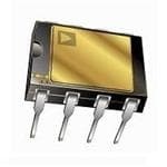
| 描述 | IC ACCELEROMETR DUAL-AXIS 8SBDIP加速计 Prec +/-5g Dual-Axis High Temp |
| 产品分类 | 加速计运动与定位传感器 |
| 品牌 | Analog Devices Inc |
| 产品手册 | |
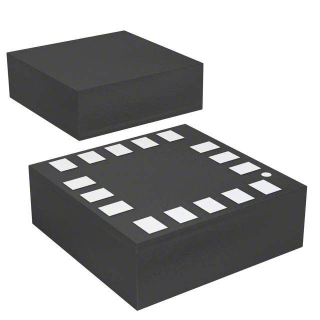
| 产品图片 |
|
| rohs | RoHS 合规性豁免无铅 / 符合限制有害物质指令(RoHS)规范要求 |
| 产品系列 | 加速计,Analog Devices ADXL206HDZiMEMS® |
| 数据手册 | |
| 产品型号 | ADXL206HDZ |
| PCN组件/产地 | |
| 产品种类 | 加速计 |
| 传感轴 | Dual |
| 供应商器件封装 | 8-CSBDIP |
| 分辨率 | - |
| 加速 | 5 g |
| 加速度范围 | ±5g |
| 商标 | Analog Devices |
| 安装类型 | 通孔 |
| 安装风格 | SMD/SMT |
| 封装 | Tube |
| 封装/外壳 | 8-CDIP(0.300",7.62mm) |
| 封装/箱体 | SBDIP-8 |
| 工厂包装数量 | 35 |
| 带宽 | 2.5kHz |
| 接口 | - |
| 数字输出-位数 | - |
| 数字输出-总线接口 | - |
| 最大工作温度 | + 175 C |
| 最小工作温度 | - 40 C |
| 标准包装 | 1 |
| 灵敏度 | 312mV/g |
| 电压-电源 | 4.75 V ~ 5.25 V |
| 电源电压-最大 | 5.25 V |
| 电源电压-最小 | 4.75 V |
| 电源电流 | 0.7 uA |
| 系列 | ADXL206 |
| 视频文件 | http://www.digikey.cn/classic/video.aspx?PlayerID=1364138032001&width=640&height=505&videoID=2245193160001http://www.digikey.cn/classic/video.aspx?PlayerID=1364138032001&width=640&height=505&videoID=2245193171001http://www.digikey.cn/classic/video.aspx?PlayerID=1364138032001&width=640&height=505&videoID=2245193161001http://www.digikey.cn/classic/video.aspx?PlayerID=1364138032001&width=640&height=505&videoID=2245193172001 |
| 轴 | X,Y |
| 输出类型 | 模拟 |


- 商务部:美国ITC正式对集成电路等产品启动337调查
- 曝三星4nm工艺存在良率问题 高通将骁龙8 Gen1或转产台积电
- 太阳诱电将投资9.5亿元在常州建新厂生产MLCC 预计2023年完工
- 英特尔发布欧洲新工厂建设计划 深化IDM 2.0 战略
- 台积电先进制程称霸业界 有大客户加持明年业绩稳了
- 达到5530亿美元!SIA预计今年全球半导体销售额将创下新高
- 英特尔拟将自动驾驶子公司Mobileye上市 估值或超500亿美元
- 三星加码芯片和SET,合并消费电子和移动部门,撤换高东真等 CEO
- 三星电子宣布重大人事变动 还合并消费电子和移动部门
- 海关总署:前11个月进口集成电路产品价值2.52万亿元 增长14.8%


PDF Datasheet 数据手册内容提取
Precision, ±5 g, Dual-Axis, High Temperature iMEMS Accelerometer Data Sheet ADXL206 FEATURES GENERAL DESCRIPTION High performance, dual-axis accelerometer The ADXL206 is a precision, low power, complete dual-axis on a single IC iMEMS® accelerometer for use in high temperature environ- −40°C to +175°C ambient temperature range ments. The accelerometer integrates the sensor with signal Long life: guaranteed 1000 hours at TA = 175°C conditioned voltage outputs on a single, monolithic IC. 13 mm × 8 mm × 2 mm side-brazed ceramic dual in-line The ADXL206 measures acceleration with a full-scale range package of ±5 g. The ADXL206 can measure both dynamic acceleration 1 mg resolution at 60 Hz (for example, vibration) and static acceleration (for example, Low power: 700 µA at V = 5 V (typical) S gravity). High zero g bias repeatability High sensitivity accuracy The typical noise floor is 110 μg/√Hz, allowing signals below Bandwidth adjustment with a single capacitor 1 mg (0.06° of inclination) to be resolved in tilt sensing appli- Single-supply operation cations using narrow bandwidths (<60 Hz). RoHS-compliant The user selects the bandwidth of the accelerometer using Compatible with Sn/Pb and Pb-free solder processes Capacitors C and C at the X and Y pins, respectively. X Y OUT OUT APPLICATIONS Bandwidths of 0.5 Hz to 2.5 kHz can be selected to suit the application. Geological exploration tilt and vibration measurement Extreme high temperature industrial products The ADXL206 is available in a 13 mm × 8 mm × 2 mm, 8-lead, side-brazed ceramic dual in-line package (SBDIP). FUNCTIONAL BLOCK DIAGRAM +5V VS ADXL206 CDC AAMCP DEMOD OUATMPPUT OUATMPPUT SENSOR RFILT RFILT 32kΩ 32kΩ COM ST YOUT XOUT CY CX 09600-001 Figure 1. Rev. B Document Feedback Information furnished by Analog Devices is believed to be accurate and reliable. However, no responsibility is assumed by Analog Devices for its use, nor for any infringements of patents or other One Technology Way, P.O. Box 9106, Norwood, MA 02062-9106, U.S.A. rights of third parties that may result from its use. Specifications subject to change without notice. No license is granted by implication or otherwise under any patent or patent rights of Analog Devices. Tel: 781.329.4700 ©2011–2015 Analog Devices, Inc. All rights reserved. Trademarks and registered trademarks are the property of their respective owners. Technical Support www.analog.com
ADXL206 Data Sheet TABLE OF CONTENTS Features .............................................................................................. 1 Performance ...................................................................................9 Applications ....................................................................................... 1 Applications Information .............................................................. 10 General Description ......................................................................... 1 Power Supply Decoupling ......................................................... 10 Functional Block Diagram .............................................................. 1 Setting the Bandwidth Using C and C ................................. 10 X Y Revision History ............................................................................... 2 Self-Test ....................................................................................... 10 Specifications ..................................................................................... 3 Design Trade-Offs for Selecting Filter Characteristics: Absolute Maximum Ratings ............................................................ 4 Noise/Bandwidth Trade-Off ........................................................ 10 Thermal Resistance ...................................................................... 4 Using the ADXL206 with Operating Voltages Other Than 5 V ................................................................................................ 11 ESD Caution .................................................................................. 4 Using the ADXL206 As a Dual-Axis Tilt Sensor ................... 11 Pin Configuration and Function Descriptions ............................. 5 Outline Dimensions ....................................................................... 12 Typical Performance Characteristics ............................................. 6 Ordering Guide .......................................................................... 12 Theory of Operation ........................................................................ 9 REVISION HISTORY 4/15—Rev. A to Rev. B Changes to Note 3, Table 1 .............................................................. 3 1/14—Rev. 0 to Rev. A Changes to Figure 3 .......................................................................... 5 4/11—Revision 0: Initial Version Rev. B | Page 2 of 12
Data Sheet ADXL206 SPECIFICATIONS T = −40°C to +175°C, V = 5 V, C = 0.1 μF, acceleration = 0 g, unless otherwise noted.1 A S X Table 1. Parameter Test Conditions/Comments Min Typ Max Unit SENSOR INPUT Each axis Measurement Range2 ±5 g Nonlinearity ±0.2 % FS Package Alignment Error ±1 Degrees Alignment Error X sensor to Y sensor ±0.1 Degrees Cross-Axis Sensitivity ±1.5 % SENSITIVITY (RATIOMETRIC)3 Sensitivity at X , Y V = 5 V 296 312 328 mV/g OUT OUT S Sensitivity Change Due to Temperature4 V = 5 V ±0.3 % S ZERO g BIAS LEVEL (RATIOMETRIC) 0 g Voltage at X , Y V = 5 V, T = 25°C 2.5 ± 0.025 V OUT OUT S A 0 g Bias Repeatability −40°C ≤ T ≤ +175°C ±10 mg A NOISE PERFORMANCE Noise Density V = 5 V, T = 25°C 110 µg/√Hz rms S A FREQUENCY RESPONSE5 C , C Range6 0.002 10 µF X Y R Tolerance 24 32 40 kΩ FILT Sensor Resonant Frequency 5.5 kHz SELF-TEST7 Logic Input Low 1 V Logic Input High 4 V ST Input Resistance to Ground 30 50 kΩ Output Change at X , Y ST pin Logic 0 to Logic 1 150 250 350 mV OUT OUT OUTPUT AMPLIFIER No load Output Swing Low 0.05 0.2 V Output Swing High 4.5 V LIFESPAN Usable Life Expectancy T = 175°C 1000 Hours A POWER SUPPLY Operating Voltage Range 4.75 5.25 V Supply Current 0.7 1.5 mA Turn-On Time8 20 ms 1 Minimum and maximum specifications are guaranteed. Typical specifications are not guaranteed. 2 Guaranteed by measurement of initial offset and sensitivity. 3 Sensitivity is essentially ratiometric to VS. 4 Defined as the output change from ambient temperature to maximum temperature or from ambient temperature to minimum temperature. 5 Actual frequency response controlled by user-supplied external capacitors (CX, CY). 6 Bandwidth = 1/(2 × π × 32 kΩ × C). For CX, CY = 0.002 µF, bandwidth = 2500 Hz. For CX, CY = 10 µF, bandwidth = 0.5 Hz. Minimum/maximum values are not tested. 7 Self-test response changes cubically with VS. 8 Larger values of CX, CY increase turn-on time. Turn-on time is approximately 160 × CX or CY + 4 ms, where CX and CY are in microfarads (µF). Rev. B | Page 3 of 12
ADXL206 Data Sheet ABSOLUTE MAXIMUM RATINGS THERMAL RESISTANCE Table 2. Parameter Rating θ is specified for the worst-case conditions, that is, for a device JA Acceleration (Any Axis) soldered in a printed circuit board (PCB) for surface-mount Unpowered 500 g packages. Powered 500 g Table 3. Thermal Resistance V −0.3 V to +7.0 V S Package Type θ θ Unit All Other Pins (COM − 0.3 V) to (V + 0.3 V) JA JC S 8-Lead SBDIP 120 20 °C/W Output Short-Circuit Duration Indefinite (Any Pin to Common) Ambient Operating Temperature −55°C to +175°C ESD CAUTION Range (T ) A Storage Temperature Range −65°C to +200°C Stresses at or above those listed under Absolute Maximum Ratings may cause permanent damage to the product. This is a stress rating only; functional operation of the product at these or any other conditions above those indicated in the operational section of this specification is not implied. Operation beyond the maximum operating conditions for extended periods may affect product reliability. CRITICAL ZONE TP tP TL TO TP RAMP-UP URETL TSMAX tL T A R PE TSMIN M E T PREtHSEAT RAMP-DOWN TIME25°C TO PEAKTIME 09600-002 Figure 2. Recommended Soldering Profile Table 4. Recommended Soldering Profile Limits Profile Feature Sn63/Pb37 Pb-Free Average Ramp Rate (T to T) 3°C/sec max 3°C/sec max L P Preheat Minimum Temperature (T ) 100°C 150°C SMIN Maximum Temperature (T ) 150°C 200°C SMAX Time (T to T ), t 60 sec to 120 sec 60 sec to 150 sec SMIN SMAX S Ramp-Up Rate (T to T) 3°C/sec max 3°C/sec max SMAX L Time Maintained Above Liquidous (t) 60 sec to 150 sec 60 sec to 150 sec L Liquidous Temperature (T) 183°C 217°C L Peak Temperature (T) 240°C + 0°C/−5°C 260°C + 0°C/−5°C P Time Within 5°C of Actual Peak Temperature (t) 10 sec to 30 sec 20 sec to 40 sec P Ramp-Down Rate (T to T) 6°C/sec max 6°C/sec max P L Time 25°C to Peak Temperature 6 minutes max 8 minutes max Rev. B | Page 4 of 12
Data Sheet ADXL206 PIN CONFIGURATION AND FUNCTION DESCRIPTIONS COM 1 +Y +X 8 ST NC 2 7 VS2 ADXL206 COM 3 TOP VIEW 6 VS YOUT 4 (Not to Scale) 5 XOUT NCCO N=N NEOC TC OTONN TEHCIST .P DINO. NOT 09600-003 Figure 3. Pin Configuration Table 5. Pin Function Descriptions Pin No. Mnemonic Description 1, 3 COM Common. 2 NC No Connect. Do not connect to this pin. 4 Y Y Channel Output. OUT 5 X X Channel Output. OUT 6 V Supply. S 7 V2 Supply. Must be connected to V. S S 8 ST Self-Test. Rev. B | Page 5 of 12
ADXL206 Data Sheet TYPICAL PERFORMANCE CHARACTERISTICS V = 5 V, unless otherwise noted. S 60 70 60 50 %) %) ON ( ON ( 50 TI 40 TI A A L L U U 40 P P O 30 O P P OF OF 30 T T N 20 N E E C C 20 R R E E P P 10 10 0 0 2.43 2.44 2.45 2.46 2.47 2.48VO2.49LTA2.50GE2.51 (V)2.52 2.53 2.54 2.55 2.56 2.57 09600-004 2.43 2.44 2.45 2.46 2.47 2.48VO2.49LTA2.50GE2.51 (V)2.52 2.53 2.54 2.55 2.56 2.57 09600-007 Figure 4. X-Axis Zero g Bias at TA = 25°C Figure 7. Y-Axis Zero g Bias at TA = 25°C 25 25 %) 20 %) 20 N ( N ( O O TI TI A A L 15 L 15 U U P P O O P P F F T O 10 T O 10 N N E E C C R R E E P 5 P 5 0 0 –1.2 –1.0 –0.8TEM–0.6PER–0.4ATUR–0.2E CO0EFFI0.2CIEN0.4T (mg0.6/°C)0.8 1.0 1.2 09600-005 –1.2 –1.0 –0.8TEM–0.6PER–0.4ATUR–0.2E CO0EFFI0.2CIEN0.4T (mg0.6/°C)0.8 1.0 1.2 09600-008 Figure 5. X-Axis Zero g Bias Temperature Coefficient Figure 8. Y-Axis Zero g Bias Temperature Coefficient 90 80 80 70 %) 70 %) N ( N ( 60 O O TI 60 TI A A 50 L L PU 50 PU PO PO 40 F 40 F O O T T 30 N 30 N E E C C R R 20 E 20 E P P 10 10 0 0 0.287 0.297 0.307 0.317 SE0.327NSITIV0.337ITY (V0.347/g) 0.357 0.367 0.377 0.387 09600-006 0.287 0.297 0.307 0.317 SE0.327NSITIV0.337ITY (V0.347/g) 0.357 0.367 0.377 0.387 09600-009 Figure 6. X-Axis Sensitivity at TA = 25°C Figure 9. Y-Axis Sensitivity at TA = 25°C Rev. B | Page 6 of 12
Data Sheet ADXL206 40 40 35 35 %) 30 %) 30 N ( N ( O O ATI 25 ATI 25 L L U U P P O 20 O 20 P P F F T O 15 T O 15 N N E E RC 10 RC 10 E E P P 5 5 0–5 –4 –3 C–2ROS–S1-AXIS0 RESP1ONSE2 (%) 3 4 5 09600-010 0–5 –4 –3 C–2ROS–S1-AXIS0 RESP1ONSE2 (%) 3 4 5 09600-011 Figure 10. Cross-Axis Response, Z-Axis vs. X-Axis Figure 13. Cross-Axis Response, Z-Axis vs. Y-Axis 325 325 320 320 g) g) V/ V/ m315 m315 Y ( Y ( T T VI VI TI TI SI310 SI310 N N E E S S 305 305 30–0100 –50 AMB0IENT TEM5P0ERATUR1E0 0(°C) 150 200 09600-016 30–0100 –50 AMB0IENT TEM5P0ERATUR1E0 0(°C) 150 200 09600-017 Figure 11. X-Axis Sensitivity over Temperature, Nine Devices Figure 14. Y-Axis Sensitivity over Temperature, Nine Devices 100 75 Y-AXIS 5V INPUT 50 V) 25 m T ( 0 V) OUTPUT AS DRIF––2550 E (1V/DI UT BI–75 LTAG TP–100 X-AXIS VO U O–125 0V –150 –175 –200–50 –25 0 A2M5BIEN5T0 TEM7P5ERA1T0U0RE 1(2°C5) 150 175 200 09600-015 TIME (2ms/DIV) 09600-014 Figure 12. Zero g Output Bias Drift over Temperature, Eight Devices Figure 15. Turn-On Time, CX, CY = 0.1 μF, Time Scale = 2 ms/div Rev. B | Page 7 of 12
ADXL206 Data Sheet 25 25 %) %) N ( 20 N (20 O O TI TI A A L L PU 15 PU15 O O P P F F O O NT 10 NT 10 E E C C R R E E P 5 P 5 0–40 –30 –O2U0TPUT –B1I0AS DRIF0T (mV) 10 20 09600-018 0 –20 OUTPU–1T0 BIAS DRIFT 0(mV) 10 09600-019 Figure 16. X-Axis Zero g Output Bias Drift over 1000 Hours Figure 18. Y-Axis Zero g Output Bias Drift over 1000 Hours at TA = 175°C, Powered at TA = 175°C, Powered 100 0.9 90 VS = 5V VS = 5V 0.8 %) 80 N ( O 70 TI 0.7 ULA 60 mA) F POP 50 RENT ( 0.6 CENT O 4300 CUR 0.5 R E P 20 0.4 10 0 0.3 200 300 400 C50U0RREN60T0 (µA)700 800 900 1000 09600-013 –50 0AMBIENT TEM5P0ERATURE (°C1)00 150 09600-012 Figure 17. Supply Current at TA = 25°C Figure 19. Supply Current vs. Temperature Rev. B | Page 8 of 12
Data Sheet ADXL206 THEORY OF OPERATION The ADXL206 is a complete acceleration measurement system The output of the demodulator is amplified and brought off chip on a single, monolithic IC. The part contains a polysilicon, surface- through a 32 kΩ resistor. At this point, the user can set the signal micromachined sensor and signal conditioning circuitry to imple- bandwidth of the device by adding a capacitor. This filtering ment an open-loop acceleration measurement architecture. The improves measurement resolution and helps prevent aliasing. output signals are analog voltages proportional to acceleration. PERFORMANCE The ADXL206 is capable of measuring both positive and negative Rather than using additional temperature compensation circuitry, accelerations to at least ±5 g. The accelerometer can measure innovative design techniques have been used to ensure that high static acceleration forces such as gravity, allowing it to be used performance is built in. As a result, there is essentially no quantiza- as a tilt sensor. tion error or nonmonotonic behavior, and temperature hysteresis The sensor is a surface-micromachined, polysilicon structure is very low (typically less than 2 mg over the −40°C to +175°C built on top of the silicon wafer. Polysilicon springs suspend the temperature range). structure over the surface of the wafer and provide resistance Figure 12 shows the 0 g output performance of eight parts over against acceleration forces. Deflection of the structure is measured the −40°C to +175°C temperature range. using a differential capacitor that consists of independent fixed plates and plates attached to the moving mass. The fixed plates Figure 11 and Figure 14 show the typical sensitivity shift over are driven by 180° out-of-phase square waves. Acceleration deflects temperature for V = 5 V. Sensitivity stability is optimized for S the beam and unbalances the differential capacitor, resulting in V = 5 V, but it is very good over the full supply voltage range. S an output square wave whose amplitude is proportional to accel- eration. Phase-sensitive demodulation techniques are then used to rectify the signal and determine the direction of the acceleration. Rev. B | Page 9 of 12
ADXL206 Data Sheet APPLICATIONS INFORMATION POWER SUPPLY DECOUPLING DESIGN TRADE-OFFS FOR SELECTING FILTER CHARACTERISTICS: NOISE/BANDWIDTH TRADE-OFF For most applications, a single 0.1 µF capacitor, C , adequately DC decouples the accelerometer from noise on the power supply. In The accelerometer bandwidth selected ultimately determines some cases, however, particularly where noise is present at the the measurement resolution (smallest detectable acceleration). 140 kHz internal clock frequency (or any harmonic thereof), Filtering can be used to lower the noise floor, improving the noise on the supply can cause interference on the ADXL206 resolution of the accelerometer. Resolution is dependent on the output. If additional decoupling is needed, a 100 Ω (or smaller) analog filter bandwidth at X . OUT resistor or ferrite bead can be inserted in the supply line of the The output of the ADXL206 has a typical bandwidth of 2.5 kHz. ADXL206. Additionally, a larger bulk bypass capacitor (in the The user must filter the signal at this point to limit aliasing 1 µF to 22 µF range) can be added in parallel to C . DC errors. The analog bandwidth must be no more than half the SETTING THE BANDWIDTH USING CX AND CY analog-to-digital sampling frequency to minimize aliasing. The analog bandwidth can be further decreased to reduce noise and The ADXL206 has provisions for band-limiting the X and OUT improve resolution. Y pins. A capacitor must be added to the pin to implement OUT low-pass filtering for antialiasing and noise reduction. The The ADXL206 noise has the characteristics of white Gaussian noise, equation for the 3 dB bandwidth is which contributes equally at all frequencies and is described in terms of µg/√Hz (that is, the noise is proportional to the square root f = 1/(2π(32 kΩ) × C) −3 dB x of the accelerometer bandwidth). The user should limit bandwidth or more simply, to the lowest frequency needed by the application to maximize f−3 dB = 5 µF/Cx the resolution and dynamic range of the accelerometer. The tolerance of the internal resistor (RFILT) can vary typically With the single-pole roll-off characteristic, the typical noise of as much as ±25% of its nominal value (32 kΩ); thus, the band- the ADXL206 is determined by width varies accordingly. A minimum capacitance of 2000 pF ( ) ( ) rms Noise = 110µg/ Hz × BW × 1.6 for C and C is required in all cases. X Y At 100 Hz, the noise is Table 6. Filter Capacitor Selection, C and C X Y ( ) ( ) Bandwidth (Hz) Capacitor (µF) rms Noise = 110µg/ Hz × 100 × 1.6 = 1.4mg 1 4.7 Often, the peak value of the noise is desired. Peak-to-peak noise 10 0.47 can only be estimated by statistical methods. Table 7 is useful 50 0.10 for estimating the probability of exceeding various peak values, 100 0.05 given the rms value. 200 0.027 500 0.01 Table 7. Estimation of Peak-to-Peak Noise % of Time That Noise Exceeds SELF-TEST Peak-to-Peak Value Nominal Peak-to-Peak Value 2 × rms 32 The ST pin controls the self-test feature. When this pin is set to 4 × rms 4.6 V, an electrostatic force is exerted on the beam of the acceler- S 6 × rms 0.27 ometer. The resulting movement of the beam allows the user to 8 × rms 0.006 test whether the accelerometer is functional. The typical change in output is 800 mg (corresponding to 250 mV). This pin can be Peak-to-peak noise values give the best estimate of the uncer- left open-circuit or connected to common in normal use. tainty in a single measurement; peak-to-peak noise is estimated by 6 × rms. Table 8 gives the typical noise output of the ADXL206 The ST pin should never be exposed to voltage greater than for various C and C values. V + 0.3 V. If the system design is such that this condition X Y S cannot be guaranteed (that is, multiple supply voltages are Table 8. Typical Noise Output for Various Capacitor Values present), it is recommended that a clamping diode with low C , C RMS Noise Peak-to-Peak Noise X Y forward voltage be connected between ST and VS. Bandwidth (Hz) (µF) (mg) Estimate (mg) 10 0.47 0.4 2.6 50 0.1 1.0 6 100 0.047 1.4 8.4 500 0.01 3.1 18.7 Rev. B | Page 10 of 12
Data Sheet ADXL206 USING THE ADXL206 WITH OPERATING VOLTAGES USING THE ADXL206 AS A DUAL-AXIS TILT OTHER THAN 5 V SENSOR The ADXL206 is tested and specified at V = 5 V; however, it One of the most popular applications of the ADXL206 is tilt S can be powered with V as low as 3 V or as high as 6 V. Some measurement. An accelerometer uses the force of gravity as an S performance parameters change as the supply voltage is varied. input vector to determine the orientation of an object in space. The ADXL206 output is ratiometric; therefore, the output An accelerometer is most sensitive to tilt when its sensitive axis sensitivity (or scale factor) varies proportionally to the supply is perpendicular to the force of gravity, that is, parallel to the voltage. The zero g bias output is also ratiometric; therefore, the earth’s surface. At this orientation, the sensitivity of the acceler- zero g output is nominally equal to V/2 at all supply voltages. ometer to changes in tilt is highest. When the axis of sensitivity S is parallel to gravity, that is, near its +1 g or −1 g reading, the The output noise is not ratiometric but is absolute in volts; change in output acceleration per degree of tilt is negligible. therefore, the noise density decreases as the supply voltage When the accelerometer is perpendicular to gravity, its output increases. changes nearly 17.5 mg per degree of tilt. At 45°, its output Self-test response in g is roughly proportional to the square of changes at only 12.2 mg per degree and resolution declines. the supply voltage. However, when ratiometricity of sensitivity Dual-Axis Tilt Sensor: Converting Acceleration to Tilt is factored in with supply voltage, self-test response in volts is roughly proportional to the cube of the supply voltage. There- When the accelerometer is oriented so that both its x-axis and fore, at V = 3 V, the typical self-test response is approximately y-axis are parallel to the earth’s surface, it can be used as a 2-axis S 50 mV or about 160 mg. tilt sensor with a roll axis and a pitch axis. After the output signal from the accelerometer is converted to an acceleration that varies between −1 g and +1 g, the output tilt in degrees is calculated as follows: PITCH = arcsin(A /1 g) X ROLL = arcsin(A /1 g) Y Make sure to account for overranges. It is possible for the accelerometer to output a signal greater than ±1 g due to vibration, shock, or other accelerations. Rev. B | Page 11 of 12
ADXL206 Data Sheet OUTLINE DIMENSIONS 0.528 0.520 0.512 8 5 0.298 0.290 0.320 0.282 0.310 0.300 1 4 INDEX 0.305 0.125 MARK 0.300 0.110 0.295 0.095 0.011 0.010 0.105 0.009 0.095 0.130NOM 0.085 0.045 SEATING 0.035 0.011 PLANE 0.054 0.025 0.010 NOM 0.310 0.009 0.175NOM 0.020 0.300 0.105 0.018 0.290 0.100 0.095 0N.O03M2 0.016 07-08-2010-B Figure 20. 8-Lead Side-Brazed Ceramic Dual In-Line Package [SBDIP] (D-8-1) Dimensions shown in inches ORDERING GUIDE Model1, 2 Number of Axes Specified Voltage (V) Temperature Range Package Description Package Option ADXL206HDZ 2 5 −40°C to +175°C 8-Lead SBDIP D-8-1 1 Lead finish. Gold over nickel over tungsten. 2 Z = RoHS Compliant Part. ©2011–2015 Analog Devices, Inc. All rights reserved. Trademarks and registered trademarks are the property of their respective owners. D09600-0-4/15(B) Rev. B | Page 12 of 12
Mouser Electronics Authorized Distributor Click to View Pricing, Inventory, Delivery & Lifecycle Information: A nalog Devices Inc.: ADXL206HDZ