ICGOO在线商城 > 隔离器 > 隔离器 - 栅极驱动器 > ADUM5230ARWZ
 Datasheet下载
- 型号: ADUM5230ARWZ
- 制造商: Analog
- 库位|库存: xxxx|xxxx
- 要求:
| 数量阶梯 | 香港交货 | 国内含税 |
| +xxxx | $xxxx | ¥xxxx |
查看当月历史价格
查看今年历史价格
ADUM5230ARWZ产品简介:
ICGOO电子元器件商城为您提供ADUM5230ARWZ由Analog设计生产,在icgoo商城现货销售,并且可以通过原厂、代理商等渠道进行代购。 ADUM5230ARWZ价格参考。AnalogADUM5230ARWZ封装/规格:隔离器 - 栅极驱动器, Gate Driver Magnetic Coupling 2500Vrms 2 Channel 16-SOIC。您可以下载ADUM5230ARWZ参考资料、Datasheet数据手册功能说明书,资料中有ADUM5230ARWZ 详细功能的应用电路图电压和使用方法及教程。
ADUM5230ARWZ是Analog Devices Inc.推出的一款双通道隔离式栅极驱动器,广泛应用于需要高可靠性电气隔离和高效功率开关控制的场景。其主要应用场景包括工业电机驱动、开关电源(SMPS)、逆变器、新能源发电系统(如太阳能逆变器和风能转换系统)以及电动汽车充电设备等。

该器件集成了iCoupler®数字隔离技术与DC/DC转换器,可为次级侧提供隔离电源,简化了系统设计并减少了外部元件数量。两个输出通道均具有高噪声抑制能力,适用于高电压、高噪声工业环境。由于具备高达5A的峰值输出电流和快速传播延迟特性,ADUM5230ARWZ能够高效驱动MOSFET、IGBT等功率器件,确保开关动作精确可靠。

此外,它在绝缘耐压方面表现优异,隔离电压可达5000 V RMS,符合增强型隔离安全标准,适合用于对安全性要求较高的工业自动化和电力控制系统。其工作温度范围宽(-40°C至+125°C),可在严苛环境下稳定运行。综上,ADUM5230ARWZ特别适用于需集成隔离电源、紧凑设计且高性能的功率驱动应用。
| 参数 | 数值 |
| 产品目录 | |
| ChannelType | 单向 |
| 描述 | OPTOISO 2.5KV 2CH DRIVER 16SOIC数字隔离器 Half-Bridge Dvr w/ Intg Hi-Side Supply |
| 产品分类 | 光隔离器 - 栅极驱动器集成电路 - IC |
| IsolatedPower | 无 |
| 品牌 | Analog Devices |
| 产品手册 | |
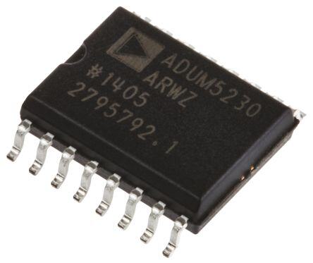
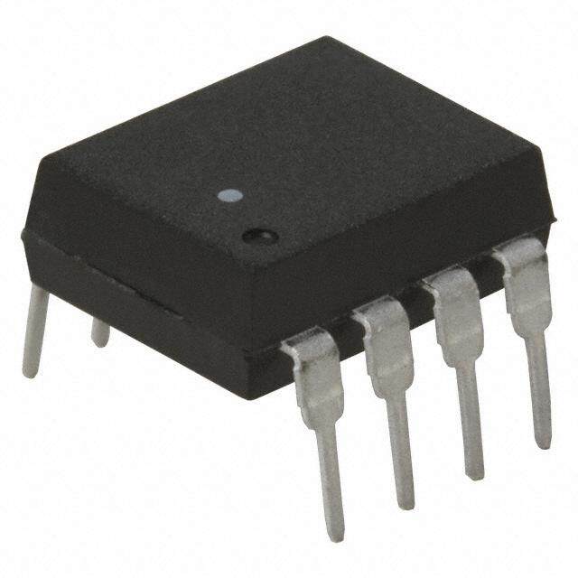
| 产品图片 |
|
| rohs | 符合RoHS无铅 / 符合限制有害物质指令(RoHS)规范要求 |
| 产品系列 | 接口 IC,数字隔离器,Analog Devices ADUM5230ARWZiCoupler® |
| 数据手册 | |
| 产品型号 | ADUM5230ARWZ |
| PulseWidthDistortion(Max) | 8ns |
| 上升/下降时间(典型值) | 25ns, 10ns (最小值) |
| 不同If时的传播延迟高-低 | 100ns |
| 产品目录页面 | |
| 产品种类 | |
| 传播延迟tpLH/tpHL(最大值) | 100ns, 100ns |
| 传播延迟时间 | 100 ns |
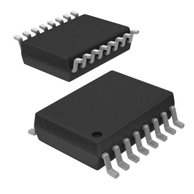
| 供应商器件封装 | 16-SOIC W |
| 共模瞬态抗扰度(最小值) | 25kV/µs |
| 其它图纸 |
|
| 功率耗散 | 150 mW |
| 包装 | 管件 |
| 商标 | Analog Devices |
| 安装类型 | 表面贴装 |
| 安装风格 | SMD/SMT |
| 封装 | Tube |
| 封装/外壳 | 16-SOIC(0.295",7.50mm 宽) |
| 封装/箱体 | SOIC-16 |
| 工作温度 | -40°C ~ 105°C |
| 工厂包装数量 | 47 |
| 技术 | 磁耦合 |
| 数据速率 | 1MHz |
| 最大工作温度 | + 105 C |
| 最小工作温度 | - 40 C |
| 标准包装 | 47 |
| 电压-正向(Vf)(典型值) | - |
| 电压-电源 | 4.5 V ~ 5.5 V, 12 V ~ 18.5 V |
| 电压-隔离 | 2500Vrms |
| 电流-DC正向(If) | - |
| 电流-峰值输出 | - |
| 电流-输出/通道 | - |
| 电流-输出高,低 | - |
| 电源电压-最小 | 4.5 V, 12 V |
| 电源电流 | 200 mA |
| 类型 | General Purpose |
| 系列 | ADUM5230 |
| 绝缘电压 | 2.5 kVrms |
| 脉宽失真(最大) | 8ns |
| 视频文件 | http://www.digikey.cn/classic/video.aspx?PlayerID=1364138032001&width=640&height=505&videoID=2219593469001http://www.digikey.cn/classic/video.aspx?PlayerID=1364138032001&width=640&height=505&videoID=2219593470001http://www.digikey.cn/classic/video.aspx?PlayerID=1364138032001&width=640&height=505&videoID=2219614223001 |
| 认可 | UR |
| 输入-输入侧1/输入侧2 | 2/0 |
| 输入类型 | - |
| 输出类型 | 栅极驱动器 |
| 通道数 | 2 |
| 通道数量 | 2 Channel |


- 商务部:美国ITC正式对集成电路等产品启动337调查
- 曝三星4nm工艺存在良率问题 高通将骁龙8 Gen1或转产台积电
- 太阳诱电将投资9.5亿元在常州建新厂生产MLCC 预计2023年完工
- 英特尔发布欧洲新工厂建设计划 深化IDM 2.0 战略
- 台积电先进制程称霸业界 有大客户加持明年业绩稳了
- 达到5530亿美元!SIA预计今年全球半导体销售额将创下新高
- 英特尔拟将自动驾驶子公司Mobileye上市 估值或超500亿美元
- 三星加码芯片和SET,合并消费电子和移动部门,撤换高东真等 CEO
- 三星电子宣布重大人事变动 还合并消费电子和移动部门
- 海关总署:前11个月进口集成电路产品价值2.52万亿元 增长14.8%

PDF Datasheet 数据手册内容提取
Isolated Half-Bridge Driver with Integrated High-Side Supply Data Sheet ADuM5230 FEATURES FUNCTIONAL BLOCK DIAGRAM Integrated, isolated high-side supply 150 mW of secondary side power GND1 1 ISOLATED 16 VOA DC-TO-DC Isolated high-side and low-side outputs CONVERTER VDD1 2 15 VISO 100 mA output source current, 300 mA output sink current High common-mode transient immunity: >25 kV/μs VADJ 3 14 GNDISO High temperature operation: 105°C Adjustable power level GND1 4 13 DNC Wide body, 16-lead SOIC package Safety and regulatory approvals VIA 5 ╓╜ ENCODE DECODE ╓╜ 12 DNC UL recognition: 2500 V rms for 1 minute per UL1577 Qualified for automotive applications VIB 6 ╓╜ ENCODE DECODE ╓╜ 11 GNDB APPLICATIONS VDD1 7 10 VDDB ADuM5230 MAMuOottSooFmrE doTrt/iiIvvGeeBs T gate drives GDNNDC 1= D8O NOT CONNECT. DO NOT CONNECTTO THIS PIN. 9 VOB 07080-001 Figure 1. Power supplies GENERAL DESCRIPTION The ADuM52301 is an isolated half-bridge gate driver that In comparison to gate drivers employing high voltage level employs Analog Devices, Inc., iCoupler® technology to provide translation methodologies, the ADuM5230 offers the benefit independent and isolated high-side and low-side outputs. of true, galvanic isolation between the input and each output. Combining CMOS and microtransformer technologies, this Each output can operate up to ±700 V relative to the input, P isolation component contains an integrated dc-to-dc converter thereby supporting low-side switching to negative voltages. providing an isolated high-side supply. This eliminates the cost, The differential voltage between the high side and low side space, and performance difficulties associated with external may be as high as 700 V . P supply configurations such as bootstrap circuitry. This high- side isolated supply powers not only the ADuM5230 high-side output but also any external buffer circuitry used with the ADuM5230. 1 Protected by U.S. Patents 5,952,849; 6,873,065; 6,903,578; 7,075,329; other pending patents. Rev. C Document Feedback Information furnished by Analog Devices is believed to be accurate and reliable. However, no responsibility is assumed by Analog Devices for its use, nor for any infringements of patents or other One Technology Way, P.O. Box 9106, Norwood, MA 02062-9106, U.S.A. rights of third parties that may result from its use. Specifications subject to change without notice. No license is granted by implication or otherwise under any patent or patent rights of Analog Devices. Tel: 781.329.4700 ©2008–2015 Analog Devices, Inc. All rights reserved. Trademarks and registered trademarks are the property of their respective owners. Technical Support www.analog.com
ADuM5230 Data Sheet TABLE OF CONTENTS Features .............................................................................................. 1 Applications Information .............................................................. 10 Applications ....................................................................................... 1 Theory of Operation .................................................................. 10 Functional Block Diagram .............................................................. 1 Printed Circuit Board (PCB) Layout ....................................... 10 General Description ......................................................................... 1 Thermal Analysis ....................................................................... 10 Revision History ............................................................................... 2 Propagation Delay-Related Parameters ................................... 11 Specifications ..................................................................................... 3 DC Correctness and Magnetic Field Immunity........................... 11 Electrical Characteristics ............................................................. 3 Power Consumption .................................................................. 12 Package Characteristics ............................................................... 5 Increasing and Decreasing Available Power ............................... 12 Regulatory Information ............................................................... 5 Common-Mode Transient Immunity ..................................... 12 Insulation and Safety-Related Specifications ............................ 5 Typical Application Usage ......................................................... 13 Recommended Operating Conditions ...................................... 5 Insulation Lifetime ..................................................................... 14 Absolute Maximum Ratings ............................................................ 6 Outline Dimensions ....................................................................... 15 ESD Caution .................................................................................. 6 Ordering Guide .......................................................................... 15 Pin Configuration and Function Descriptions ............................. 7 Automotive Products ................................................................. 15 Typical Perfomance Characteristics ............................................... 8 REVISION HISTORY 12/15—Rev. B to Rev. C Changes to Table 1 ............................................................................ 3 Changes to Table 5 ............................................................................ 5 2/13—Rev. A to Rev. B Changes to Features and Applications Sections and Figure 1 .... 1 Added ADuM5230W DC Specifications ...................................... 3 Changes to Regulatory Information Section ................................ 5 Changes to Pin Configuration and Function Descriptions Section, Figure 3, and Table 8 ......................................................... 7 Change to Printed Circuit Board (PCB) Layout Section and Figure 15 .......................................................................................... 10 Change to Ordering Guide ............................................................ 15 Added Automotive Products Section........................................... 15 3/12—Rev. 0 to Rev. A Added Hyperlink for Safety and Regulatory Approvals Entry in Features Section ................................................................................ 1 Change to Printed Circuit Board (PCB) Layout Section .......... 10 Updated Outline Dimensions ....................................................... 15 4/08—Revision 0: Initial Version Rev. C | Page 2 of 15
Data Sheet ADuM5230 SPECIFICATIONS ELECTRICAL CHARACTERISTICS All voltages are relative to their respective ground. 4.5 V ≤ V ≤ 5.5 V, 12.0 ≤ V ≤ 18.0 V. All min/max specifications apply over the DD1 DDB entire recommended operating range, unless otherwise noted. All typical specifications are at T = 25°C, V = 5.0 V, V = 15 V. A DD1 DDB Table 1. Parameter Symbol Min Typ Max Unit Test Conditions/Comments DC SPECIFICATIONS Input Supply Current, Quiescent I 125 mA I = 0 mA, dc signal inputs, DD1 (Q) ISO V = open ADJ Channel B Supply Current, Quiescent I 1.6 mA DDB (Q) Channel A Output Supply Voltage V 12 15 18.5 V ISO At 0 kHz Switching Frequency Maximum Channel A Output Supply Current I 10 mA ISO (MAX, 0) At 100 kHz Switching Frequency Maximum Channel A Output Supply Current I 7.5 mA C = 200 pF ISO (MAX, 100) L Input Supply Current I 200 mA I = I DD1 ISO ISO (MAX, 100) Channel B Supply Current I 1.8 mA C = 200 pF DDB L At 1000 kHz Switching Frequency Maximum Channel A Output Supply Current I 5.0 mA C = 200 pF ISO (MAX, 1000) L Input Supply Current I 200 mA I = I DD1 ISO ISO (MAX, 1000) Channel B Supply Current I 7.5 mA C = 200 pF DDB L Input Currents I , I −10 +0.01 +10 µA 0 ≤ V , V ≤ 5.5 V IA IB IA IB Logic High Input Voltage V , V 0.7 × V V ATH BTH DD1 Logic Low Input Voltage V , V 0.3 × V V ATL BTL DD1 Logic High Output Voltages V , V V − 0.1, V , V V I , I = −1 mA OAH OBH ISO ISO DDB OA OB V − 0.1 DDB Logic Low Output Voltages V , V 0.1 V I , I = 1 mA OAL OBL OA OB Undervoltage Lockout, V and V Supply ISO DDB Positive-Going Threshold V 8.0 10.1 V DDBUV+ Negative-Going Threshold V 7.4 9.0 V DDBUV− Hysteresis V 0.9 V DDBUVH Undervoltage Lockout, V Supply DD1 Positive-Going Threshold V 3.5 4.2 V DD1UV+ Negative-Going Threshold V 3.0 3.9 V DD1UV− Hysteresis V 0.4 V DD1UVH Output Short-Circuit Pulsed Current, Sourcing1 I , I 100 mA OA OB Output Short-Circuit Pulsed Current, Sinking1 I , I 300 mA OA OB SWITCHING SPECIFICATIONS Minimum Pulse Width2 PW 100 ns C = 200 pF L Maximum Switching Frequency3 1 MHz C = 200 pF L Propagation Delay4 t , t 100 ns C = 200 pF PHL PLH L Change vs. Temperature 100 ps/°C Pulse Width Distortion, |t − t | PWD 8 ns C = 200 pF PLH PHL L Channel-to-Channel Matching, Rising or t 8 ns C = 200 pF M2 L Falling Matching Edge Polarity5 Channel-to-Channel Matching, Rising vs. t 10 ns C = 200 pF M1 L Falling Opposite Edge Polarity6 Rev. C | Page 3 of 15
ADuM5230 Data Sheet Parameter Symbol Min Typ Max Unit Test Conditions/Comments Part to Part Matching, Rising or Falling Edges7 55 ns C = 200 pF L Part to Part Matching, Rising vs. Falling Edges8 63 ns C = 200 pF L Common-Mode Transient Immunity at |CM | 25 35 kV/µs V = V , V = 1000 V, H Ix DD1 CM Logic High Output transient magnitude = 800 V Common-Mode Transient Immunity at |CM| 25 35 kV/µs V = 0 V, V = 1000 V, L Ix CM Logic Low Output transient magnitude = 800 V Output Rise Time (10% to 90%) t 25 ns C = 200 pF, I = 10 mA, R L ISO 100 kHz switching frequency Output Fall Time (10% to 90%) t 10 ns C = 200 pF, I = 10 mA, F L ISO 100 kHz switching frequency 1 Short-circuit duration is less than 1 sec. Average output current must conform to the limit shown under the Absolute Maximum Ratings section. 2 The minimum pulse width is the shortest pulse width at which the specified timing parameters are guaranteed. Operation below the minimum pulse width is strongly discouraged because in some instances pulse stretching to 1 µs may occur. 3 The maximum switching frequency is the maximum signal frequency at which the specified timing and power conversion parameters are guaranteed. Operation above the maximum frequency is strongly discouraged. 4 tPHL propagation delay is measured from the 50% level of the falling edge of the VIx signal to the 50% level of the falling edge of the VOx signal. tPLH propagation delay is measured from the 50% level of the rising edge of the VIx signal to the 50% level of the rising edge of the VOx signal. 5 In channel-to-channel matching, the rising or falling matching edge polarity is the magnitude of the propagation delay difference between two channels of the same part when both inputs are either both rising or falling edges. The loads on each channel are equal. 6 In channel-to-channel matching, the rising vs. falling opposite edge polarity is the magnitude of the propagation delay difference between two channels of the same part when one input is a rising edge and one input is a falling edge. The loads on each channel are equal. 7 Part-to-part matching, rising or falling edges, is the magnitude of the propagation delay difference between the same channels of two different parts when the inputs are either both rising or falling edges. The supply voltages, temperatures, and loads of each part are equal. 8 Part-to-part matching, rising vs. falling edges, is the magnitude of the propagation delay difference between the same channels of two different parts when one input is a rising edge and the other input is a falling edge. The supply voltages, temperatures, and loads of each part are equal. Rev. C | Page 4 of 15
Data Sheet ADuM5230 PACKAGE CHARACTERISTICS Table 2. Parameter Symbol Min Typ Max Unit Test Conditions/Comments Resistance (Input to Output)1 R 1012 Ω I-O Capacitance (Input to Output)1 C 2.0 pF f = 1 MHz I-O Input Capacitance C 4.0 pF I IC Junction-to-Ambient Thermal Resistance θ 48 °C/W JA 1 The device is considered a two-terminal device: Pin 1 to Pin 8 are shorted together, and Pin 9 to Pin 16 are shorted together. REGULATORY INFORMATION The ADuM5230 is approved by the organization listed in Table 3. Table 3. UL1 Recognized under 1577 component recognition program, File E214100 1 In accordance with UL1577, each ADuM5230 is proof-tested by applying an insulation test voltage ≥ 3000 V rms for 1 sec (current leakage detection limit = 5 μA). INSULATION AND SAFETY-RELATED SPECIFICATIONS Table 4. Parameter Symbol Value Unit Test Conditions/Comments Rated Dielectric Insulation Voltage 2500 V rms 1-minute duration Minimum External Air Gap (Clearance) L(I01) 3.5 min mm Measured from input conductors to output conductors, shortest distance through air Minimum External Tracking (Creepage) L(I02) 3.5 min mm Measured from input conductors to output conductors, shortest distance path along body Minimum Internal Gap (Internal Clearance) 0.017 min mm Distance through the insulation Tracking Resistance (Comparative Tracking Index) CTI >175 V DIN IEC 112/VDE 0303 Part 1 Isolation Group IIIa Material Group (DIN VDE 0110, 1/89, Table 1) 600 RECOMMENDED OPERATING CONDITIONS mA) 500 Table 5. NT ( Parameter Value E URR 400 Operating Temperature (TA) −40°C to +105°C CD1 Input Supply Voltage1 (VDD1) 4.5 V to 5.5 V G VD300 Channel B Supply Voltage1 (VDDB) 12 V to 18.5 V N Input Signal Rise and Fall Times 1 ms TI RA 200 PE 1 All voltages are relative to their respective ground. O E F 100 A S 0–40 0 AMB4I0ENT TEM8P0ERATUR1E2 0(°C) 160 20007080-010 Figure 2. Thermal Derating Curve, Dependence of Safety Limiting Values on Case Temperature, per DIN EN 60747-5-2 Rev. C | Page 5 of 15
ADuM5230 Data Sheet ABSOLUTE MAXIMUM RATINGS Ambient temperature = 25°C, unless otherwise noted. Stresses at or above those listed under Absolute Maximum Ratings may cause permanent damage to the product. This is a Table 6. stress rating only; functional operation of the product at these Parameter Rating or any other conditions above those indicated in the operational Storage Temperature (T ) −55°C to +150°C ST section of this specification is not implied. Operation beyond Ambient Operating Temperature (T ) −40°C to +105°C A the maximum operating conditions for extended periods may Input Supply Voltage (V )1 −0.5 V to +7.0 V DD1 affect product reliability. Channel B Supply Voltage (V )1 −0.5 V to +27 V DDB Input Voltage (V , V )1 −0.5 V to V + 0.5 V IA IB DDI Output Voltage (V , V )1 −0.5 V to V + 0.5 V, OA OB ISO Table 7. Maximum Continuous Working Voltage1 −0.5 V to V + 0.5 V DDB Input-Output Voltage2 −700 V to +700 V Parameter Max Unit Constraint PEAK PEAK Output Differential Voltage3 700 V AC Voltage PEAK Output DC Current (IOA, IOB) −20 mA to +20 mA Bipolar Waveform 424 V peak 50-year minimum lifetime Common-Mode Transients4 −100 kV/µs to +100 kV/µs Unipolar Waveform 1 All voltages are relative to their respective ground. Basic Insulation 600 V peak 50-year minimum 2 Input-to-output voltage is defined as GNDISO − GND1 or GNDB − GND1. lifetime 34 OReufteprus tt od icfofemremntoinal- mvooltdaeg ter aisn dsieefnintse dac arso GssN aDnIySO i n−s GulNaDtioB.n barrier. Common- DC Voltage mode transients exceeding the Absolute Maximum Ratings may cause Basic Insulation 600 V peak 50-year minimum latch-up or permanent damage. lifetime 1 Refers to continuous voltage magnitude imposed across the isolation barrier. See the Insulation Lifetime section for more details. ESD CAUTION Rev. C | Page 6 of 15
Data Sheet ADuM5230 PIN CONFIGURATION AND FUNCTION DESCRIPTIONS GND1 1 16 VOA VDD1 2 15 VISO VADJ 3 ADuM5230 14 GNDISO GND1 4 TOP VIEW 13 DNC VIA 5 (Not to Scale) 12 DNC VIB 6 11 GNDB VDD1 7 10 VDDB GND1DN8C = DO NOT CONNE9CTVOB 07080-002 Figure 3. Pin Configuration Table 8. Pin Function Descriptions Pin No. Mnemonic Description 1 GND Ground Reference for Input Logic Signals. 1 2 V Input Supply Voltage, 4.5 V to 5.5 V. DD1 3 V Adjusts Internal DC-to-DC Converter Duty Cycle (Normally Left Unconnected). ADJ 4 GND Ground Reference for Input Logic Signals. 1 5 V Logic Input A. IA 6 V Logic Input B. IB 7 V Input Supply Voltage, 4.5 V to 5.5 V. DD1 8 GND Ground Reference for Input Logic Signals. 1 9 V Output B Signal. OB 10 V Output B Supply Voltage, 12 V to 18 V. DDB 11 GND Ground Reference for Output B Signal. B 12 DNC Do Not Connect. 13 DNC Do Not Connect. 14 GND Ground Reference for Output A Signal and Isolated Output Supply Voltage. ISO 15 V Isolated Output Supply Voltage. ISO 16 V Output A Signal. OA For specific layout guidelines, refer to the AN-0971 Application Note, Recommendations for Control of Radiated Emissions with isoPower Devices. Table 9. Truth Table (Positive Logic) V Input1 V Input1 V State2 V State2 V State1, 2 V Output V Output Notes IA IB DD1 ISO DDB OA OB High High Powered Powered Powered High High High Low Powered Powered Powered High Low Low High Powered Powered Powered Low High Low Low Powered Powered Powered Low Low X X UVLO Unpowered X Low Low Output returns to input state within 1 μs of V power restoration. DD1 X X Powered UVLO Unpowered Low Low Output returns to input state within 1 μs of V and V power restoration. ISO DDB X High Powered UVLO Powered Low High Output returns to input state within 1 μs of V power restoration. ISO X Low Powered UVLO Powered Low Low Output returns to input state within 1 μs of V power restoration. ISO High X Powered Powered UVLO High Low V output returns to input state within OB 1 μs of V power restoration. DDB Low X Powered Powered UVLO Low Low V output returns to input state within OB 1 μs of V power restoration. DDB 1 X means don’t care. 2 UVLO represents either a voltage below the UVLO threshold for that supply or absence of power. Rev. C | Page 7 of 15
ADuM5230 Data Sheet TYPICAL PERFOMANCE CHARACTERISTICS 20 14.0 4.5V 19 5.0V VISO @ 100kHz 5.5V 13.5 VISO @ 1MHz 18 V) 17 AD ( 13.0 O 16 L (V)O15 MUM 12.5 VIS14 MAXI @ 12.0 13 O S VI 12 11.5 11 100 5 IISO LOAD C1U0RRENT (mA) 15 2007080-011 11.0–40 0 TEMPERA40TURE (°C) 80 12007080-014 Figure 4. Typical VISO Supply Voltage vs. IISO External Load Current Figure 7. Typical VISO Output Voltage at Maximum Combined Load over Temperature 200 6 180 5 160 140 A) 4 m T ( 120 A) N m URRE 100 (DDB 3 C 80 V IDD1 60 2 18V 4.5V 40 15V 5.0V 1 12V 20 5.5V 00 5 IISO LOAD C1U0RRENT (mA) 15 2007080-012 00 200 F4R0E0QUENCY (6k0H0z) 800 100007080-015 Figure 5. Typical VDD1 Supply Current vs. VISO External Load Current Figure 8. Typical Current Consumption for VOA or VOB Outputs, CL = 200 pF 30 0 V) 25 P ( –0.5 O R D E 20 G –1.0 ENCY (%) 15 T VOLTA –1.5 FICI TPU F U E 10 O –2.0 ) D 4.5V VD 5.0V – 5 H–2.5 5.5V O V ( 00 5 IISO LOAD C1U0RRENT (mA) 15 2007080-013 –3.00 50 IOH1 0(m0A) 150 20007080-016 Figure 6. Typical VISO Supply Efficiency vs. VISO External Load Current Figure 9. Typical VOH Drop vs. IOH (VDD1 = 5 V, VDDB, VISO = 12 V to 18 V) Rev. C | Page 8 of 15
Data Sheet ADuM5230 2.0 40 35 VISO = 15V VISO = 12V E (V) 1.5 mA) 30 AG T ( 25 T N OL RE T V 1.0 UR 20 U C OUTP TPUT 15 L U VO 0.5 O 10 5 00 100 IOL2 (0m0A) 300 40007080-017 00 20 PWM4 D0UTY FACT6O0R (%) 80 10007080-020 Figure 10. Typical VOL vs. IOL (VDD1 = 5 V, VDDB, VISO = 12 V to 18 V) Figure 13. Current Available at the Output vs. PWM Duty Factor for VDD1 = 5 V 70 1.0 0.9 68 0.8 s) Y (n R0.7 A O EL 66 CT0.6 D A ON Y F0.5 PROPAGATI 6642 ttPPLHHL @@ 1188VV ON DUT000...432 VDD1 = 5.0V tPLH @ 12V tPHL @ 12V 0.1 60–40 0 TEMPERA4T0URE (°C) 80 12007080-018 0 0/10 UP1/P9ER/LO2/W8ER V3A/D7J RES4IS/6TOR V5A/5LUES6 (/k4Ω) 7/3 07080-021 Figure 11. Typical Propagation Delay vs. Temperature Figure 14. Upper/Lower VADJ Voltage Divider Resistor Values to Determine PWM Duty Factor for VDD1 = 5 V 1600 1400 W) 1200 m ON ( 1000 TI A SIP 800 S DI R 600 E W PO 400 VVDDDD11 == 54..55VV 200 01 1L0OAD IMPEDANCE (1Ω0)0 100007080-019 Figure 12. Power Dissipation vs. Load Impedance for Fault Conditions Rev. C | Page 9 of 15
ADuM5230 Data Sheet APPLICATIONS INFORMATION THEORY OF OPERATION GND1 VOA The dc-to-dc converter section of the ADuM5230 works on VDD1 VISO principles that are common to most modern power supply VADJ ADuM5230 GNDISO designs. It is implemented as an open-loop PWM controller, GND1 TOP VIEW DNC VIA (Not to Scale) DNC which sets the power level being transferred to the secondary. VIB GNDB VDD1 power is supplied to an oscillating circuit that switches VDD1 VDDB csiudrer,e pnot winetro i as rcehcitpi-fisecda lteo a air d cco vreo lttraagnes. fTorhme vero.l Otange t hise t sheecno ndary GND1 DNC = DO NOT CONNECT VOB 07080-022 clamped to approximately 18 V and provided to the secondary Figure 15. Recommended Printed Circuit Board Layout side V data channel and to the V pin for external use. The OA ISO In applications involving high common-mode transients, care output voltage is unregulated and varies with load. should be taken to ensure that board coupling across the isolation The PWM duty cycle is set by internal bias elements, but can barrier is minimized. Furthermore, the board layout should be be controlled externally through the V pin with an external ADJ designed such that any coupling that does occur equally affects resistor network. This feature allows the user to boost the all pins on a given component side. Failure to ensure this may available power at the secondary, or reduce excess power if it is cause voltage differentials between pins exceeding the absolute not required for the application (see the Power Consumption maximum ratings specified in Table 6, leading to latch-up section). and/or permanent damage. Undervoltage lockouts are provided on the V , V , and V DD1 DDB ISO The ADuM5230 is a power device that dissipates about 1 W of supply lines to interlock the data channels from low supply power when fully loaded and run at maximum speed. Because it voltages. is not possible to apply a heat sink to an isolation device, the device PRINTED CIRCUIT BOARD (PCB) LAYOUT primarily depends on heat dissipation into the PCB through the GND pins. If the device is used at high ambient temperatures, The ADuM5230 digital isolator with a 150 mW isoPower® care should be taken to provide a thermal path from the GND integrated dc-to-dc converter requires no external interface pins to the PCB ground plane. The board layout in Figure 15 circuitry for the logic interfaces. Power supply bypassing is shows enlarged pads for Pin 1 and Pin 8. Implement multiple required at the input and output supply pins (see Figure 15). vias from the pad to the ground plane, which significantly The power supply section of the ADuM5230 uses a very high reduce the temperatures inside the chip. The dimensions of the oscillator frequency to pass power efficiently through its chip expanded pads are left to the discretion of the designer and the scale transformers. In addition, the normal operation of the available board space. data section of the iCoupler® introduces switching transients on the power supply pins. Bypass capacitors are required for THERMAL ANALYSIS several operating frequencies. Noise suppression requires a low The ADuM5230 part consists of several internal die attached to inductance high frequency capacitor; ripple suppression and three lead frames, each with a die attach paddle. For the purposes proper regulation require a large value capacitor. These are of thermal analysis, the device is treated as a thermal unit with most conveniently connected between Pin 1 and Pin 2 for V DD1 the highest junction temperature reflected in the θ parameter JA and between Pin 15 and Pin 14 for V . To suppress noise and ISO shown in Table 2. The value of θ is based on measurements JA reduce ripple, a parallel combination of at least two capacitors taken with the part mounted on a JEDEC standard four-layer is required. The recommended capacitor values are 0.1 μF and board with fine width traces and still air. Under normal operating 10 μF. It is strongly recommended that a very low inductance conditions, the ADuM5230 operates at full load across the full ceramic or equivalent capacitor be used for the smaller value. temperature range without derating the output current. However, The total lead length between both ends of the capacitor and following the recommendations in the Printed Circuit Board the input power supply pin should not exceed 20 mm. Bypassing (PCB) Layout section decreases the thermal resistance to the with noise suppression and stiffening capacitors is recommended PCB, allowing increased thermal margin in high ambient between Pin 1 and Pin 2, a bypass capacitor is recommended temperatures. between Pin 7 and Pin 8. Bypassing with noise suppression and Under output short-circuit conditions, as shown in Figure 12, stiffening capacitors is recommended between Pin 14 and Pin 15. the package power dissipation is within safe operating limits; See the AN-0971 Application Note for board layout guidelines however, if the load is in the 100 Ω range, power dissipation is and reduction of radiated emissions. high enough to cause thermal damage when the ambient temperature is above 80°C. Care should be taken to avoid excessive nonshort loads if the part is to be operated at high temperatures. Rev. C | Page 10 of 15
Data Sheet ADuM5230 PROPAGATION DELAY-RELATED PARAMETERS 100 X Propagation delay is a parameter that describes the time it takes LU F a logic signal to propagate through a component. The propagation C 10 TI delay to a logic low output may differ from the propagation NE delay to a logic high. MAGuss) 1 E ga Lk INPUT (VIx) tPLH tPHL 50% ALLOWABDENSITY (0.1 OUTPUT (VOx) 50% 07080-023 XIMUM 0.01 Figure 16. Propagation Delay Parameters MA Ptahcueclsuseer atwwteioldy tp htrh odepi siantgoparuttiitoo snnig dinse atllha tyei mvmaialnuxgei msis a upnmrde sidsei rfafvneer dien.n d ciec abteiotwne oefn h ow 0.0011k 10kMAGNETI1C0 0FkIELD FREQ1MUENCY (Hz1)0M 100M 07080-024 Figure 17. Maximum Allowable External Magnetic Flux Density Channel-to-channel matching refers to the maximum amount For example, at a magnetic field frequency of 1 MHz, the maxi- the propagation delay differs between channels within a single mum allowable magnetic field of 0.2 kgauss induces a voltage ADuM5230 component. of 0.25 V at the receiving coil. This is about 50% of the sensing DC CORRECTNESS AND MAGNETIC FIELD IMMUNITY threshold and does not cause a faulty output transition. Similarly, if such an event occurs during a transmitted pulse (and is of the Positive and negative logic transitions at the isolator input cause worst-case polarity), it reduces the received pulse from >1.0 V to narrow (~1 ns) pulses to be sent to the decoder via the transformer. 0.75 V, still well above the 0.5 V sensing threshold of the decoder. The decoder is bistable and is, therefore, either set or reset by the pulses, indicating input logic transitions. In the absence of The preceding magnetic flux density values correspond to specific logic transitions at the input for more than 1 μs, a periodic set current magnitudes at given distances from the ADuM5230 trans- of refresh pulses indicative of the correct input state are sent to formers. Figure 18 expresses these allowable current magnitudes ensure dc correctness at the output. If the decoder receives no as a function of frequency for selected distances. As shown, the internal pulses of more than about 5 μs, the input side is assumed ADuM5230 is extremely immune and can be affected only by to be unpowered or nonfunctional, in which case the isolator extremely large currents operated at high frequency very close output is forced to a default state (see Table 9) by the watchdog to the component. For the 1 MHz example noted, the user would timer circuit. have to place a 0.5 kA current 5 mm away from the ADuM5230 to affect the operation of the component. The limitation on the ADuM5230 magnetic field immunity is set by the condition in which induced voltage in the transformer 1000 receiving coil is sufficiently large to either falsely set or reset the A) DISTANCE = 1m k decoder. The following analysis defines the conditions under T ( 100 N which this may occur. RE R U The pulses at the transformer output have an amplitude greater E C 10 L than 1.0 V. The decoder has a sensing threshold at about 0.5 V, thus B A DISTANCE = 100mm W establishing a 0.5 V margin in which induced voltages can be O L 1 tolerated. The voltage induced across the receiving coil is given by AL M DISTANCE = 5mm V = (−dβ/dt) ∑ πrn2; n = 1, 2, … , N XIMU 0.1 A where: M β is the magnetic flux density (gauss). 0.01 rNn iiss tthhee rnaudmiubse or fo tfh teu nrnths t uinr nth ien rtehcee irveicnegiv cionigl .c oil (cm). 1k 10kMAGNET1IC0 0FkIELD FRE1QMUENCY (H1z0)M 100M 07080-025 Figure 18. Maximum Allowable Current Given the geometry of the receiving coil in the ADuM5230 and for Various Current-to-ADuM5230 Spacings an imposed requirement that the induced voltage be at most Note that at combinations of strong magnetic field and high 50% of the 0.5 V margin at the decoder, a maximum allowable frequency, any loops formed by PCB traces may induce error magnetic field is calculated, as shown in Figure 17. voltages sufficiently large enough to trigger the thresholds of succeeding circuitry. Take care in the layout of such traces to avoid this possibility. Rev. C | Page 11 of 15
ADuM5230 Data Sheet POWER CONSUMPTION load is shown in Figure 13. When the desired duty factor is chosen, the values of the upper and lower divider resistors can The power converter in the ADuM5230 provides 13 mA of be chosen as shown in Figure 14, which assumes a 10 kΩ total power to the secondary in its default configuration. Power is divider resistance. provided to both the data channel, V , and the V pin for off- OA ISO chip use. Current consumption of V varies with frequency as COMMON-MODE TRANSIENT IMMUNITY OA shown in Figure 8. The maximum available power for external In general, common-mode transients consist of linear and use decreases as the frequency of the data channel increases to sinusoidal components. The linear component of a common- stay within the total available current. mode transient is given by INCREASING AND DECREASING AVAILABLE POWER V = (ΔV/Δt) t CM, linear The V pin is used to increase or decrease the available power ADJ where ΔV/Δt is the slope of the transient shown in Figure 19 at the V pin. This allows the increase of the V voltage for a ISO ISO and Figure 20. given load or the increase of the maximum V load. Alternatively, ISO The transient of the linear component is given by power can also be reduced when it is not required at the output, lowering the quiescent current and saving power. dVCM/dt = ΔV/Δt Power adjustment is accomplished by adding a voltage divider The ability of the ADuM5230 to operate correctly in the between V , V , and GND, as shown in Figure 25. Under presence of linear transients is characterized by the data in ADJ DD1 normal operation, the V pin is left open, allowing the internal Figure 22. The data is based on design simulation and is the ADJ bias network to set the duty factor of the internal PWM. If the maximum linear transient magnitude that the ADuM5230 can V pin is connected via a resistor divider, a duty factor other tolerate without an operational error. This data shows a higher ADJ than the default can be chosen. The relationship between the level of robustness than what is shown in Table 1 because the duty factor of the internal PWM and the available power under transient immunity values obtained in Table 1 use measured data and apply allowances for measurement error and margin. 15V VDD1 5V GND1 VISOANDVDDB 15V GNDISOAND GNDB 15V ∆V VISOANDVDDB ∆t ∆V GNDISOAND GVNDDDB1 5V ∆t 15V GND1 07080-006 Figure 19. Common-Mode Transient Immunity Waveforms, Input to Output 15V VISO/VDDB 15V GNDB/GNDB VISO/VDDB 15V GNDISO/GNDB 15V ∆V VISO/VDDB ∆t ∆V GNDVISISOO/G/VNDDDBB 15V ∆t 15V GNDB/GNDB 07080-007 Figure 20. Common-Mode Transient Immunity Waveforms Between Outputs VISO/VDDB ∆VDD ∆t GNVDISISOO/V/GDNDBDB GNDISO/GNDB 07080-008 Figure 21. Transient Immunity Waveforms, Output Supplies Rev. C | Page 12 of 15
Data Sheet ADuM5230 300 200 180 250 160 s) s) kV/µ 200 BEST-CASE PROCESSVARIATION kV/µ 140 TY ( TY ( 120 NI NI MU 150 MU 100 M M T I T I 80 EN 100 EN BEST-CASE PROCESSVARIATION SI SI 60 AN WORST-CASE PROCESSVARIATION AN R R 40 T 50 T 20 WORST-CASE PROCESSVARIATION 0–40 –20 0 TEM2P0ERATUR4E0 (°C) 60 80 100 07080-003 00 250 500 F75R0EQUE10N0C0Y (M1H25z0) 1500 1750 2000 07080-005 Figure 22. Transient Immunity (Linear Transients) vs. Temperature Figure 24. Transient Immunity (Sinusoidal Transients), 100°C Ambient Temperature The sinusoidal component (at a given frequency) is given by TYPICAL APPLICATION USAGE V = Vsin(2πft) CM, sinusoidal 0 The ADuM5230 is intended for driving low gate capacitance where: transistors (200 pF typically). Most high voltage applications V is the magnitude of the sinusoidal. 0 involve larger transistors than this. To accommodate these f is the frequency of the sinusoidal. applications, users can implement a buffer configuration with The transient magnitude of the sinusoidal component is given by the ADuM5230, as shown in Figure 25. In many cases, the dV /dt = 2πf V buffer configuration is the least expensive option and provides CM 0 the greatest amount of design flexibility. The precise buffer/high The ability of the ADuM5230 to operate correctly in the pres- voltage transistor combination can be selected to fit the needs of ence of sinusoidal transients is characterized by the data in the application. Figure 23 and Figure 24. The data is based on design simulation +HV and is the maximum sinusoidal transient magnitude (2πf V) 0 VDD1 VISO that the ADuM5230 can tolerate without an operational error. VADJ VOA Values for immunity against sinusoidal transients are not VIA GNDISO included in Table 1 because measurements to obtain such values RUPPER ADuM5230 have not been possible. FLOATING VDDB 200 RLOWER VDDB 180 VIB VOB NITY (kV/µs) 111624000 GND1 FigurGe N2D5B. Application Circuit –HV 07080-009 MU 100 M BEST-CASE PROCESSVARIATION T I 80 EN SI 60 N A R 40 T 20 WORST-CASE PROCESSVARIATION 00 250 500 F75R0EQUE10N0C0Y (M1H25z0) 1500 1750 2000 07080-004 Figure 23. Transient Immunity (Sinusoidal Transients), 27°C Ambient Temperature Rev. C | Page 13 of 15
ADuM5230 Data Sheet INSULATION LIFETIME In the case of unipolar ac or dc voltage, the stress on the insulation is significantly lower. This allows operation at higher working All insulation structures eventually break down when subjected voltages while still achieving a 50-year service life. The working to voltage stress over a sufficiently long period. The rate of voltages listed in Table 7 can be applied while maintaining the 50- insulation degradation depends on the characteristics of the year minimum lifetime, provided the voltage conforms to either voltage waveform applied across the insulation. In addition to the unipolar ac or dc voltage cases. Treat any cross-insulation the testing performed by the regulatory agencies, Analog voltage waveform that does not conform to Figure 27 or Figure 28 Devices conducts an extensive set of evaluations to determine as a bipolar ac waveform, and limit its peak voltage to the 50-year the lifetime of the insulation structure within the ADuM5230. lifetime voltage value listed in Table 7. Note that the voltage Analog Devices performs accelerated life testing using voltage presented in Figure 27 is shown as sinusoidal for illustration levels higher than the rated continuous working voltage. purposes only. It is meant to represent any voltage waveform Acceleration factors for several operating conditions are varying between 0 V and some limiting value. The limiting value determined. These factors allow calculation of the time to can be positive or negative, but the voltage cannot cross 0 V. failure at the actual working voltage. Table 7 summarizes the RATED PEAK VOLTAGE peak voltages for 50 years of service life for a bipolar ac operating cwoonrdkiitniog nv oalntadg tehse. Imn amxiamnyu mca sAens,a tlhoeg aDpepvriocveesd r ewcoormkmingen vdoeltda ge 0V 07080-026 Figure 26. Bipolar AC Waveform is higher than the 50-year service life voltage. Operation at these high working voltages can lead to shortened insulation life in RATED PEAK VOLTAGE sTohme ein csausleast.i on lifetime of the ADuM5230 depends on the 0V 07080-027 voltage waveform type imposed across the isolation barrier. Figure 27. Unipolar AC Waveform The iCoupler insulation structure degrades at different rates RATED PEAK VOLTAGE depending on whether the waveform is bipolar ac, unipolar ac, oisro dlact.i oFnig vuorelt 2a6g,e F wigauvreef o2r7m, asn. d Figure 28 illustrate these different 0V 07080-028 Figure 28. DC Waveform Bipolar ac voltage is the most stringent environment. The goal of a 50-year operating lifetime under the ac bipolar condition determines the maximum working voltage recommended by Analog Devices. Rev. C | Page 14 of 15
Data Sheet ADuM5230 OUTLINE DIMENSIONS 10.50(0.4134) 10.10(0.3976) 16 9 7.60(0.2992) 7.40(0.2913) 1 10.65(0.4193) 8 10.00(0.3937) 1.27(0.0500) 0.75(0.0295) BSC 2.65(0.1043) 0.25(0.0098) 45° 0.30(0.0118) 2.35(0.0925) 8° 0.10(0.0039) 0° COPLANARITY 0.10 0.51(0.0201) SPLEAATNIENG 0.33(0.0130) 1.27(0.0500) 0.31(0.0122) 0.20(0.0079) 0.40(0.0157) C(RINOEFNPEATRRREOENNLCLTEIHNCEOGOSNDMELISPYM)LAEAIANNRNDSETIAORTRNOOESUJNANEORDDETEEDAICN-POSMPFTRIFALONLMPIDMIRLAELIRATIMTDEEESRTFSMEO;SRIRN-0ECU1QH3SU-EADIVAIINMAELDENENSSTIIOGSNNFS.OR 03-27-2007-B Figure 29. 16-Lead Standard Small Outline Package [SOIC_W] Wide Body (RW-16) Dimensions shown in millimeters and (inches) ORDERING GUIDE No. of Output Peak Output Package Model1, 2 Channels Current (A)3 Voltage (V) Temperature Range Package Description Option ADuM5230ARWZ 2 0.1/0.3 15 −40°C to +105°C 16-Lead SOIC_W RW-16 ADuM5230ARWZ-RL 2 0.1/0.3 15 −40°C to +105°C 16-Lead SOIC_W, 13-Inch Tape RW-16 and Reel Option (1,000 Units) ADuM5230WARWZ 2 0.1/0.3 15 −40°C to +105°C 16-Lead SOIC_W RW-16 ADuM5230WARWZ-RL 2 0.1/0.3 15 −40°C to +105°C 16-Lead SOIC_W, 13-Inch Tape RW-16 and Reel Option (1,000 Units) 1 Z = RoHS Compliant Part. 2 W = Qualified for Automotive Applications. 3 Sourcing/sinking. AUTOMOTIVE PRODUCTS The ADuM5230W models are available with controlled manufacturing to support the quality and reliability requirements of automotive applications. Note that these automotive models may have specifications that differ from the commercial models; therefore, designers should review the Specifications section of this data sheet carefully. Only the automotive grade products shown are available for use in automotive applications. Contact your local Analog Devices account representative for specific product ordering information and to obtain the specific Automotive Reliability reports for these models. ©2008–2015 Analog Devices, Inc. All rights reserved. Trademarks and registered trademarks are the property of their respective owners. D07080-0-12/15(C) Rev. C | Page 15 of 15
Mouser Electronics Authorized Distributor Click to View Pricing, Inventory, Delivery & Lifecycle Information: A nalog Devices Inc.: ADUM5230ARWZ ADUM5230ARWZ-RL ADUM5230WARWZ-RL ADUM5230WARWZ