ICGOO在线商城 > 隔离器 > 隔离器 - 栅极驱动器 > ADUM3221BRZ
 Datasheet下载
- 型号: ADUM3221BRZ
- 制造商: Analog
- 库位|库存: xxxx|xxxx
- 要求:
| 数量阶梯 | 香港交货 | 国内含税 |
| +xxxx | $xxxx | ¥xxxx |
查看当月历史价格
查看今年历史价格
ADUM3221BRZ产品简介:
ICGOO电子元器件商城为您提供ADUM3221BRZ由Analog设计生产,在icgoo商城现货销售,并且可以通过原厂、代理商等渠道进行代购。 ADUM3221BRZ价格参考¥22.65-¥22.65。AnalogADUM3221BRZ封装/规格:隔离器 - 栅极驱动器, 4A Gate Driver Magnetic Coupling 2500Vrms 2 Channel 8-SOIC。您可以下载ADUM3221BRZ参考资料、Datasheet数据手册功能说明书,资料中有ADUM3221BRZ 详细功能的应用电路图电压和使用方法及教程。
ADUM3221BRZ是Analog Devices Inc.生产的一款双通道数字隔离栅极驱动器,广泛应用于需要电气隔离和高可靠性的功率电子系统中。其主要应用场景包括:工业电机控制、开关电源(SMPS)、逆变器、UPS(不间断电源)以及新能源领域如太阳能逆变器和电动汽车充电系统。

该器件通过集成iCoupler®磁隔离技术,能够在高噪声、高电压环境中安全地驱动MOSFET、IGBT等功率开关器件,有效防止接地环路干扰,提升系统稳定性。两个独立的隔离通道可用于上桥臂和下桥臂驱动,适用于半桥或全桥拓扑结构。其高共模瞬态抗扰度(CMTI)确保在快速开关过程中信号传输的可靠性。

此外,ADUM3221BRZ工作温度范围宽(-40°C至+105°C),适合恶劣工业环境,且封装小巧(SOIC-8窄体),便于PCB布局。常用于需要功能隔离或增强隔离的场合,符合安全标准要求,是工业自动化、电源管理和可再生能源系统中的理想选择。
| 参数 | 数值 |
| 产品目录 | |
| ChannelType | 单向 |
| 描述 | OPTOISO 2.5KV 2CH DRIVER 8SOIC数字隔离器 4A Dual-CH Gate Dvr |
| 产品分类 | |
| IsolatedPower | 无 |
| 品牌 | Analog Devices Inc |
| 产品手册 | |
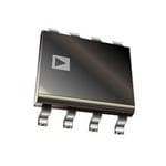
| 产品图片 |
|
| rohs | 符合RoHS无铅 / 符合限制有害物质指令(RoHS)规范要求 |
| 产品系列 | 接口 IC,数字隔离器,Analog Devices ADUM3221BRZiCoupler® |
| 数据手册 | |
| 产品型号 | ADUM3221BRZ |
| PulseWidthDistortion(Max) | - |
| 上升/下降时间(典型值) | 20ns, 20ns |
| 不同If时的传播延迟高-低 | 60ns |
| 产品种类 | |
| 传播延迟tpLH/tpHL(最大值) | 60ns, 60ns |
| 传播延迟时间 | 60 ns |
| 供应商器件封装 | 8-SOIC N |
| 共模瞬态抗扰度(最小值) | 25kV/µs |
| 包装 | 管件 |
| 商标 | Analog Devices |
| 安装类型 | 表面贴装 |
| 安装风格 | SMD/SMT |
| 封装 | Tube |
| 封装/外壳 | 8-SOIC(0.154",3.90mm 宽) |
| 封装/箱体 | SOIC-8 |
| 工作温度 | -40°C ~ 125°C |
| 工厂包装数量 | 98 |
| 技术 | 磁耦合 |
| 数据速率 | 1MHz |
| 最大工作温度 | + 125 C |
| 最大数据速率 | 1.2 Mb/s |
| 最小工作温度 | - 40 C |
| 标准包装 | 98 |
| 电压-正向(Vf)(典型值) | - |
| 电压-电源 | 3 V ~ 5.5 V,4.5 V ~ 18 V |
| 电压-隔离 | 2500Vrms |
| 电流-DC正向(If) | - |
| 电流-峰值输出 | 4A |
| 电流-输出/通道 | - |
| 电流-输出高,低 | - |
| 电源电压-最大 | 5 V |
| 电源电压-最小 | 3.3 V |
| 电源电流 | 700 uA, 1.2 mA |
| 类型 | General Purpose |
| 系列 | ADUM3221 |
| 绝缘电压 | 2.5 kVrms |
| 脉宽失真(最大) | - |
| 视频文件 | http://www.digikey.cn/classic/video.aspx?PlayerID=1364138032001&width=640&height=505&videoID=2219593469001http://www.digikey.cn/classic/video.aspx?PlayerID=1364138032001&width=640&height=505&videoID=2219593470001http://www.digikey.cn/classic/video.aspx?PlayerID=1364138032001&width=640&height=505&videoID=2219614223001 |
| 认可 | CSA, UR, VDE |
| 输入-输入侧1/输入侧2 | 2/0 |
| 输入类型 | - |
| 输出类型 | 栅极驱动器 |
| 通道数 | 2 |
| 通道数量 | 2 Channel |


.jpg)


- 商务部:美国ITC正式对集成电路等产品启动337调查
- 曝三星4nm工艺存在良率问题 高通将骁龙8 Gen1或转产台积电
- 太阳诱电将投资9.5亿元在常州建新厂生产MLCC 预计2023年完工
- 英特尔发布欧洲新工厂建设计划 深化IDM 2.0 战略
- 台积电先进制程称霸业界 有大客户加持明年业绩稳了
- 达到5530亿美元!SIA预计今年全球半导体销售额将创下新高
- 英特尔拟将自动驾驶子公司Mobileye上市 估值或超500亿美元
- 三星加码芯片和SET,合并消费电子和移动部门,撤换高东真等 CEO
- 三星电子宣布重大人事变动 还合并消费电子和移动部门
- 海关总署:前11个月进口集成电路产品价值2.52万亿元 增长14.8%


PDF Datasheet 数据手册内容提取
Isolated, 4 A Dual-Channel Gate Driver Data Sheet ADuM3220/ADuM3221 FEATURES GENERAL DESCRIPTION 4 A peak output current The ADuM3220/ADuM32211 are isolated, 4 A dual-channel gate Precise timing characteristics drivers based on the Analog Devices, Inc., iCoupler® technology. 60 ns maximum isolator and driver propagation delay Combining high speed CMOS and monolithic transformer technol- 5 ns maximum channel-to-channel matching ogy, these isolation components provide outstanding performance High junction temperature operation: 125°C characteristics superior to the alternatives, such as the combination 3.3 V to 5 V input logic of pulse transformers and gate drivers. 4.5 V to 18 V output drive The ADuM3220/ADuM3221 provide digital isolation in two UVLO at 2.5 V V DD1 independent isolation channels. They have a maximum propagation ADuM3220A/ADuM3221A UVLO at 4.1 V V DD2 delay of 60 ns and 5 ns channel-to-channel matching. In comparison ADuM3220B/ADuM3221B UVLO at 7.0 V V DD2 to gate drivers that employ high voltage level translation method- Thermal shutdown protection at >150°C ologies, the ADuM3220/ADuM3221 offer the benefit of true, Output shoot-through logic protection on the ADuM3220 galvanic isolation between the input and each output, enabling Default low output voltage translation across the isolation barrier. The ADuM3220 High frequency operation: dc to 1 MHz has shoot-through protection logic, which prevents both outputs CMOS input logic levels from being on at the same time, whereas the ADuM3221 allows High common-mode transient immunity: >25 kV/μs both outputs to be on at the same time. Both parts offer a default Enhanced system-level ESD performance per IEC 61000-4-x output low characteristic as required for gate drive applications. Safety and regulatory approvals UL recognition The ADuM3220/ADuM3221 operate with an input supply voltage 2500 V rms for 1 minute per UL 1577 ranging from 3.0 V to 5.5 V, providing compatibility with lower CSA Component Acceptance Notice #5A voltage systems. The outputs of the ADuM3220A/ADuM3221A VDE certificate of conformity can be operated at supply voltages from 4.5 V to 18 V. The outputs DIN V VDE V 0884-10 (VDE V 0884-10):2006-12 of the ADuM3220B/ADuM3221B can be operated at supply V = 560 V peak voltages from 7.6 V to 18 V. IORM Small footprint and low profile The junction temperature of the ADuM3220/ADuM3221 is Narrow body, RoHS-compliant, 8-lead SOIC specified from −40°C to +125°C. 5 mm × 6 mm × 1.6 mm Qualified for automotive applications APPLICATIONS Isolated synchronous dc-to-dc converters MOSFET/IGBT gate drivers FUNCTIONAL BLOCK DIAGRAMS ADuM3220 ADuM3221 VDD1 1 8 VDD2 VDD1 1 8 VDD2 DECODE DECODE VIA 2 ENCODE LAENVDEL 7 VOA VIA 2 ENCODE LAENVDEL 7 VOA SHIFT SHIFT DECODE DECODE VIB 3 ENCODE LAENVDEL 6 VOB VIB 3 ENCODE LAENVDEL 6 VOB SHIFT SHIFT GND1 4 5 GND2 08994-001 GND1 4 5 GND2 08994-102 Figure 1. Figure 2. 1 Protected by U.S. Patents 5,952,849; 6,873,065; 7,075,239. Rev. C Document Feedback Information furnished by Analog Devices is believed to be accurate and reliable. However, no responsibility is assumed by Analog Devices for its use, nor for any infringements of patents or other One Technology Way, P.O. Box 9106, Norwood, MA 02062-9106, U.S.A. rights of third parties that may result from its use. Specifications subject to change without notice. No license is granted by implication or otherwise under any patent or patent rights of Analog Devices. Tel: 781.329.4700 ©2010–2012 Analog Devices, Inc. All rights reserved. Trademarks and registered trademarks are the property of their respective owners. Technical Support www.analog.com
ADuM3220/ADuM3221 Data Sheet TABLE OF CONTENTS Features .............................................................................................. 1 Pin Configuration and Function Descriptions ..............................8 Applications ....................................................................................... 1 Typical Performance Characteristics ..............................................9 General Description ......................................................................... 1 Applications Information .............................................................. 12 Functional Block Diagrams ............................................................. 1 PC Board Layout ........................................................................ 12 Revision History ............................................................................... 2 Propagation Delay-Related Parameters ................................... 12 Specifications ..................................................................................... 3 Thermal Limitations and Switch Load Characteristics ......... 12 Electrical Characteristics—5 V Operation................................ 3 Output Load Characteristics ..................................................... 12 Electrical Characteristics—3.3 V Operation ............................ 4 DC Correctness and Magnetic Field Immunity.......................... 13 Package Characteristics ............................................................... 5 Power Consumption .................................................................. 14 Regulatory Information ............................................................... 5 Insulation Lifetime ..................................................................... 14 Insulation and Safety-Related Specifications ............................ 5 Outline Dimensions ....................................................................... 15 DIN V VDE V 0884-10 (VDE V 0884-10) Insulation Ordering Guide .......................................................................... 15 Characteristics .............................................................................. 6 Automotive Products ................................................................. 15 Recommended Operating Conditions ...................................... 6 Absolute Maximum Ratings ............................................................ 7 ESD Caution .................................................................................. 7 REVISION HISTORY 3/11—Rev. A to Rev. B 10/12—Rev. B to Rev. C Added ADuM3220BRZ and ADuM3221BRZ models.... Universal Changes to Features Section and General Description Section .... 1 Changes to Features Section and General Description Section .. 1 Created Hyperlink for Safety and Regulatory Approvals Changes to Table 1 ............................................................................. 3 Entry in Features Section ................................................................. 1 Changes to Table 2 ............................................................................. 4 Added Output Pulsed Source Resistance Parameter Added Figure 17 and Figure 18; Renumbered Sequentially ..... 11 and Output Pulsed Sink Resistance Parameter to Table 1 .......... 3 Changes to Ordering Guide .......................................................... 14 Added Output Pulsed Source Resistance Parameter and Output Pulsed Sink Resistance Parameter to Table 2 .......... 4 1/11—Rev. 0 to Rev. A Added IC Junction-to-Ambient Thermal Resistance Added ADuM3221 ............................................................. Universal Parameter to Table 3 ......................................................................... 5 Changes to Features Section and General Description Section .. 1 Changes to Introductory Sentence of Regulatory Added Figure 2; Renumbered Sequentially ................................... 1 Information Section ......................................................................... 5 Changes to Endnote 3, Endnote 4, and Endnote 5, Table 1 ......... 3 Changed Supply Voltage Ranges Parameter in Table 8 ............... 7 Changes to Endnote 3, Endnote 4, and Endnote 5, Table 2 ......... 4 Changes to Table 9 ............................................................................ 7 Changes to Table 8 ............................................................................. 7 Changes to Table 11 and Table 12 .................................................. 8 Changes to Figure 4, Table 10, and Table 11 .................................. 8 Added Figure 17 and Figure 18; Renumbered Sequentially ..... 11 Added Table 12; Renumbered Sequentially ................................... 8 Moved Figure 21 ............................................................................. 12 Added Figure 8................................................................................... 9 Changes to Power Consumption Section and Insulation Change to Figure 19 and DC Correctness and Magnetic Field Lifetime Section .............................................................................. 14 Immunity Section ........................................................................... 12 Changes to Ordering Guide .......................................................... 15 Changes to Ordering Guide .......................................................... 14 Added Automotive Products Section........................................... 15 4/10—Revision 0: Initial Version Rev. C | Page 2 of 16
Data Sheet ADuM3220/ADuM3221 SPECIFICATIONS ELECTRICAL CHARACTERISTICS—5 V OPERATION All voltages are relative to their respective ground. 4.5 V ≤ V ≤ 5.5 V, 4.5 V ≤ V ≤ 18 V, unless stated otherwise. All minimum/ DD1 DD2 maximum specifications apply over T = −40°C to +125°C. All typical specifications are at T = 25°C, V = 5 V, V = 10 V. Switching J J DD1 DD2 specifications are tested with CMOS signal levels. Table 1. Parameter Symbol Min Typ Max Unit Test Conditions/Comments DC SPECIFICATIONS Input Supply Current, Two Channels, Quiescent I 1.2 1.5 mA DDI(Q) Output Supply Current, Two Channels, Quiescent I 4.7 10 mA DDO(Q) Total Supply Current, Two Channels1 DC to 1 MHz V Supply Current I 1.4 1.7 mA DC to 1 MHz logic signal frequency DD1 DD1(Q) V Supply Current I 11 17 mA DC to 1 MHz logic signal frequency DD2 DD2(Q) Input Currents I , I −10 +0.01 +10 µA 0 V ≤ V , V ≤ V IA IB IA IB DD1 Logic High Input Threshold V 0.7 × V V IH DD1 Logic Low Input Threshold V 0.3 × V V IL DD1 Logic High Output Voltages V , V V − 0.1 V V I = −20 mA, V = V OAH OBH DD2 DD2 Ox Ix IxH Logic Low Output Voltages V , V 0.0 0.15 V I = +20 mA, V = V OAL OBL Ox Ix IxL Undervoltage Lockout, V Supply DD2 ADuM3220A/ADuM3221A Positive-Going Threshold V 4.1 4.4 V DD2UV+ Negative-Going Threshold V 3.2 3.7 V DD2UV− Hysteresis V 0.4 V DD2UVH ADuM3220B/ADuM3221B Positive-Going Threshold V 7.0 7.5 V DD2UV+ Negative-Going Threshold V 6.0 6.5 V DD2UV− Hysteresis V 0.5 V DD2UVH Output Short-Circuit Pulsed Current2 I , I 2.0 4.0 A V = 10 V OA(SC) OB(SC) DD2 Output Pulsed Source Resistance R , R 0.3 1.3 3.0 Ω V = 10 V OA OB DD2 Output Pulsed Sink Resistance R , R 0.3 0.9 3.0 Ω V = 10 V OA OB DD2 SWITCHING SPECIFICATIONS Pulse Width3 PW 50 ns C = 2 nF, V = 10 V L DD2 Data Rate4 1 MHz C = 2 nF, V = 10 V L DD2 Propagation Delay5 t , t 35 45 60 ns C = 2 nF, V = 10 V; see Figure 20 DLH DHL L DD2 t , t 36 50 68 ns C = 2 nF, V = 4.5 V; see Figure 20 DLH DHL L DD2 Propagation Delay Skew6 t 12 ns C = 2 nF, V = 10 V; see Figure 20 PSK L DD2 Channel-to-Channel Matching7 t 1 5 ns C = 2 nF, V = 10 V; see Figure 20 PSKCD L DD2 t 1 7 ns C = 2 nF, V = 4.5 V; see Figure 20 PSKCD L DD2 Output Rise/Fall Time (10% to 90%) t/t 14 20 25 ns C = 2 nF, V = 10 V; see Figure 20 R F L DD2 t/t 14 22 28 ns C = 2 nF, V = 4.5 V; see Figure 20 R F L DD2 Dynamic Input Supply Current per Channel I 0.05 mA/Mbps V = 10 V DDI(D) DD2 Dynamic Output Supply Current per Channel I 1.5 mA/Mbps V = 10 V DDO(D) DD2 Refresh Rate f 1.2 Mbps r 1 The supply current values for both channels are combined when running at identical data rates. Output supply current values are specified with no output load present. The supply current associated with an individual channel operating at a given data rate can be calculated as described in the Power Consumption section. See Figure 9 and Figure 10 for total V and V supply currents as a function of frequency. DD1 DD2 2 Short-circuit duration less than 1 µs. Average power must conform to the limit shown in the Absolute Maximum Ratings section. 3 The minimum pulse width is the shortest pulse width at which the specified timing parameter is guaranteed. 4 The maximum data rate is the fastest data rate at which the specified timing parameter is guaranteed. 5 t propagation delay is measured from the time of the input rising logic high threshold, V , to the output rising 10% threshold of the V signal. t propagation DLH IH Ox DHL delay is measured from the input falling logic low threshold, V , to the output falling 90% threshold of the V signal. See Figure 20 for waveforms of propagation IL Ox delay parameters. 6 t is the magnitude of the worst-case difference in t and/or t that is measured between units at the same operating temperature, supply voltages, and output PSK DLH DHL load within the recommended operating conditions. See Figure 20 for waveforms of propagation delay parameters. 7 Channel-to-channel matching is the absolute value of the difference in propagation delays between any two channels with inputs on the same side of the isolation barrier. Rev. C | Page 3 of 16
ADuM3220/ADuM3221 Data Sheet ELECTRICAL CHARACTERISTICS—3.3 V OPERATION All voltages are relative to their respective ground. 3.0 V ≤ V ≤ 3.6 V, 4.5 V ≤ V ≤ 18 V, unless stated otherwise. All minimum/ DD1 DD2 maximum specifications apply over T = −40°C to +125°C. All typical specifications are at T = 25°C, V = 3.3 V, V = 10 V. Switching J J DD1 DD2 specifications are tested with CMOS signal levels. Table 2. Parameter Symbol Min Typ Max Unit Test Conditions/Comments DC SPECIFICATIONS Input Supply Current, Two Channels, Quiescent I 0.7 1.0 mA DDI(Q) Output Supply Current, Two Channels, I 4.7 10 mA DDO(Q) Quiescent Total Supply Current, Two Channels1 DC to 1 MHz V Supply Current I 0.8 1.0 mA DC to 1 MHz logic signal frequency DD1 DD1(Q) V Supply Current I 11 17 mA DC to 1 MHz logic signal frequency DD2 DD2(Q) Input Currents I , I −10 +0.01 +10 µA 0 V ≤ V , V ≤ V IA IB IA IB DD1 Logic High Input Threshold V 0.7 × V V IH DD1 Logic Low Input Threshold V 0.3 × V V IL DD1 Logic High Output Voltages V , V V − 0.1 V V I = −20 mA, V = V OAH OBH DD2 DD2 Ox Ix IxH Logic Low Output Voltages V , V 0.0 0.15 V I = +20 mA, V = V OAL OBL Ox Ix IxL Undervoltage Lockout, V Supply DD2 ADuM3220A/ADuM3221A Positive-Going Threshold V 4.1 4.4 V DD2UV+ Negative-Going Threshold V 3.2 3.7 V DD2UV− Hysteresis V 0.4 V DD2UVH ADuM3220B/ADuM3221B Positive-Going Threshold V 7.0 7.5 V DD2UV+ Negative-Going Threshold V 6.0 6.5 V DD2UV− Hysteresis V 0.5 V DD2UVH Output Short-Circuit Pulsed Current2 I , I 2.0 4.0 A V = 10 V OA(SC) OB(SC) DD2 Output Pulsed Source Resistance R , R 0.3 1.3 3.0 Ω V = 10 V OA OB DD2 Output Pulsed Sink Resistance R , R 0.3 0.9 3.0 Ω V = 10 V OA OB DD2 SWITCHING SPECIFICATIONS Pulse Width3 PW 50 ns C = 2 nF, V = 10 V L DD2 Data Rate4 1 MHz C = 2 nF, V = 10 V L DD2 Propagation Delay5 t , t 36 48 62 ns C = 2 nF, V = 10 V; see Figure 20 DLH DHL L DD2 t , t 37 53 72 ns C = 2 nF, V = 4.5 V; see Figure 20 DLH DHL L DD2 Propagation Delay Skew6 t 12 ns C = 2 nF, V = 10 V; see Figure 20 PSK L DD2 Channel-to-Channel Matching7 t 1 5 ns C = 2 nF, V = 10 V; see Figure 20 PSKCD L DD2 t 1 7 ns C = 2 nF, V = 4.5 V; see Figure 20 PSKCD L DD2 Output Rise/Fall Time (10% to 90%) t/t 14 20 25 ns C = 2 nF, V = 10 V; see Figure 20 R F L DD2 t/t 14 22 28 ns C = 2 nF, V = 4.5 V; see Figure 20 R F L DD2 Dynamic Input Supply Current per Channel I 0.025 mA/Mbps V = 10 V DDI(D) DD2 Dynamic Output Supply Current per Channel I 1.5 mA/Mbps V = 10 V DDO(D) DD2 Refresh Rate f 1.1 Mbps r 1 The supply current values for both channels are combined when running at identical data rates. Output supply current values are specified with no output load present. The supply current associated with an individual channel operating at a given data rate can be calculated as described in the Power Consumption section. See Figure 9 and Figure 10 for total V and V supply currents as a function of frequency. DD1 DD2 2 Short-circuit duration less than 1 µs. Average power must conform to the limit shown in the Absolute Maximum Ratings section. 3 The minimum pulse width is the shortest pulse width at which the specified timing parameter is guaranteed. 4 The maximum data rate is the fastest data rate at which the specified timing parameter is guaranteed. 5 t propagation delay is measured from the time of the input rising logic high threshold, V , to the output rising 10% threshold of the V signal. t propagation DLH IH Ox DHL delay is measured from the input falling logic low threshold, V , to the output falling 90% threshold of the V signal. See Figure 20 for waveforms of propagation IL Ox delay parameters. 6 t is the magnitude of the worst-case difference in t and/or t that is measured between units at the same operating temperature, supply voltages, and output PSK DLH DHL load within the recommended operating conditions. See Figure 20 for waveforms of propagation delay parameters. 7 Channel-to-channel matching is the absolute value of the difference in propagation delays between any two channels with inputs on the same side of the isolation barrier. Rev. C | Page 4 of 16
Data Sheet ADuM3220/ADuM3221 PACKAGE CHARACTERISTICS Table 3. Parameter Symbol Min Typ Max Unit Test Conditions/Comments Resistance (Input-to-Output)1 R 1012 Ω I-O Capacitance (Input-to-Output)1 C 1.0 pF f = 1 MHz I-O Input Capacitance C 4.0 pF I IC Junction-to-Case Thermal Resistance, Side 1 θ 46 °C/W Thermocouple located at center JCI of package underside IC Junction-to-Case Thermal Resistance, Side 2 θ 41 °C/W Thermocouple located at center JCO of package underside IC Junction-to-Ambient Thermal Resistance θ 85 °C/W Thermocouple located at center JA of package underside 1 The device is considered a 2-terminal device; Pin 1 through Pin 4 are shorted together, and Pin 5 through Pin 8 are shorted together. REGULATORY INFORMATION The ADuM3220/ADuM3221 are approved by the organizations listed in Table 4. Table 4. UL CSA VDE Recognized Under UL 1577 Approved under CSA Component Acceptance Notice #5A Certified according to DIN V VDE V 0884-10 Component Recognition (VDE V 0884-10):2006-122 Program1 Single/Basic 2500 V rms Basic insulation per CSA 60950-1-03 and IEC 60950-1, Reinforced insulation, 560 V peak Isolation Voltage 400 V rms (566 V peak) maximum working voltage Functional insulation per CSA 60950-1-03 and IEC 60950-1, 800 V rms (1131 V peak) maximum working voltage File E214100 File 205078 File 2471900-4880-0001 1 In accordance with UL 1577, each ADuM3220/ADuM3221 is proof tested by applying an insulation test voltage ≥ 3000 V rms for 1 second (current leakage detection limit = 5 µA). 2 In accordance with DIN V VDE V 0884-10, each ADuM3220/ADuM3221 is proof tested by applying an insulation test voltage ≥ 1050 V peak for 1 second (partial discharge detection limit = 5 pC). An asterisk (*) marking branded on the component designates DIN V VDE V 0884-10 approval. INSULATION AND SAFETY-RELATED SPECIFICATIONS Table 5. Parameter Symbol Value Unit Test Conditions/Comments Rated Dielectric Insulation Voltage 2500 V rms 1 minute duration Minimum External Air Gap (Clearance) L(I01) 4.90 min mm Measured from input terminals to output terminals, shortest distance through air Minimum External Tracking (Creepage) L(I02) 4.01 min mm Measured from input terminals to output terminals, shortest distance path along body Minimum Internal Gap (Internal Clearance) 0.017 min mm Insulation distance through insulation Tracking Resistance (Comparative Tracking Index) CTI >175 V DIN IEC 112/VDE 0303 Part 1 Isolation Group IIIa Material Group (DIN VDE 0110, 1/89, Table 1) Rev. C | Page 5 of 16
ADuM3220/ADuM3221 Data Sheet DIN V VDE V 0884-10 (VDE V 0884-10) INSULATION CHARACTERISTICS These isolators are suitable for reinforced isolation only within the safety limit data. Maintenance of the safety data is ensured by protective circuits. The asterisk (*) marking on the package denotes DIN V VDE V 0884-10 approval for a 560 V peak working voltage. Table 6. Description Test Conditions/Comments Symbol Characteristic Unit Installation Classification per DIN VDE 0110 For Rated Mains Voltage ≤ 150 V rms I to IV For Rated Mains Voltage ≤ 300 V rms I to III For Rated Mains Voltage ≤ 400 V rms I to II Climatic Classification 40/105/21 Pollution Degree per DIN VDE 0110, Table 1 2 Maximum Working Insulation Voltage V 560 V peak IORM Input-to-Output Test Voltage, Method B1 V × 1.875 = V , 100% production test, t = 1 sec, V 1050 V peak IORM PR m PR partial discharge < 5 pC Input-to-Output Test Voltage, Method A V × 1.6 = V , t = 60 sec, partial discharge < 5 pC V IORM PR m PR After Environmental Tests Subgroup 1 896 V peak After Input and/or Safety Tests Subgroup 2 V × 1.2 = V , t = 60 sec, partial discharge < 5 pC V 672 V peak IORM PR m PR and Subgroup 3 Highest Allowable Overvoltage Transient overvoltage, t = 10 sec V 4000 V peak TR TR Safety-Limiting Values Maximum value allowed in the event of a failure (see Figure 3) Case Temperature T 150 °C S Side 1 Current I 160 mA S1 Side 2 Current I 47 mA S2 Insulation Resistance at T V = 500 V R >109 Ω S IO S 200 RECOMMENDED OPERATING CONDITIONS 180 Table 7. A) 160 m Parameter Symbol Min Max Unit T ( 140 EN SIDE 1 Operating Junction TJ −40 +125 °C RR 120 Temperature U G C 100 Supply Voltages1 VDD1 3.0 5.5 V MITIN 80 VDD2 4.5 18 V TY-LI 60 SIDE 2 VCDoDm1 Rmisoen T-Mimoed e Transient tVDD1 − 25 +1 25 kVV/µ/µs s E AF 40 Immunity, Input to Output S 20 Input Signal Rise and Fall 1 ms Times 00 50CASE TEMP1E0R0ATURE (°C)150 200 08994-002 1 All voltages are relative to their respective ground. See the DC Correctness Figure 3. Thermal Derating Curve; Dependence of Safety-Limiting Values and Magnetic Field Immunity section for information about immunity to on Case Temperature, per DIN V VDE V 0884-10 (Safety-Limiting Current external magnetic fields. Is Defined as the Average Current at Maximum V ) DD Rev. C | Page 6 of 16
Data Sheet ADuM3220/ADuM3221 ABSOLUTE MAXIMUM RATINGS Ambient temperature = 25°C, unless otherwise noted. Table 8. Table 9. Maximum Continuous Working Voltage1 Parameter Rating Parameter Max Unit Constraint Storage Temperature (T ) −55°C to +150°C AC Bipolar Voltage2 565 V peak 50-year minimum lifetime ST Operating Temperature (T) −40°C to +150°C AC Unipolar Voltage3 1131 V peak 50-year minimum lifetime J Supply Voltage Ranges1 DC Voltage4 1131 V peak 50-year minimum lifetime V −0.5 V to +7.0 V 1 Refers to the continuous voltage magnitude imposed across the isolation DD1 V −0.5 V to +20 V barrier. See the Insulation Lifetime section for more information. DD2 2 See Figure 24. Input Voltage Range (VIA, VIB)1, 2 −0.5 V to VDDI + 0.5 V 3 See Figure 25. Output Voltage Range (V , V )1, 2 −0.5 V to V + 0.5 V 4 See Figure 26. OA OB DDO Average Output Current per Pin (I )3 −23 mA to +23 mA O Common-Mode Transients, −100 kV/µs to +100 kV/µs ESD CAUTION (CM , CM)4 H L 1 All voltages are relative to their respective ground. 2 V and V refer to the supply voltages on the input and output sides of DDI DDO a given channel, respectively. 3 See Figure 3 for information about maximum allowable current for various temperatures. 4 Refers to common-mode transients across the insulation barrier. Common- mode transients exceeding the Absolute Maximum Rating can cause latch-up or permanent damage. Stresses above those listed under Absolute Maximum Ratings may cause permanent damage to the device. This is a stress rating only; functional operation of the device at these or any other conditions above those indicated in the operational section of this specification is not implied. Exposure to absolute maximum rating conditions for extended periods may affect device reliability. Rev. C | Page 7 of 16
ADuM3220/ADuM3221 Data Sheet PIN CONFIGURATION AND FUNCTION DESCRIPTIONS VDD1 1 ADuM3220/ 8 VDD2 VIA 2 ADuM3221 7 VOA GNVDIB1 34 (NToOt Pto V SIEcaWle) 56 VGONBD2 08994-003 Figure 4. Pin Configuration Table 10. Pin Function Descriptions Pin No. Mnemonic Description 1 V Supply Voltage for Isolator Side 1, 3.0 V to 5.5 V. DD1 2 V Logic Input A. IA 3 V Logic Input B. IB 4 GND Ground 1. Ground reference for Isolator Side 1. 1 5 GND Ground 2. Ground reference for Isolator Side 2. 2 6 V Logic Output B. OB 7 V Logic Output A. OA 8 V Supply Voltage for Isolator Side 2, 4.5 V to 18 V. DD2 Table 11. Truth Table, ADuM3220 (Positive Logic)1 V Input V Input V State V State V Output V Output Notes IA IB DD1 DD2 OA OB L L Powered Powered L L L H Powered Powered L H H L Powered Powered H L H H Powered Powered L L X X Unpowered Powered L L Outputs return to the input state within 1 µs of V power restoration. DD1 X X Powered Unpowered L L Outputs return to the input state within 1 µs of V power restoration. DD2 1 X = don’t care, L = low, H = high. Table 12. Truth Table, ADuM3221 (Positive Logic)1 V Input V Input V State V State V Output V Output Notes IA IB DD1 DD2 OA OB L L Powered Powered L L L H Powered Powered L H H L Powered Powered H L H H Powered Powered H H X X Unpowered Powered L L Outputs return to the input state within 1 µs of V power restoration. DD1 X X Powered Unpowered L L Outputs return to the input state within 1 µs of V power restoration. DD2 1 X = don’t care, L = low, H = high. Rev. C | Page 8 of 16
Data Sheet ADuM3220/ADuM3221 TYPICAL PERFORMANCE CHARACTERISTICS 300 VDD2 = 15V VDD2 = 10V 250 VDD2 = 8V VDD2 = 5V CH2 = VO (2V/DIV) nC) 200 E ( G R A 150 H C E T 2 GA 100 CH1 = VI (5V/DIV) 50 1 CH1 5V Ω CH2 2VΩ MT 4 02n2.s2% 21.05kG PSOPISNTS CH2 7.2V 08994-004 00 200 SWITCH4I0N0G FREQUE60N0CY (kHz) 800 1000 08994-107 Figure 5. Output Waveform for 2 nF Load with 10 V Output Supply Figure 8. Typical Maximum Load vs. Switching Frequency (R = 1 Ω) GATE 2.0 CH2 = VO (2V/DIV) 1.5 A) m NT ( VDD1 = 5V E R 1.0 R U C D1 VDD1 = 3.3V 2 ID CH1 = VI (5V/DIV) 0.5 1 CH1 5V Ω CH2 2VΩ MT 4 02n1.s4% 21.05kG PSOPISNTS CH2 7.2V 08994-005 00 0.25 FREQUE0N.5C0Y (MHz) 0.75 1.00 08994-015 Figure 6. Output Waveform for 1 nF Load with 10 V Output Supply Figure 9. Typical I Supply Current vs. Frequency DD1 80 CH2 = VO (2V/DIV) 70 VDD2 = 15V 60 T (mA) 50 VDD2 = 10V N E R 40 R U C 2 I DD2 30 VDD2 = 5V CH1 = VI (5V/DIV) 20 1 10 CH1 5V Ω CH2 2VΩ MT 4 02n2.s1% 21.05kG PSOPISNTS CH2 7.2V 08994-006 00 0.25 FREQUE0N.5C0Y (MHz) 0.75 1.00 08994-016 Figure 7. Output Waveform for 1 nF Load with 5 Ω Series Resistance Figure 10. Typical I Supply Current vs. Frequency with 2 nF Load DD2 and 10 V Output Supply Rev. C | Page 9 of 16
ADuM3220/ADuM3221 Data Sheet 60 30 50 25 s) n ON DELAY ( 3400 L TIME (ns) 1250 FALL TIME ATI FAL OPAG 20 RISE/ 10 RISE TIME R P 10 5 0–40 –20 0 JUN2C0TION 4T0EMPE6R0ATUR8E0 (°C)100 120 140 08994-017 05 7 OU9TPUT SU1P1PLY VOL1T3AGE (V)15 17 08994-020 Figure 11. Typical Propagation Delay vs. Temperature Figure 14. Typical Rise/Fall Time Variation vs. Output Supply Voltage 60 5 L E N N A 50 H s) tDHL O-C 4 AGATION DELAY (n 3400 tDLH DELAY CHANNEL-TMATCHING (ns) 23 PROP 20 TION PD MATCHtDLH 10 AGA 1 OP PD MATCHtDHL R P 0 0 3.0 3.5 INPUT 4S.U0PPLY VOL4T.A5GE (V) 5.0 5.5 08994-018 5 7 OU9TPUT SUP11PLY VOL1T3AGE (V)15 17 08994-021 Figure 12. Typical Propagation Delay vs. Input Supply Voltage, V = 10 V Figure 15. Typical Propagation Delay Channel-to-Channel Matching DD2 vs. Output Supply Voltage 60 5 L tDHL NE N OPAGATION DELAY (ns) 23450000 tDLH N DELAY CHANNEL-TO-CHAMATCHING (ns) 234 R O P 10 AGATI 1 PD MATCHtDLH P O R PD MATCHtDHL P 05 7 OU9TPUT SU1P1PLY VOL1T3AGE (V)15 17 08994-019 0–40 –20 0 JUNC20TION 4T0EMPE6R0ATUR8E0 (°C)100 120 140 08994-022 Figure 13. Typical Propagation Delay vs. Output Supply Voltage, V = 5 V Figure 16. Typical Propagation Delay Channel-to-Channel Matching DD1 vs. Temperature, V = 10 V DD2 Rev. C | Page 10 of 16
Data Sheet ADuM3220/ADuM3221 1.6 8 1.4 A) 7 VOUTSOURCERESISTANCE T( N 1.2 RE 6 SOURCE IOUT R U 1.0 C 5 Ω) VOUTSINKRESISTANCE NK (UT 0.8 E/SI 4 O C R R U 0.6 O 3 S 0.4 MUM 2 SINK IOUT XI A 0.2 M 1 04 6 O8UTPUT S1U0PPLY V1O2LTAGE 1(V4) 16 18 08994-116 04 6 O8UTPUT S1U0PPLY V1O2LTAGE 1(V4) 16 18 08994-117 Figure 17. Typical Output Source Resistance vs. Output Supply Voltage Figure 18. Typical Maximum Source/Sink Current vs. Output Supply Voltage Rev. C | Page 11 of 16
ADuM3220/ADuM3221 Data Sheet APPLICATIONS INFORMATION PC BOARD LAYOUT THERMAL LIMITATIONS AND SWITCH LOAD CHARACTERISTICS The ADuM3220/ADuM3221 digital isolators require no exter- nal interface circuitry for the logic interfaces. Power supply For isolated gate drivers, the necessary separation between the bypassing is required at the input and output supply pins, as input and output circuits prevents the use of a single thermal pad shown in Figure 19. Use a small ceramic capacitor with a value beneath the part; therefore, heat is dissipated mainly through from 0.01 µF to 0.1 µF to provide a good high frequency bypass. the package pins. On the output power supply pin, V , it is recommended that a DD2 Package thermal dissipation limits the performance of switching 10 µF capacitor also be added to provide the charge required to frequency vs. output load, as illustrated in Figure 8, which shows drive the gate capacitance at the ADuM3220/ADuM3221 outputs. the maximum load capacitance that can be driven with a 1 Ω series On the output supply pin, the use of vias with the bypass capacitor gate resistor for different values of output voltage. For example, should be avoided, or multiple vias should be used to reduce the this curve shows that a typical ADuM3220/ADuM3221 can drive inductance in the bypassing. The total lead length between both a large MOSFET with 120 nC gate charge at 8 V output (which is ends of the smaller capacitor and the input or output power equivalent to a 15 nF load) up to a frequency of about 300 kHz. supply pin should not exceed 20 mm. OUTPUT LOAD CHARACTERISTICS VDD1 VDD2 VIA VOA The ADuM3220/ADuM3221 output signals depend on the GND1 VIB VOB GND2 08994-023 cMhOarSaFctEeTri. sTtihcse odfr itvheer oouuttppuutt lroeasdp,o wnhseic tho iasn t yNp-iccahlalyn nanel NM-OchSaFnEnTe l Figure 19. Recommended PCB Layout load can be modeled with a switch output resistance (R ), an SW PROPAGATION DELAY-RELATED PARAMETERS inductance due to the printed circuit board trace (L ), a series TRACE gate resistor (R ), and a gate-to-source capacitance (C ), as Propagation delay is a parameter that describes the time it takes a GATE GS shown in Figure 21. logic signal to propagate through a component. The propagation delay to a logic low output can differ from the propagation delay ftaaaonsl dlatihn tleohg getpi imorco uhept ipabgugehatt tworiiouesntienpn dgu et t1h.l a0eTy% ,hi nt etp hAure,tD sirshui sdoMilend3fgi 2n( hs2eei0dge/ haAF silD gotuhgueriMce t i2t3mh02r)e2e. 1sbLh esikotpweledwec,ei ifVsnye I ,tHt htD,h eLHe VIA AADDuuMM33222201/ VOA RSWLTRACERGATE CGSVO 08994-118 DHL Figure 21. RLC Model of the Gate of an N-Channel MOSFET input falling logic low threshold, V , and the output falling 90% IL threshold. The rise and fall times are dependent on the loading RSW is the switch resistance of the internal ADuM3220/ADuM3221 conditions and are not included in the propagation delay, as is driver output, which is about 1.5 Ω. RGATE is the intrinsic gate the industry standard for gate drivers. resistance of the MOSFET and any external series resistance. A MOSFET that requires a 4 A gate driver has a typical intrinsic gate resistance of about 1 Ω and a gate-to-source capacitance, 90% C , from 2 nF to 10 nF. L is the inductance of the printed GS TRACE OUTPUT circuit board trace, typically a value of 5 nH or less for a well- 10% designed layout with a very short and wide connection from the ADuM3220/ADuM3221 output to the gate of the MOSFET. VIH The following equation defines the Q factor of the RLC circuit, INPUT which indicates how the ADuM3220/ADuM3221 output responds VIL to a step change. For a well-damped output, Q is less than 1. tDLH tDHL Adding a series gate resistor dampens the output response. tR tF 08994-007 Q= (R +1R )× LTCRACE Figure 20. Propagation Delay Parameters SW GATE GS Channel-to-channel matching refers to the maximum amount In Figure 5 and Figure 6, the ADuM3220/ADuM3221 output that the propagation delay differs between channels within a waveforms for 10 V output are shown for a C of 2 nF and 1 nF, GS single ADuM3220/ADuM3221 component. respectively. Note the ringing of the output in Figure 6 with C GS of 1 nF and a calculated Q factor of 1.5, where less than 1 is Propagation delay skew refers to the maximum amount that desired for good damping. the propagation delay differs between multiple ADuM3220/ ADuM3221 components operating under the same conditions. Rev. C | Page 12 of 16
Data Sheet ADuM3220/ADuM3221 Output ringing can be reduced by adding a series gate resistor 100 to dampen the response. For applications that use a load of 1 nF X U L or less, it is recommended that a series gate resistor of about 5 Ω C F 10 be added. As shown in Figure 7, RGATE is 5 Ω, which yields a NETI rDceasClcp uColnOasteeRd iRn QE c CofamTcNtpoaErr SoisfSo a nAb owNuiDtth 0 M.F3i.Ag FuGirgeNu 6rE.e T 7I Cill FusIEtrLatDes I Ma dMamUpNedIT Y OWABLE MAGNSITY (kgauss)0.11 LE Positive and negative logic transitions at the isolator input cause ALD narrow (~1 ns) pulses to be sent to the decoder via the transformer. UM M 0.01 The decoder is bistable and is, therefore, either set or reset by the XI A M pulses, indicating input logic transitions. In the absence of logic ptrualnsseist iionndsi coaf tmivoe roef t thhaen c 1o rµrse actt tihnep uint psutat,t ea ipse sreiondt itco seent soufr ree fdrce sh 0.0011k 10kMAGNETI1C0 0FkIELD FREQ1MUENCY (Hz1)0M 100M 08994-009 correctness at the output. Figure 22. Maximum Allowable External Magnetic Flux Density If the decoder receives no internal pulses for more than about For example, at a magnetic field frequency of 1 MHz, the maxi- 3 µs, the input side is assumed to be unpowered or nonfunc- mum allowable magnetic field of 0.2 kgauss induces a voltage tional, in which case the isolator output is forced to a default of 0.25 V at the receiving coil. This is about 50% of the sensing low state by the watchdog timer circuit. In addition, the outputs threshold and does not cause a faulty output transition. Simi- are in a low default state while the power is rising before the larly, if such an event were to occur during a transmitted pulse UVLO threshold is crossed. (and had the worst-case polarity), the received pulse is reduced The ADuM3220/ADuM3221 are immune to external magnetic from >1.0 V to 0.75 V, still well above the 0.5 V sensing thresh- fields. The limitation on the ADuM3220/ADuM3221 magnetic old of the decoder. field immunity is set by the condition in which induced voltage The preceding magnetic flux density values correspond to in the transformer receiving coil is sufficiently large to either specific current magnitudes at given distances away from the falsely set or reset the decoder. The following analysis defines ADuM3220/ADuM3221 transformers. Figure 23 expresses the conditions under which this can occur. The 3 V operating these allowable current magnitudes as a function of frequency condition of the ADuM3220/ADuM3221 is examined because for selected distances. As shown, the ADuM3220/ADuM3221 it represents the most susceptible mode of operation. The pulses are immune and can be affected only by extremely large currents at the transformer output have an amplitude greater than 1.0 V. operated at a high frequency very close to the component. For The decoder has a sensing threshold at about 0.5 V, therefore the 1 MHz example, a 0.5 kA current must be placed 5 mm establishing a 0.5 V margin in which induced voltages can be away from the ADuM3220/ADuM3221 to affect the operation tolerated. The voltage induced across the receiving coil is given by of the component. V = (−dβ/dt) ∑ πr2; n = 1, 2, ... , N 1000 n where: A) DISTANCE = 1m k β is the magnetic flux density (gauss). T ( 100 N E r is the radius of the nth turn in the receiving coil (cm). R n R U N is the number of turns in the receiving coil. C E 10 L Given the geometry of the receiving coil in the ADuM3220/ AB DISTANCE = 100mm W ADuM3221 and an imposed requirement that the induced O L 1 L voltage be, at most, 50% of the 0.5 V margin at the decoder, A M DISTANCE = 5mm a maximum allowable magnetic field is calculated, as shown U M in Figure 22. AXI 0.1 M 0.01 1k 10MkAGNET1IC0 0FkIELD FRE1QMUENCY (H1z0)M 100M 08994-010 Figure 23. Maximum Allowable Current for Various Current-to-ADuM3220/ADuM3221 Spacings Rev. C | Page 13 of 16
ADuM3220/ADuM3221 Data Sheet POWER CONSUMPTION The values shown in Table 9 summarize the peak voltage for 50 years of service life. In many cases, the approved working The supply current at a given channel of the ADuM3220/ voltage is higher than the 50-year service life voltage. Operation ADuM3221 isolator is a function of the supply voltage, channel at these high working voltages can lead to shortened insulation data rate, and channel output load. life in some cases. For each input channel, the supply current is given by The insulation lifetime of the ADuM3220/ADuM3221 depends I = I f ≤ 0.5f DDI DDI(Q) r on the voltage waveform type imposed across the isolation I = I × (2f − f) + I f > 0.5f barrier. The iCoupler insulation structure degrades at different DDI DDI(D) r DDI(Q) r rates depending on whether the waveform is bipolar ac, unipo- For each output channel, the supply current is given by lar ac, or dc. Figure 24, Figure 25, and Figure 26 illustrate these I = I f ≤ 0.5f DDO DDO(Q) r different isolation voltage waveforms. I = (I + (0.5 × 10⁻³) × CV ) × (2f − f) + I DDO DDO(D) L DDO r DDO(Q) A bipolar ac voltage environment is the worst case for the f > 0.5f r iCoupler products and is the 50-year operating lifetime that where: Analog Devices recommends for maximum working voltage. In I , I are the input and output dynamic supply currents the case of unipolar ac or dc voltage, the stress on the insulation DDI(D) DDO(D) per channel (mA/Mbps). is significantly lower. This allows operation at higher working C is the output load capacitance (pF). voltages while still achieving a 50-year service life. Any cross- L V is the output supply voltage (V). insulation voltage waveform that does not conform to Figure 25 DDO f is the input logic signal frequency (MHz, half of the input data or Figure 26 should be treated as a bipolar ac waveform, and its rate, NRZ signaling). peak voltage should be limited to the 50-year lifetime voltage f is the input stage refresh rate (Mbps). value listed in Table 9. r I , I are the specified input and output quiescent supply DDI(Q) DDO(Q) Note that the voltage presented in Figure 25 is shown as sinu- currents (mA). soidal for illustration purposes only. It is meant to represent any To calculate the total I and I supply current, the supply voltage waveform varying between 0 V and some limiting value. DD1 DD2 currents for each input and output channel corresponding to The limiting value can be positive or negative, but the voltage I and I are calculated and totaled. cannot cross 0 V. DD1 DD2 Figure 9 provides total input I supply current as a function of RATED PEAK VOLTAGE DD1 sfruepqpulye nccuyr rfeonrt b aost ah fiunnpcutti ocnh aonf nfreelqs.u Feingcuyr efo 1r 0b potrho voiudtepsu ttost laol aIdDeDd2 0V 08994-011 with 2 nF capacitance. Figure 24. Bipolar AC Waveform INSULATION LIFETIME RATED PEAK VOLTAGE All insulation structures eventually break down when subjected tlaot ivoonl tdaegger astdraetsiso no vise rd aep seunfdfiecniet notnly t hloen cgh aprearcitoedri.s Ttichse o rfa tthee o vf oinltsaug-e 0V 08994-012 waveform applied across the insulation. In addition to the testing Figure 25. Unipolar AC Waveform performed by the regulatory agencies, Analog Devices carries out an extensive set of evaluations to determine the lifetime of the RATED PEAK VOLTAGE insulation structure within the ADuM3220/ADuM3221. Analog Devices performs accelerated life testing using voltage 0V 08994-013 levels higher than the rated continuous working voltage. Accel- Figure 26. DC Waveform eration factors for several operating conditions are determined. These factors allow calculation of the time to failure at the actual working voltage. Rev. C | Page 14 of 16
Data Sheet ADuM3220/ADuM3221 OUTLINE DIMENSIONS 5.00(0.1968) 4.80(0.1890) 8 5 4.00(0.1574) 6.20(0.2441) 3.80(0.1497) 1 4 5.80(0.2284) 1.27(0.0500) 0.50(0.0196) BSC 1.75(0.0688) 0.25(0.0099) 45° 0.25(0.0098) 1.35(0.0532) 8° 0.10(0.0040) 0° COPLANARITY 0.51(0.0201) 0.10 SEATING 0.31(0.0122) 0.25(0.0098) 10..2470((00..00510507)) PLANE 0.17(0.0067) COMPLIANTTOJEDECSTANDARDSMS-012-AA RC(INEOFNPEATRRREOENNLCLTEIHNEOGSNDELISYM)AEANNRDSEIAORRNOESUNANORDETEDAIN-POMPFRIFLOLMPIMIRLELIATIMTEEERTFSEO;RIRNECUQHSUEDIVIINMAELDENENSSTIIOGSNNFS.OR 012407-A Figure 27. 8-Lead Standard Small Outline Package [SOIC_N] Narrow Body (R-8) Dimensions shown in millimeters and (inches) ORDERING GUIDE Minimum Output Shoot- No. of Maximum Maximum V Through Junction DD2 Inputs, Data Rate Propagation Operating Protection Temperature Package Package Model1, 2 V Side (MHz) Delay, 5 V (ns) Voltage (V) (Yes/No) Range Description Option DD1 ADuM3220ARZ 2 1 60 4.5 Yes −40°C to +125°C 8-Lead SOIC_N R-8 ADuM3220ARZ-RL7 2 1 60 4.5 Yes −40°C to +125°C 8-Lead SOIC_N R-8 ADuM3220BRZ 2 1 60 7.6 Yes −40°C to +125°C 8-Lead SOIC_N R-8 ADuM3220BRZ-RL7 2 1 60 7.6 Yes −40°C to +125°C 8-Lead SOIC_N R-8 ADuM3220WARZ 2 1 60 4.5 Yes −40°C to +125°C 8-Lead SOIC_N R-8 ADuM3220WARZ-RL7 2 1 60 4.5 Yes −40°C to +125°C 8-Lead SOIC_N R-8 ADuM3220WBRZ 2 1 60 7.6 Yes −40°C to +125°C 8-Lead SOIC_N R-8 ADuM3220WBRZ-RL7 2 1 60 7.6 Yes −40°C to +125°C 8-Lead SOIC_N R-8 ADuM3221ARZ 2 1 60 4.5 No −40°C to +125°C 8-Lead SOIC_N R-8 ADuM3221ARZ-RL7 2 1 60 4.5 No −40°C to +125°C 8-Lead SOIC_N R-8 ADuM3221BRZ 2 1 60 7.6 No −40°C to +125°C 8-Lead SOIC_N R-8 ADuM3221BRZ-RL7 2 1 60 7.6 No −40°C to +125°C 8-Lead SOIC_N R-8 ADuM3221WARZ 2 1 60 4.5 No −40°C to +125°C 8-Lead SOIC_N R-8 ADuM3221WARZ-RL7 2 1 60 4.5 No −40°C to +125°C 8-Lead SOIC_N R-8 ADuM3221WBRZ 2 1 60 7.6 No −40°C to +125°C 8-Lead SOIC_N R-8 ADuM3221WBRZ-RL7 2 1 60 7.6 No −40°C to +125°C 8-Lead SOIC_N R-8 1 Z = RoHS Compliant Part. 2 W = Qualified for Automotive Applications. AUTOMOTIVE PRODUCTS The ADuM3220W and ADuM3221W models are available with controlled manufacturing to support the quality and reliability requirements of automotive applications. Note that these automotive models may have specifications that differ from the commercial models; therefore, designers should review the Specifications section of this data sheet carefully. Only the automotive grade products shown are available for use in automotive applications. Contact your local Analog Devices account representative for specific product ordering information and to obtain the specific Automotive Reliability reports for these models. Rev. C | Page 15 of 16
ADuM3220/ADuM3221 Data Sheet NOTES ©2010–2012 Analog Devices, Inc. All rights reserved. Trademarks and registered trademarks are the property of their respective owners. D08994-0-10/12(C) Rev. C | Page 16 of 16
Mouser Electronics Authorized Distributor Click to View Pricing, Inventory, Delivery & Lifecycle Information: A nalog Devices Inc.: ADUM3221BRZ-RL7 EVAL-ADUM3221AEBZ ADUM3220BRZ ADUM3221ARZ ADUM3221ARZ-RL7 ADUM3221BRZ ADUM3220ARZ-RL7 ADUM3220BRZ-RL7 ADUM3220ARZ ADUM3221WBRZ ADUM3221WARZ- RL7 ADUM3221WBRZ-RL7 ADUM3220WARZ-RL7 ADUM3220WBRZ-RL7 ADUM3220WARZ ADUM3220WBRZ ADUM3221WARZ