 Datasheet下载
- 型号: ADUM3441CRWZ
- 制造商: Analog
- 库位|库存: xxxx|xxxx
- 要求:
| 数量阶梯 | 香港交货 | 国内含税 |
| +xxxx | $xxxx | ¥xxxx |
查看当月历史价格
查看今年历史价格
ADUM3441CRWZ产品简介:
ICGOO电子元器件商城为您提供ADUM3441CRWZ由Analog设计生产,在icgoo商城现货销售,并且可以通过原厂、代理商等渠道进行代购。 ADUM3441CRWZ价格参考。AnalogADUM3441CRWZ封装/规格:数字隔离器, 通用 数字隔离器 2500Vrms 4 通道 150Mbps 25kV/µs CMTI 16-SOIC(0.295",7.50mm 宽)。您可以下载ADUM3441CRWZ参考资料、Datasheet数据手册功能说明书,资料中有ADUM3441CRWZ 详细功能的应用电路图电压和使用方法及教程。
ADUM3441CRWZ 是 Analog Devices Inc. 生产的一款数字隔离器,广泛应用于需要电气隔离的通信和信号传输场景中。其主要应用场景包括:

 1. 工业自动化与控制
在工业环境中,设备之间的通信往往需要电气隔离以防止噪声干扰和地电位差带来的损坏。ADUM3441CRWZ 可用于隔离传感器、执行器与控制器之间的数字信号,确保数据传输的稳定性和安全性。例如,在PLC(可编程逻辑控制器)系统中,它可以帮助隔离输入输出模块,避免强电场或电流对控制系统的影响。

 2. 电机驱动与电源管理
电机驱动器通常需要处理高压和大电流,而控制信号则为低压数字信号。ADUM3441CRWZ 可以有效隔离这些高低压域,确保控制信号的安全传输。此外,在电源管理系统中,它可以用于隔离反馈信号,防止电源波动对控制系统的影响。

 3. 医疗设备
在医疗设备中,电气隔离是确保患者安全的关键。ADUM3441CRWZ 可用于隔离患者监测设备(如心电图机、呼吸机等)中的传感器与主控板之间的信号传输,确保即使在设备故障时也不会对患者造成电击风险。

 4. 通信接口
ADUM3441CRWZ 还适用于各种通信接口的隔离,如RS-485、CAN总线等。这些接口常用于长距离通信,容易受到电磁干扰和地电位差的影响。通过使用ADUM3441CRWZ,可以有效隔离通信链路中的信号,提高通信的可靠性和抗干扰能力。

 5. 电动汽车与充电桩
在电动汽车和充电桩中,电池管理系统(BMS)需要实时监控电池状态并与其他系统进行通信。ADUM3441CRWZ 可用于隔离BMS与充电控制器之间的通信信号,确保高电压环境下的信号传输安全。

 6. 智能家居与物联网
在智能家居和物联网设备中,不同设备之间的通信也需要电气隔离,以防止信号干扰和电源波动。ADUM3441CRWZ 可用于隔离传感器节点与网关之间的通信,确保系统的稳定运行。

总之,ADUM3441CRWZ 在需要电气隔离的应用场景中具有广泛的适用性,能够有效提高系统的可靠性和安全性。
| 参数 | 数值 |
| 产品目录 | |
| ChannelType | 单向 |
| 描述 | IC DGTL ISO 4CH LOGIC 16SOIC数字隔离器 Quad-CH High Speed Digital |
| 产品分类 | |
| IsolatedPower | 无 |
| 品牌 | Analog Devices |
| 产品手册 | |
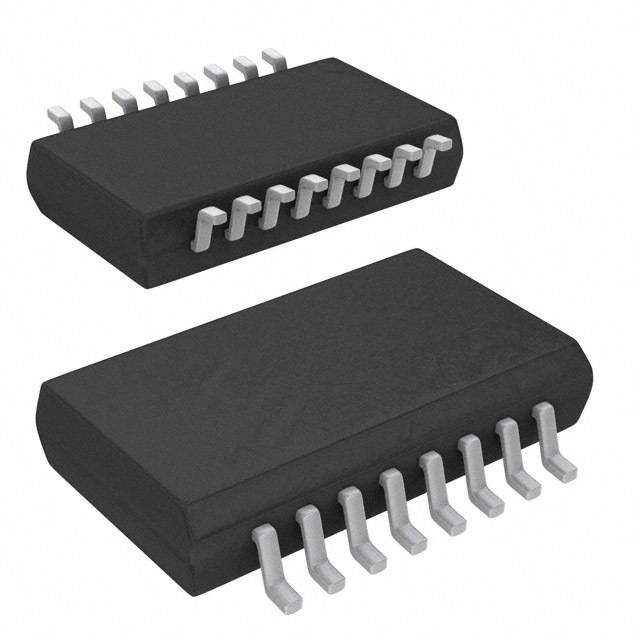
| 产品图片 |
|
| rohs | 符合RoHS无铅 / 符合限制有害物质指令(RoHS)规范要求 |
| 产品系列 | 接口 IC,数字隔离器,Analog Devices ADUM3441CRWZiCoupler® |
| 数据手册 | |
| 产品型号 | ADUM3441CRWZ |
| PulseWidthDistortion(Max) | 2ns |
| 上升/下降时间(典型值) | 2.5ns, 2.5ns |
| 产品目录页面 | |
| 产品种类 | |
| 传播延迟tpLH/tpHL(最大值) | 32ns, 32ns |
| 传播延迟时间 | 32 ns |
| 供应商器件封装 | 16-SOIC W |
| 共模瞬态抗扰度(最小值) | 25kV/µs |
| 其它图纸 |
|
| 包装 | 管件 |
| 商标 | Analog Devices |
| 安装风格 | SMD/SMT |
| 封装 | Tube |
| 封装/外壳 | 16-SOIC(0.295",7.50mm 宽) |
| 封装/箱体 | SOIC-16 |
| 工作温度 | -40°C ~ 105°C |
| 工厂包装数量 | 47 |
| 技术 | 磁耦合 |
| 数据速率 | 150Mbps |
| 最大工作温度 | + 105 C |
| 最大数据速率 | 150 Mb/s |
| 最小工作温度 | - 40 C |
| 标准包装 | 47 |
| 电压-电源 | 3 V ~ 5.5 V |
| 电压-隔离 | 2500Vrms |
| 电源电压-最大 | 5.5 V |
| 电源电压-最小 | 3 V |
| 电源电流 | 1.3 mA |
| 类型 | General Purpose |
| 系列 | ADUM3441 |
| 绝缘电压 | 2.5 kVrms |
| 脉宽失真(最大) | 2ns |
| 视频文件 | http://www.digikey.cn/classic/video.aspx?PlayerID=1364138032001&width=640&height=505&videoID=2219593469001http://www.digikey.cn/classic/video.aspx?PlayerID=1364138032001&width=640&height=505&videoID=2219593470001http://www.digikey.cn/classic/video.aspx?PlayerID=1364138032001&width=640&height=505&videoID=2219614223001 |
| 输入-输入侧1/输入侧2 | 3/1 |
| 通道数 | 4 |
| 通道数量 | 4 Channel |
| 通道类型 | 单向 |
| 隔离式电源 | 无 |


- 商务部:美国ITC正式对集成电路等产品启动337调查
- 曝三星4nm工艺存在良率问题 高通将骁龙8 Gen1或转产台积电
- 太阳诱电将投资9.5亿元在常州建新厂生产MLCC 预计2023年完工
- 英特尔发布欧洲新工厂建设计划 深化IDM 2.0 战略
- 台积电先进制程称霸业界 有大客户加持明年业绩稳了
- 达到5530亿美元!SIA预计今年全球半导体销售额将创下新高
- 英特尔拟将自动驾驶子公司Mobileye上市 估值或超500亿美元
- 三星加码芯片和SET,合并消费电子和移动部门,撤换高东真等 CEO
- 三星电子宣布重大人事变动 还合并消费电子和移动部门
- 海关总署:前11个月进口集成电路产品价值2.52万亿元 增长14.8%


PDF Datasheet 数据手册内容提取
Quad Channel, High Speed Digital Isolators Data Sheet ADuM3440/ADuM3441/ADuM3442 FEATURES FUNCTIONAL BLOCK DIAGRAMS Low power operation VDD1 1 ADuM3440 16VDD2 5 V operation GND1 2 15GND2 1.7 mA per channel maximum @ 0 Mbps to 2 Mbps VIA 3 ENCODE DECODE 14VOA 68 mA per channel maximum @ 150 Mbps VIB 4 ENCODE DECODE 13VOB 3.3 V operation VIC 5 ENCODE DECODE 12VOC 1.0 mA per channel maximum @ 0 Mbps to 2 Mbps VID 6 ENCODE DECODE 11VOD Bidire3c3t mioAna pl ecro cmhmanunneicl amtaioxnim um @ 150 Mbps GNNDC1 87 190VGEN2D2 06837-001 3.3 V/5 V level translation Figure 1. ADuM3440 Functional Block Diagram High temperature operation: 105°C High data rate: dc to 150 Mbps (NRZ) VDD1 1 ADuM3441 16VDD2 Precise timing characteristics GND1 2 15GND2 5 ns maximum pulse width distortion VIA 3 ENCODE DECODE 14VOA 5 ns maximum channel-to-channel matching VIB 4 ENCODE DECODE 13VOB High common-mode transient immunity: >25 kV/μs VIC 5 ENCODE DECODE 12VOC Output enable function VOD 6 DECODE ENCODE 11VID 1Sa6f-eletayd a nSOd IrCe gwuidlaet obroyd ayp pparcokvaaglse GNVDE11 87 190VGEN2D2 06837-002 Figure 2. ADuM3441 Functional Block Diagram UL recognition: 2500 V rms for 1 minute per UL 1577 CSA Component Acceptance Notice #5A VDD1 1 ADuM3442 16VDD2 VDE certificate of conformity GND1 2 15GND2 DIN V VDE V 0884-10 (VDE V 0884-10):2006-12 VIA 3 ENCODE DECODE 14VOA VIORM = 560 V peak VIB 4 ENCODE DECODE 13VOB APPLICATIONS VOC 5 DECODE ENCODE 12VIC VOD 6 DECODE ENCODE 11VID HSPigI hin stperefeadc em/dualttiac hcoannvneerl tiesor liasotiloanti on GNVDE11 87 190VGEN2D2 06837-003 Instrumentation Figure 3. ADuM3442 Functional Block Diagram GENERAL DESCRIPTION The ADuM344x1 are four channel, digital isolators based on the Furthermore, iCoupler devices consume one-tenth to one-sixth Analog Devices, Inc., iCoupler® technology supporting data rates the power of optocouplers at comparable signal data rates. up to 150 Mbps. Combining high speed CMOS and monolithic The ADuM344x isolators provide four independent isolation air core transformer technology, these isolation components channels in a variety of channel configurations (see the provide outstanding performance characteristics superior to Ordering Guide). The ADuM344x operates with the supply alternatives such as optocoupler devices. voltage on either side ranging from 3.0 V to 5.5 V, providing By avoiding the use of LEDs and photodiodes, iCoupler compatibility with lower voltage systems as well as enabling devices remove the design difficulties commonly associated voltage translation functionality across the isolation barrier. In with optocouplers. The typical optocoupler concerns regarding addition, the ADuM344x provides low pulse width distortion uncertain current transfer ratios, nonlinear transfer functions, and tight channel-to-channel matching. Unlike other opto- and temperature and lifetime effects are eliminated with the coupler alternatives, the ADuM344x isolators have a patented simple iCoupler digital interfaces and stable performance refresh feature that ensures dc correctness in the absence of characteristics. The need for external drivers and other discrete input logic transitions and during the power-up/power-down components is eliminated with these iCoupler products. condition. 1 Protected by U.S. Patents 5,952,849; 6,873,065; 6,903,578; and 7,075,329. Rev. D Information furnished by Analog Devices is believed to be accurate and reliable. However, no responsibility is assumed by Analog Devices for its use, nor for any infringements of patents or other One Technology Way, P.O. Box 9106, Norwood, MA 02062-9106, U.S.A. rights of third parties that may result from its use. Specifications subject to change without notice. No license is granted by implication or otherwise under any patent or patent rights of Analog Devices. Tel: 781.329.4700 www.analog.com Trademarks and registered trademarks are the property of their respective owners. Fax: 781.461.3113 ©2007–2012 Analog Devices, Inc. All rights reserved.
ADuM3440/ADuM3441/ADuM3442 Data Sheet TABLE OF CONTENTS Features .............................................................................................. 1 Absolute Maximum Ratings ......................................................... 12 Applications ....................................................................................... 1 ESD Caution................................................................................ 12 Functional Block Diagrams ............................................................. 1 Pin Configurations and Function Descriptions ......................... 13 General Description ......................................................................... 1 Typical Performance Characteristics ........................................... 16 Revision History ............................................................................... 2 Applications Information .............................................................. 18 Specifications ..................................................................................... 3 PC Board Layout ........................................................................ 18 Electrical Characteristics—5 V Operation................................ 3 Propagation Delay-Related Parameters ................................... 18 Electrical Characteristics—3.3 V Operation ............................ 5 System-Level ESD Considerations and Enhancements ........ 18 Electrical Characteristics—Mixed 5 V/3.3 V or 3.3 V/5 V DC Correctness and Magnetic Field Immunity........................... 18 Operation ....................................................................................... 7 Power Consumption .................................................................. 19 Package Characteristics ............................................................. 10 Insulation Lifetime ..................................................................... 20 Regulatory Information ............................................................. 10 Outline Dimensions ....................................................................... 21 Insulation and Safety-Related Specifications .......................... 10 Ordering Guide .......................................................................... 21 DIN V VDE V 0884-10 (VDE V 0884-10) Insulation Characteristics ............................................................................ 11 Recommended Operating Conditions .................................... 11 REVISION HISTORY 2/12—Rev. C to Rev. D 9/08—Rev. A to Rev. B Created Hyperlink for Safety and Regulatory Approvals Changes to Pulse Width Distortion, |t − t | Parameter and PLH PHL Entry in Features Section ................................................................. 1 Channel-to-Channel Matching, Codirectional Channels Change to PC Board Layout Section ............................................ 18 Parameter, Table 1 ............................................................................. 3 Updated Outline Dimensions ....................................................... 21 Changes to Pulse Width Distortion, |t − t | Parameter and PLH PHL Channel-to-Channel Matching, Codirectional Channels 1/09—Rev. B to Rev. C Parameter, Table 2 ............................................................................. 5 Change to Propagation Delay Parameter (Table 1) ...................... 3 Changes to Pulse Width Distortion, |t − t | Parameter and PLH PHL Change to Propagation Delay Parameter (Table 2) ...................... 5 Channel-to-Channel Matching, Codirectional Channels Change to Propagation Delay Parameter (Table 3) ...................... 8 Parameter, Table 3 ............................................................................. 8 5/08—Rev. 0 to Rev. A Changes to Ordering Guide .......................................................... 21 11/07—Rev. 0: Initial Version Rev. D | Page 2 of 24
Data Sheet ADuM3440/ADuM3441/ADuM3442 SPECIFICATIONS ELECTRICAL CHARACTERISTICS—5 V OPERATION All voltages are relative to their respective ground. 4.5 V ≤ V ≤ 5.5 V, 4.5 V ≤ V ≤ 5.5 V. All minimum/maximum specifications DD1 DD2 apply over the entire recommended operation range, unless otherwise noted. All typical specifications are at T = 25°C, V = V = 5 V. A DD1 DD2 Table 1. Parameter Symbol Min Typ Max Unit Test Conditions DC SPECIFICATIONS Input Supply Current per Channel, Quiescent I 0.75 1.3 mA DDI (Q) Output Supply Current per Channel, Quiescent I 0.5 1.2 mA DDO (Q) ADuM3440, Total Supply Current, Four Channels1 DC to 2 Mbps V Supply Current I 3 3.9 mA DC to 1 MHz logic signal frequency DD1 DD1 (Q) V Supply Current I 2 3 mA DC to 1 MHz logic signal frequency DD2 DD2 (Q) 150 Mbps V Supply Current I 120 220 mA 75 MHz logic signal frequency DD1 DD1 (150) V Supply Current I 47 55 mA 75 MHz logic signal frequency DD2 DD2 (150) ADuM3441, Total Supply Current, Four Channels1 DC to 2 Mbps V Supply Current I 2.8 3.6 mA DC to 1 MHz logic signal frequency DD1 DD1 (Q) V Supply Current I 2.3 2.9 mA DC to 1 MHz logic signal frequency DD2 DD2 (Q) 150 Mbps V Supply Current I 101 165 mA 75 MHz logic signal frequency DD1 DD1 (150) V Supply Current I 65 80 mA 75 MHz logic signal frequency DD2 DD2 (150) ADuM3442, Total Supply Current, Four Channels1 DC to 2 Mbps V or V Supply Current I , I 2.5 3.5 mA DC to 1 MHz logic signal frequency DD1 DD2 DD1 (Q) DD2 (Q) 150 Mbps V or V Supply Current I , I 83 130 mA 75 MHz logic signal frequency DD1 DD2 DD1 (150) DD2 (150) For All Models Input Currents I , I , I , −10 +0.01 +10 µA 0 ≤ V , V , V , V ≤ V or V , IA IB IC IA IB IC ID DD1 DD2 I , I , I 0 ≤ V , V ≤ V or V ID E1 E2 E1 E2 DD1 DD2 Logic High Input Threshold V , V 2.0 V IH EH Logic Low Input Threshold V , V 0.8 V IL EL Logic High Output Voltages V , V , (V or 5.0 V I = −20 µA, V = V OAH OBH DD1 Ox Ix IxH V , V V ) − 0.1 OCH ODH DD2 (V or 4.8 V I = −4 mA, V = V DD1 Ox Ix IxH V ) − 0.4 DD2 Logic Low Output Voltages V , V , 0.0 0.1 V I = 20 µA, V = V OAL OBL Ox Ix IxL V , V OCL ODL 0.04 0.1 V I = 400 µA, V = V Ox Ix IxL 0.2 0.4 V I = 4 mA, V = V Ox Ix IxL SWITCHING SPECIFICATIONS Minimum Pulse Width2 PW 6.67 ns C = 15 pF, CMOS signal levels L Maximum Data Rate3 150 Mbps C = 15 pF, CMOS signal levels L Propagation Delay4 t , t 20 32 ns C = 15 pF, CMOS signal levels PHL PLH L Pulse Width Distortion, |t − t |5 PWD 0.5 2 ns C = 15 pF, CMOS signal levels PLH PHL L Change vs. Temperature 3 ps/°C C = 15 pF, CMOS signal levels L Propagation Delay Skew6 t 12 ns C = 15 pF, CMOS signal levels PSK L Channel-to-Channel Matching, t 2 ns C = 15 pF, CMOS signal levels PSKCD L Codirectional Channels5 Channel-to-Channel Matching, t 5 ns C = 15 pF, CMOS signal levels PSKOD L Opposing Directional Channels5 Rev. D | Page 3 of 24
ADuM3440/ADuM3441/ADuM3442 Data Sheet Parameter Symbol Min Typ Max Unit Test Conditions For All Models Output Disable Propagation Delay t , t 6 8 ns C = 15 pF, CMOS signal levels PHZ PLH L (High/Low to High Impedance) Output Enable Propagation Delay t , t 6 8 ns C = 15 pF, CMOS signal levels PZH PZL L (High Impedance to High/Low) Output Rise/Fall Time (10% to 90%) t/t 2.5 ns C = 15 pF, CMOS signal levels R F L Common-Mode Transient Immunity |CM | 25 35 kV/µs V = V or V , V = 1000 V, H Ix DD1 DD2 CM at Logic High Output7 transient magnitude = 800 V Common-Mode Transient Immunity |CM| 25 35 kV/µs V = 0 V, V = 1000 V, L Ix CM at Logic Low Output7 transient magnitude = 800 V Refresh Rate f 1.2 Mbps r Input Dynamic Supply Current per Channel8 I 0.196 mA/Mbps DDI (D) Output Dynamic Supply Current per Channel8 I 0.1 mA/Mbps DDO (D) 1 The supply current values for all four channels are combined when running at identical data rates. Output supply current values are specified with no output load present. The supply current associated with an individual channel operating at a given data rate may be calculated as described in the Power Consumption section. See Figure 8 through Figure 10 for information on per-channel supply current as a function of data rate for unloaded and loaded conditions. See Figure 11 through Figure 15 for total V and V supply currents as a function of data rate for ADuM3440/ADuM3441/ADuM3442 channel configurations. DD1 DD2 2 The minimum pulse width is the shortest pulse width at which the specified pulse width distortion is guaranteed. 3 The maximum data rate is the fastest data rate at which the specified pulse width distortion is guaranteed. 4 t propagation delay is measured from the 50% level of the falling edge of the V signal to the 50% level of the falling edge of the V signal. t propagation delay is PHL Ix Ox PLH measured from the 50% level of the rising edge of the V signal to the 50% level of the rising edge of the V signal. Ix Ox 5 Codirectional channel-to-channel matching is the absolute value of the difference in propagation delays between any two channels with inputs on the same side of the isolation barrier. Opposing-directional channel-to-channel matching is the absolute value of the difference in propagation delays between any two channels with inputs on opposing sides of the isolation barrier. 6 t is the magnitude of the worst-case difference in t or t that is measured between units at the same operating temperature, supply voltages, and output load PSK PHL PLH within the recommended operating conditions. 7 CM is the maximum common-mode voltage slew rate that can be sustained while maintaining V > 0.8 V . CM is the maximum common-mode voltage slew rate H O DDO L that can be sustained while maintaining V < 0.8 V. The common-mode voltage slew rates apply to both rising and falling common-mode voltage edges. The transient O magnitude is the range over which the common mode is slewed. 8 Dynamic supply current is the incremental amount of supply current required for a 1 Mbps increase in signal data rate. See Figure 8 through Figure 10 for information on per-channel supply current for unloaded and loaded conditions. See the Power Consumption section for guidance on calculating the per-channel supply current for a given data rate. Rev. D | Page 4 of 24
Data Sheet ADuM3440/ADuM3441/ADuM3442 ELECTRICAL CHARACTERISTICS—3.3 V OPERATION All voltages are relative to their respective ground. 3.0 V ≤ V ≤ 3.6 V, 3.0 V ≤ V ≤ 3.6 V. All minimum/maximum specifications apply DD1 DD2 over the entire recommended operation range, unless otherwise noted. All typical specifications are at T = 25°C, V = V = 3.3 V. A DD1 DD2 Table 2. Parameter Symbol Min Typ Max Unit Test Conditions DC SPECIFICATIONS Input Supply Current per Channel, Quiescent I 0.43 0.90 mA DDI (Q) Output Supply Current per Channel, Quiescent I 0.3 0.60 mA DDO (Q) ADuM3440, Total Supply Current, Four Channels1 DC to 2 Mbps V Supply Current I 1.7 2.4 mA DC to 1 MHz logic signal frequency DD1 DD1 (Q) V Supply Current I 1.2 1.7 mA DC to 1 MHz logic signal frequency DD2 DD2 (Q) 150 Mbps V Supply Current I 63 110 mA 75 MHz logic signal frequency DD1 DD1 (150) V Supply Current I 17 25 mA 75 MHz logic signal frequency DD2 DD2 (150) ADuM3441, Total Supply Current, Four Channels1 DC to 2 Mbps V Supply Current I 1.6 2.2 mA DC to 1 MHz logic signal frequency DD1 DD1 (Q) V Supply Current I 1.3 1.9 mA DC to 1 MHz logic signal frequency DD2 DD2 (Q) 150 Mbps V Supply Current I 52 80 mA 75 MHz logic signal frequency DD1 DD1 (150) V Supply Current I 29 40 mA 75 MHz logic signal frequency DD2 DD2 (150) ADuM3442, Total Supply Current, Four Channels1 DC to 2 Mbps V or V Supply Current I , I 1.5 2.0 mA DC to 1 MHz logic signal frequency DD1 DD2 DD1 (Q) DD2 (Q) 150 Mbps V or V Supply Current I , I 40 66 mA 75 MHz logic signal frequency DD1 DD2 DD1 (150) DD2 (150) For All Models Input Currents I , I , I , −10 +0.01 +10 µA 0 ≤ V , V , V , V ≤ V or V , IA IB IC IA IB IC ID DD1 DD2 I , I , I 0 ≤ V , V ≤ V or V ID E1 E2 E1 E2 DD1 DD2 Logic High Input Threshold V , V 1.6 V IH EH Logic Low Input Threshold V , V 0.4 V IL EL Logic High Output Voltages V , V , (V or 3.0 V I = −20 µA, V = V OAH OBH DD1 Ox Ix IxH V , V V ) − 0.1 OCH ODH DD2 (V or 2.8 V I = −4 mA, V = V DD1 Ox Ix IxH V ) − 0.4 DD2 Logic Low Output Voltages V , V , 0.0 0.1 V I = 20 µA, V = V OAL OBL Ox Ix IxL V , V OCL ODL 0.04 0.1 V I = 400 µA, V = V Ox Ix IxL 0.2 0.4 V I = 4 mA, V = V Ox Ix IxL SWITCHING SPECIFICATIONS Minimum Pulse Width2 PW 6.67 ns C = 15 pF, CMOS signal levels L Maximum Data Rate3 150 Mbps C = 15 pF, CMOS signal levels L Propagation Delay4 t , t 20 36 ns C = 15 pF, CMOS signal levels PHL PLH L Pulse Width Distortion, |t − t |4 PWD 0.5 2 ns C = 15 pF, CMOS signal levels PLH PHL L Change vs. Temperature 3 ps/°C C = 15 pF, CMOS signal levels L Propagation Delay Skew5 t 16 ns C = 15 pF, CMOS signal levels PSK L Channel-to-Channel Matching, t 2 ns C = 15 pF, CMOS signal levels PSKCD L Codirectional Channels6 Channel-to-Channel Matching, t 5 ns C = 15 pF, CMOS signal levels PSKOD L Opposing Directional Channels5 Rev. D | Page 5 of 24
ADuM3440/ADuM3441/ADuM3442 Data Sheet Parameter Symbol Min Typ Max Unit Test Conditions For All Models Output Disable Propagation Delay t , t 6 8 ns C = 15 pF, CMOS signal levels PHZ PLH L (High/Low to High Impedance) Output Enable Propagation Delay t , t 6 8 ns C = 15 pF, CMOS signal levels PZH PZL L (High Impedance to High/Low) Output Rise/Fall Time (10% to 90%) t/t 3 ns C = 15 pF, CMOS signal levels R F L Common-Mode Transient Immunity |CM | 25 35 kV/µs V = V or V , V = 1000 V, H Ix DD1 DD2 CM at Logic High Output7 transient magnitude = 800 V Common-Mode Transient Immunity |CM| 25 35 kV/µs V = 0 V, V = 1000 V, L Ix CM at Logic Low Output7 transient magnitude = 800 V Refresh Rate f 1.1 Mbps r Input Dynamic Supply Current per Channel8 I 0.076 mA/Mbps DDI (D) Output Dynamic Supply Current per Channel8 I 0.028 mA/Mbps DDO (D) 1 The supply current values for all four channels are combined when running at identical data rates. Output supply current values are specified with no output load present. The supply current associated with an individual channel operating at a given data rate may be calculated as described in the Power Consumption section. See Figure 8 through Figure 10 for information on per-channel supply current as a function of data rate for unloaded and loaded conditions. See Figure 11 through Figure 15 for total V and V supply currents as a function of data rate for ADuM3440/ADuM3441/ADuM3442 channel configurations. DD1 DD2 2 The minimum pulse width is the shortest pulse width at which the specified pulse width distortion is guaranteed. 3 The maximum data rate is the fastest data rate at which the specified pulse width distortion is guaranteed. 4 t propagation delay is measured from the 50% level of the falling edge of the V signal to the 50% level of the falling edge of the V signal. t propagation delay is PHL Ix Ox PLH measured from the 50% level of the rising edge of the V signal to the 50% level of the rising edge of the V signal. Ix Ox 5 t is the magnitude of the worst-case difference in t or t that is measured between units at the same operating temperature, supply voltages, and output load PSK PHL PLH within the recommended operating conditions. 6 Codirectional channel-to-channel matching is the absolute value of the difference in propagation delays between any two channels with inputs on the same side of the isolation barrier. Opposing directional channel-to-channel matching is the absolute value of the difference in propagation delays between any two channels with inputs on opposing sides of the isolation barrier. 7 CM is the maximum common-mode voltage slew rate that can be sustained while maintaining V > 0.8 V . CM is the maximum common-mode voltage slew rate H O DDO L that can be sustained while maintaining V < 0.8 V. The common-mode voltage slew rates apply to both rising and falling common-mode voltage edges. The transient O magnitude is the range over which the common mode is slewed. 8 Dynamic supply current is the incremental amount of supply current required for a 1 Mbps increase in signal data rate. See Figure 8 through Figure 10 for information on per-channel supply current for unloaded and loaded conditions. See the Power Consumption section for guidance on calculating the per-channel supply current for a given data rate. Rev. D | Page 6 of 24
Data Sheet ADuM3440/ADuM3441/ADuM3442 ELECTRICAL CHARACTERISTICS—MIXED 5 V/3.3 V OR 3.3 V/5 V OPERATION All voltages are relative to their respective ground. 5 V/3.3 V operation: 4.5 V ≤ V ≤ 5.5 V, 3.0 V ≤ V ≤ 3.6 V; 3 V/5 V operation: DD1 DD2 3.0 V ≤ V ≤ 3.6 V, 4.5 V ≤ V ≤ 5.5 V. All minimum/maximum specifications apply over the entire recommended operating range, DD1 DD2 unless otherwise noted. All typical specifications are at T = 25°C; V = 3.3 V, V = 5 V or V = 5 V, V = 3.3 V. A DD1 DD2 DD1 DD2 Table 3. Parameter Symbol Min Typ Max Unit Test Conditions DC SPECIFICATIONS Input Supply Current per Channel, Quiescent I DDI (Q) 5 V/3.3 V Operation 0.75 1.3 mA 3.3 V/5 V Operation 0.43 0.9 mA Output Supply Current per Channel, Quiescent I DDO (Q) 5 V/3.3 V Operation 0.3 0.7 mA 3.3 V/5 V Operation 0.5 1.2 mA ADuM3440, Total Supply Current, Four Channels1 DC to 2 Mbps V Supply Current I DD1 DD1 (Q) 5 V/3.3 V Operation 3 3.9 mA DC to 1 MHz logic signal frequency 3.3 V/5 V Operation 1.7 2.4 mA DC to 1 MHz logic signal frequency V Supply Current I DD2 DD2 (Q) 5 V/3.3 V Operation 1.2 1.7 mA DC to 1 MHz logic signal frequency 3.3 V/5 V Operation 2 3 mA DC to 1 MHz logic signal frequency 150 Mbps V Supply Current I DD1 DD1 (150) 5 V/3.3 V Operation 120 220 mA 75 MHz logic signal frequency 3.3 V/5 V Operation 63 110 mA 75 MHz logic signal frequency V Supply Current I DD2 DD2 (150) 5 V/3.3 V Operation 17 25 mA 75 MHz logic signal frequency 3.3 V/5 V Operation 47 55 mA 75 MHz logic signal frequency ADuM3441, Total Supply Current, Four Channels1 DC to 2 Mbps V Supply Current I DD1 DD1 (Q) 5 V/3.3 V Operation 2.8 3.6 mA DC to 1 MHz logic signal frequency 3.3 V/5 V Operation 1.6 2.2 mA DC to 1 MHz logic signal frequency V Supply Current I DD2 DD2 (Q) 5 V/3.3 V Operation 1.3 1.9 mA DC to 1 MHz logic signal frequency 3.3 V/5 V Operation 2.3 2.9 mA DC to 1 MHz logic signal frequency 150 Mbps V Supply Current I DD1 DD1 (150) 5 V/3.3 V Operation 101 165 mA 75 MHz logic signal frequency 3.3 V/5 V Operation 52 80 mA 75 MHz logic signal frequency V Supply Current I DD2 DD2 (150) 5 V/3.3 V Operation 29 40 mA 75 MHz logic signal frequency 3.3 V/5 V Operation 65 80 mA 75 MHz logic signal frequency ADuM3442, Total Supply Current, Four Channels1 DC to 2 Mbps V Supply Current I DD1 DD1 (Q) 5 V/3.3 V Operation 2.5 3.5 mA DC to 1 MHz logic signal frequency 3.3 V/5 V Operation 1.5 2.0 mA DC to 1 MHz logic signal frequency V Supply Current I DD2 DD2 (Q) 5 V/3.3 V Operation 1.5 2.0 mA DC to 1 MHz logic signal frequency 3.3 V/5 V Operation 2.5 3.5 mA DC to 1 MHz logic signal frequency Rev. D | Page 7 of 24
ADuM3440/ADuM3441/ADuM3442 Data Sheet Parameter Symbol Min Typ Max Unit Test Conditions 150 Mbps V Supply Current I DD1 DD1 (150) 5 V/3.3 V Operation 83 130 mA 75 MHz logic signal frequency 3.3 V/5 V Operation 40 66 mA 75 MHz logic signal frequency V Supply Current I DD2 DD2 (150) 5 V/3.3 V Operation 40 66 mA 75 MHz logic signal frequency 3.3 V/5 V Operation 83 130 mA 75 MHz logic signal frequency For All Models Input Currents I , I , I , −10 +0.01 +10 µA 0 ≤ V ,V , V ,V ≤ V or V , IA IB IC IA IB IC ID DD1 DD2 I , I , I 0 ≤ V ,V ≤ V or V ID E1 E2 E1 E2 DD1 DD2 Logic High Input Threshold V , V IH EH 5 V/3.3 V Operation 2.0 V 3.3 V/5 V Operation 1.6 V Logic Low Input Threshold V , V IL EL 5 V/3.3 V Operation 0.8 V 3.3 V/5 V Operation 0.4 V Logic High Output Voltages V , V , (V or (V or V I = −20 µA, V = V OAH OBH DD1 DD1 Ox Ix IxH V , V V ) − 0.1 V ) OCH ODH DD2 DD2 (V or (V or V I = −4 mA, V = V DD1 DD1 Ox Ix IxH V ) − 0.4 V ) − 0.2 DD2 DD2 Logic Low Output Voltages V , V , 0.0 0.1 V I = 20 µA, V = V OAL OBL Ox Ix IxL V , V OCL ODL 0.04 0.1 V I = 400 µA, V = V Ox Ix IxL 0.2 0.4 V I = 4 mA, V = V Ox Ix IxL SWITCHING SPECIFICATIONS Minimum Pulse Width2 PW 6.67 ns C = 15 pF, CMOS signal levels L Maximum Data Rate3 150 Mbps C = 15 pF, CMOS signal levels L Propagation Delay4 t , t 20 35 ns C = 15 pF, CMOS signal levels PHL PLH L Pulse Width Distortion, |t − t |4 PWD 0.5 2 ns C = 15 pF, CMOS signal levels PLH PHL L Change vs. Temperature 3 ps/°C C = 15 pF, CMOS signal levels L Propagation Delay Skew5 t 15 ns C = 15 pF, CMOS signal levels PSK L Channel-to-Channel Matching, t 2 ns C = 15 pF, CMOS signal levels PSKCD L Codirectional Channels6 Channel-to-Channel Matching, t 5 ns C = 15 pF, CMOS signal levels PSKOD L Opposing Directional Channels5 For All Models Output Disable Propagation Delay t , t 6 8 ns C = 15 pF, CMOS signal levels PHZ PLH L (High/Low to High Impedance) Output Enable Propagation Delay t , t 6 8 ns C = 15 pF, CMOS signal levels PZH PZL L (High Impedance to High/Low) Output Rise/Fall Time (10% to 90%) t/t C = 15 pF, CMOS signal levels R F L 5 V/3 V Operation 3.0 ns 3 V/5 V Operation 2.5 ns Common-Mode Transient Immunity |CM | 25 35 kV/µs V = V or V , V = 1000 V, H Ix DD1 DD2 CM at Logic High Output7 transient magnitude = 800 V Common-Mode Transient Immunity |CM| 25 35 kV/µs V = 0 V, V = 1000 V, L Ix CM at Logic Low Output7 transient magnitude = 800 V Refresh Rate f r 5 V/3.3 V Operation 1.2 Mbps 3.3 V/5 V Operation 1.1 Mbps Input Dynamic Supply Current per Channel8 I DDI (D) 5 V/3.3 V Operation 0.196 mA/Mbps 3.3 V/5 V Operation 0.076 mA/Mbps Output Dynamic Supply Current per Channel8 I DDO (D) 5 V/3.3 V Operation 0.028 mA/Mbps 3.3 V/5 V Operation 0.01 mA/Mbps Rev. D | Page 8 of 24
Data Sheet ADuM3440/ADuM3441/ADuM3442 1 The supply current values for all four channels are combined when running at identical data rates. Output supply current values are specified with no output load present. The supply current associated with an individual channel operating at a given data rate may be calculated as described in the Power Consumption section. See Figure 8 through Figure 10 for information on per-channel supply current as a function of data rate for unloaded and loaded conditions. See Figure 11 through Figure 15 for total V and V supply currents as a function of data rate for ADuM3440/ADuM3441/ADuM3442 channel configurations. DD1 DD2 2 The minimum pulse width is the shortest pulse width at which the specified pulse width distortion is guaranteed. 3 The maximum data rate is the fastest data rate at which the specified pulse width distortion is guaranteed. 4 t propagation delay is measured from the 50% level of the falling edge of the V signal to the 50% level of the falling edge of the V signal. t propagation delay is PHL Ix Ox PLH measured from the 50% level of the rising edge of the V signal to the 50% level of the rising edge of the V signal. Ix Ox 5 t is the magnitude of the worst-case difference in t or t that is measured between units at the same operating temperature, supply voltages, and output load PSK PHL PLH within the recommended operating conditions. 6 Codirectional channel-to-channel matching is the absolute value of the difference in propagation delays between any two channels with inputs on the same side of the isolation barrier. Opposing directional channel-to-channel matching is the absolute value of the difference in propagation delays between any two channels with inputs on opposing sides of the isolation barrier. 7 CM is the maximum common-mode voltage slew rate that can be sustained while maintaining V > 0.8 V . CM is the maximum common-mode voltage slew rate H O DDO L that can be sustained while maintaining V < 0.8 V. The common-mode voltage slew rates apply to both rising and falling common-mode voltage edges. The transient O magnitude is the range over which the common mode is slewed. 8 Dynamic supply current is the incremental amount of supply current required for a 1 Mbps increase in signal data rate. See Figure 8 through Figure 10 for information on per-channel supply current for unloaded and loaded conditions. See the Power Consumption section for guidance on calculating the per-channel supply current for a given data rate. Rev. D | Page 9 of 24
ADuM3440/ADuM3441/ADuM3442 Data Sheet PACKAGE CHARACTERISTICS Table 4. Parameter Symbol Min Typ Max Unit Test Conditions Resistance (Input to Output)1 R 1012 Ω I-O Capacitance (Input to Output)1 C 2.2 pF f = 1 MHz I-O Input Capacitance2 C 4.0 pF I IC Junction-to-Case Thermal Resistance, Side 1 θ 33 °C/W Thermocouple located at JCI IC Junction-to-Case Thermal Resistance, Side 2 θ 28 °C/W center of package underside JCO 1 The device is considered a 2-terminal device; Pin 1 through Pin 8 are shorted together and Pin 9 through Pin 16 are shorted together. 2 Input capacitance is from any input data pin to ground. REGULATORY INFORMATION The ADuM344x is approved by the organizations listed in Table 5. Refer to Table 10 and the Insulation Lifetime section for details regarding recommended maximum working voltages for specific cross-isolation waveforms and insulation levels. Table 5. UL CSA VDE Recognized under Approved under Certified according to 1577 component recognition program1 CSA Component Acceptance Notice #5A DIN V VDE V 0884-10 (VDE V 0884-10):2006-122 Single protection, Basic insulation per CSA 60950-1-03 and Reinforced insulation, 560 V peak 2500 V rms isolation voltage IEC 60950-1, 800 V rms (1131 V peak) maximum working voltage Reinforced insulation per CSA 60950-1-03 and IEC 60950-1, 400 V rms (566 V peak) maximum working voltage File E214100 File 205078 File 2471900-4880-0001 1 In accordance with UL 1577, each ADuM344x is proof tested by applying an insulation test voltage ≥3000 V rms for 1 sec (current leakage detection limit = 5 µA). 2 In accordance with DIN V VDE V 0884-10, each ADuM344x is proof tested by applying an insulation test voltage ≥1050 V peak for 1 sec (partial discharge detection limit = 5 pC). An asterisk (*) marking branded on the component designates DIN V VDE V 0884-10 approval. INSULATION AND SAFETY-RELATED SPECIFICATIONS Table 6. Parameter Symbol Value Unit Conditions Rated Dielectric Insulation Voltage 2500 V rms 1-minute duration Minimum External Air Gap (Clearance) L(I01) 7.7 min mm Measured from input terminals to output terminals, shortest distance through air Minimum External Tracking (Creepage) L(I02) 8.1 min mm Measured from input terminals to output terminals, shortest distance path along body Minimum Internal Gap (Internal Clearance) 0.017 min mm Insulation distance through insulation Tracking Resistance (Comparative Tracking Index) CTI >175 V DIN IEC 112/VDE 0303 Part 1 Isolation Group IIIa Material Group (DIN VDE 0110, 1/89, Table 1) Rev. D | Page 10 of 24
Data Sheet ADuM3440/ADuM3441/ADuM3442 DIN V VDE V 0884-10 (VDE V 0884-10) INSULATION CHARACTERISTICS These isolators are suitable for reinforced electrical isolation only within the safety limit data. Maintenance of the safety data is ensured by protective circuits. The asterisk (*) marking on packages denotes DIN V VDE V 0884-10 approval. Table 7. Description Conditions Symbol Characteristic Unit Installation Classification per DIN VDE 0110 For Rated Mains Voltage ≤ 150 V rms I to IV For Rated Mains Voltage ≤ 300 V rms I to III For Rated Mains Voltage ≤ 400 V rms I to II Climatic Classification 40/105/21 Pollution Degree per DIN VDE 0110, Table 1 2 Maximum Working Insulation Voltage V 560 V peak IORM Input-to-Output Test Voltage, Method B1 V × 1.875 = V , 100% production test, t = 1 sec, V 1050 V peak IORM PR m PR partial discharge < 5 pC Input-to-Output Test Voltage, Method A V × 1.6 = V , t = 60 sec, partial discharge < 5 pC V IORM PR m PR After Environmental Tests Subgroup 1 896 V peak After Input and/or Safety Test V × 1.2 = V , t = 60 sec, partial discharge < 5 pC 672 V peak IORM PR m Subgroup 2 and Subgroup 3 Highest Allowable Overvoltage Transient overvoltage, t = 10 seconds V 4000 V peak TR TR Safety-Limiting Values Maximum value allowed in the event of a failure (see Figure 4) Case Temperature T 150 °C S Side 1 Current I 265 mA S1 Side 2 Current I 335 mA S2 Insulation Resistance at T V = 500 V R >109 Ω S IO S 350 RECOMMENDED OPERATING CONDITIONS 300 Table 8. A) m Parameter Rating T ( 250 N Operating Temperature Range, T −40°C to +105°C E SIDE #2 A R UR 200 Supply Voltage Range, VDD1, VDD21 3.0 V to 5.5 V C G Input Signal Rise and Fall Time 1.0 ms N TI 150 1 All voltages are relative to their respective ground. See the DC Correctness LIMI SIDE #1 and Magnetic Field Immunity section for information on immunity to external Y- 100 magnetic fields. T E AF S 50 00 50CASE TEMP1E0R0ATURE (°C)150 200 06837-004 Figure 4. Thermal Derating Curve, Dependence of Safety-Limiting Values with Case Temperature per DIN V VDE V 0884-10 Rev. D | Page 11 of 24
ADuM3440/ADuM3441/ADuM3442 Data Sheet ABSOLUTE MAXIMUM RATINGS Ambient temperature = 25°C, unless otherwise noted. Stresses above those listed under Absolute Maximum Ratings may cause permanent damage to the device. This is a stress Table 9. rating only; functional operation of the device at these or any Parameter Rating other conditions above those indicated in the operational Storage Temperature Range (T ) −65°C to +150°C ST section of this specification is not implied. Exposure to absolute Ambient Operating Temperature Range (T) −40°C to +105°C A maximum rating conditions for extended periods may affect Supply Voltages (V , V )1 −0.5 V to +7.0 V DD1 DD2 device reliability. Input Voltage (V , V , V , V , V , V )1, 2 −0.5 V to V + 0.5 V IA IB IC ID E1 E2 DD1 Output Voltage (V , V , V , V )1, 2 −0.5 V to V + 0.5 V OA OB OC OD DDO Average Output Current per Pin3 ESD CAUTION Side 1 (I ) −18 mA to +18 mA O1 Side 2 (I ) −22 mA to +22 mA O2 Common-Mode Transients (CM , CM)4 −100 kV/µs to H L +100 kV/µs 1 All voltages are relative to their respective ground. 2 V and V refer to the supply voltages on the input and output sides of a DDI DDO given channel, respectively. See the PC Board Layout section. 3 See Figure 4 for maximum rated current values for various temperatures. 4 Refers to common-mode transients across the insulation barrier. Common- mode transients exceeding the Absolute Maximum Ratings can cause latch- up or permanent damage. Table 10. Maximum Continuous Working Voltage1 Parameter Max Unit Constraint AC Voltage, Bipolar Waveform 565 V peak 50-year minimum lifetime AC Voltage, Unipolar Waveform Basic Insulation 1131 V peak Maximum approved working voltage per IEC 60950-1 Reinforced Insulation 560 V peak Maximum approved working voltage per IEC 60950-1 and VDE V 0884-10 DC Voltage Basic Insulation 1131 V peak Maximum approved working voltage per IEC 60950-1 Reinforced Insulation 560 V peak Maximum approved working voltage per IEC 60950-1 and VDE V 0884-10 1 Refers to continuous voltage magnitude imposed across the isolation barrier. See the Insulation Lifetime section for more details. Table 11. Truth Table (Positive Logic) V Input1 V Input2 V State1 V State1 V Output1 Notes IX EX DDI DDO OX H H or NC Powered Powered H L H or NC Powered Powered L X L Powered Powered Z X H or NC Unpowered Powered H Outputs return to the input state within 1 µs of V power restoration. DDI X L Unpowered Powered Z X X Powered Unpowered Indeterminate Outputs return to the input state within 1 µs of V power DDO restoration if V state is H or NC. Outputs return to high impedance EX state within 8 ns of V power restoration if V state is L. DDO EX 1 V and V refer to the input and output signals of a given channel (A, B, C, or D). V refers to the output enable signal on the same side as the V outputs. V and IX OX EX OX DDI V refer to the supply voltages on the input and output sides of the given channel, respectively. DDO 2 In noisy environments, connecting V to an external logic high or low is recommended. EX Rev. D | Page 12 of 24
Data Sheet ADuM3440/ADuM3441/ADuM3442 PIN CONFIGURATIONS AND FUNCTION DESCRIPTIONS VDD1 1 16 VDD2 GND1* 2 15 GND2* VIA 3 ADuM3440 14 VOA VIB 4 TOP VIEW 13 VOB VIC 5 (Not to Scale) 12 VOC VID 6 11 VOD NC 7 10 VE2 GND1* 8 9 GND2* NC = NO CONNECT * GCPOINNDN 21N AEISCN RTDIE NPCGINO BM8O MATERHNE TD IONETD GE. NRPDNIN2A I9LS LA RYNE DCC OPONIMNN M1E5EC NATDEREDED AI.NNTDE RCNOANLNLEYC CTIONNGN BEOCTTHE DT OAND 06837-005 Figure 5. ADuM3440 Pin Configuration Table 12. ADuM3440 Pin Function Descriptions Pin No. Mnemonic Description 1 V Supply Voltage for Isolator Side 1, 3.0 V to 5.5 V. DD1 2, 8 GND Ground 1. Ground reference for Isolator Side 1. 1 3 V Logic Input A. IA 4 V Logic Input B. IB 5 V Logic Input C. IC 6 V Logic Input D. ID 7 NC No Connect. 9, 15 GND Ground 2. Ground reference for Isolator Side 2. 2 10 V Output Enable 2. Active high logic input. V , V , V , and V outputs are enabled when V is high or disconnected. E2 OA OB OC OD E2 V , V , V , and V outputs are disabled when V is low. In noisy environments, connecting V to an external OA OB OC OD E2 E2 logic high or low is recommended. 11 V Logic Output D. OD 12 V Logic Output C. OC 13 V Logic Output B. OB 14 V Logic Output A. OA 16 V Supply Voltage for Isolator Side 2, 3.0 V to 5.5 V. DD2 Rev. D | Page 13 of 24
ADuM3440/ADuM3441/ADuM3442 Data Sheet VDD1 1 16 VDD2 GND1* 2 15 GND2* VIA 3 ADuM3441 14 VOA VIB 4 TOP VIEW 13 VOB VIC 5 (Not to Scale) 12 VOC VOD 6 11 VID VE1 7 10 VE2 GND1* 8 9 GND2* * GCPOINNDN 21N AEISCN RTDIE NPCGINO BM8O MATERHNE TD IONETD GE. NRPDNIN2A I9LS LA RYNE DCC OPONIMNN M1E5EC NATDEREDED AI.NNTDE RCNOANLNLEYC CTIONNGN BEOCTTHE DT OAND 06837-006 Figure 6. ADuM3441 Pin Configuration Table 13. ADuM3441 Pin Function Descriptions Pin No. Mnemonic Description 1 V Supply Voltage for Isolator Side 1, 3.0 V to 5.5 V. DD1 2, 8 GND Ground 1. Ground reference for Isolator Side 1. 1 3 V Logic Input A. IA 4 V Logic Input B. IB 5 V Logic Input C. IC 6 V Logic Output D. OD 7 V Output Enable 1. Active high logic input. V output is enabled when V is high or disconnected. V is disabled E1 OD E1 OD when V is low. In noisy environments, connecting V to an external logic high or low is recommended. E1 E1 9, 15 GND Ground 2. Ground reference for Isolator Side 2. 2 10 V Output Enable 2. Active high logic input. V , V , and V outputs are enabled when V is high or disconnected. V , E2 OA OB OC E2 OA V , and V outputs are disabled when V is low. In noisy environments, connecting V to an external logic high or OB OC E2 E2 low is recommended. 11 V Logic Input D. ID 12 V Logic Output C. OC 13 V Logic Output B. OB 14 V Logic Output A. OA 16 V Supply Voltage for Isolator Side 1, 3.0 V to 5.5 V. DD2 Rev. D | Page 14 of 24
Data Sheet ADuM3440/ADuM3441/ADuM3442 VDD1 1 16 VDD2 GND1* 2 15 GND2* VIA 3 ADuM3442 14 VOA VIB 4 TOP VIEW 13 VOB VOC 5 (Not to Scale) 12 VIC VOD 6 11 VID VE1 7 10 VE2 GND1* 8 9 GND2* * GCPOINNDN 21N AEISCN RTDIE NPCGINO BM8O MATERHNE TD IONETD GE. NRPDNIN2A I9LS LA RYNE DCC OPONIMNN M1E5EC NATDEREDED AI.NNTDE RCNOANLNLEYC CTIONNGN BEOCTTHE DT OAND 06837-007 Figure 7. ADuM3442 Pin Configuration Table 14. ADuM3442 Pin Function Descriptions Pin No. Mnemonic Function 1 V Supply Voltage for Isolator Side 1, 3.0 V to 5.5 V. DD1 2, 8 GND Ground 1. Ground reference for Isolator Side 1. 1 3 V Logic Input A. IA 4 V Logic Input B. IB 5 V Logic Output C. OC 6 V Logic Output D. OD 7 V Output Enable 1. Active high logic input. V and V outputs are enabled when V is high or disconnected. V and E1 OC OD E1 OC V outputs are disabled when V is low. In noisy environments, connecting V to an external logic high or low is OD E1 E1 recommended. 9, 15 GND Ground 2. Ground reference for Isolator Side 2. 2 10 V Output Enable 2. Active high logic input. V and V outputs are enabled when V is high or disconnected. V and E2 OA OB E2 OA V outputs are disabled when V is low. In noisy environments, connecting V to an external logic high or low is OB E2 E2 recommended. 11 V Logic Input D. ID 12 V Logic Input C. IC 13 V Logic Output B. OB 14 V Logic Output A. OA 16 V Supply Voltage for Isolator Side 2, 3.0 V to 5.5 V. DD2 Rev. D | Page 15 of 24
ADuM3440/ADuM3441/ADuM3442 Data Sheet TYPICAL PERFORMANCE CHARACTERISTICS 35 140 30 120 mA) 25 100 RENT/CHANNEL ( 2105 5V CURRENT (mA) 8600 5V R U 10 40 C 3.3V 3.3V 5 20 00 50DATA RATE (Mbps1)00 150 06837-008 00 50DATA RATE (Mbps1)00 150 06837-011 Figure 8. Typical Input Supply Current per Channel vs. Data Rate Figure 11. Typical ADuM3440 V Supply Current vs. Data Rate DD1 for 5 V and 3.3 V Operation for 5 V and 3.3 V Operation 14 50 45 12 40 mA) 10 35 NT/CHANNEL ( 68 5V URRENT (mA) 223050 5V RE C UR 4 15 C 3.3V 10 3.3V 2 5 00 50DATA RATE (Mbps1)00 150 06837-009 00 50DATA RATE (Mbps1)00 150 06837-012 Figure 9. Typical Output Supply Current per Channel vs. Data Rate Figure 12. Typical ADuM3440 V Supply Current vs. Data Rate DD2 for 5 V and 3.3 V Operation (No Output Load) for 5 V and 3.3 V Operation 20 120 18 100 16 A) m 14 NEL ( 12 mA) 80 RENT/CHAN 108 5V CURRENT ( 4600 5V R 6 U C 3.3V 3.3V 4 20 2 000 50DATA RATE (Mbps1)00 150 06837-010 00 50DATA RATE (Mbps1)00 150 06837-013 Figure 10. Typical Output Supply Current per Channel vs. Data Rate Figure 13. Typical ADuM3441 V Supply Current vs. Data Rate DD1 for 5 V and 3.3 V Operation (15 pF Output Load) for 5 V and 3.3 V Operation Rev. D | Page 16 of 24
Data Sheet ADuM3440/ADuM3441/ADuM3442 70 90 80 60 70 50 60 A) A) NT (m 40 5V NT (m 50 5V E E RR 30 RR 40 U U C C 30 20 3.3V 3.3V 20 10 10 00 50DATA RATE (Mbps1)00 150 06837-014 00 50DATA RATE (Mbps1)00 150 06837-015 Figure 14. Typical ADuM3441 V Supply Current vs. Data Rate Figure 15. Typical ADuM3442 V or V Supply Current vs.Data Rate DD2 DD1 DD2 for 5 V and 3.3 V Operation for 5 V and 3.3 V Operation Rev. D | Page 17 of 24
ADuM3440/ADuM3441/ADuM3442 Data Sheet APPLICATIONS INFORMATION PC BOARD LAYOUT SYSTEM-LEVEL ESD CONSIDERATIONS AND ENHANCEMENTS The ADuM344x digital isolator requires no external interface circuitry for the logic interfaces. Power supply bypassing is System-level ESD reliability (for example, per IEC 61000-4-x) strongly recommended at the input and output supply pins (see is highly dependent on system design, which varies widely by Figure 16). Bypass capacitors are most conveniently connected application. The ADuM344x incorporate many enhancements between Pin 1 and Pin 2 for V and between Pin 15 and Pin 16 to make ESD reliability less dependent on system design. The DD1 for V . The capacitor value should be between 0.01 μF and 0.1 μF. enhancements include the following: DD2 The total lead length between both ends of the capacitor and ESD protection cells added to all input/output interfaces. the input power supply pin should not exceed 20 mm. Bypassing Key metal trace resistances reduced using wider geometry between Pin 1 and Pin 8 and between Pin 9 and Pin 16 should and paralleling of lines with vias. be considered unless the ground pair on each package side is connected close to the package. The SCR effect inherent in CMOS devices is minimized by the use of guarding and isolation techniques between VDD1 VDD2 GND1 GND2 PMOS and NMOS devices. VIA VOA VIB VOB Areas of high electric field concentration eliminated using VIC/OC VOC/IC 45° corners on metal traces. VGIDNV/ODED11 VVGOEN2DD/I2D 06837-017 Supply pin overvoltage prevented with larger ESD clamps Figure 16. Recommended Printed Circuit Board Layout between each supply pin and its respective ground. In applications involving high common-mode transients, care While the ADuM344x improve system-level ESD reliability, should be taken to ensure that board coupling across the isolation they are no substitute for a robust system-level design. See the barrier is minimized. Furthermore, the board layout should be AN-793 application note, ESD/Latch-Up Considerations with designed such that any coupling that does occur equally affects iCoupler Isolation Products for detailed recommendations on all pins on a given component side. Failure to ensure this could board layout and system-level design. cause voltage differentials between pins exceeding the device’s DC CORRECTNESS AND MAGNETIC FIELD IMMUNITY absolute maximum ratings, thereby leading to latch-up or Positive and negative logic transitions at the isolator input cause permanent damage. narrow (~1 ns) pulses to be sent to the decoder via the transformer. See the AN-1109 Application Note for board layout guidelines. The decoder is bistable and is, therefore, either set or reset by PROPAGATION DELAY-RELATED PARAMETERS the pulses, indicating input logic transitions. In the absence of logic transitions at the input for more than ~1 μs, a periodic set Propagation delay is a parameter that describes the time it takes of refresh pulses indicative of the correct input state are sent to a logic signal to propagate through a component. The propagation ensure dc correctness at the output. If the decoder receives no delay to a logic low output may differ from the propagation internal pulses of more than about 5 μs, the input side is assumed delay to a logic high. unpowered or nonfunctional, in which case the isolator output INPUT (VIx) 50% is forced to a default state (see the Absolute Maximum Ratings section) by the watchdog timer circuit. tPLH tPHL OUTPUT (VOx) 50% 06837-018 Tish see tl ibmyi ttahteio cno nond itthioen m inag wnhetiicch f iienlddu imcemd uvonlittayg oef itnh eth AeD reucMei3v4in4gx Figure 17. Propagation Delay Parameters coil of the transformer is sufficiently large to either falsely set or reset the decoder. The following analysis defines the conditions Pulse width distortion is the maximum difference between under which this can occur. The 3 V operating condition of the these two propagation delay values and is an indication of how ADuM344x is examined because it represents the most susceptible accurately the input signal’s timing is preserved. mode of operation. Channel-to-channel matching refers to the maximum amount The pulses at the transformer output have an amplitude greater the propagation delay differs between channels within a single than 1.0 V. The decoder has a sensing threshold at about 0.5 V, ADuM344x component. thus establishing a 0.5 V margin in which induced voltages can Propagation delay skew refers to the maximum amount the be tolerated. propagation delay differs between multiple ADuM344x components operating under the same conditions. Rev. D | Page 18 of 24
Data Sheet ADuM3440/ADuM3441/ADuM3442 The voltage induced across the receiving coil is given by 1000 V = (−dβ/dt)∑ πr 2; n = 1, 2, … , N A) DISTANCE = 1m n T (k 100 where: EN R β is magnetic flux density (gauss). UR C N is the number of turns in the receiving coil. E 10 L r is the radius of the nth turn in the receiving coil (cm). AB DISTANCE = 100mm n W O Given the geometry of the receiving coil in the ADuM344x and L 1 L A an imposed requirement that the induced voltage be at most M DISTANCE = 5mm U 50% of the 0.5 V margin at the decoder, a maximum allowable XIM 0.1 A magnetic field is calculated as shown in Figure 18. M 100 0.01 C FLUX 10 1k 10MkAGNET1IC0 0FkIELD FRE1QMUENCY (H1z0)M 100M 06837-020 TI Figure 19. Maximum Allowable Current E N for Various Current-to-ADuM344x Spacings AGss) E Mgau 1 Note that at combinations of strong magnetic field and high Lk ABY ( frequency, any loops formed by printed circuit board traces ALLOWDENSIT0.1 cthoeu ltdh riensdhuocled se rorfo sru vcocleteadgiensg s ucifrficcuieitnrtyl.y C laarrge es henououldg hb et ota tkreigng ienr M U the layout of such traces to avoid this possibility. XIM 0.01 A POWER CONSUMPTION M 0.0011k 10kMAGNETI1C0 0FkIELD FREQ1MUENCY (Hz1)0M 100M 06837-019 Tisholea stourp pisl ya cfuunrrcetniot na to af tghivee snu pchpalyn nvoellt oafg eth, teh Ae DchuaMnn3e4l4’sx d ata rate, and the channel’s output load. Figure 18. Maximum Allowable External Magnetic Flux Density For each input channel, the supply current is given by For example, at a magnetic field frequency of 1 MHz, the maximum allowable magnetic field of 0.2 kgauss induces a I = I f ≤ 0.5 f DDI DDI (Q) r voltage of 0.25 V at the receiving coil. This is about 50% of the I = I × (2f − f) + I f > 0.5 f DDI DDI (D) r DDI (Q) r sensing threshold and does not cause a faulty output transition. For each output channel, the supply current is given by Similarly, if such an event were to occur during a transmitted pulse (and was of the worst-case polarity), it would reduce the I = I f ≤ 0.5 f DDO DDO (Q) r received pulse from >1.0 V to 0.75 V—still well above the 0.5 V I = (I + (0.5 × 10⁻³) × C × V ) × (2f − f) + I DDO DDO (D) L DDO r DDO (Q) sensing threshold of the decoder. f > 0.5 f r The preceding magnetic flux density values correspond to where: specific current magnitudes at given distances from the I , I are the input and output dynamic supply currents DDI (D) DDO (D) ADuM344x transformers. Figure 19 expresses these allowable per channel (mA/Mbps). current magnitudes as a function of frequency for selected C is the output load capacitance (pF). L distances. As shown, the ADuM344x is extremely immune V is the output supply voltage (V). DDO and can be affected only by extremely large currents operated f is the input logic signal frequency (MHz); it is half of the input at high frequency very close to the component. For the 1 MHz data rate expressed in units of Mbps. example noted, one would have to place a 0.5 kA current 5 mm f is the input stage refresh rate (Mbps). r away from the ADuM344x to affect the component’s operation. I , I are the specified input and output quiescent DDI (Q) DDO (Q) supply currents (mA). To calculate the total V and V supply current, the supply DD1 DD2 currents for each input and output channel corresponding to V and V are calculated and totaled. Figure 8 and Figure 9 DD1 DD2 provide per-channel supply currents as a function of data rate for an unloaded output condition. Figure 10 provides per- channel supply current as a function of data rate for a 15 pF output condition. Figure 11 through Figure 15 provide total V and V supply current as a function of data rate for DD1 DD2 ADuM3440/ADuM3441/ADuM3442 channel configurations. Rev. D | Page 19 of 24
ADuM3440/ADuM3441/ADuM3442 Data Sheet INSULATION LIFETIME In the case of unipolar ac or dc voltage, the stress on the insulation is significantly lower, which allows operation at higher working All insulation structures eventually break down when subjected voltages while still achieving a 50-year service life. The working to voltage stress over a sufficiently long period. The rate of voltages listed in Table 10 can be applied while maintaining the insulation degradation is dependent on the characteristics of 50-year minimum lifetime provided the voltage conforms to the voltage waveform applied across the insulation. In addition either the unipolar ac or dc voltage cases. Any cross insulation to the testing performed by the regulatory agencies, Analog voltage waveform that does not conform to Figure 21 or Figure 22 Devices carries out an extensive set of evaluations to determine should be treated as a bipolar ac waveform and its peak voltage the lifetime of the insulation structure within the ADuM344x. should be limited to the 50-year lifetime voltage value listed in Analog Devices performs accelerated life testing using voltage levels Table 10. higher than the rated continuous working voltage. Acceleration Note that the voltage presented in Figure 21 is shown as sinusoidal factors for several operating conditions are determined. These for illustration purposes only. It is meant to represent any voltage factors allow calculation of the time to failure at the actual working waveform varying between 0 V and some limiting value. The voltage. The values shown in Figure 20 summarize the peak voltage limiting value can be positive or negative, but the voltage cannot for 50 years of service life for a bipolar ac operating condition, and cross 0 V. the maximum CSA/VDE approved working voltages. In many cases, the approved working voltage is higher than the 50-year RATED PEAK VOLTAGE scearnv liecaed li tfeo vsholotratgeen. eOdp ienrsautliaotnio ant ltihfee sien hsoigmh ew coarskeisn. g voltages 0V 06837-021 Figure 20. Bipolar AC Waveform The insulation lifetime of the ADuM344x depends on the voltage waveform type imposed across the isolation barrier. The iCoupler insulation structure degrades at different rates RATED PEAK VOLTAGE depending on whether the waveform is bipolar ac, unipolar ac, odrif dfecr.e Fnitg iusroela 2ti0o, nF ivgoulrtaeg 2e1 w, aanvdef Forigmusr.e 22 illustrate these 0V 06837-022 Figure 21. Unipolar AC Waveform Bipolar ac voltage is the most stringent environment. The goal of a 50-year operating lifetime under the ac bipolar condition determines the maximum working voltage recommended by RATED PEAK VOLTAGE Analog Devices. 0V 06837-023 Figure 22. DC Waveform Rev. D | Page 20 of 24
Data Sheet ADuM3440/ADuM3441/ADuM3442 OUTLINE DIMENSIONS 10.50(0.4134) 10.10(0.3976) 16 9 7.60(0.2992) 7.40(0.2913) 1 8 10.65(0.4193) 10.00(0.3937) 1.27(0.0500) 0.75(0.0295) BSC 2.65(0.1043) 0.25(0.0098) 45° 0.30(0.0118) 2.35(0.0925) 8° 0.10(0.0039) 0° COPLANARITY 0.10 0.51(0.0201) SPELAATNIENG 0.33(0.0130) 1.27(0.0500) 0.31(0.0122) 0.20(0.0079) 0.40(0.0157) C(RINOEFNPEATRRREOENNLCLTEIHNCEOGOSNDMELISPYM)LAEAIANNRNDSETIAORTRNOOESUJNANEORDDETEEDAICN-POSMPFTRIFALONLMPIDMIRLAELIRATIMTDEEESRTFSMEO;SRIRN-0ECU1QH3SU-EADIVAIINMAELDENENSSTIIOGSNNFS.OR 03-27-2007-B Figure 23. 16-Lead Standard Small Outline Package [SOIC_W] Wide Body (RW-16) Dimensions shown in millimeters and (inches) ORDERING GUIDE Number of Number of Maximum Maximum Maximum Inputs, Inputs, Data Rate Propagation Pulse Width Temperature Package Package Model1, 2 V Side V Side (Mbps) Delay, 5 V (ns) Distortion (ns) Range Description Option DD1 DD2 ADuM3440CRWZ 4 0 150 32 2 −40°C to +105°C 16-Lead SOIC_W RW-16 ADuM3441CRWZ 3 1 150 32 2 −40°C to +105°C 16-Lead SOIC_W RW-16 ADuM3442CRWZ 2 2 150 32 2 −40°C to +105°C 16-Lead SOIC_W RW-16 1 Z = RoHS Compliant Part. 2 Tape and reel are available. The addition of an -RL suffix designates a 13” (1,000 units) tape-and-reel option. Rev. D | Page 21 of 24
ADuM3440/ADuM3441/ADuM3442 Data Sheet NOTES Rev. D | Page 22 of 24
Data Sheet ADuM3440/ADuM3441/ADuM3442 NOTES Rev. D | Page 23 of 24
ADuM3440/ADuM3441/ADuM3442 Data Sheet NOTES ©2007–2012 Analog Devices, Inc. All rights reserved. Trademarks and registered trademarks are the property of their respective owners. D06837-0-2/12(D) Rev. D | Page 24 of 24