 Datasheet下载
- 型号: ADUM2400ARWZ-RL
- 制造商: Analog
- 库位|库存: xxxx|xxxx
- 要求:
| 数量阶梯 | 香港交货 | 国内含税 |
| +xxxx | $xxxx | ¥xxxx |
查看当月历史价格
查看今年历史价格
ADUM2400ARWZ-RL产品简介:
ICGOO电子元器件商城为您提供ADUM2400ARWZ-RL由Analog设计生产,在icgoo商城现货销售,并且可以通过原厂、代理商等渠道进行代购。 ADUM2400ARWZ-RL价格参考。AnalogADUM2400ARWZ-RL封装/规格:数字隔离器, 通用 数字隔离器 5000Vrms 4 通道 1Mbps 25kV/µs CMTI 16-SOIC(0.295",7.50mm 宽)。您可以下载ADUM2400ARWZ-RL参考资料、Datasheet数据手册功能说明书,资料中有ADUM2400ARWZ-RL 详细功能的应用电路图电压和使用方法及教程。
ADUM2400ARWZ-RL 是由 Analog Devices Inc.(ADI)公司生产的一款数字隔离器,广泛应用于需要电气隔离的数字信号传输场合。该器件基于ADI的iCoupler®技术,集成了磁性隔离层和高速CMOS接口,提供高性能、高可靠性及小尺寸的隔离解决方案。

其主要应用场景包括:

1. 工业自动化系统:用于PLC(可编程逻辑控制器)、工业I/O模块等设备中,实现控制信号与现场设备之间的电气隔离,提升系统抗干扰能力和安全性。

2. 电源管理系统:在开关电源、DC-DC转换器和电源监控系统中,用于隔离高低压侧的信号传输,保障系统稳定运行。

3. 电机控制与驱动:在变频器、伺服驱动器等应用中,隔离控制电路与功率电路,防止高压干扰或损坏控制器。

4. 通信接口隔离:用于RS-485、CAN总线等通信接口中,实现通信线路与主控系统的电气隔离,增强通信的稳定性和抗干扰能力。

5. 测试与测量设备:如示波器、数据采集系统等,用于隔离被测系统与测量设备,确保操作安全和测量精度。

6. 医疗电子设备:在需要符合严格电气安全标准的医疗设备中,用于信号隔离,满足IEC 60601等医疗安全规范。

ADUM2400ARWZ-RL具有四通道隔离、高数据速率(最高可达100 Mbps)、宽工作温度范围等优点,适用于各种高性能、高可靠性要求的工业和通信应用。
| 参数 | 数值 |
| 产品目录 | |
| ChannelType | 单向 |
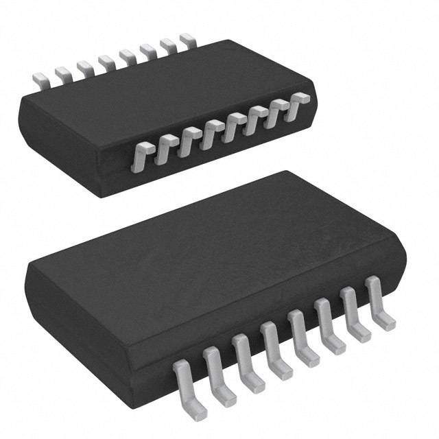
| 描述 | IC DGTL ISO 4CH LOGIC 16SOIC |
| 产品分类 | |
| IsolatedPower | 无 |
| 品牌 | Analog Devices Inc |
| 数据手册 | |
| 产品图片 |
|
| 产品型号 | ADUM2400ARWZ-RL |
| PulseWidthDistortion(Max) | 40ns |
| rohs | 无铅 / 符合限制有害物质指令(RoHS)规范要求 |
| 产品系列 | iCoupler® |
| 上升/下降时间(典型值) | 2.5ns, 2.5ns |
| 传播延迟tpLH/tpHL(最大值) | 100ns, 100ns |
| 供应商器件封装 | 16-SOIC |
| 共模瞬态抗扰度(最小值) | 25kV/µs |
| 其它名称 | ADUM2400ARWZ-RLDKR |
| 其它图纸 |
|
| 包装 | Digi-Reel® |
| 封装/外壳 | 16-SOIC(0.295",7.50mm 宽) |
| 工作温度 | -40°C ~ 105°C |
| 技术 | 磁耦合 |
| 数据速率 | 1Mbps |
| 标准包装 | 1 |
| 电压-电源 | 2.7 V ~ 5.5 V |
| 电压-隔离 | 5000Vrms |
| 类型 | 通用 |
| 脉宽失真(最大) | 40ns |
| 视频文件 | http://www.digikey.cn/classic/video.aspx?PlayerID=1364138032001&width=640&height=505&videoID=2219593469001http://www.digikey.cn/classic/video.aspx?PlayerID=1364138032001&width=640&height=505&videoID=2219593470001http://www.digikey.cn/classic/video.aspx?PlayerID=1364138032001&width=640&height=505&videoID=2219614223001 |
| 输入-输入侧1/输入侧2 | 4/0 |
| 通道数 | 4 |
| 通道类型 | 单向 |
| 隔离式电源 | 无 |


- 商务部:美国ITC正式对集成电路等产品启动337调查
- 曝三星4nm工艺存在良率问题 高通将骁龙8 Gen1或转产台积电
- 太阳诱电将投资9.5亿元在常州建新厂生产MLCC 预计2023年完工
- 英特尔发布欧洲新工厂建设计划 深化IDM 2.0 战略
- 台积电先进制程称霸业界 有大客户加持明年业绩稳了
- 达到5530亿美元!SIA预计今年全球半导体销售额将创下新高
- 英特尔拟将自动驾驶子公司Mobileye上市 估值或超500亿美元
- 三星加码芯片和SET,合并消费电子和移动部门,撤换高东真等 CEO
- 三星电子宣布重大人事变动 还合并消费电子和移动部门
- 海关总署:前11个月进口集成电路产品价值2.52万亿元 增长14.8%


PDF Datasheet 数据手册内容提取
Quad-Channel Digital Isolators Data Sheet ADuM2400/ADuM2401/ADuM2402 FEATURES FUNCTIONAL BLOCK DIAGRAMS Low power operation 5 V operation VDD1 1 ADuM2400 16VDD2 1.0 mA per channel maximum @ 0 Mbps to 2 Mbps GND1 2 15GND2 VIA 3 ENCODE DECODE 14VOA 3.5 mA per channel maximum @ 10 Mbps 31 mA per channel maximum @ 90 Mbps VIB 4 ENCODE DECODE 13VOB 3 V operation VIC 5 ENCODE DECODE 12VOC 0.7 mA per channel maximum @ 0 Mbps to 2 Mbps VID 6 ENCODE DECODE 11VOD 22.01 m mAA p peerr c chhaannnneell m maaxxiimmuumm @ @ 9 100 M Mbbppss GNNDC1 87 190VGEN2D2 05007-001 Figure 1. ADuM2400 Bidirectional communication 3 V/5 V level translation VDD1 1 ADuM2401 16VDD2 High temperature operation: 105°C GND1 2 15GND2 High data rate: dc to 90 Mbps (NRZ) VIA 3 ENCODE DECODE 14VOA Precise timing characteristics VIB 4 ENCODE DECODE 13VOB 2 ns maximum pulse width distortion VIC 5 ENCODE DECODE 12VOC 2 ns maximum channel-to-channel matching VOD 6 DECODE ENCODE 11VID High common-mode transient immunity: >25 kV/μs O16u-tlpeaudt eSnOaIbCl we ifduen cbtoiodny package version (RW-16) GNVDE11 87 190VGEN2D2 05007-002 Figure 2. ADuM2401 16-lead SOIC wide body enhanced creepage version (RI-16) Safety and regulatory approvals (RI-16 package) VDD1 1 ADuM2402 16VDD2 UL recognition: 5000 V rms for 1 minute per UL 1577 GND1 2 15GND2 CSA Component Acceptance Notice 5A VIA 3 ENCODE DECODE 14VOA IEC 60601-1: 250 V rms (reinforced) VIB 4 ENCODE DECODE 13VOB IEC 60950-1: 400 V rms (reinforced) VOC 5 DECODE ENCODE 12VIC VDE Certificate of Conformity VOD 6 DECODE ENCODE 11VID DVIIONRM V = V 8D4E6 V V 0 p8e8a4k- 10 (VDE V 0884-10):2006-12 GNVDE11 87 190VGEN2D2 05007-003 APPLICATIONS Figure 3. ADuM2402 General-purpose, high voltage, multichannel isolation ture and lifetime effects are eliminated with the simple iCoupler Medical equipment digital interfaces and stable performance characteristics. Further- Motor drives more, iCoupler devices run at one-tenth to one-sixth the power Power supplies of optocouplers at comparable signal data rates. GENERAL DESCRIPTION The ADuM2400/ADuM2401/ADuM2402 isolators provide four The ADuM2400/ADuM2401/ADuM24021 are 4-channel digital independent isolation channels in a variety of channel configura- isolators based on Analog Devices, Inc., iCoupler® technology. tions and data rates (see the Ordering Guide). The ADuM2400/ Combining high speed CMOS and monolithic air core transformer ADuM2401/ADuM2402 models operate with the supply voltage technology, these isolation components provide outstanding of either side ranging from 2.7 V to 5.5 V, providing compatibil- performance characteristics that are superior to alternatives, such ity with lower voltage systems as well as enabling a voltage as optocoupler devices. translation functionality across the isolation barrier. In addition, the ADuM2400/ADuM2401/ADuM2402 provide low pulse By avoiding the use of LEDs and photodiodes, iCoupler devices width distortion (<2 ns for CRWZ grade) and tight channel-to- remove the design difficulties commonly associated with opto- channel matching (<2 ns for CRWZ grade). The ADuM2400/ couplers. The typical optocoupler concerns regarding uncertain ADuM2401/ADuM2402 isolators have a patented refresh feature current transfer ratios, nonlinear transfer functions, and tempera that ensures dc correctness in the absence of input logic transitions 1 Protected by U.S. Patents 5,952,849; 6,873,065; and 7,075,329. and during power-up/power-down conditions. Rev. F Document Feedback Information furnished by Analog Devices is believed to be accurate and reliable. However, no responsibility is assumed by Analog Devices for its use, nor for any infringements of patents or other One Technology Way, P.O. Box 9106, Norwood, MA 02062-9106, U.S.A. rights of third parties that may result from its use. Specifications subject to change without notice. No license is granted by implication or otherwise under any patent or patent rights of Analog Devices. Tel: 781.329.4700 ©2005–2015 Analog Devices, Inc. All rights reserved. Trademarks and registered trademarks are the property of their respective owners. Technical Support www.analog.com
ADuM2400/ADuM2401/ADuM2402 Data Sheet TABLE OF CONTENTS Features .............................................................................................. 1 Recommended Operating Conditions .................................... 11 Applications ....................................................................................... 1 Absolute Maximum Ratings ......................................................... 12 General Description ......................................................................... 1 ESD Caution................................................................................ 12 Functional Block Diagrams ............................................................. 1 Pin Configurations and Function Descriptions ......................... 13 Revision History ............................................................................... 2 Typical Performance Characteristics ........................................... 16 Specifications ..................................................................................... 3 Application Information ................................................................ 18 Electrical Characteristics—5 V Operation................................ 3 PC Board Layout ........................................................................ 18 Electrical Characteristics—3 V Operation................................ 5 Propagation Delay-Related Parameters ................................... 18 Electrical Characteristics—Mixed 5 V/3 V or 3 V/5 V DC Correctness and Magnetic Field Immunity.......................... 18 Operation ....................................................................................... 7 Power Consumption .................................................................. 19 Package Characteristics ............................................................. 10 Insulation Lifetime ..................................................................... 20 Regulatory Information ............................................................. 10 Outline Dimensions ....................................................................... 21 Insulation and Safety-Related Specifications .......................... 10 Ordering Guide .......................................................................... 22 DIN V VDE V 0884-10 (VDE V 0884-10) Insulation Characteristics ............................................................................ 11 REVISION HISTORY 7/15—Rev. E to Rev. F 6/07—Rev. A to Rev. B Changes to Table 5 and Table 6 ..................................................... 10 Updated VDE Certification Throughout ....................................... 1 Updated Outline Dimensions ....................................................... 21 Changes to Features and Note 1 ...................................................... 1 Changes to Ordering Guide .......................................................... 22 Changes to Figure 1, Figure 2, and Figure 3 .................................. 1 Changes to Regulatory Information ............................................ 10 2/12—Rev. D to Rev. E Changes to Table 7 .......................................................................... 11 Created Hyperlink for Safety and Regulatory Approvals Changes to Insulation Lifetime Section ...................................... 20 Entry in Features Section ................................................................. 1 Updated Outline Dimensions ....................................................... 21 Change to PC Board Layout Section ............................................ 18 Changes to Ordering Guide .......................................................... 21 8/11—Rev. C to Rev. D 1/06—Rev. 0 to Rev. A Added 16-Lead SOIC_IC .................................................. Universal Changes to Regulatory Information Section .............................. 13 Changes to Features Section and General Description Updated Outline Dimensions ....................................................... 23 Section ................................................................................................ 1 Changes to Ordering Guide .......................................................... 23 Changes to Table 5 and Table 6 ..................................................... 10 Changes to Table 8 Endnote .......................................................... 11 9/05—Revision 0: Initial Version Updated Outline Dimensions ....................................................... 21 Changes to Ordering Guide .......................................................... 21 7/08—Rev. B to Rev. C Changes to Layout ............................................................................ 1 Changes to Table 6 .......................................................................... 10 Rev. F | Page 2 of 24
Data Sheet ADuM2400/ADuM2401/ADuM2402 SPECIFICATIONS ELECTRICAL CHARACTERISTICS—5 V OPERATION1 4.5 V ≤ V ≤ 5.5 V, 4.5 V ≤ V ≤ 5.5 V. All minimum/maximum specifications apply over the entire recommended operation range, DD1 DD2 unless otherwise noted. All typical specifications are at T = 25°C, V = V = 5 V. A DD1 DD2 Table 1. Parameter Symbol Min Typ Max Unit Test Conditions DC SPECIFICATIONS Input Supply Current per Channel, Quiescent I 0.50 0.53 mA DDI (Q) Output Supply Current per Channel, Quiescent I 0.19 0.21 mA DDO (Q) ADuM2400 Total Supply Current, Four Channels2 DC to 2 Mbps V Supply Current I 2.2 2.8 mA DC to 1 MHz logic signal frequency DD1 DD1 (Q) V Supply Current I 0.9 1.4 mA DC to 1 MHz logic signal frequency DD2 DD2 (Q) 10 Mbps (BRWZ and CRWZ Grades Only) V Supply Current I 8.6 10.6 mA 5 MHz logic signal frequency DD1 DD1 (10) V Supply Current I 2.6 3.5 mA 5 MHz logic signal frequency DD2 DD2 (10) 90 Mbps (CRWZ Grade Only) V Supply Current I 70 100 mA 45 MHz logic signal frequency DD1 DD1 (90) V Supply Current I 18 25 mA 45 MHz logic signal frequency DD2 DD2 (90) ADuM2401 Total Supply Current, Four Channels2 DC to 2 Mbps V Supply Current I 1.8 2.4 mA DC to 1 MHz logic signal frequency DD1 DD1 (Q) V Supply Current I 1.2 1.8 mA DC to 1 MHz logic signal frequency DD2 DD2 (Q) 10 Mbps (BRWZ and CRWZ Grades Only) V Supply Current I 7.1 9.0 mA 5 MHz logic signal frequency DD1 DD1 (10) V Supply Current I 4.1 5.0 mA 5 MHz logic signal frequency DD2 DD2 (10) 90 Mbps (CRWZ Grade Only) V Supply Current I 57 82 mA 45 MHz logic signal frequency DD1 DD1 (90) V Supply Current I 31 43 mA 45 MHz logic signal frequency DD2 DD2 (90) ADuM2402 Total Supply Current, Four Channels2 DC to 2 Mbps V or V Supply Current I , I 1.5 2.1 mA DC to 1 MHz logic signal frequency DD1 DD2 DD1 (Q) DD2 (Q) 10 Mbps (BRWZ and CRWZ Grades Only) V or V Supply Current I , I 5.6 7.0 mA 5 MHz logic signal frequency DD1 DD2 DD1 (10) DD2 (10) 90 Mbps (CRWZ Grade Only) V or V Supply Current I , I 44 62 mA 45 MHz logic signal frequency DD1 DD2 DD1 (90) DD2 (90) For All Models Input Currents I , I , I , −10 +0.01 +10 µA 0 V ≤ V , V , V , V ≤ V or V , IA IB IC IA IB IC ID DD1 DD2 I , I , I 0 V ≤ V , V ≤ V or V ID E1 E2 E1 E2 DD1 DD2 Logic High Input Threshold V , V 2.0 V IH EH Logic Low Input Threshold V , V 0.8 V IL EL Logic High Output Voltages V , V , (V or V ) − 0.1 5.0 V I = −20 µA, V = V OAH OBH DD1 DD2 Ox Ix IxH VOCH, VODH (VDD1 or VDD2) − 0.4 4.8 V IOx = −4 mA, VIx = VIxH Logic Low Output Voltages V , V , 0.0 0.1 V I = 20 µA, V = V OAL OBL Ox Ix IxL VOCL, VODL 0.04 0.1 V IOx = 400 µA, VIx = VIxL 0.2 0.4 V I = 4 mA, V = V Ox Ix IxL SWITCHING SPECIFICATIONS ADuM2400ARWZ/ADuM2401ARWZ/ ADuM2402ARWZ Minimum Pulse Width3 PW 1000 ns C = 15 pF, CMOS signal levels L Maximum Data Rate4 1 Mbps C = 15 pF, CMOS signal levels L Propagation Delay5 t , t 50 65 100 ns C = 15 pF, CMOS signal levels PHL PLH L Pulse Width Distortion, |t − t |5 PWD 40 ns C = 15 pF, CMOS signal levels PLH PHL L Propagation Delay Skew6 t 50 ns C = 15 pF, CMOS signal levels PSK L Channel-to-Channel Matching7 t t 50 ns C = 15 pF, CMOS signal levels PSKCD/PSKOD L Rev. F | Page 3 of 24
ADuM2400/ADuM2401/ADuM2402 Data Sheet Parameter Symbol Min Typ Max Unit Test Conditions ADuM2400BRWZ/ADuM2401BRWZ/ ADuM2402BRWZ Minimum Pulse Width3 PW 100 ns C = 15 pF, CMOS signal levels L Maximum Data Rate4 10 Mbps C = 15 pF, CMOS signal levels L Propagation Delay5 t , t 20 32 50 ns C = 15 pF, CMOS signal levels PHL PLH L Pulse Width Distortion, |t − t |5 PWD 3 ns C = 15 pF, CMOS signal levels PLH PHL L Change vs. Temperature 5 ps/°C C = 15 pF, CMOS signal levels L Propagation Delay Skew6 t 15 ns C = 15 pF, CMOS signal levels PSK L Channel-to-Channel Matching, t 3 ns C = 15 pF, CMOS signal levels PSKCD L Codirectional Channels7 Channel-to-Channel Matching, t 6 ns C = 15 pF, CMOS signal levels PSKOD L Opposing-Directional Channels7 ADuM2400CRWZ/ADuM2401CRWZ/ ADuM2402CRWZ Minimum Pulse Width3 PW 8.3 11.1 ns C = 15 pF, CMOS signal levels L Maximum Data Rate4 90 120 Mbps C = 15 pF, CMOS signal levels L Propagation Delay5 t , t 18 27 32 ns C = 15 pF, CMOS signal levels PHL PLH L Pulse Width Distortion, |t − t |5 PWD 0.5 2 ns C = 15 pF, CMOS signal levels PLH PHL L Change vs. Temperature 3 ps/°C C = 15 pF, CMOS signal levels L Propagation Delay Skew6 t 10 ns C = 15 pF, CMOS signal levels PSK L Channel-to-Channel Matching, t 2 ns C = 15 pF, CMOS signal levels PSKCD L Codirectional Channels7 Channel-to-Channel Matching, t 5 ns C = 15 pF, CMOS signal levels PSKOD L Opposing-Directional Channels7 For All Models Output Disable Propagation Delay t , t 6 8 ns C = 15 pF, CMOS signal levels PHZ PLH L (High/Low to High Impedance) Output Enable Propagation Delay t , t 6 8 ns C = 15 pF, CMOS signal levels PZH PZL L (High Impedance to High/Low) Output Rise/Fall Time (10% to 90%) t/t 2.5 ns C = 15 pF, CMOS signal levels R F L Common-Mode Transient Immunity at |CM | 25 35 kV/µs V = V or V , V = 1000 V, H Ix DD1 DD2 CM Logic High Output8 transient magnitude = 800 V Common-Mode Transient Immunity at |CM| 25 35 kV/µs V = 0 V, V = 1000 V, L Ix CM Logic Low Output8 transient magnitude = 800 V Refresh Rate f 1.2 Mbps r Input Dynamic Supply Current per Channel9 I 0.19 mA/Mbps DDI (D) Output Dynamic Supply Current per Channel9 I 0.05 mA/Mbps DDO (D) 1 All voltages are relative to their respective ground. 2 Supply current values are for all four channels combined running at identical data rates. Output supply current values are specified with no output load present. The supply current associated with an individual channel operating at a given data rate can be calculated as described in the Power Consumption section. See Figure 8 through Figure 10 for information on per channel supply current as a function of data rate for unloaded and loaded conditions. See Figure 11 through Figure 15 for total V and V supply currents as a function of data rate for ADuM2400/ADuM2401/ADuM2402 channel configurations. DD1 DD2 3 The minimum pulse width is the shortest pulse width at which the specified pulse width distortion is guaranteed. 4 The maximum data rate is the fastest data rate at which the specified pulse width distortion is guaranteed. 5 t propagation delay is measured from the 50% level of the falling edge of the V signal to the 50% level of the falling edge of the V signal. t propagation delay is PHL Ix Ox PLH measured from the 50% level of the rising edge of the V signal to the 50% level of the rising edge of the V signal. Ix Ox 6 t is the magnitude of the worst-case difference in t or t that is measured between units at the same operating temperature, supply voltages, and output load PSK PHL PLH within the recommended operating conditions. 7 Codirectional channel-to-channel matching is the absolute value of the difference in propagation delays between any two channels with inputs on the same side of the isolation barrier. Opposing directional channel-to-channel matching is the absolute value of the difference in propagation delays between any two channels with inputs on opposing sides of the isolation barrier. 8 CM is the maximum common-mode voltage slew rate that can be sustained while maintaining V > 0.8 V . CM is the maximum common-mode voltage slew rate H O DD2 L that can be sustained while maintaining V < 0.8 V. The common-mode voltage slew rates apply to both rising and falling common-mode voltage edges. The transient O magnitude is the range over which the common mode is slewed. 9 Dynamic supply current is the incremental amount of supply current required for a 1 Mbps increase in signal data rate. See Figure 8 through Figure 10 for information on per channel supply current for unloaded and loaded conditions. See the Power Consumption section for guidance on calculating per channel supply current for a given data rate. Rev. F | Page 4 of 24
Data Sheet ADuM2400/ADuM2401/ADuM2402 ELECTRICAL CHARACTERISTICS—3 V OPERATION1 2.7 V ≤ V ≤ 3.6 V, 2.7 V ≤ V ≤ 3.6 V. All minimum/maximum specifications apply over the entire recommended operation range, DD1 DD2 unless otherwise noted. All typical specifications are at T = 25°C, V = V = 3.0 V. A DD1 DD2 Table 2. Parameter Symbol Min Typ Max Unit Test Conditions DC SPECIFICATIONS Input Supply Current per Channel, Quiescent I 0.26 0.31 mA DDI (Q) Output Supply Current per Channel, Quiescent I 0.11 0.14 mA DDO (Q) ADuM2400 Total Supply Current, Four Channels2 DC to 2 Mbps V Supply Current I 1.2 1.9 mA DC to 1 MHz logic signal frequency DD1 DD1 (Q) V Supply Current I 0.5 0.9 mA DC to 1 MHz logic signal frequency DD2 DD2 (Q) 10 Mbps (BRWZ and CRWZ Grades Only) V Supply Current I 4.5 6.5 mA 5 MHz logic signal frequency DD1 DD1 (10) V Supply Current I 1.4 2.0 mA 5 MHz logic signal frequency DD2 DD2 (10) 90 Mbps (CRWZ Grade Only) V Supply Current I 37 65 mA 45 MHz logic signal frequency DD1 DD1 (90) V Supply Current I 11 15 mA 45 MHz logic signal frequency DD2 DD2 (90) ADuM2401 Total Supply Current, Four Channels2 DC to 2 Mbps V Supply Current I 1.0 1.6 mA DC to 1 MHz logic signal frequency DD1 DD1 (Q) V Supply Current I 0.7 1.2 mA DC to 1 MHz logic signal frequency DD2 DD2 (Q) 10 Mbps (BRWZ and CRWZ Grades Only) V Supply Current I 3.7 5.4 mA 5 MHz logic signal frequency DD1 DD1 (10) V Supply Current I 2.2 3.0 mA 5 MHz logic signal frequency DD2 DD2 (10) 90 Mbps (CRWZ Grade Only) V Supply Current I 30 52 mA 45 MHz logic signal frequency DD1 DD1 (90) V Supply Current I 18 27 mA 45 MHz logic signal frequency DD2 DD2 (90) ADuM2402 Total Supply Current, Four Channels2 DC to 2 Mbps V or V Supply Current I , I 0.9 1.5 mA DC to 1 MHz logic signal frequency DD1 DD2 DD1 (Q) DD2 (Q) 10 Mbps (BRWZ and CRWZ Grades Only) V or V Supply Current I , I 3.0 4.2 mA 5 MHz logic signal frequency DD1 DD2 DD1 (10) DD2 (10) 90 Mbps (CRWZ Grade Only) V or V Supply Current I , I 24 39 mA 45 MHz logic signal frequency DD1 DD2 DD1 (90) DD2 (90) For All Models Input Currents I , I , I , −10 +0.01 +10 µA 0 V ≤ V , V , V , V ≤ V or V , IA IB IC IA IB IC ID DD1 DD2 I , I , I 0 V ≤ V , V ≤ V or V ID E1 E2 E1 E2 DD1 DD2 Logic High Input Threshold V , V 1.6 V IH EH Logic Low Input Threshold V , V 0.4 V IL EL Logic High Output Voltages V , V , (V or V ) − 0.1 3.0 V I = −20 µA, V = V OAH OBH DD1 DD2 Ox Ix IxH VOCH, VODH (VDD1 or VDD2) − 0.4 2.8 V IOx = −4 mA, VIx = VIxH Logic Low Output Voltages V , V , 0.0 0.1 V I = 20 µA, V = V OAL OBL Ox Ix IxL VOCL, VODL 0.04 0.1 V IOx = 400 µA, VIx = VIxL 0.2 0.4 V I = 4 mA, V = V Ox Ix IxL SWITCHING SPECIFICATIONS ADuM2400ARWZ/ADuM2401ARWZ/ ADuM2402ARWZ Minimum Pulse Width3 PW 1000 ns C = 15 pF, CMOS signal levels L Maximum Data Rate4 1 Mbps C = 15 pF, CMOS signal levels L Propagation Delay5 t , t 50 75 100 ns C = 15 pF, CMOS signal levels PHL PLH L Pulse Width Distortion, |t − t |5 PWD 40 ns C = 15 pF, CMOS signal levels PLH PHL L Propagation Delay Skew6 t 50 ns C = 15 pF, CMOS signal levels PSK L Channel-to-Channel Matching7 t t 50 ns C = 15 pF, CMOS signal levels PSKCD/PSKOD L Rev. F | Page 5 of 24
ADuM2400/ADuM2401/ADuM2402 Data Sheet Parameter Symbol Min Typ Max Unit Test Conditions ADuM2400BRWZ/ADuM2401BRWZ/ ADuM2402BRWZ Minimum Pulse Width3 PW 100 ns C = 15 pF, CMOS signal levels L Maximum Data Rate4 10 Mbps C = 15 pF, CMOS signal levels L Propagation Delay5 t , t 20 38 50 ns C = 15 pF, CMOS signal levels PHL PLH L Pulse Width Distortion, |t − t |5 PWD 3 ns C = 15 pF, CMOS signal levels PLH PHL L Change vs. Temperature 5 ps/°C C = 15 pF, CMOS signal levels L Propagation Delay Skew6 t 22 ns C = 15 pF, CMOS signal levels PSK L Channel-to-Channel Matching, t 3 ns C = 15 pF, CMOS signal levels PSKCD L Codirectional Channels7 Channel-to-Channel Matching, t 6 ns C = 15 pF, CMOS signal levels PSKOD L Opposing-Directional Channels7 ADuM2400CRWZ/ADuM2401CRWZ/ ADuM2402CRWZ Minimum Pulse Width3 PW 8.3 11.1 ns C = 15 pF, CMOS signal levels L Maximum Data Rate4 90 120 Mbps C = 15 pF, CMOS signal levels L Propagation Delay5 t , t 20 34 45 ns C = 15 pF, CMOS signal levels PHL PLH L Pulse Width Distortion, |t − t |5 PWD 0.5 2 ns C = 15 pF, CMOS signal levels PLH PHL L Change vs. Temperature 3 ps/°C C = 15 pF, CMOS signal levels L Propagation Delay Skew6 t 16 ns C = 15 pF, CMOS signal levels PSK L Channel-to-Channel Matching, t 2 ns C = 15 pF, CMOS signal levels PSKCD L Codirectional Channels7 Channel-to-Channel Matching, t 5 ns C = 15 pF, CMOS signal levels PSKOD L Opposing-Directional Channels7 For All Models Output Disable Propagation Delay t , t 6 8 ns C = 15 pF, CMOS signal levels PHZ PLH L (High/Low to High Impedance) Output Enable Propagation Delay t , t 6 8 ns C = 15 pF, CMOS signal levels PZH PZL L (High Impedance to High/Low) Output Rise/Fall Time (10% to 90%) t/t 3 ns C = 15 pF, CMOS signal levels R F L Common-Mode Transient Immunity at |CM | 25 35 kV/µs V = V or V , V = 1000 V, H Ix DD1 DD2 CM Logic High Output8 transient magnitude = 800 V Common-Mode Transient Immunity at |CM| 25 35 kV/µs V = 0 V, V = 1000 V, L Ix CM Logic Low Output8 transient magnitude = 800 V Refresh Rate f 1.1 Mbps r Input Dynamic Supply Current per Channel9 I 0.10 mA/Mbps DDI (D) Output Dynamic Supply Current per Channel9 I 0.03 mA/Mbps DDO (D) 1 All voltages are relative to their respective ground. 2 Supply current values are for all four channels combined running at identical data rates. Output supply current values are specified with no output load present. The supply current associated with an individual channel operating at a given data rate can be calculated as described in the Power Consumption section. See Figure 8 through Figure 10 for information on per channel supply current as a function of data rate for unloaded and loaded conditions. See Figure 11 through Figure 15 for total V and V supply currents as a function of data rate for ADuM2400/ADuM2401/ADuM2402 channel configurations. DD1 DD2 3 The minimum pulse width is the shortest pulse width at which the specified pulse width distortion is guaranteed. 4 The maximum data rate is the fastest data rate at which the specified pulse width distortion is guaranteed. 5 t propagation delay is measured from the 50% level of the falling edge of the V signal to the 50% level of the falling edge of the V signal. t propagation delay is PHL Ix Ox PLH measured from the 50% level of the rising edge of the V signal to the 50% level of the rising edge of the V signal. Ix Ox 6 t is the magnitude of the worst-case difference in t or t that is measured between units at the same operating temperature, supply voltages, and output load PSK PHL PLH within the recommended operating conditions. 7 Codirectional channel-to-channel matching is the absolute value of the difference in propagation delays between any two channels with inputs on the same side of the isolation barrier. Opposing directional channel-to-channel matching is the absolute value of the difference in propagation delays between any two channels with inputs on opposing sides of the isolation barrier. 8 CM is the maximum common-mode voltage slew rate that can be sustained while maintaining V > 0.8 V . CM is the maximum common-mode voltage slew rate H O DD2 L that can be sustained while maintaining V < 0.8 V. The common-mode voltage slew rates apply to both rising and falling common-mode voltage edges. The transient O magnitude is the range over which the common mode is slewed. 9 Dynamic supply current is the incremental amount of supply current required for a 1 Mbps increase in signal data rate. See Figure 8 through Figure 10 for information on per channel supply current for unloaded and loaded conditions. See the Power Consumption section for guidance on calculating per channel supply current for a given data rate. Rev. F | Page 6 of 24
Data Sheet ADuM2400/ADuM2401/ADuM2402 ELECTRICAL CHARACTERISTICS—MIXED 5 V/3 V OR 3 V/5 V OPERATION1 5 V/3 V operation: 4.5 V ≤ V ≤ 5.5 V, 2.7 V ≤ V ≤ 3.6 V. 3 V/5 V operation: 2.7 V ≤ V ≤ 3.6 V, 4.5 V ≤ V ≤ 5.5 V. All DD1 DD2 DD1 DD2 minimum/maximum specifications apply over the entire recommended operation range, unless otherwise noted. All typical specifications are at T = 25°C; V = 3.0 V, V = 5 V; or V = 5 V, V = 3.0 V. A DD1 DD2 DD1 DD2 Table 3. Parameter Symbol Min Typ Max Unit Test Conditions DC SPECIFICATIONS Input Supply Current per Channel, Quiescent I DDI (Q) 5 V/3 V Operation 0.50 0.53 mA 3 V/5 V Operation 0.26 0.31 mA Output Supply Current per Channel, Quiescent I DDO (Q) 5 V/3 V Operation 0.11 0.14 mA 3 V/5 V Operation 0.19 0.21 mA ADuM2400 Total Supply Current, Four Channels2 DC to 2 Mbps V Supply Current I DD1 DD1 (Q) 5 V/3 V Operation 2.2 2.8 mA DC to 1 MHz logic signal frequency 3 V/5 V Operation 1.2 1.9 mA DC to 1 MHz logic signal frequency V Supply Current I DD2 DD2 (Q) 5 V/3 V Operation 0.5 0.9 mA DC to 1 MHz logic signal frequency 3 V/5 V Operation 0.9 1.4 mA DC to 1 MHz logic signal frequency 10 Mbps (BRWZ and CRWZ Grades Only) V Supply Current I DD1 DD1 (10) 5 V/3 V Operation 8.6 10.6 mA 5 MHz logic signal frequency 3 V/5 V Operation 4.5 6.5 mA 5 MHz logic signal frequency V Supply Current I DD2 DD2 (10) 5 V/3 V Operation 1.4 2.0 mA 5 MHz logic signal frequency 3 V/5 V Operation 2.6 3.5 mA 5 MHz logic signal frequency 90 Mbps (CRWZ Grade Only) V Supply Current I DD1 DD1 (90) 5 V/3 V Operation 70 100 mA 45 MHz logic signal frequency 3 V/5 V Operation 37 65 mA 45 MHz logic signal frequency V Supply Current I DD2 DD2 (90) 5 V/3 V Operation 11 15 mA 45 MHz logic signal frequency 3 V/5 V Operation 18 25 mA 45 MHz logic signal frequency ADuM2401 Total Supply Current, Four Channels2 DC to 2 Mbps V Supply Current I DD1 DD1 (Q) 5 V/3 V Operation 1.8 2.4 mA DC to 1 MHz logic signal frequency 3 V/5 V Operation 1.0 1.6 mA DC to 1 MHz logic signal frequency V Supply Current I DD2 DD2 (Q) 5 V/3 V Operation 0.7 1.2 mA DC to 1 MHz logic signal frequency 3 V/5 V Operation 1.2 1.8 mA DC to 1 MHz logic signal frequency 10 Mbps (BRWZ and CRWZ Grades Only) V Supply Current I DD1 DD1 (10) 5 V/3 V Operation 7.1 9.0 mA 5 MHz logic signal frequency 3 V/5 V Operation 3.7 5.4 mA 5 MHz logic signal frequency V Supply Current I DD2 DD2 (10) 5 V/3 V Operation 2.2 3.0 mA 5 MHz logic signal frequency 3 V/5 V Operation 4.1 5.0 mA 5 MHz logic signal frequency 90 Mbps (CRWZ Grade Only) V Supply Current I DD1 DD1 (90) 5 V/3 V Operation 57 82 mA 45 MHz logic signal frequency 3 V/5 V Operation 30 52 mA 45 MHz logic signal frequency Rev. F | Page 7 of 24
ADuM2400/ADuM2401/ADuM2402 Data Sheet Parameter Symbol Min Typ Max Unit Test Conditions V Supply Current I DD2 DD2 (90) 5 V/3 V Operation 18 27 mA 45 MHz logic signal frequency 3 V/5 V Operation 31 43 mA 45 MHz logic signal frequency ADuM2402 Total Supply Current, Four Channels2 DC to 2 Mbps V Supply Current I DD1 DD1 (Q) 5 V/3 V Operation 1.5 2.1 mA DC to 1 MHz logic signal frequency 3 V/5 V Operation 0.9 1.5 mA DC to 1 MHz logic signal frequency V Supply Current I DD2 DD2 (Q) 5 V/3 V Operation 0.9 1.5 mA DC to 1 MHz logic signal frequency 3 V/5 V Operation 1.5 2.1 mA DC to 1 MHz logic signal frequency 10 Mbps (BRWZ and CRWZ Grades Only) V Supply Current I DD1 DD1 (10) 5 V/3 V Operation 5.6 7.0 mA 5 MHz logic signal frequency 3 V/5 V Operation 3.0 4.2 mA 5 MHz logic signal frequency V Supply Current I DD2 DD2 (10) 5 V/3 V Operation 3.0 4.2 mA 5 MHz logic signal frequency 3 V/5 V Operation 5.6 7.0 mA 5 MHz logic signal frequency 90 Mbps (CRWZ Grade Only) V Supply Current I DD1 DD1 (90) 5 V/3 V Operation 44 62 mA 45 MHz logic signal frequency 3 V/5 V Operation 24 39 mA 45 MHz logic signal frequency V Supply Current I DD2 DD2 (90) 5 V/3 V Operation 24 39 mA 45 MHz logic signal frequency 3 V/5 V Operation 44 62 mA 45 MHz logic signal frequency For All Models Input Currents I , I , I , −10 +0.01 +10 µA 0 V ≤ V , V , V , V ≤ V or V , IA IB IC IA IB IC ID DD1 DD2 I , I , I 0 V ≤ V , V ≤ V or V ID E1 E2 E1 E2 DD1 DD2 Logic High Input Threshold V , V IH EH 5 V/3 V Operation 2.0 V 3 V/5 V Operation 1.6 V Logic Low Input Threshold V , V IL EL 5 V/3 V Operation 0.8 V 3 V/5 V Operation 0.4 V Logic High Output Voltages V , V , (V or V ) − (V or V ) V I = −20 µA, V = V OAH OBH DD1 DD2 DD1 DD2 Ox Ix IxH V , V 0.1 OCH ODH (V or V ) − (V or V ) − V I = −4 mA, V = V DD1 DD2 DD1 DD2 Ox Ix IxH 0.4 0.2 Logic Low Output Voltages V V , 0.0 0.1 V I = 20 µA, V = V OAL, OBL Ox Ix IxL VOCL, VODL 0.04 0.1 V IOx = 400 µA, VIx = VIxL 0.2 0.4 V I = 4 mA, V = V Ox Ix IxL SWITCHING SPECIFICATIONS ADuM2400ARWZ/ADuM2401ARWZ/ ADuM2402ARWZ Minimum Pulse Width3 PW 1000 ns C = 15 pF, CMOS signal levels L Maximum Data Rate4 1 Mbps C = 15 pF, CMOS signal levels L Propagation Delay5 t , t 50 70 100 ns C = 15 pF, CMOS signal levels PHL PLH L Pulse-Width Distortion, |t − t |5 PWD 40 ns C = 15 pF, CMOS signal levels PLH PHL L Propagation Delay Skew6 t 50 ns C = 15 pF, CMOS signal levels PSK L Channel-to-Channel Matching7 t t 50 ns C = 15 pF, CMOS signal levels PSKCD/PSKOD L ADuM2400BRWZ/ADuM2401BRWZ/ ADuM2402BRWZ Minimum Pulse Width3 PW 100 ns C = 15 pF, CMOS signal levels L Maximum Data Rate4 10 Mbps C = 15 pF, CMOS signal levels L Propagation Delay5 t , t 15 35 50 ns C = 15 pF, CMOS signal levels PHL PLH L Rev. F | Page 8 of 24
Data Sheet ADuM2400/ADuM2401/ADuM2402 Parameter Symbol Min Typ Max Unit Test Conditions Pulse Width Distortion, |t − t |5 PWD 3 ns C = 15 pF, CMOS signal levels PLH PHL L Change vs. Temperature 5 ps/°C C = 15 pF, CMOS signal levels L Propagation Delay Skew6 t 22 ns C = 15 pF, CMOS signal levels PSK L Channel-to-Channel Matching, t 3 ns C = 15 pF, CMOS signal levels PSKCD L Codirectional Channels7 Channel-to-Channel Matching, t 6 ns C = 15 pF, CMOS signal levels PSKOD L Opposing-Directional Channels7 ADuM2400CRWZ/ADuM2401CRWZ/ ADuM2402CRWZ Minimum Pulse Width3 PW 8.3 11.1 ns C = 15 pF, CMOS signal levels L Maximum Data Rate4 90 120 Mbps C = 15 pF, CMOS signal levels L Propagation Delay5 t , t 20 30 40 ns C = 15 pF, CMOS signal levels PHL PLH L Pulse Width Distortion, |t − t |5 PWD 0.5 2 ns C = 15 pF, CMOS signal levels PLH PHL L Change vs. Temperature 3 ps/°C C = 15 pF, CMOS signal levels L Propagation Delay Skew6 t 14 ns C = 15 pF, CMOS signal levels PSK L Channel-to-Channel Matching, t 2 ns C = 15 pF, CMOS signal levels PSKCD L Codirectional Channels7 Channel-to-Channel Matching, t 5 ns C = 15 pF, CMOS signal levels PSKOD L Opposing-Directional Channels7 For All Models Output Disable Propagation Delay t , t 6 8 ns C = 15 pF, CMOS signal levels PHZ PLH L (High/Low to High Impedance) Output Enable Propagation Delay t , t 6 8 ns C = 15 pF, CMOS signal levels PZH PZL L (High Impedance to High/Low) Output Rise/Fall Time (10% to 90%) t/t C = 15 pF, CMOS signal levels R F L 5 V/3 V Operation 3.0 ns 3 V/5 V Operation 2.5 ns Common-Mode Transient Immunity at |CM | 25 35 kV/µs V = V or V , V = 1000 V, H Ix DD1 DD2 CM Logic High Output8 transient magnitude = 800 V Common-Mode Transient Immunity at |CM| 25 35 kV/µs V = 0 V, V = 1000 V, L Ix CM Logic Low Output8 transient magnitude = 800 V Refresh Rate f r 5 V/3 V Operation 1.2 Mbps 3 V/5 V Operation 1.1 Mbps Input Dynamic Supply Current per Channel9 I DDI (D) 5 V/3 V Operation 0.19 mA/Mbps 3 V/5 V Operation 0.10 mA/Mbps Output Dynamic Supply Current per Channel9 I DDO (D) 5 V/3 V Operation 0.03 mA/Mbps 3 V/5 V Operation 0.05 mA/Mbps 1 All voltages are relative to their respective ground. 2 Supply current values are for all four channels combined running at identical data rates. Output supply current values are specified with no output load present. The supply current associated with an individual channel operating at a given data rate can be calculated as described in the Power Consumption section. See Figure 8 through Figure 10 for information on per channel supply current as a function of data rate for unloaded and loaded conditions. See Figure 11 through Figure 15 for total V and V supply currents as a function of data rate for ADuM2400/ADuM2401/ADuM2402 channel configurations. DD1 DD2 3 The minimum pulse width is the shortest pulse width at which the specified pulse width distortion is guaranteed. 4 The maximum data rate is the fastest data rate at which the specified pulse width distortion is guaranteed. 5 t propagation delay is measured from the 50% level of the falling edge of the V signal to the 50% level of the falling edge of the V signal. t propagation delay is PHL Ix Ox PLH measured from the 50% level of the rising edge of the V signal to the 50% level of the rising edge of the V signal. Ix Ox 6 t is the magnitude of the worst-case difference in t or t that is measured between units at the same operating temperature, supply voltages, and output load PSK PHL PLH within the recommended operating conditions. 7 Codirectional channel-to-channel matching is the absolute value of the difference in propagation delays between any two channels with inputs on the same side of the isolation barrier. Opposing directional channel-to-channel matching is the absolute value of the difference in propagation delays between any two channels with inputs on opposing sides of the isolation barrier. 8 CM is the maximum common-mode voltage slew rate that can be sustained while maintaining V > 0.8 V . CM is the maximum common-mode voltage slew rate H O DD2 L that can be sustained while maintaining V < 0.8 V. The common-mode voltage slew rates apply to both rising and falling common-mode voltage edges. The transient O magnitude is the range over which the common mode is slewed. 9 Dynamic supply current is the incremental amount of supply current required for a 1 Mbps increase in signal data rate. See Figure 8 through Figure 10 for information on per channel supply current for unloaded and loaded conditions. See the Power Consumption section for guidance on calculating per channel supply current for a given data rate. Rev. F | Page 9 of 24
ADuM2400/ADuM2401/ADuM2402 Data Sheet PACKAGE CHARACTERISTICS Table 4. Parameter Symbol Min Typ Max Unit Test Conditions Resistance (Input to Output)1 R 1012 Ω I-O Capacitance (Input to Output)1 C 2.2 pF f = 1 MHz I-O Input Capacitance2 C 4.0 pF I IC Junction-to-Case Thermal Resistance, Side 1 θ 33 °C/W Thermocouple located at center JCI IC Junction-to-Case Thermal Resistance, Side 2 θ 28 °C/W of package underside JCO 1 Device considered a 2-terminal device: Pin 1, Pin 2, Pin 3, Pin 4, Pin 5, Pin 6, Pin 7, and Pin 8 shorted together and Pin 9, Pin 10, Pin 11, Pin 12, Pin 13, Pin 14, Pin 15, and Pin 16 shorted together. 2 Input capacitance is from any input data pin to ground. REGULATORY INFORMATION The ADuM2400/ADuM2401/ADuM2402 are approved by the organizations listed in Table 5. Refer to Table 10 and the Insulation Lifetime section for details regarding recommended maximum working voltages for specific cross-isolation waveforms and insulation levels. Table 5. UL CSA CQC VDE Recognized Under UL 1577 Approved under CSA Component Acceptance Approved under CQC11-471543-2012 Certified according to Component Recognition Notice 5A DIN V VDE V 0884-10 Program1 (VDE V 0884-10): 2006-122 Single Protection 5000 V rms Basic insulation per CSA 60950-1-07 and Basic insulation per GB4943.1-2011, Reinforced insulation, Isolation Voltage IEC 60950-1, 600 V rms (848 V peak) maximum 600 V rms(848 V peak) maximum 846 V peak working voltage working voltage, tropical climate, altitude ≤ 5000 m RW-16 package: reinforced insulation per RW-16 package: reinforced insulation CSA 60950-1-07 and IEC 60950-1, 380 V rms per GB4943.1-2011, 380 V rms (537 V peak) maximum working voltage; (537 V peak) maximum working reinforced insulation per IEC 60601-1 voltage, tropical climate, altitude ≤ 125 V rms (176 V peak) maximum working 5000 m voltage RI-16 package: reinforced insulation per RI-16 package: reinforced insulation CSA 60950-1-07 and IEC 60950-1, 400 V rms per 400 V rms (565 V peak) maximum (565 V peak) maximum working voltage; working voltage, tropical climate, reinforced insulation per IEC 60601-1 250 V rms altitude ≤ 5000 m (353 V peak) maximum working voltage File E214100 File 205078 File: CQC14001108690 File 2471900-4880-0001 1 In accordance with UL 1577, each ADuM2400/ADuM2401/ADuM2402 is proof tested by applying an insulation test voltage ≥ 6000 V rms for 1 sec (current leakage detection limit = 10 µA). 2 In accordance with DIN V VDE V 0884-10, each ADuM2400/ADuM2401/ADuM2402 is proof tested by applying an insulation test voltage ≥1590 V peak for 1 sec (partial discharge detection limit = 5 pC). The * marking branded on the component designates DIN V VDE V 0884-10 approval. INSULATION AND SAFETY-RELATED SPECIFICATIONS Table 6. Parameter Symbol Value Unit Conditions Rated Dielectric Insulation Voltage 5000 V rms 1-minute duration Minimum External Air Gap L(I01) 8.0 min mm Distance measured from input terminals to output terminals, shortest distance through air along the PCB mounting plane, as an aid to PC board layout Minimum External Tracking (Creepage) RW-16 L(I02) 7.7 min mm Measured from input terminals to output terminals, shortest distance Package path along body Minimum External Tracking (Creepage) RI-16 L(I02) 8.3 min mm Measured from input terminals to output terminals, shortest distance Package path along body Minimum Internal Gap (Internal Clearance) 0.017 min mm Insulation distance through insulation Tracking Resistance (Comparative Tracking CTI >400 V DIN IEC 112/VDE 0303 Part 1 Index) Isolation Group II Material Group (DIN VDE 0110, 1/89, Table 1) Rev. F | Page 10 of 24
Data Sheet ADuM2400/ADuM2401/ADuM2402 DIN V VDE V 0884-10 (VDE V 0884-10) INSULATION CHARACTERISTICS These isolators are suitable for reinforced electrical isolation only within the safety limit data. Maintenance of the safety data is ensured by means of protective circuits. Note that the * marking on packages denotes DIN V VDE V 0884-10 approval for 846 V peak working voltage. Table 7. Description Conditions Symbol Characteristic Unit Installation Classification per DIN VDE 0110 For Rated Mains Voltage ≤ 300 V rms I to IV For Rated Mains Voltage ≤ 450 V rms I to II For Rated Mains Voltage ≤ 600 V rms I to II Climatic Classification 40/105/21 Pollution Degree (DIN VDE 0110, Table 1) 2 Maximum Working Insulation Voltage V 846 V peak IORM Input-to-Output Test Voltage, Method b1 V × 1.875 = V , 100% production test, t = 1 sec, V 1590 V peak IORM PR m PR partial discharge < 5 pC Input-to-Output Test Voltage, Method a V PR After Environmental Tests Subgroup 1 V × 1.6 = V , t = 60 sec, partial discharge < 5 pC 1375 V peak IORM PR m After Input and/or Safety Test Subgroup 2 V × 1.2 = V , t = 60 sec, partial discharge < 5 pC 1018 V peak IORM PR m and Subgroup 3 Highest Allowable Overvoltage Transient overvoltage, t = 10 seconds V 6000 V peak TR TR Safety-Limiting Values Maximum value allowed in the event of a failure; see Figure 4 Case Temperature T 150 °C S Side 1 Current I 265 mA S1 Side 2 Current I 335 mA S2 Insulation Resistance at T V = 500 V R >109 Ω S IO S 350 RECOMMENDED OPERATING CONDITIONS 300 Table 8. A) m Parameter Rating T ( 250 REN SIDE #2 Operating Temperature (TA) −40°C to +105°C UR 200 Supply Voltages1 (VDD1, VDD2) 2.7 V to 5.5 V C G Input Signal Rise and Fall Times 1.0 ms N TI 150 LIMI SIDE #1 1 All voltages are relative to their respective ground. Y- 100 T E F A S 500 05007-004 0 50 100 150 200 CASE TEMPERATURE (°C) Figure 4. Thermal Derating Curve, Dependence of Safety-Limiting Values with Case Temperature per DIN V VDE V 0884-10 Rev. F | Page 11 of 24
ADuM2400/ADuM2401/ADuM2402 Data Sheet ABSOLUTE MAXIMUM RATINGS Table 9. Stresses at or above those listed under Absolute Maximum Parameter Rating Ratings may cause permanent damage to the product. This is a Storage Temperature Range (T ) −65°C to +150°C stress rating only; functional operation of the product at these ST Ambient Operating Temperature −40°C to +105°C or any other conditions above those indicated in the operational Range (T ) section of this specification is not implied. Operation beyond A Supply Voltage Range (V , V )1 −0.5 V to +7.0 V the maximum operating conditions for extended periods may DD1 DD2 Input Voltage Range −0.5 V to V + 0.5 V affect product reliability. DDI (V , V , V , V , V , V )1, 2 IA IB IC ID E1 E2 Output Voltage Range −0.5 V to V + 0.5 V DDO (V , V , V , V )1, 2 ESD CAUTION OA OB OC OD Average Output Current Per Pin3 Side 1 (I ) −18 mA to +18 mA O1 Side 2 (I ) −22 mA to +22 mA O2 Common-Mode Transients4 −100 kV/µs to +100 kV/µs 1 All voltages are relative to their respective ground. 2 V and V refer to the supply voltages on the input and output sides of a DDI DDO given channel, respectively. See the PC Board Layout section. 3 See Figure 4 for maximum rated current values for various temperatures. 4 Refers to common-mode transients across the insulation barrier. Common- mode transients exceeding the Absolute Maximum Rating can cause latch- up or permanent damage. Table 10. Maximum Continuous Working Voltage1 Parameter Max Unit Constraint AC Voltage, Bipolar Waveform 565 V peak 50-year minimum lifetime AC Voltage, Unipolar Waveform Reinforced Insulation 846 V peak Maximum approved working voltage per IEC 60950-1 and VDE V 0884-10 DC Voltage Reinforced Insulation 846 V peak Maximum approved working voltage per IEC 60950-1 and VDE V 0884-10 1 Refers to continuous voltage magnitude imposed across the isolation barrier. See the Insulation Lifetime section for more details. Table 11. Truth Table (Positive Logic) V Input1 V Input V State1 V State1 V Output1 Notes Ix Ex DDI DDO Ox H H or NC Powered Powered H L H or NC Powered Powered L X L Powered Powered Z X H or NC Unpowered Powered H Outputs return to input state within 1 µs of V power restoration. DDI X L Unpowered Powered Z X X Powered Unpowered Indeterminate Outputs return to input state within 1 µs of V power restoration if DDO V state is H or NC. Outputs return to high impedance state within Ex 8 ns of V power restoration if V state is L. DDO Ex 1 V and V refer to the input and output signals of a given channel (A, B, C, or D). V refers to the output enable signal on the same side as the V outputs. V and Ix Ox Ex Ox DDI V refer to the supply voltages on the input and output sides of the given channel, respectively. DDO Rev. F | Page 12 of 24
Data Sheet ADuM2400/ADuM2401/ADuM2402 PIN CONFIGURATIONS AND FUNCTION DESCRIPTIONS VDD1 1 16 VDD2 *GND1 2 15 GND2* VIA 3 ADuM2400 14 VOA VIB 4 TOP VIEW 13 VOB VIC 5 (Not to Scale) 12 VOC VID 6 11 VOD NC 7 10 VE2 *GND1 8NC = NO CONNECT9 GND2* 05007-005 *PIN 2 AND PIN 8 ARE INTERNALLY CONNECTED, AND CONNECTING BOTH TO GND1 IS RECOMMENDED. PIN 9 AND PIN 15 ARE INTERNALLY CONNECTED, AND CONNECTING BOTH TO GND2 IS RECOMMENDED. Figure 5. ADuM2400 Pin Configuration Table 12. ADuM2400 Pin Function Descriptions Pin No. Mnemonic Description 1 V Supply Voltage for Isolator Side 1, 2.7 V to 5.5 V. DD1 2 GND Ground 1. Ground reference for Isolator Side 1. 1 3 V Logic Input A. IA 4 V Logic Input B. IB 5 V Logic Input C. IC 6 V Logic Input D. ID 7 NC No Connect. 8 GND Ground 1. Ground reference for Isolator Side 1. 1 9 GND Ground 2. Ground reference for Isolator Side 2. 2 10 V Output Enable 2. Active high logic input. V , V , V , and V outputs are enabled when V is high or disconnected. E2 OA OB OC OD E2 V , V , V , and V outputs are disabled when V is low. In noisy environments, connecting V to an external logic OA OB OC OD E2 E2 high or low is recommended. 11 V Logic Output D. OD 12 V Logic Output C. OC 13 V Logic Output B. OB 14 V Logic Output A. OA 15 GND Ground 2. Ground reference for Isolator Side 2. 2 16 V Supply Voltage for Isolator Side 2, 2.7 V to 5.5 V. DD2 Rev. F | Page 13 of 24
ADuM2400/ADuM2401/ADuM2402 Data Sheet VDD1 1 16 VDD2 *GND1 2 15 GND2* VIA 3 ADuM2401 14 VOA VIB 4 TOP VIEW 13 VOB VIC 5 (Not to Scale) 12 VOC VOD 6 11 VID VE1 7 10 VE2 *GND1 8 9 GND2* 05007-006 *PIN 2 AND PIN 8 ARE INTERNALLY CONNECTED, AND CONNECTING BOTH TO GND1 IS RECOMMENDED. PIN 9 AND PIN 15 ARE INTERNALLY CONNECTED, AND CONNECTING BOTH TO GND2 IS RECOMMENDED. Figure 6. ADuM2401 Pin Configuration Table 13. ADuM2401 Pin Function Descriptions Pin No. Mnemonic Description 1 V Supply Voltage for Isolator Side 1, 2.7 V to 5.5 V. DD1 2 GND Ground 1. Ground reference for Isolator Side 1. 1 3 V Logic Input A. IA 4 V Logic Input B. IB 5 V Logic Input C. IC 6 V Logic Output D. OD 7 V Output Enable 1. Active high logic input. V output is enabled when V is high or disconnected. V is disabled E1 OD E1 OD when V is low. In noisy environments, connecting V to an external logic high or low is recommended. E1 E1 8 GND Ground 1. Ground reference for Isolator Side 1. 1 9 GND Ground 2. Ground reference for Isolator Side 2. 2 10 V Output Enable 2. Active high logic input. V , V , and V outputs are enabled when V is high or disconnected. V , E2 OA OB OC E2 OA V , and V outputs are disabled when V is low. In noisy environments, connecting V to an external logic high or OB OC E2 E2 low is recommended. 11 V Logic Input D. ID 12 V Logic Output C. OC 13 V Logic Output B. OB 14 V Logic Output A. OA 15 GND Ground 2. Ground reference for Isolator Side 2. 2 16 V Supply Voltage for Isolator Side 2, 2.7 V to 5.5 V. DD2 Rev. F | Page 14 of 24
Data Sheet ADuM2400/ADuM2401/ADuM2402 VDD1 1 16 VDD2 *GND1 2 15 GND2* VIA 3 ADuM2402 14 VOA VIB 4 TOP VIEW 13 VOB VOC 5 (Not to Scale) 12 VIC VOD 6 11 VID VE1 7 10 VE2 *GND1 8 9 GND2* 05007-007 *PIN 2 AND PIN 8 ARE INTERNALLY CONNECTED, AND CONNECTING BOTH TO GND1 IS RECOMMENDED. PIN 9 AND PIN 15 ARE INTERNALLY CONNECTED, AND CONNECTING BOTH TO GND2 IS RECOMMENDED. Figure 7. ADuM2402 Pin Configuration Table 14. ADuM2402 Pin Function Descriptions Pin No. Mnemonic Description 1 V Supply Voltage for Isolator Side 1, 2.7 V to 5.5 V. DD1 2 GND Ground 1. Ground reference for Isolator Side 1. 1 3 V Logic Input A. IA 4 V Logic Input B. IB 5 V Logic Output C. OC 6 V Logic Output D. OD 7 V Output Enable 1. Active high logic input. V and V outputs are enabled when V is high or disconnected. E1 OC OD E1 V and V outputs are disabled when V is low. In noisy environments, connecting V to an external logic high or OC OD E1 E1 low is recommended. 8 GND Ground 1. Ground reference for Isolator Side 1. 1 9 GND Ground 2. Ground reference for Isolator Side 2. 2 10 V Output Enable 2. Active high logic input. V and V outputs are enabled when V is high or disconnected. E2 OA OB E2 V and V outputs are disabled when V is low. In noisy environments, connecting V to an external logic high or OA OB E2 E2 low is recommended. 11 V Logic Input D. ID 12 V Logic Input C. IC 13 V Logic Output B. OB 14 V Logic Output A. OA 15 GND Ground 2. Ground reference for Isolator Side 2. 2 16 V Supply Voltage for Isolator Side 2, 2.7 V to 5.5 V. DD2 Rev. F | Page 15 of 24
ADuM2400/ADuM2401/ADuM2402 Data Sheet TYPICAL PERFORMANCE CHARACTERISTICS 20 80 70 15 60 A) m EL ( A) 50 N m AN 10 T ( 40 H N NT/C 5V URRE 30 5V RE C R 3V 3V U 5 20 C 10 00 20 DA4T0A RATE (M6b0ps) 80 100 05007-008 00 20 DA4T0A RATE (M6b0ps) 80 100 05007-011 Figure 8. Typical Input Supply Current per Channel vs. Data Rate Figure 11. Typical ADuM2400 VDD1 Supply Current vs. Data Rate for 5 V and 3 V Operation (No Output Load) for 5 V and 3 V Operation 6 25 5 20 A) m 4 NEL ( mA) 15 T/CHAN 3 5V RRENT ( 10 N U E 2 C 5V R R U 3V 3V C 5 1 00 20 DA4T0A RATE (M6b0ps) 80 100 05007-009 00 20 DA4T0A RATE (Mb60ps) 80 10005007-012 Figure 9. Typical Output Supply Current per Channel vs. Data Rate Figure 12. Typical ADuM2400 VDD2 Supply Current vs. Data Rate for 5 V and 3 V Operation (No Output Load) for 5 V and 3 V Operation 10 35 30 8 A) 25 m NEL ( 6 mA) 20 AN T ( H N RENT/C 4 5V CURRE 15 5V R 10 CU 3V 2 3V 5 00 20 DA4T0A RATE (M6b0ps) 80 100 05007-010 00 20 DA4T0A RATE (M6b0ps) 80 10005007-013 Figure 10. Typical Output Supply Current per Channel vs. Data Rate Figure 13. Typical ADuM2401 VDD1 Supply Current vs. Data Rate for 5 V and 3 V Operation (15 pF Output Load) for 5 V and 3 V Operation Rev. F | Page 16 of 24
Data Sheet ADuM2400/ADuM2401/ADuM2402 40 40 35 30 s) 3V n Y ( 35 A) 25 LA m E RENT ( 20 5V TION D UR 15 GA C A 30 3V OP 10 R P 5V 5 00 20 DA4T0A RATE (M6b0ps) 80 100 05007-014 25–50 –25 0TEMPERA2T5URE (°C)50 75 100 05007-016 Figure 14. Typical ADuM2401 VDD2 Supply Current vs. Data Rate Figure 16. Propagation Delay vs. Temperature, C Grade for 5 V and 3 V Operation 50 45 40 35 A) 30 m T ( 25 N E R R 20 U 5V C 15 3V 10 5 00 20 DA4T0A RATE (M6b0ps) 80 100 05007-015 Figure 15. Typical ADuM2402 VDD1 or VDD2 Supply Current vs. Data Rate for 5 V and 3 V Operation Rev. F | Page 17 of 24
ADuM2400/ADuM2401/ADuM2402 Data Sheet APPLICATION INFORMATION PC BOARD LAYOUT DC CORRECTNESS AND MAGNETIC FIELD IMMUNITY The ADuM2400/ADuM2401/ADuM2402 digital isolator Positive and negative logic transitions at the isolator input cause requires no external interface circuitry for the logic interfaces. narrow (~1 ns) pulses to be sent via the transformer to the decoder. Power supply bypassing is strongly recommended at the input The decoder is bistable and is therefore either set or reset by the and output supply pins (see Figure 17). Bypass capacitors are pulses, indicating input logic transitions. In the absence of logic most conveniently connected between Pin 1 and Pin 2 for V transitions at the input for more than ~1 μs, a periodic set of DD1 and between Pin 15 and Pin 16 for V . The capacitor value refresh pulses indicative of the correct input state are sent to DD2 should be between 0.01 μF and 0.1 μF. The total lead length ensure dc correctness at the output. If the decoder receives no between both ends of the capacitor and the input power supply internal pulses for more than approximately 5 μs, the input side pin should not exceed 20 mm. Bypassing between Pin 1 and Pin 8 is assumed to be without power or nonfunctional; in which and between Pin 9 and Pin 16 should be considered unless the case, the isolator output is forced to a default state (see Table 11) ground pair on each package side are connected close to the by the watchdog timer circuit. package. The limitation on the ADuM2400/ADuM2401/ADuM2402 VDD1 VDD2 magnetic field immunity is set by the condition in which induced GND1 GND2 voltage in the transformer’s receiving coil is large enough to VIA VOA VIB VOB either falsely set or reset the decoder. The following analysis VIC/VOC VOC/VIC defines the conditions under which this can occur. The 3 V VIDG/VNVODED11 VVGOEN2DD/V2ID05007-017 oexpaemraitninegd cboencdauitsieo nit orfe pthree sAenDtus Mth2e4 m00o/sAt DsuusMce2p4t0ib1l/eA mDoudMe2 o4f0 2 is Figure 17. Recommended Printed Circuit Board Layout operation. In applications involving high common-mode transients, ensure The pulses at the transformer output have an amplitude greater that board coupling across the isolation barrier is minimized. than 1.0 V. The decoder has a sensing threshold at about 0.5 V, Furthermore, the board layout should be designed such that therefore establishing a 0.5 V margin in which induced voltages any coupling that does occur equally affects all pins on a given can be tolerated. The voltage induced across the receiving coil is component side. Failure to ensure this could cause voltage given by differentials between pins exceeding the device’s Absolute V = (−dβ/dt)Σ∏r 2; n = 1, 2,…, N Maximum Ratings, thereby leading to latch-up or permanent n damage. where: β is the magnetic flux density (gauss). See the AN-1109 Application Note for board layout guidelines. N is the number of turns in the receiving coil. PROPAGATION DELAY-RELATED PARAMETERS r is the radius of the nth turn in the receiving coil (cm). n Propagation delay is a parameter that describes the length of time Given the geometry of the receiving coil in the ADuM2400/ it takes for a logic signal to propagate through a component. ADuM2401/ADuM2402 and an imposed requirement that the The propagation delay to a logic low output can differ from the induced voltage be at most 50% of the 0.5 V margin at the propagation delay to logic high. decoder, a maximum allowable magnetic field is calculated as shown in Figure 19. INPUT (VIx) 50% 100 t t PLH PHL X OUTPUT (VOx) 50% 05007-018 TIC FLU 10 Figure 18. Propagation Delay Parameters E N Pulse width distortion is the maximum difference between these MAGuss) 1 E ga two propagation delay values and is an indication of how Lk ABY ( aCchcaunrnateell-yt ot-hceh iannpnuetl smigantaclh’si ntigm rienfegr iss tpor tehseer mveadx.i m um amount ALLOWDENSIT 0.1 M the propagation delay differs among channels within a single U M 0.01 ADuM2400/ADuM2401/ADuM2402 component. XI Propagation delay skew refers to the maximum amount the MA0.001 05007-019 propagation delay differs among multiple ADuM2400/ 1k 10k 100k 1M 10M 100M ADuM2401/ADuM2402 components operated under the same MAGNETIC FIELD FREQUENCY (Hz) Figure 19. Maximum Allowable External Magnetic Flux Density conditions. Rev. F | Page 18 of 24
Data Sheet ADuM2400/ADuM2401/ADuM2402 For example, at a magnetic field frequency of 1 MHz, the POWER CONSUMPTION maximum allowable magnetic field of 0.2 kgauss induces a The supply current at a given channel of the ADuM2400/ voltage of 0.25 V at the receiving coil. This is about 50% of the ADuM2401/ADuM2402 isolator is a function of the supply sensing threshold and does not cause a faulty output transition. voltage, the data rate of the channel, and the output load of the Similarly, if such an event were to occur during a transmitted channel. pulse (and was of the worst-case polarity), it would reduce the For each input channel, the supply current is given by: received pulse from >1.0 V to 0.75 V—still well above the 0.5 V sensing threshold of the decoder. I = I f ≤ 0.5f DDI DDI (Q) r The preceding magnetic flux density values correspond to I = I × (2f − f) + I f > 0.5f DDI DDI (D) r DDI (Q) r specific current magnitudes at given distances away from the For each output channel, the supply current is given by: ADuM2400/ADuM2401/ADuM2402 transformers. Figure 20 I = I f ≤ 0.5f expresses these allowable current magnitudes as a function of DDO DDO (Q) r frequency for selected distances. As can be seen, the I = (I + (0.5 × 10⁻³ × CV ) × (2f − f) + I DDO DDO (D) L DDO r DDO (Q) ADuM2400/ADuM2401/ADuM2402 is immune and can be f > 0.5f r affected only by extremely large currents operated at high where: frequency and very close to the component. For the 1 MHz I , I are the input and output dynamic supply currents example noted, place a 0.5 kA current 5 mm away from the DDI (D) DDO (D) per channel (mA/Mbps). ADuM2400/ADuM2401/ADuM2402 to affect the component’s C is the output load capacitance (pF). operation. L V is the output supply voltage (V). 1000 DDO f is the input logic signal frequency (MHz, half of the input data kA) DISTANCE = 1m rate, NRZ signaling). NT ( 100 f is the input stage refresh rate (Mbps). E r RR I , I are the specified input and output quiescent U DDI (Q) DDO (Q) E C 10 supply currents (mA). L B A DISTANCE = 100mm To calculate the total I and I , the supply currents for each W DD1 DD2 LLO 1 input and output channel corresponding to IDD1 and IDD2 are M A DISTANCE = 5mm calculated and totaled. Figure 8 and Figure 9 provide per channel U M supply currents as a function of data rate for an unloaded output XI 0.1 A condition. Figure 10 provides per channel supply current as a M 0.01 05007-020 ftuhnrocutigohn Foifg duareta 1 r5a tper ofovri dae 1 t5h ep Fto otault pIut caonndd Iitio nas. Fa ifguunrcet i1o1n of 1k 10k 100k 1M 10M 100M DD1 DD2 data rate for the ADuM2400/ADuM2401/ADuM2402 channel MAGNETIC FIELD FREQUENCY (Hz) configurations. Figure 20. Maximum Allowable Current for Various Current-to- ADuM2400/ADuM2401/ADuM2402 Spacings Note that at combinations of strong magnetic field and high frequency, any loops formed by printed circuit board traces could induce sufficiently large error voltages to trigger the thresholds of succeeding circuitry. Care should be taken in the layout of such traces to avoid this possibility. Rev. F | Page 19 of 24
ADuM2400/ADuM2401/ADuM2402 Data Sheet INSULATION LIFETIME In the case of unipolar ac or dc voltage, the stress on the insulation is significantly lower. This allows operation at higher All insulation structures eventually break down when subjected working voltages while still achieving a 50-year service life. to voltage stress over a sufficiently long period. The rate of The working voltages listed in Table 10 can be applied while insulation degradation is dependent on the characteristics of maintaining the 50-year minimum lifetime, provided the voltage the voltage waveform applied across the insulation. In addition conforms to either the unipolar ac or dc voltage cases. Any to the testing performed by the regulatory agencies, Analog cross-insulation voltage waveform that does not conform to Devices carries out an extensive set of evaluations to determine Figure 22 or Figure 23 should be treated as a bipolar ac waveform the lifetime of the insulation structure within the ADuM2400/ and its peak voltage should be limited to the 50-year lifetime ADuM2401/ADuM2402. voltage value listed in Table 10. Analog Devices performs accelerated life testing using voltage Note that the voltage presented in Figure 22 is shown as sinusoidal levels higher than the rated continuous working voltage. for illustration purposes only. It is meant to represent any voltage Acceleration factors for several operating conditions are waveform varying between 0 V and some limiting value. The determined. These factors allow calculation of the time to limiting value can be positive or negative, but the voltage cannot failure at the actual working voltage. The values shown in Table 10 cross 0 V. summarize the peak voltage for 50 years of service life for a bipolar ac operating condition and the maximum CSA/VDE RATED PEAK VOLTAGE awpoprrkoivnegd v wolotarkgein igs hvoiglthaegre tsh. aInn mthaen 5y0 c-ayseeasr, stehrev aicpep lriofev evdo ltage. 0V 05007-021 Operation at these high working voltages can lead to shortened Figure 21. Bipolar AC Waveform insulation life in some cases. The insulation lifetime of the ADuM2400/ADuM2401/ RATED PEAK VOLTAGE AadceDrgoursaMsd teh2s4e a0ist2 od dlaieftfpieoernne dnbsta rorranite etrhs. ,Te d hveoep liteCangodeu iwpnlgaev roe infno swrumhlae tttyhiopener itsmhtrepu wocsateuvder efo rm 0V 05007-022 Figure 22. Unipolar AC Waveform is bipolar ac, unipolar ac, or dc. Figure 21, Figure 22, and Figure 23 illustrate these different isolation voltage waveforms. Bipolar ac voltage is the most stringent environment. The goal RATED PEAK VOLTAGE odfe tae 5rm0-iyneeasr Aonpearloagti nDge lviifceetism reec uonmdmere tnhdee adc m biapxoimlaru cmo nwdoirtikoinn g 0V 05007-023 voltage. Figure 23. DC Waveform Rev. F | Page 20 of 24
Data Sheet ADuM2400/ADuM2401/ADuM2402 OUTLINE DIMENSIONS 10.50(0.4134) 10.10(0.3976) 16 9 7.60(0.2992) 7.40(0.2913) 1 8 10.65(0.4193) 10.00(0.3937) 1.27(0.0500) 0.75(0.0295) BSC 2.65(0.1043) 0.25(0.0098) 45° 0.30(0.0118) 2.35(0.0925) 8° 0.10(0.0039) 0° COPLANARITY 0.10 0.51(0.0201) SPELAATNIENG 0.33(0.0130) 1.27(0.0500) 0.31(0.0122) 0.20(0.0079) 0.40(0.0157) C(RINOEFNPEATRRREOENNLCLTEIHNCEOGOSNDMELISPYM)LAEAIANNRNDSETIAORTRNOOESUJNANEORDDETEEDAICN-POSMPFTRIFALONLMPIDMIRLAELIRATIMTDEEESRTFSMEO;SRIRN-0ECU1QH3SU-EADIVAIINMAELDENENSSTIIOGSNNFS.OR 03-27-2007-B Figure 24. 16-Lead Standard Small Outline Package [SOIC_W] Wide Body (RW-16) Dimensions shown in millimeters and (inches) 12.85 12.75 12.65 1.93 REF 16 9 7.60 7.50 7.40 10.51 1 8 10.31 PIN 1 10.11 MARK 0.71 2.64 0.25 BSC 0.50 45° 2.44 GAGE 0.31 2.24 2.54 PLANE 0.32 2.44 0.23 0.30 0.20 SEATING 8° 0.10 1.27 BSC PLANE 0° 0.46 1.01 COPLANARITY 0.1 CO0M.3P6LIANTTO JEDEC STANDARDS MS-013-A00..C7561 11-15-2011-A Figure 25. 16-Lead Standard Small Outline Package, with Increased Creepage [SOIC_IC] Wide Body (RI-16-2) Dimensions shown in millimeters Rev. F | Page 21 of 24
ADuM2400/ADuM2401/ADuM2402 Data Sheet ORDERING GUIDE Number Number Maximum Maximum Maximum of Inputs, of Inputs, Data Rate Propagation Pulse Width Temperature Package Model1, 2 V Side V Side (Mbps) Delay, 5 V (ns) Distortion (ns) Range Package Description Option DD1 DD2 ADuM2400ARWZ 4 0 1 100 40 −40°C to +105°C 16-Lead SOIC_W RW-16 ADuM2400BRWZ 4 0 10 50 3 −40°C to +105°C 16-Lead SOIC_W RW-16 ADuM2400CRWZ 4 0 90 32 2 −40°C to +105°C 16-Lead SOIC_W RW-16 ADuM2400ARIZ 4 0 1 100 40 −40°C to +105°C 16-Lead SOIC_IC RI-16-2 ADuM2400BRIZ 4 0 10 50 3 −40°C to +105°C 16-Lead SOIC_IC RI-16-2 ADuM2400CRIZ 4 0 90 32 2 −40°C to +105°C 16-Lead SOIC_IC RI-16-2 ADuM2401ARWZ 3 1 1 100 40 −40°C to +105°C 16-Lead SOIC_W RW-16 ADuM2401BRWZ 3 1 10 50 3 −40°C to +105°C 16-Lead SOIC_W RW-16 ADuM2401CRWZ 3 1 90 32 2 −40°C to +105°C 16-Lead SOIC_W RW-16 ADuM2401ARIZ 3 1 1 100 40 −40°C to +105°C 16-Lead SOIC_IC RI-16-2 ADuM2401BRIZ 3 1 10 50 3 −40°C to +105°C 16-Lead SOIC_IC RI-16-2 ADuM2401CRIZ 3 1 90 32 2 −40°C to +105°C 16-Lead SOIC_IC RI-16-2 ADuM2402ARWZ 2 2 1 100 40 −40°C to +105°C 16-Lead SOIC_W RW-16 ADuM2402BRWZ 2 2 10 50 3 −40°C to +105°C 16-Lead SOIC_W RW-16 ADuM2402CRWZ 2 2 90 32 2 −40°C to +105°C 16-Lead SOIC_W RW-16 ADuM2402ARIZ 2 2 1 100 40 −40°C to +105°C 16-Lead SOIC_IC RI-16-2 ADuM2402BRIZ 2 2 10 50 3 −40°C to +105°C 16-Lead SOIC_IC RI-16-2 ADuM2402CRIZ 2 2 90 32 2 −40°C to +105°C 16-Lead SOIC_IC RI-16-2 1 Tape and reel is available. The addition of an -RL suffix designates a 13” (1,000 units) tape and reel option. 2 Z = RoHS Compliant Part. Rev. F | Page 22 of 24
Data Sheet ADuM2400/ADuM2401/ADuM2402 NOTES Rev. F | Page 23 of 24
ADuM2400/ADuM2401/ADuM2402 Data Sheet NOTES ©2005–2015 Analog Devices, Inc. All rights reserved. Trademarks and registered trademarks are the property of their respective owners. D05007-0-7/15(F) Rev. F | Page 24 of 24