ICGOO在线商城 > 隔离器 > 隔离器 - 栅极驱动器 > ADUM3223ARZ
 Datasheet下载
- 型号: ADUM3223ARZ
- 制造商: Analog
- 库位|库存: xxxx|xxxx
- 要求:
| 数量阶梯 | 香港交货 | 国内含税 |
| +xxxx | $xxxx | ¥xxxx |
查看当月历史价格
查看今年历史价格
ADUM3223ARZ产品简介:
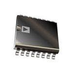
ICGOO电子元器件商城为您提供ADUM3223ARZ由Analog设计生产,在icgoo商城现货销售,并且可以通过原厂、代理商等渠道进行代购。 ADUM3223ARZ价格参考。AnalogADUM3223ARZ封装/规格:隔离器 - 栅极驱动器, 4A Gate Driver Magnetic Coupling 3000Vrms 2 Channel 16-SOIC。您可以下载ADUM3223ARZ参考资料、Datasheet数据手册功能说明书,资料中有ADUM3223ARZ 详细功能的应用电路图电压和使用方法及教程。
Analog Devices Inc.的ADUM3223ARZ是一款双通道数字隔离式栅极驱动器,主要用于驱动功率开关器件,如MOSFET和IGBT。它将高压隔离与高效的栅极驱动能力结合,广泛应用于需要电气隔离和高可靠性的功率电子系统中。

典型应用场景包括:

1. 电机驱动与控制:如工业伺服驱动器、变频器和电机控制器,用于隔离控制电路与功率电路,提升系统安全性和抗干扰能力。

2. 电源转换系统:如DC-DC转换器、AC-DC电源模块,用于驱动功率开关器件,同时提供输入与输出之间的电流隔离,增强系统稳定性。

3. 可再生能源系统:如太阳能逆变器和风能转换系统,用于隔离控制部分与高压功率部分,保障控制电路安全并提升能效。

4. 电动汽车与充电桩:用于电池管理系统(BMS)或车载充电器中,实现高压与低压电路之间的安全隔离,确保控制信号可靠传输。

5. 工业自动化设备:在PLC、工业变频器等设备中,用于驱动高功率负载,同时防止高压侧干扰影响控制电路。

ADUM3223ARZ采用iCoupler®技术,集成隔离与驱动功能,具备高绝缘耐压、低传播延迟和高抗干扰能力,适合复杂电磁环境下的高性能应用需求。
| 参数 | 数值 |
| 产品目录 | |
| ChannelType | 单向 |
| 描述 | OPTOISO 3KV 2CH DRIVER 16SOIC数字隔离器 3kV RMS Prec Half- Bridge Dvr 4A Out |
| 产品分类 | 光隔离器 - 栅极驱动器集成电路 - IC |
| IsolatedPower | 无 |
| 品牌 | Analog Devices |
| 产品手册 | |
| 产品图片 |
|
| rohs | 符合RoHS无铅 / 符合限制有害物质指令(RoHS)规范要求 |
| 产品系列 | 接口 IC,数字隔离器,Analog Devices ADUM3223ARZiCoupler® |
| 数据手册 | |
| 产品型号 | ADUM3223ARZ |
| PCN设计/规格 | |
| PulseWidthDistortion(Max) | - |
| 上升/下降时间(典型值) | 12ns, 12ns |
| 不同If时的传播延迟高-低 | - |
| 产品种类 | |
| 传播延迟tpLH/tpHL(最大值) | 59ns, 59ns |
| 传播延迟时间 | 38 ns |
| 供应商器件封装 | 16-SOIC N |
| 共模瞬态抗扰度(最小值) | 25kV/µs |
| 包装 | 管件 |
| 商标 | Analog Devices |
| 安装类型 | 表面贴装 |
| 安装风格 | SMD/SMT |
| 封装 | Tube |
| 封装/外壳 | 16-SOIC(0.154",3.90mm 宽) |
| 封装/箱体 | SOIC-16 |
| 工作温度 | -40°C ~ 125°C |
| 工厂包装数量 | 48 |
| 技术 | 磁耦合 |
| 数据速率 | 1MHz |
| 最大工作温度 | + 125 C |
| 最大数据速率 | 1.2 Mb/s |
| 最小工作温度 | - 40 C |
| 标准包装 | 48 |
| 电压-正向(Vf)(典型值) | - |
| 电压-电源 | 3 V ~ 5.5 V,4.5 V ~ 18 V |
| 电压-隔离 | 3000Vrms |
| 电流-DC正向(If) | - |
| 电流-峰值输出 | 4A |
| 电流-输出/通道 | 3.2mA |
| 电流-输出高,低 | - |
| 电源电压-最大 | 5 V |
| 电源电压-最小 | 3.3 V |
| 电源电流 | 870 uA, 1.4 mA |
| 类型 | General Purpose |
| 系列 | ADUM3223 |
| 绝缘电压 | 3 kVrms |
| 脉宽失真(最大) | - |
| 视频文件 | http://www.digikey.cn/classic/video.aspx?PlayerID=1364138032001&width=640&height=505&videoID=2219593469001http://www.digikey.cn/classic/video.aspx?PlayerID=1364138032001&width=640&height=505&videoID=2219593470001http://www.digikey.cn/classic/video.aspx?PlayerID=1364138032001&width=640&height=505&videoID=2219614223001 |
| 认可 | UR |
| 输入-输入侧1/输入侧2 | 2/0 |
| 输入类型 | - |
| 输出类型 | 栅极驱动器 |
| 通道数 | 2 |
| 通道数量 | 2 Channel |


- 商务部:美国ITC正式对集成电路等产品启动337调查
- 曝三星4nm工艺存在良率问题 高通将骁龙8 Gen1或转产台积电
- 太阳诱电将投资9.5亿元在常州建新厂生产MLCC 预计2023年完工
- 英特尔发布欧洲新工厂建设计划 深化IDM 2.0 战略
- 台积电先进制程称霸业界 有大客户加持明年业绩稳了
- 达到5530亿美元!SIA预计今年全球半导体销售额将创下新高
- 英特尔拟将自动驾驶子公司Mobileye上市 估值或超500亿美元
- 三星加码芯片和SET,合并消费电子和移动部门,撤换高东真等 CEO
- 三星电子宣布重大人事变动 还合并消费电子和移动部门
- 海关总署:前11个月进口集成电路产品价值2.52万亿元 增长14.8%


PDF Datasheet 数据手册内容提取
Isolated Precision Half-Bridge Driver, 4 A Output Data Sheet ADuM3223/ADuM4223 FEATURES FUNCTIONAL BLOCK DIAGRAM 4 A peak output current ADuM3223/ Working voltage VIA 1 ADuM4223 16 VDDA High-side or low-side relative to input: 537 V peak High-side to low-side differential: 800 V peak VIB 2 ENCODE DECODE 15 VOA High frequency operation: 1 MHz maximum VDD1 3 14 GNDA 3.3 V to 5 V CMOS input logic 4.5 V to 18 V output drive GND1 4 13 NC UVLO at 2.5 V VDD1 DISABLE 5 12 NC ADuM3223A/ADuM4223A UVLO at 4.1 V V DD2 ADuM3223B/ADuM4223B UVLO at 7.0 V V NC 6 11 VDDB DD2 ADuM3223C/ADuM4223C UVLO at 11.0 V VDD2 NC 7 ENCODE DECODE 10 VOB Precise timing characteristics 554 n ns sm maxaixmimuumm c hisaonlanteol-rt aon-cdh darninveerl mpraotpcahginagti on delay VDD1 8NC = NO CONNECT 9 GNDB 10450-001 CMOS input logic levels Figure 1. High common-mode transient immunity: >25 kV/µs GENERAL DESCRIPTION Enhanced system-level ESD performance per IEC 61000-4-x High junction temperature operation: 125°C The ADuM3223/ADuM42231 are 4 A isolated, half-bridge gate Thermal shutdown protection drivers that employ the Analog Devices, Inc., iCoupler® technology Default low output to provide independent and isolated high-side and low-side Safety and regulatory approvals outputs. The ADuM3223 provides 3000 V rms isolation in the ADuM3223 narrow-body, 16-lead SOIC narrow body, 16-lead SOIC package, and the ADuM4223 provides UL recognition per UL 1577 5000 V rms isolation in the wide body, 16-lead SOIC package. 3000 V rms for 1 minute SOIC long package Combining high speed CMOS and monolithic transformer CSA Component Acceptance Notice 5A technology, these isolation components provide outstanding VDE certificate of conformity performance characteristics superior to the alternatives, such as DIN V VDE V 0884-10 (VDE V 0884-10):2006-12 the combination of pulse transformers and gate drivers. V = 560 V peak IORM The ADuM3223/ADuM4223 isolators each provide two ADuM4223 wide-body, 16-lead SOIC independent isolated channels. They operate with an input UL recognition per UL 1577 supply ranging from 3.0 V to 5.5 V, providing compatibility with 5000 V rms for 1 minute SOIC long package lower voltage systems. In comparison to gate drivers employing CSA Component Acceptance Notice 5A high voltage level translation methodologies, the ADuM3223/ VDE certificate of conformity ADuM4223 offer the benefit of true, galvanic isolation between DIN V VDE V 0884-10 (VDE V 0884-10):2006-12 the input and each output. Each output may be continuously V = 849 V peak IORM operated up to 537 V peak relative to the input, thereby supporting Qualified for automotive applications low-side switching to negative voltages. The differential voltage APPLICATIONS between the high-side and low-side may be as high as 800 V peak. Switching power supplies As a result, the ADuM3223/ADuM4223 provide reliable control Isolated IGBT/MOSFET gate drives over the switching characteristics of IGBT/MOSFET configurations Industrial inverters over a wide range of positive or negative switching voltages. Automotive 1 Protected by U.S. Patents 5,952,849; 6,873,065; 7,075,239. Other patents pending. Rev. J Document Feedback Information furnished by Analog Devices is believed to be accurate and reliable. However, no responsibility is assumed by Analog Devices for its use, nor for any infringements of patents or other One Technology Way, P.O. Box 9106, Norwood, MA 02062-9106, U.S.A. rights of third parties that may result from its use. Specifications subject to change without notice. No license is granted by implication or otherwise under any patent or patent rights of Analog Devices. Tel: 781.329.4700 ©2012–2017 Analog Devices, Inc. All rights reserved. Trademarks and registered trademarks are the property of their respective owners. Technical Support www.analog.com
ADuM3223/ADuM4223 Data Sheet TABLE OF CONTENTS Features .............................................................................................. 1 ESD Caution...................................................................................9 Applications ....................................................................................... 1 Pin Configuration and Function Descriptions ........................... 11 Functional Block Diagram .............................................................. 1 Typical Performance Characteristics ........................................... 12 General Description ......................................................................... 1 Applications Information .............................................................. 15 Revision History ............................................................................... 2 PC Board Layout ........................................................................ 15 Specifications ..................................................................................... 3 Propagation Delay-Related Parameters ................................... 15 Electrical Characteristics—5 V Operation ................................ 3 Thermal Limitations and Switch Load Characteristics ......... 15 Electrical Characteristics—3.3 V Operation ............................. 4 Output Load Characteristics ..................................................... 15 Package Characteristics ............................................................... 5 Boot-Strapped Half-Bridge Operation .................................... 16 Insulation and Safety-Related Specifications ............................ 5 DC Correctness and Magnetic Field Immunity........................... 16 Regulatory Information ............................................................... 6 Power Consumption .................................................................. 17 DIN V VDE V 0884-10 (VDE V 0884-10) Insulation Insulation Lifetime ..................................................................... 18 Characteristics .............................................................................. 7 Outline Dimensions ....................................................................... 19 Recommended Operating Conditions ...................................... 8 Ordering Guide .......................................................................... 20 Absolute Maximum Ratings ............................................................ 9 Automotive Products ................................................................. 20 REVISION HISTORY 8/2017—Rev. I to Rev. J 12/2013—Rev. B to Rev. C Added V to GND Negative Transient Parameter, V to GND Change to Features Section .............................................................. 1 OA A OB B Negative Transient Parameter, and Endnote 4, Table 11 .................... 9 Changes to Switching Specifications Parameter, Table 1 ............. 3 Added Thermal Shutdown Temperatures Parameter, Table 1..... 3 3/2017—Rev. H to Rev. I Changes to Switching Specifications Parameter, Table 2 ............. 4 Changes to Table 14 ........................................................................ 11 Added Thermal Shutdown Temperatures Parameter, Table 2..... 4 Changes to Table 10 .......................................................................... 8 1/2017—Rev. G to Rev. H Change to Figure 13 Caption ........................................................ 13 Changes to Table 13 ........................................................................ 10 Changes to Thermal Limitations and Switch Load Characteristics Section .................................................................. 15 11/2015—Rev. F to Rev. G Change to Boot-Strapped Half-Bridge Operation Section ....... 16 Changes to Power Consumption Section .................................... 17 5/2013—Rev. A to Rev. B 7/2015—Rev. E to Rev. F Added V , V Rise Time of 0.5 V/µs; Table 10 ....................... 8 DDA DDB Changes to Features Section............................................................ 1 Changes to Figure 22 ...................................................................... 16 Changes to Table 6 and Table 7 ....................................................... 6 Changes to Power Consumption Section .................................... 17 1/2013—Rev. 0 to Rev. A Added Automotive Information (Throughout) ............................ 1 11/2014—Rev. D to Rev. E Updated Safety and Regulatory Approvals (Throughout) ........... 1 Changes to Features Section and General Description Changed High-Side to Low-Side Differential from 700 V DC PEAK Section ................................................................................................ 1 to 800 V peak ..................................................................................... 1 Changes to Table 5 ............................................................................ 5 Added R , R Minimum and Maximum Values, Table 1 ......... 3 OA OB Changes to Regulatory Information Section, Table 6, and Added R , R Minimum and Maximum Values, Table 2 ......... 4 OA OB Table 7 ................................................................................................ 6 Changes to Table 13 ....................................................................... 10 Changes to Table 8 and Table 9 ....................................................... 7 Changes to Figure 19 ...................................................................... 15 Added Boot-Strapped Half Bridge Operation Section and 4/2014—Rev. C to Rev. D Figure 22; Renumbered Sequentially ........................................... 16 Changes to Applications Section .................................................... 1 Changes to Ordering Guide .......................................................... 20 Changes to Insulation Lifetime Section ....................................... 18 Changes to Ordering Guide .......................................................... 20 5/2012—Revision 0: Initial Version Rev. J | Page 2 of 20
Data Sheet ADuM3223/ADuM4223 SPECIFICATIONS ELECTRICAL CHARACTERISTICS—5 V OPERATION All voltages are relative to their respective ground. 4.5 V ≤ V ≤ 5.5 V, 4.5 V ≤ V ≤ 18 V, unless stated otherwise. All minimum/ DD1 DD2 maximum specifications apply over T = −40°C to 125°C. All typical specifications are at T = 25°C, V = 5 V, V = 12 V. Switching J J DD1 DD2 specifications are tested with CMOS signal levels. Table 1. Parameter Symbol Min Typ Max Unit Test Conditions DC SPECIFICATIONS Input Supply Current, Quiescent IDDI(Q) 1.4 2.4 mA Output Supply Current, Per Channel, Quiescent IDDO(Q) 2.3 3.2 mA Supply Current at 1 MHz VDD1 Supply Current IDD1(Q) 1.6 2.5 mA Up to 1 MHz, no load VDDA/VDDB Supply Current IDDA/IDDB(Q) 5.6 8.0 mA Up to 1 MHz, no load Input Currents IIA, IIB −1 +0.01 +1 µA 0 ≤ VIA, VIB ≤ VDD1 Logic High Input Threshold VIH 0.7 × VDD1 V Logic Low Input Threshold VIL 0.3 × VDD1 V Logic High Output Voltages VOAH, VOBH VDD2 – 0.1 VDD2 V IOx = −20 mA, VIx = VIxH Logic Low Output Voltages VOAL, VOBL 0.0 0.15 V IOx = +20 mA, VIx = VIxL Undervoltage Lockout, VDD2 Supply Positive Going Threshold VDD2UV+ 4.1 4.4 V A-grade Negative Going Threshold VDD2UV− 3.2 3.6 V A-grade Hysteresis VDD2UVH 0.5 V A-grade Positive Going Threshold VDD2UV+ 6.9 7.4 V B-grade Negative Going Threshold VDD2UV− 5.7 6.2 V B-grade Hysteresis VDD2UVH 0.7 V B-grade Positive Going Threshold VDD2UV+ 10.5 11.1 V C-grade Negative Going Threshold VDD2UV− 8.9 9.6 V C-grade Hysteresis VDD2UVH 0.9 V C-grade Output Short-Circuit Pulsed Current1 IOA(SC), IOB(SC) 2.0 4.0 A VDD2 = 12 V Output Pulsed Source Resistance ROA, ROB 0.3 1.1 3.0 Ω VDD2 = 12 V Output Pulsed Sink Resistance ROA, ROB 0.3 0.6 3.0 Ω VDD2 = 12 V THERMAL SHUTDOWN TEMPERATURES Junction Temperature Shutdown, Rising Edge TJR 150 °C Junction Temperature Shutdown, Falling Edge TJF 140 °C SWITCHING SPECIFICATIONS Pulse Width2 PW 50 ns CL = 2 nF, VDD2 = 12 V Maximum Data Rate3 1 MHz CL = 2 nF, VDD2 = 12 V Propagation Delay4 tDHL, tDLH 31 43 54 ns CL = 2 nF, VDD2 = 12 V; see Figure 20 ADuM3223A/ADuM4223A tDHL, tDLH 35 47 59 ns CL = 2 nF, VDD2 = 4.5 V; see Figure 20 Propagation Delay Skew5 tPSK 12 ns CL = 2 nF, VDD2 = 12 V; see Figure 20 Channel-to-Channel Matching6 tPSKCD 1 5 ns CL = 2 nF, VDD2 = 12 V; see Figure 20 tPSKCD 1 7 ns CL = 2 nF, VDD2 = 4.5 V; see Figure 20 Output Rise/Fall Time (10% to 90%) tR/tF 6 12 18 ns CL = 2 nF, VDD2 = 12 V; see Figure 20 Dynamic Input Supply Current Per Channel IDDI(D) 0.05 mA/Mbps VDD2 = 12 V Dynamic Output Supply Current Per Channel IDDO(D) 1.65 mA/Mbps VDD2 = 12 V Refresh Rate fr 1.2 Mbps 1 Short-circuit duration less than 1 µs. Average power must conform to the limit shown under the Absolute Maximum Ratings. 2 The minimum pulse width is the shortest pulse width at which the specified timing parameter is guaranteed. 3 The maximum data rate is the fastest data rate at which the specified timing parameter is guaranteed. 4 tDLH propagation delay is measured from the time of the input rising logic high threshold, VIH, to the output rising 10% level of the VOx signal. tDHL propagation delay is measured from the input falling logic low threshold, VIL, to the output falling 90% threshold of the VOx signal. See Figure 20 for waveforms of propagation delay parameters. 5 tPSK is the magnitude of the worst-case difference in tDLH and/or tDHL that is measured between units at the same operating temperature, supply voltages, and output load within the recommended operating conditions. See Figure 20 for waveforms of propagation delay parameters. 6 Channel-to-channel matching is the absolute value of the difference in propagation delays between the two channels. Rev. J | Page 3 of 20
ADuM3223/ADuM4223 Data Sheet ELECTRICAL CHARACTERISTICS—3.3 V OPERATION All voltages are relative to their respective ground. 3.0 V ≤ V ≤ 3.6 V, 4.5 V ≤ V ≤ 18 V, unless stated otherwise. All minimum/ DD1 DD2 maximum specifications apply over T = −40°C to 125°C. All typical specifications are at T = 25°C, V = 3.3 V, V = 12 V. Switching J J DD1 DD2 specifications are tested with CMOS signal levels. Table 2. Parameter Symbol Min Typ Max Unit Test Conditions DC SPECIFICATIONS Input Supply Current, Quiescent IDDI(Q) 0.87 1.4 mA Output Supply Current, Per Channel, Quiescent IDDO(Q) 2.3 3.2 mA Supply Current at 1 MHz VDD1 Supply Current IDD1(Q) 1.1 1.5 mA Up to 1 MHz, no load VDDA/VDDB Supply Current IDDA/IDDB(Q) 5.6 8.0 mA Up to 1 MHz, no load Input Currents IIA, IIB −10 +0.01 +10 µA 0 ≤ VIA, VIB ≤ VDD1 Logic High Input Threshold VIH 0.7 × VDD1 V Logic Low Input Threshold VIL 0.3 × VDD1 V Logic High Output Voltages VOAH, VOBH VDD2 – 0.1 VDD2 V IOx = −20 mA, VIx = VIxH Logic Low Output Voltages VOAL, VOBL 0.0 0.15 V IOx = +20 mA, VIx = VIxL Undervoltage Lockout, VDD2 Supply Positive Going Threshold VDD2UV+ 4.1 4.4 V A-grade Negative Going Threshold VDD2UV− 3.2 3.6 V A-grade Hysteresis VDD2UVH 0.5 V A-grade Positive Going Threshold VDD2UV+ 6.9 7.4 V B-grade Negative Going Threshold VDD2UV− 5.7 6.2 V B-grade Hysteresis VDD2UVH 0.7 V B-grade Positive Going Threshold VDD2UV+ 10.5 11.1 V C-grade Negative Going Threshold VDD2UV− 8.9 9.6 V C-grade Hysteresis VDD2UVH 0.9 V C-grade Output Short-Circuit Pulsed Current1 IOA(SC), IOB(SC) 2.0 4.0 A VDD2 = 12 V Output Pulsed Source Resistance ROA, ROB 0.3 1.1 3.0 Ω VDD2 = 12 V Output Pulsed Sink Resistance ROA, ROB 0.3 0.6 3.0 Ω VDD2 = 12 V THERMAL SHUTDOWN TEMPERATURE Junction Temperature Shutdown, Rising Edge TJR 150 °C Junction Temperature Shutdown, Falling Edge TJF 140 °C SWITCHING SPECIFICATIONS Pulse Width2 PW 50 ns CL = 2 nF, VDD2 = 12 V Maximum Data Rate3 1 MHz CL = 2 nF, VDD2 = 12 V Propagation Delay4 tDHL, tDLH 35 47 59 ns CL = 2 nF, VDD2 = 12 V, see Figure 20 ADuM3223A/ADuM4223A tDHL, tDLH 37 51 65 ns CL = 2 nF, VDD2 = 4.5 V, see Figure 20 Propagation Delay Skew5 tPSK 12 ns CL = 2 nF, VDD2 = 12 V, see Figure 20 Channel-to-Channel Matching6 tPSKCD 1 5 ns CL = 2 nF, VDD2 = 12 V, see Figure 20 tPSKCD 1 7 ns CL = 2 nF, VDD2 = 4.5 V, see Figure 20 Output Rise/Fall Time (10% to 90%) tR/tF 6 12 22 ns CL = 2 nF, VDD2 = 12 V, see Figure 20 Dynamic Input Supply Current Per Channel IDDI(D) 0.05 mA/Mbps VDD2 = 12 V Dynamic Output Supply Current Per Channel IDDO(D) 1.65 mA/Mbps VDD2 = 12 V Refresh Rate fr 1.1 Mbps 1 Short-circuit duration less than 1 µs. Average power must conform to the limit shown under the Absolute Maximum Ratings. 2 The minimum pulse width is the shortest pulse width at which the specified timing parameter is guaranteed. 3 The maximum data rate is the fastest data rate at which the specified timing parameter is guaranteed. 4 tDLH propagation delay is measured from the time of the input rising logic high threshold, VIH, to the output rising 10% level of the VOx signal. tDHL propagation delay is measured from the input falling logic low threshold, VIL, to the output falling 90% threshold of the VOx signal. See Figure 20 for waveforms of propagation delay parameters. 5 tPSK is the magnitude of the worst-case difference in tDLH and/or tDHL that is measured between units at the same operating temperature, supply voltages, and output load within the recommended operating conditions. See Figure 20 for waveforms of propagation delay parameters. 6 Channel-to-channel matching is the absolute value of the difference in propagation delays between the two channels. Rev. J | Page 4 of 20
Data Sheet ADuM3223/ADuM4223 PACKAGE CHARACTERISTICS Table 3. Parameter Symbol Min Typ Max Unit Test Conditions Resistance (Input-to-Output) R 1012 Ω I-O Capacitance (Input-to-Output) C 2.0 pF f = 1 MHz I-O Input Capacitance C 4.0 pF I IC Junction-to-Ambient Thermal Resistance ADuM3223 θ 76 °C/W JA ADuM4223 θ 45 °C/W JA IC Junction-to-Case Thermal Resistance ADuM3223 θ 42 °C/W JC ADuM4223 θ 29 °C/W JC INSULATION AND SAFETY-RELATED SPECIFICATIONS ADuM3223 Table 4. Parameter Symbol Value Unit Conditions Rated Dielectric Insulation Voltage 3000 V rms 1 minute duration Minimum External Air Gap (Clearance) L(I01) 4.0 min mm Measured from input terminals to output terminals, shortest distance through air Minimum External Tracking (Creepage) L(I02) 4.0 min mm Measured from input terminals to output terminals, shortest distance path along body Minimum Internal Gap (Internal Clearance) 0.017 min mm Insulation distance through insulation Tracking Resistance (Comparative Tracking Index) CTI >400 V DIN IEC 112/VDE 0303 Part 1 Isolation Group II Material Group (DIN VDE 0110, 1/89, Table 1) ADuM4223 Table 5. Parameter Symbol Value Unit Conditions Rated Dielectric Insulation Voltage 5000 V rms 1 minute duration Minimum External Air Gap (Clearance) L(I01) 7.6 min mm Measured from input terminals to output terminals, shortest distance through air Minimum External Tracking (Creepage) L(I02) 7.6 min mm Measured from input terminals to output terminals, shortest distance path along body Minimum Internal Gap (Internal Clearance) 0.017 min mm Insulation distance through insulation Tracking Resistance (Comparative Tracking Index) CTI >400 V DIN IEC 112/VDE 0303 Part 1 Isolation Group II Material Group (DIN VDE 0110, 1/89, Table 1) Rev. J | Page 5 of 20
ADuM3223/ADuM4223 Data Sheet REGULATORY INFORMATION The ADuM3223 is approved or pending approval by the organizations listed in Table 6. Table 6. UL CSA VDE Recognized under UL 1577 Approved under CSA Component Acceptance Notice 5A Certified according to DIN V VDE V 0884-10 Component Recognition (VDE V 0884-10): 2006-122 Program1 Single/Protection 3000 V rms Basic insulation per CSA 60950-1-07 and IEC 60950-1, Reinforced insulation, 560 V peak Isolation Voltage 380 V rms (537 V peak) maximum working voltage File E214100 File 205078 File 2471900-4880-0001 1 In accordance with UL 1577, each ADuM3223 is proof tested by applying an insulation test voltage ≥ 3600 V rms for 1 second (current leakage detection limit = 6 µA). 2 In accordance with DIN V VDE V 0884-10, each ADuM3223 is proof tested by applying an insulation test voltage ≥ 1050 V peak for 1 second (partial discharge detection limit = 5 pC). An asterisk (*) marking branded on the component designates DIN V VDE V 0884-10 approval. The ADuM4223 is approved or pending approval by the organizations listed in Table 7. Table 7. UL CSA CQC VDE Recognized Under Approved under CSA Component Approved under CQC11-471543-2012 Certified according to UL 1577 Component Acceptance Notice 5A DIN V VDE V 0884-10 Recognition Program1 (VDE V 0884-10): 2006- 122 Single/Protection Reinforced insulation per Reinforced insulation per GB4943.1-2011, Reinforced insulation, 5000 V rms Isolation CSA 60950-1-07 and IEC 60950-1, 380 V rms (537 V peak) maximum working 849 V peak Voltage 380 V rms (537 V peak) maximum voltage, tropical climate, altitude ≤ 5000 m; working voltage; basic insulation basic insulation per GB4943.1-2011, per CSA 60950-1-07 and IEC 60950-1, 600 V rms (848 V peak) maximum working 760 V rms (1074 V peak) maximum voltage, tropical climate, altitude ≤ 5000 m working voltage File E214100 File 205078 File CQC14001108627 File 2471900-4880-0001 1 In accordance with UL 1577, each ADuM4223 is proof tested by applying an insulation test voltage ≥ 6000 V rms for 1 second (current leakage detection limit = 10 µA). 2 In accordance with DIN V VDE V 0884-10, each ADuM4223 is proof tested by applying an insulation test voltage ≥ 1592 V peak for 1 second (partial discharge detection limit = 5 pC). An asterisk (*) marking branded on the component designates DIN V VDE V 0884-10 approval. Rev. J | Page 6 of 20
Data Sheet ADuM3223/ADuM4223 DIN V VDE V 0884-10 (VDE V 0884-10) INSULATION CHARACTERISTICS These isolators are suitable for reinforced isolation only within the safety limit data. Maintenance of the safety data is ensured by protective circuits. The asterisk (*) marking on the package denotes DIN V VDE V 0884-10 approval for a 560 V peak working voltage. Table 8. ADuM3223 VDE Characteristics Description Conditions Symbol Characteristic Unit Installation Classification per DIN VDE 0110 For Rated Mains Voltage ≤ 150 V rms I to IV For Rated Mains Voltage ≤ 300 V rms I to III For Rated Mains Voltage ≤ 400 V rms I to II Climatic Classification 40/105/21 Pollution Degree per DIN VDE 0110, Table 1 2 Maximum Working Insulation Voltage V 560 V peak IORM Input-to-Output Test Voltage, Method B1 V × 1.875 = V , 100% production test, V 1050 V peak IORM pd(m) pd(m) t = t = 1 sec, partial discharge < 5 pC ini m Input-to-Output Test Voltage, Method A V × 1.5 = V , t = 60 sec, V IORM pd(m) ini pd(m) t = 10 sec, partial discharge < 5 pC m After Environmental Tests Subgroup 1 896 V peak After Input and/or Safety Test Subgroup 2 V × 1.2 = V , t = 60 sec, V 672 V peak IORM pd(m) ini pd(m) and Subgroup 3 t = 10 sec, partial discharge < 5 pC m Highest Allowable Overvoltage V 4242 V peak IOTM Surge Isolation Voltage V = 10 kV, 1.2 µs rise time, 50 µs, 50% fall time V 6000 V peak PEAK IOSM Safety-Limiting Values Maximum value allowed in the event of a failure (see Figure 2) Maximum Junction Temperature T 150 °C S Safety Total Dissipated Power P 1.64 W S Insulation Resistance at T V = 500 V R >109 Ω S IO S Table 9. ADuM4223 VDE Characteristics Description Conditions Symbol Characteristic Unit Installation Classification per DIN VDE 0110 For Rated Mains Voltage ≤ 150 V rms I to IV For Rated Mains Voltage ≤ 300 V rms I to III For Rated Mains Voltage ≤ 400 V rms I to II Climatic Classification 40/105/21 Pollution Degree per DIN VDE 0110, Table 1 2 Maximum Working Insulation Voltage V 849 V peak IORM Input-to-Output Test Voltage, Method B1 V × 1.875 = V , 100% production test, V 1592 V peak IORM pd(m) pd(m) t = t = 1 sec, partial discharge < 5 pC ini m Input-to-Output Test Voltage, Method A V × 1.5 = V , t = 60 sec, t = 10 sec, V IORM pd(m) ini m pd(m) partial discharge < 5 pC After Environmental Tests Subgroup 1 1273 V peak After Input and/or Safety Test Subgroup 2 V × 1.2 = V , t = 60 sec, t = 10 sec, V 1018 V peak IORM pd(m) ini m pd(m) and Subgroup 3 partial discharge < 5 pC Highest Allowable Overvoltage V 7071 V peak IOTM Surge Isolation Voltage V = 10 kV, 1.2 µs rise time, 50 µs, 50% fall time V 6000 V peak PEAK IOSM Safety-Limiting Values Maximum value allowed in the event of a failure (see Figure 3) Maximum Junction Temperature T 150 °C S Safety Total Dissipated Power P 2.77 W S Insulation Resistance at T V = 500 V R >109 Ω S IO S Rev. J | Page 7 of 20
ADuM3223/ADuM4223 Data Sheet W) RECOMMENDED OPERATING CONDITIONS R ( 1.8 E OW 1.6 Table 10. P DB 1.4 Parameter Symbol Min Max Unit D OR PV 1.2 OpTeermatpinegra Jtuunrec tion TJ −40 +125 °C A D 1.0 Supply Voltages1 D V , PD1 0.8 VDD1 3.0 5.5 V D V , V 4.5 18 V V DDA DDB P 0.6 NG VDD1 Rise Time TVDD1 1 V/µs ATI 0.4 VDDA, VDDB Rise Time TVDDA, TVDDB 10 V/µs R PE 0.2 Maximum Input Signal Rise TVIA, TVIB 1 ms O E and Fall Times SAF 00 50AMBIENT TEM10P0ERATURE (°C1)50 200 10450-102 CoImmmmounn-iMtyo, Sdtea tTicra2 nsient −50 +50 kV/µs Figure 2. ADuM3223 Thermal Derating Curve, Dependence of Common-Mode Transient −25 +25 kV/µs Safety-Limiting Values on Case Temperature, per DIN V VDE V 0884-10 Immunity, Dynamic3 1 All voltages are relative to their respective ground. See the Applications Information section for information on immunity to external magnetic fields. W) ER ( 3.0 2 Sbteattwice ceonm GmNoDn1 -amndod GeN tDraAn/GsiNenDtB i,m wmithu ninitpyu itss d heeflidn eedit hase rt hheig lhar ogre lsot wd vs/udcth OW that the output voltage remains either above 0.8 × VDD2 for VIA/VIB = high or PDB 2.5 0le.8ve Vls f omr aVyIA c/VauIBs =e lmowom. Oepnetraartyi odna twa iuthp steratns.s ients above the recommended D PV 3 Dynamic common-mode transient immunity is defined as the largest dv/dt OR 2.0 between GND1 and GNDA/GNDB, with the switching edge coincident with A the transient test pulse. Operation with transients above the recommended DD levels may cause momentary data upsets. PV 1.5 , D1 D V P 1.0 G N TI A R 0.5 E P O E SAF 00 50AMBIENT TEM10P0ERATURE (°C1)50 200 10450-103 Figure 3. ADuM4223 Thermal Derating Curve, Dependence of Safety-Limiting Values on Case Temperature, per DIN V VDE V 0884-10 Rev. J | Page 8 of 20
Data Sheet ADuM3223/ADuM4223 ABSOLUTE MAXIMUM RATINGS Ambient temperature = 25°C, unless otherwise noted. Stresses at or above those listed under Absolute Maximum Table 11. Ratings may cause permanent damage to the product. This is a Parameter Symbol Rating stress rating only; functional operation of the product at these Storage Temperature T −55°C to +150°C or any other conditions above those indicated in the operational ST Operating Junction T −40°C to +150°C section of this specification is not implied. Operation beyond J Temperature the maximum operating conditions for extended periods may Supply Voltages1 VDD1 −0.5 V to +7.0 V affect product reliability. V , V −0.5 V to +20 V DDA DDB ESD CAUTION Input Voltage1 V , V , −0.5 V to V + 0.5 V IA IB DD1 DISABLE Output Voltage1 V −0.5 V to V + 0.5 V OA DDA V −0.5 V to V + 0.5 V OB DDB Average Output I −35 mA to +35 mA O Current, per Pin2 V to GND Negative V −2 V for 100 ns OA A OA Transient4 V to GND Negative V −2 V for 100 ns OB B OB Transient4 Common-Mode CM , CM −100 kV/µs to +100 kV/µs H L Transients3 1 All voltages are relative to their respective ground. 2 See Figure 2 and Figure 3 for information on maximum allowable current for various temperatures. 3 Refers to common-mode transients across the insulation barrier. Common- mode transients exceeding the absolute maximum rating can cause latch-up or permanent damage. 4 Applies to non-automotive grade parts only. Rev. J | Page 9 of 20
ADuM3223/ADuM4223 Data Sheet Table 12. Maximum Continuous Working Voltage1 Parameter Max Unit Constraint AC Voltage, Bipolar Waveform 565 V peak 50-year minimum lifetime AC Voltage, Unipolar Waveform 1131 V peak 50-year minimum lifetime DC Voltage 1131 V peak 50-year minimum lifetime 1 Refers to the continuous voltage magnitude imposed across the isolation barrier. See the Insulation Lifetime section for more details. Table 13. Truth Table ADuM3223/ADuM4223 (Positive Logic)1 V V IA IB DISABLE2 Input Input V State V /V State V Output V Output Notes DD1 DDA DDB OA OB L L L Powered Powered L L L L H Powered Powered L H L H L Powered Powered H L L H H Powered Powered H H H X X Powered Powered L L L L L Unpowered Powered L L Outputs return to the input state within 1 µs of V power restoration. DD1 X X X Powered Unpowered L L Outputs return to the input state within 50 µs of V /V power DDA DDB restoration. 1 X means don’t care, L means low, and H means high. 2 Reaction to DISABLE is approximately one propagation delay. Rev. J | Page 10 of 20
Data Sheet ADuM3223/ADuM4223 PIN CONFIGURATION AND FUNCTION DESCRIPTIONS VIA 1 16 VDDA VIB 2 15 VOA ADuM3223/ VDD1 3 ADuM4223 14 GNDA GND1 4 TOP VIEW 13 NC DISABLE 5 (Not to Scale) 12 NC NC 6 11 VDDB NC 7 10 VOB VDD1 8 9 GNDB N1.ONDTCOE S=N ONOT CCOONNNNEECCTT .TO THIS PIN. 10450-003 Figure 4. Pin Configuration Table 14. ADuM3223/ADuM4223 Pin Function Descriptions Pin No.1 Mnemonic Description 1 V Logic Input A. IA 6, 7, 12, 13 NC No Connect. Do not connect to this pin 2 V Logic Input B. IB 3, 8 V Input Supply Voltage. DD1 4 GND Ground Reference for Input Logic Signals. 1 5 DISABLE Input Disable. When this pin is high, it disables the isolator inputs setting outputs to a low state. The reaction to the DISABLE pin signal is approximately equal to the normal propagation delay. 9 GND Ground Reference for Output B. B 10 V Output B. OB 11 V Output B Supply Voltage. DDB 14 GND Ground Reference for Output A. A 15 V Output A. OA 16 V Output A Supply Voltage. DDA 1 Pin 3 and Pin 8 are internally connected; connecting both pins to supply VDD1 is recommended. For specific layout guidelines, refer to the AN-1109 Application Note, Recommendations for Control of Radiated Emissions with iCoupler Devices. Rev. J | Page 11 of 20
ADuM3223/ADuM4223 Data Sheet TYPICAL PERFORMANCE CHARACTERISTICS 1000 800 CH2 = VO (5V/DIV) VDD2 = 5V C) n E ( 600 G R 2 HA C E 400 VDD2 = 8V T A G CH1 = VI (5V/DIV) VDD2 = 10V 200 1 VDD2 = 15V 0 CH1 5.00V CH1 5.00V Ω M21.045000k.G 0PSnOs/sINTS A CH1 2.70V 10450-105 0 200 SWITCH4I0N0G FREQUE6N00CY (kHz) 800 1000 10450-108 Figure 5. Output Waveform for 2 nF Load with Figure 8. Typical ADuM4223 Maximum Load vs. Frequency (RG = 1 Ω) 12 V Output Supply a b a –820ps 1.40V 3.0 b 10.5ns 11.4V ∆11.3ns ∆10.0V 2.5 CH2 = VOB (5V/DIV) A) 2.0 m T ( VDD1 = 5V N 2 RE 1.5 R U CH1 = VOA (5V/DIV) I CDD1 1.0 VDD1 = 3.3V 0.5 1 0 CH1 5.00V CH2 5.00V Ω M21.025000k.G 0PSnOs/sINTS A CH1 2.70V 10450-106 0 0.25 FREQUE0N.5C0Y (MHz) 0.75 1.00 10450-109 Figure 6. Output Matching and Rise Time Waveforms for 2 nF Load Figure 9. Typical IDD1 Supply Current vs. Frequency with 12 V Output Supply 500 50 400 40 A) VDD2 = 15V RGE (nC) 300 VDD2 = 5V RRENT (m 30 VDD2 = 10V A U H C E C 200 VDD2 = 8V DB 20 T D GA VDD2 = 10V , IDA VDD2 = 5V D I 100 10 VDD2 = 15V 0 0 0 200 SWITCH4I0N0G FREQUE6N00CY (kHz) 800 1000 10450-107 0 0.25 FREQUE0N.5C0Y (MHz) 0.75 1.00 10450-110 Figure 7. Typical ADuM3223 Maximum Load vs. Frequency (RG = 1 Ω) Figure 10. Typical IDDA, IDDB Supply Current vs. Frequency with 2 nF Load Rev. J | Page 12 of 20
Data Sheet ADuM3223/ADuM4223 60 30 50 25 ns) tDHL ON DELAY ( 4300 tDLH L TIME (ns) 2105 TI AL FALL TIME A F OPAG 20 RISE/ 10 RISE TIME R P 10 5 0 0 –40 –20 0 JUNC20TION 4T0EMPE6R0ATUR8E0 (°C)100 120 140 10450-111 5 7 OU9TPUT SUP11PLY VOL1T3AGE (V)15 17 10450-114 Figure 11. Typical Propagation Delay vs. Temperature Figure 14. Typical Rise/Fall Time Variation vs. Output Supply Voltage 60 5 s) n G ( 50 N HI 4 Y (ns) 40 tDHL MATC DELA tDLH H-CH 3 ON 30 Y C TI A PAGA 20 N DEL 2 PRO GATIO 1 PD MATCHtDLH PD MATCHtDHL 10 A P O R P 0 0 3.0 3.5 INPUT S4.U0PPLY VOL4T.5AGE (V) 5.0 5.5 10450-112 5 7 OU9TPUT SUP11PLY VOL1T3AGE (V)15 17 10450-115 Figure 12. Typical Propagation Delay vs. Input Supply Voltage, Figure 15. Typical Propagation Delay, Channel-to-Channel Matching vs. VDDA, VDDB = 12 V Output Supply Voltage 60 5 s) n G ( 50 N HI 4 Y (ns) 40 tDHL MATC DELA tDLH H-CH 3 ON 30 Y C PAGATI 20 N DELA 2 O O PR ATI PD MATCHtDLH G 1 10 PA PD MATCHtDHL O R P 0 0 5 7 OU9TPUT SUP11PLY VOL1T3AGE (V)15 17 10450-113 –40 –20 0 JUNC20TION 4T0EMPE6R0ATUR8E0 (°C)100 120 140 10450-116 Figure 13. Typical Propagation Delay vs. Output Supply Voltage, Figure 16. Typical Propagation Delay, Channel-to-Channel Matching vs. VDD1 = 5 V Temperature, VDDA, VDDB = 12 V Rev. J | Page 13 of 20
ADuM3223/ADuM4223 Data Sheet 1.6 8 1.4 7 1.2 VOUT SOURCE RESISTANCE T (A) 6 SINK IOUT N 1.0 RE 5 Ω) UR (UT 0.8 K C 4 RO 0.6 VOUT SINK RESISTANCE E/SIN 3 SOURCE IOUT C R U 0.4 O 2 S 0.2 1 04 6 OU8TPUT S1U0PPLY V1O2LTAGE1 (4V) 16 18 10450-117 04 6 OU8TPUT S1U0PPLY V1O2LTAGE1 (4V) 16 18 10450-118 Figure 17. Typical Output Resistance vs. Output Supply Voltage Figure 18. Typical Output Current vs. Output Supply Voltage Rev. J | Page 14 of 20
Data Sheet ADuM3223/ADuM4223 APPLICATIONS INFORMATION PC BOARD LAYOUT Channel-to-channel matching refers to the maximum amount that the propagation delay differs between channels within a The ADuM3223/ADuM4223 digital isolators require no external single ADuM3223/ADuM4223 component. interface circuitry for the logic interfaces. Power supply bypassing is required at the input and output supply pins, as shown in Propagation delay skew refers to the maximum amount that Figure 19. Use a small ceramic capacitor with a value between the propagation delay differs between multiple ADuM3223/ 0.01 μF and 0.1 μF to provide a good high frequency bypass. ADuM4223 components operating under the same conditions. On the output power supply pin, VDDA or VDDB, it is also recom- THERMAL LIMITATIONS AND SWITCH LOAD mended to add a 10 μF capacitor to provide the charge required CHARACTERISTICS to drive the gate capacitance at the ADuM3223/ADuM4223 For isolated gate drivers, the necessary separation between the outputs. On the output supply pin, the bypass capacitor use of input and output circuits prevents the use of a single thermal vias must be avoided or multiple vias must be employed to pad beneath the part, and heat is, therefore, dissipated mainly reduce the inductance in the bypassing. The total lead length through the package pins. between both ends of the smaller capacitor and the input or output power supply pin must not exceed 5 mm. Package thermal dissipation limits the performance of switching frequency vs. output load, as illustrated in Figure 7 and Figure 8 VIA VDDA for the maximum load capacitance that can be driven with a 1 Ω VIB VOA series gate resistance for different values of output voltage. For VDD1 GNDA example, this curve shows that a typical ADuM3223 can drive a GND1 NC large MOSFET with 140 nC gate charge at 8 V output (which is DISABLE NC equivalent to a 17 nF load) up to a frequency of about 300 kHz. NC VDDB Each of the ADuM3223/ADuM4223 isolator outputs has a thermal NC VOB shutdown protection function, which sets an output to a logic VDD1 GNDB 10450-119 low when the rising junction temperature typically reaches 150°C, and turns back on after the junction temperature falls Figure 19. Recommended PCB Layout from the shutdown by approximately 10°C. PROPAGATION DELAY-RELATED PARAMETERS OUTPUT LOAD CHARACTERISTICS Propagation delay is a parameter that describes the time it takes The ADuM3223/ADuM4223 output signals depend on the a logic signal to propagate through a component. The propagation characteristics of the output load, which is typically an N-channel delay to a logic low output can differ from the propagation delay MOSFET. The driver output response to an N-channel MOSFET to a logic high output. The ADuM3223/ADuM4223 specify t DLH load can be modeled with a switch output resistance (R ), an (see Figure 20) as the time between the rising input high logic SW inductance due to the printed circuit board trace (L ), a series threshold, V , to the output rising 10% threshold. Likewise, the TRACE IH gate resistor (R ), and a gate-to-source capacitance (C ), as falling propagation delay, t , is defined as the time between GATE GS DHL shown in Figure 21. the input falling logic low threshold, V , and the output falling IL 90% threshold. The rise and fall times are dependent on the ldoealadyin, wg hcoicnhd iist itohnes iannddu satrrey n sotat nindcalrudd feodr igna tteh ed rpirvoeprsa.g ation VIA AADDuuMM34222233/ VOA RSWLTRACERGATE CGSVO 10450-006 90% Figure 21. RLC Model of the Gate of an N-Channel MOSFET OUTPUT R is the switch resistance of the internal ADuM3223/ADuM4223 SW 10% driver output, which is about 1.1 Ω. RGATE is the intrinsic gate resistance of the MOSFET and any external series resistance. A MOSFET that requires a 4 A gate driver has a typical intrinsic VIH INPUT gate resistance of about 1 Ω and a gate-to-source capacitance, VIL C , of between 2 nF and 10 nF. L is the inductance of the GS TRACE t tDHL printed circuit board trace, typically a value of 5 nH or less for a DLH tR tF 10450-005 wtheel lA-dDesuiMgn3e2d2 l3ay/AouDt uwMith42 a2 v3e oryu tsphuotr tt oa nthde w giadtee coofn tnheec MtioOnS fFrEomT. Figure 20. Propagation Delay Parameters Rev. J | Page 15 of 20
ADuM3223/ADuM4223 Data Sheet The following equation defines the Q factor of the RLC circuit, DC CORRECTNESS AND MAGNETIC FIELD IMMUNITY which indicates how the ADuM3223/ADuM4223 output responds Positive and negative logic transitions at the isolator input cause to a step change. For a well-damped output, Q is less than 1. narrow (~1 ns) pulses to be sent to the decoder via the transformer. Adding a series gate resistance dampens the output response. The decoder is bistable and is, therefore, either set or reset by 1 L the pulses, indicating input logic transitions. In the absence of Q= × TRACE (R +R ) C logic transitions of more than 1 µs at the input, a periodic set of SW GATE GS refresh pulses indicative of the correct input state are sent to In Figure 5, the ADuM3223/ADuM4223 output waveforms for ensure dc correctness at the output. a 12 V output are shown for a C of 2 nF. Note the small amount of GS If the decoder receives no internal pulses for more than about ringing of the output in Figure 5 with C of 2 nF, R of 1.1 Ω, GS SW 3 µs, the input side is assumed to be unpowered or nonfunctional, R of 0 Ω, and a calculated Q factor of 0.75, where less than 1 GATE in which case, the isolator output is forced to a default low state is desired for good damping. by the watchdog timer circuit. In addition, the outputs are in a Output ringing can be reduced by adding a series gate resistance low default state while the power is coming up before the to dampen the response. For applications of less than 1 nF load, UVLO threshold is crossed. it is recommended to add a series gate resistor of about 2 Ω to 5 Ω. The ADuM3223/ADuM4223 is immune to external magnetic BOOT-STRAPPED HALF-BRIDGE OPERATION fields. The limitation on the ADuM3223/ADuM4223 magnetic field immunity is set by the condition in which induced voltage The ADuM3223/ADuM4223 are well suited to the operation of in the transformer receiving coil is sufficiently large to either two output gate signals that are referenced to separate grounds, falsely set or reset the decoder. The following analysis defines as in the case of a half-bridge configuration. Because isolated the conditions under which this can occur. The 3 V operating auxiliary supplies are often expensive, it is beneficial to reduce condition of the ADuM3223/ADuM4223 is examined because the amount of supplies. One method to perform this is to use a it represents the most susceptible mode of operation. The pulses boot-strap configuration for the high-side supply of the at the transformer output have an amplitude greater than 1.0 V. ADuM3223/ADuM4223. In this topology, the decoupling The decoder has a sensing threshold at about 0.5 V, therefore capacitor, C , acts as the energy storage for the high-side supply, A establishing a 0.5 V margin in which induced voltages can be and is filled whenever the low-side switch is closed, bringing tolerated. The voltage induced across the receiving coil is given by GND to GND . During the charging time of C , the dv/dt of A B A the VDDA voltage must be controlled to reduce the possibility of V = (−dβ/dt) ∑π rn2, n = 1, 2, ... , N glitches on the output. Keeping the dv/dt below 10 V/µs is where: recommended for the ADuM3223/ADuM4223. This can be β is the magnetic flux density (gauss). controlled by introducing a series resistance, R , into the BOOT N is the number of turns in the receiving coil. charging path of C . As an example, if V is 12 V, C has a A AUX A r is the radius of the nth turn in the receiving coil (cm). n total capacitance of 10 µF, and the forward voltage drop of the bootstrap diode is 1 V: R =VAUX −VDBOOT = 12V−1V =0.11Ω BOOT C ×dv 10μF×10V/μs A dt max VIA ADuM3223/ VDDA RBOOT VDBOOT VBUS 1 ADuM4223 16 DBOOT VIB2 ENCODE DECODE 15VOA REXT_A VPRIM VDD1 GNDACA 3 14 VPRIM CDD1GND1 NC 4 13 1DISABLE NC 5 12 NC VDDB 6 11 VAUX VPRIM NC7 ENCODE DECODE 10VOB REXT_B CB VDD18NC = NO CONNECT 9GNDB 2 10450-222 Figure 22. Circuit of Bootstrapped Half-Bridge Operation Rev. J | Page 16 of 20
Data Sheet ADuM3223/ADuM4223 Given the geometry of the receiving coil in the ADuM3223/ POWER CONSUMPTION ADuM4223 and an imposed requirement that the induced The supply current at a given channel of the ADuM3223/ voltage is, at most, 50% of the 0.5 V margin at the decoder, a ADuM4223 isolator is a function of the supply voltage, maximum allowable magnetic field is calculated, as shown in channel data rate, and channel output load. Figure 23. During the driving of a MOSFET gate, the driver must dissipate 100 power. This power is not insignificant and can lead to thermal X LU shutdown (TSD) if considerations are not made. The gate of a F C 10 MOSFET can be simulated approximately as a capacitive load. TI NE Due to Miller capacitance and other nonlinearities, it is common Gs) OWABLE MANSITY (kgaus0.11 MepsrtOaicmStFiacEteeT tt ooa n taadpk pmer utohlxteiip msltyaa ttiete bdthy i ena plfoauacttd co arb peoaifn c5ig tt adon racirvere,i nvCe.I SWaSt, iaot fhc ao t nhgsiisve ervvnaa lutiev,e LE the estimated total power dissipation per channel due to LD A M switching action is given by U M 0.01 AXI PDISS = CEST × (VDDx)2 × fS M where: 0.0011k 10kMAGNETI1C0 0FkIELD FREQ1MUENCY (Hz1)0M 100M 10450-122 fCS EiSsT t=h eC sISwS i×tc 5h.i ng frequency. Figure 23. Maximum Allowable External Magnetic Flux Density Alternately, use the gate charge to obtain a more precise value For example, at a magnetic field frequency of 1 MHz, the for PDISS. maximum allowable magnetic field of 0.08 kgauss induces a P = Q × V × f DISS GATE DDx S voltage of 0.25 V at the receiving coil. This is about 50% of the where: sensing threshold and does not cause a faulty output transition. Q is the gate charge for the MOSFET. Similarly, if such an event were to occur during a transmitted GATE f is the switching frequency. pulse (and had the worst-case polarity), the received pulse is S reduced from >1.0 V to 0.75 V, still well above the 0.5 V sensing This power dissipation is shared between the internal on threshold of the decoder. resistances of the internal gate driver switches and the external gate resistances, R and R . The ratio of the internal gate The preceding magnetic flux density values correspond to GON GOFF resistances to the total series resistance allows the calculation of specific current magnitudes at given distances away from the losses seen within the ADuM3223/ADuM4223 chips per ADuM3223/ADuM4223 transformers. Figure 24 expresses channel. these allowable current magnitudes as a function of frequency for selected distances. As shown, the ADuM3223/ADuM4223 PDISS_IC = PDISS × ½ × (RDSON_P/(REXT_X + RDSON_P) + are immune and only can be affected by extremely large currents RDSON_N/(REXT_X + RDSON_N)) operated at a high frequency and very close to the component. Taking the power dissipation found inside the chip and For the 1 MHz example, a 0.2 kA current must be placed 5 mm multiplying it by θ gives the rise above ambient temperature JA away from the ADuM3223/ADuM4223 to affect the that the ADuM3223/ADuM4223 experiences, multiplied by two component’s operation. to reflect that there are two channels. 1k T = θ × 2 × P + T J JA DISS_IC AMB T (kA) 100 DISTANCE = 1m For the device to remain within specification, TJ must not N exceed 125°C. If T exceeds 150°C (typical), the device enters TSD. E J R R U Quiescent power dissipation may also be added to give a more E C 10 accurate number for temperature rise, but the switching power L B A losses are often the largest source of power dissipation, and W DISTANCE = 100mm LO 1 quiescent losses can often be ignored. To calculate the total L A UM DISTANCE = 5mm supply current, the quiescent supply currents for each input and XIM 0.1 output channel corresponding to IDD1(Q), IDDA(Q), and IDDB(Q) are MA added. The full equation for the TJ becomes T = θ × (2 × P + V × I + V × I + 0.011k 10kMAGNETI1C0 0FkIELD FREQ1MUENCY (Hz1)0M 100M 10450-123 VJDDB ×JA IDDB(Q)) + DTISAS_MICB DD1 DD1(Q) DDA DDA(Q) Figure 24. Maximum Allowable Current for Various Current-to-ADuM3223/ADuM4223 Spacings Rev. J | Page 17 of 20
ADuM3223/ADuM4223 Data Sheet Figure 9 provides total input I supply current as a function of A bipolar ac voltage environment is the worst case for the iCoupler DD1 data rate for both input channels. Figure 10 provides total I products and is the 50-year operating lifetime that Analog Devices DDA or I supply current as a function of data rate for both outputs recommends for maximum working voltage. In the case of DDB loaded with 2 nF capacitance. unipolar ac or dc voltage, the stress on the insulation is significantly lower. This allows operation at higher working voltages while INSULATION LIFETIME still achieving a 50-year service life. Any crossinsulation voltage All insulation structures eventually break down when subjected to waveform that does not conform to Figure 26 or Figure 27 must be voltage stress over a sufficiently long period. The rate of insulation treated as a bipolar ac waveform, and its peak voltage must be degradation is dependent on the characteristics of the voltage limited to the 50-year lifetime voltage value listed in Table 12. waveform applied across the insulation. In addition to the Note that the voltage presented in Figure 26 is shown as sinusoidal testing performed by the regulatory agencies, Analog Devices for illustration purposes only. It is meant to represent any voltage carries out an extensive set of evaluations to determine the waveform varying between 0 V and some limiting value. The lifetime of the insulation structure within the ADuM3223/ limiting value can be positive or negative, but the voltage cannot ADuM4223. cross 0 V. Analog Devices performs accelerated life testing using voltage RATED PEAK VOLTAGE levels higher than the rated continuous working voltage. Adectceerlmerianteiodn. Tfahcetsoer sfa fcotro rsse vaellroawl o cpaelcruatlaintigo nco onf dthiteio tnims ea rteo failure 0V 10450-009 Figure 25. Bipolar AC Waveform at the actual working voltage. RATED PEAK VOLTAGE The values shown in Table 12 summarize the peak voltage for 5th0e y meaarxs iomf usmer vCicSeA l/ifVe DfoEr aap bpirpoovleadr awco orpkeinragt ivnoglt caognesd. iItnio mn,a annyd 0V 10450-010 cases, the approved working voltage is higher than 50-year Figure 26. Unipolar AC Waveform service life voltage. Operation at these high working voltages RATED PEAK VOLTAGE can lead to shortened insulation life in some cases. Tonh eth ien svuolltaatgioen w laifveetfiomrme otyf pthe ei mApDouseMd 3a2c2ro3s/sA tDheu iMso4la2t2io3n d beaprerniedr.s 0V 10450-011 Figure 27. DC Waveform The iCoupler insulation structure degrades at different rates depending on whether the waveform is bipolar ac, unipolar ac, or dc. Figure 25, Figure 26, and Figure 27 illustrate these different isolation voltage waveforms. Rev. J | Page 18 of 20
Data Sheet ADuM3223/ADuM4223 OUTLINE DIMENSIONS 10.00 (0.3937) 9.80 (0.3858) 4.00 (0.1575) 16 9 6.20 (0.2441) 3.80 (0.1496) 1 8 5.80 (0.2283) 1.27 (0.0500) 0.50 (0.0197) BSC 45° 1.75 (0.0689) 0.25 (0.0098) 0.25 (0.0098) 1.35 (0.0531) 8° 0.10 (0.0039) 0° COPLANARITY SEATING 0.10 0.51 (0.0201) PLANE 0.25 (0.0098) 1.27 (0.0500) 0.31 (0.0122) 0.17 (0.0067) 0.40 (0.0157) COMPLIANTTO JEDEC STANDARDS MS-012-AC C(RINOEFNPEATRRREOENNLCLTEIHN EOGSN EDLSIYM)AEANNRDSEI AORRNOESU NANORDEET DAIN-PO MPFRIFLO LMPIIMRLELIATIMTEEER TFSEO; RIRN ECUQHSU EDI VIINMA LEDENENSSTIIOGSN NFS.OR 060606-A Figure 28. 16-Lead Standard Small Outline Package [SOIC_N] Narrow Body (R-16) Dimensions shown in millimeters and (inches) 10.50(0.4134) 10.10(0.3976) 16 9 7.60(0.2992) 7.40(0.2913) 1 10.65(0.4193) 8 10.00(0.3937) 1.27(0.0500) 0.75(0.0295) BSC 2.65(0.1043) 0.25(0.0098) 45° 0.30(0.0118) 2.35(0.0925) 8° 0.10(0.0039) 0° COPLANARITY 0.10 0.51(0.0201) SPELAATNIENG 0.33(0.0130) 1.27(0.0500) 0.31(0.0122) 0.20(0.0079) 0.40(0.0157) C(RINOEFNPEATRRREOENNLCLTEIHNCEOGOSNDMELISPYM)LAEAIANNRNDSETIAORTRNOOESUJNANEORDDETEEDAICN-POSMPFTRIFALONLMPIDMIRLAELIRATIMTDEEESRTFSMEO;SRIRN-0ECU1QHS3U-EADIVAIINMAELDENENSSTIIOGSNNFS.OR 03-27-2007-B Figure 29. 16-Lead Standard Small Outline Package [SOIC_W] Wide Body (RW-16) Dimensions shown in millimeters and (inches) Rev. J | Page 19 of 20
ADuM3223/ADuM4223 Data Sheet ORDERING GUIDE Minimum No. of Output Peak Output Temperature Package Ordering Model1, 2 Channels Current (A) Voltage (V) Range Package Description Option Quantity ADuM3223ARZ 2 4 4.5 −40°C to +125°C 16-Lead SOIC_N R-16 ADuM3223ARZ-RL7 2 4 4.5 −40°C to +125°C 16-Lead SOIC_N, 7” Tape and Reel R-16 1,000 ADuM3223BRZ 2 4 7.5 −40°C to +125°C 16-Lead SOIC_N R-16 ADuM3223BRZ-RL7 2 4 7.5 −40°C to +125°C 16-Lead SOIC_N, 7” Tape and Reel R-16 1,000 ADuM3223CRZ 2 4 11.5 −40°C to +125°C 16-Lead SOIC_N R-16 ADuM3223CRZ-RL7 2 4 11.5 −40°C to +125°C 16-Lead SOIC_N, 7” Tape and Reel R-16 1,000 ADuM3223WARZ 2 4 4.5 −40°C to +125°C 16-Lead SOIC_N R-16 ADuM3223WARZ-RL7 2 4 4.5 −40°C to +125°C 16-Lead SOIC_N, 7” Tape and Reel R-16 1,000 ADuM3223WBRZ 2 4 7.5 −40°C to +125°C 16-Lead SOIC_N R-16 ADuM3223WBRZ-RL7 2 4 7.5 −40°C to +125°C 16-Lead SOIC_N, 7” Tape and Reel R-16 1,000 ADuM3223WCRZ 2 4 11.5 −40°C to +125°C 16-Lead SOIC_N R-16 ADuM3223WCRZ-RL7 2 4 11.5 −40°C to +125°C 16-Lead SOIC_N, 7” Tape and Reel R-16 1,000 ADuM4223ARWZ 2 4 4.5 −40°C to +125°C 16-Lead SOIC_W RW-16 ADuM4223ARWZ-RL 2 4 4.5 −40°C to +125°C 16-Lead SOIC_W, 13” Tape and Reel RW-16 1,000 ADuM4223BRWZ 2 4 7.5 −40°C to +125°C 16-Lead SOIC_W RW-16 ADuM4223BRWZ-RL 2 4 7.5 −40°C to +125°C 16-Lead SOIC_W, 13” Tape and Reel RW-16 1,000 ADuM4223CRWZ 2 4 11.5 −40°C to +125°C 16-Lead SOIC_W RW-16 ADuM4223CRWZ-RL 2 4 11.5 −40°C to +125°C 16-Lead SOIC_W, 13” Tape and Reel RW-16 1,000 ADuM4223WARWZ 2 4 4.5 −40°C to +125°C 16-Lead SOIC_W RW-16 ADuM4223WARWZ-RL 2 4 4.5 −40°C to +125°C 16-Lead SOIC_W, 13” Tape and Reel RW-16 1,000 ADuM4223WBRWZ 2 4 7.5 −40°C to +125°C 16-Lead SOIC_W RW-16 ADuM4223WBRWZ-RL 2 4 7.5 −40°C to +125°C 16-Lead SOIC_W, 13” Tape and Reel RW-16 1,000 ADuM4223WCRWZ 2 4 11.5 −40°C to +125°C 16-Lead SOIC_W RW-16 ADuM4223WCRWZ-RL 2 4 11.5 −40°C to +125°C 16-Lead SOIC_W, 13” Tape and Reel RW-16 1,000 EVAL-ADuM3223AEBZ 2 4 4.5 −40°C to +125°C ADuM3223 evaluation board EVAL-ADuM4223AEBZ 2 4 4.5 −40°C to +125°C ADuM4223 evaluation board 1 Z = RoHS Compliant Part. 2 W = Qualified for Automotive Applications. AUTOMOTIVE PRODUCTS The ADuM3223W and ADuM4223W models are available with controlled manufacturing to support the quality and reliability requirements of automotive applications. Note that these automotive models may have specifications that differ from the commercial models; therefore, designers should review the Specifications section of this data sheet carefully. Only the automotive grade products shown are available for use in automotive applications. Contact your local Analog Devices account representative for specific product ordering information and to obtain the specific Automotive Reliability reports for these models. ©2012–2017 Analog Devices, Inc. All rights reserved. Trademarks and registered trademarks are the property of their respective owners. D10450-0-8/17(J) Rev. J | Page 20 of 20
Mouser Electronics Authorized Distributor Click to View Pricing, Inventory, Delivery & Lifecycle Information: A nalog Devices Inc.: EVAL-ADUM4223AEBZ ADUM4223BRWZ ADUM3223BRZ ADUM3223ARZ ADUM4223CRWZ ADUM3223CRZ ADUM4223ARWZ EVAL-ADUM3223AEBZ ADUM4223ARWZ-RL ADUM3223CRZ-RL7 ADUM3223ARZ-RL7 ADUM3223BRZ-RL7 ADUM4223BRWZ-RL ADUM4223CRWZ-RL ADUM3223WCRZ-RL7 ADUM3223WBRZ-RL7 ADUM4223WARWZ ADUM3223WBRZ ADUM4223WCRWZ ADUM4223WCRWZ-RL ADUM4223WBRWZ ADUM4223WBRWZ-RL ADUM3223WARZ ADUM3223WCRZ ADUM3223WARZ-RL7 ADUM4223WARWZ-RL