 Datasheet下载
- 型号: ADUM1510BRWZ
- 制造商: Analog
- 库位|库存: xxxx|xxxx
- 要求:
| 数量阶梯 | 香港交货 | 国内含税 |
| +xxxx | $xxxx | ¥xxxx |
查看当月历史价格
查看今年历史价格
ADUM1510BRWZ产品简介:
ICGOO电子元器件商城为您提供ADUM1510BRWZ由Analog设计生产,在icgoo商城现货销售,并且可以通过原厂、代理商等渠道进行代购。 ADUM1510BRWZ价格参考。AnalogADUM1510BRWZ封装/规格:数字隔离器, 通用 数字隔离器 2500Vrms 5 通道 10Mbps 25kV/µs CMTI 16-SOIC(0.295",7.50mm 宽)。您可以下载ADUM1510BRWZ参考资料、Datasheet数据手册功能说明书,资料中有ADUM1510BRWZ 详细功能的应用电路图电压和使用方法及教程。
ADUM1510BRWZ 是由 Analog Devices Inc.(亚德诺半导体公司)生产的一款数字隔离器,广泛应用于需要电气隔离的数字信号传输场景。该器件采用 iCoupler® 技术,提供高达 2.5 kV 的隔离电压,确保在高压环境下安全可靠地传输数据。

 主要应用场景:

1. 工业自动化与控制:
   - 在工业环境中,ADUM1510BRWZ 可用于隔离传感器、执行器和控制器之间的通信。例如,在工厂自动化系统中,它可以隔离 PLC(可编程逻辑控制器)与各种现场设备之间的信号,防止高电压或噪声干扰影响系统的正常运行。

2. 电力监控与保护:
   - 在电力系统中,ADUM1510BRWZ 可用于隔离电流互感器、电压互感器等测量设备与监控系统的通信接口。它能够有效防止电网中的高压冲击对低电压控制系统造成损害,同时确保数据传输的准确性。

3. 医疗设备:
   - 医疗设备如心电图机、监护仪等需要严格的电气隔离以确保患者和操作人员的安全。ADUM1510BRWZ 可用于隔离前端传感器与后端处理单元之间的信号,避免任何可能的电气危险。

4. 通信系统:
   - 在通信基础设施中,ADUM1510BRWZ 可用于隔离电源模块与通信模块之间的信号,确保不同电压等级的电路之间不会相互干扰。特别是在光纤通信、无线基站等场景中,它能提供可靠的隔离性能。

5. 汽车电子:
   - 在汽车电子系统中,ADUM1510BRWZ 可用于隔离电池管理系统、电机控制器与车载网络之间的信号。它能够在复杂的电磁环境中保持稳定的信号传输,同时防止高压电池对低压控制电路的影响。

6. 消费电子产品:
   - 在一些高端消费电子产品中,如智能家居设备、便携式医疗设备等,ADUM1510BRWZ 也可用于实现关键电路之间的电气隔离,提高产品的安全性和可靠性。

总之,ADUM1510BRWZ 凭借其卓越的隔离性能和可靠性,适用于多种需要电气隔离的场合,尤其在工业、电力、医疗等领域表现出色。
| 参数 | 数值 |
| 产品目录 | |
| ChannelType | 单向 |
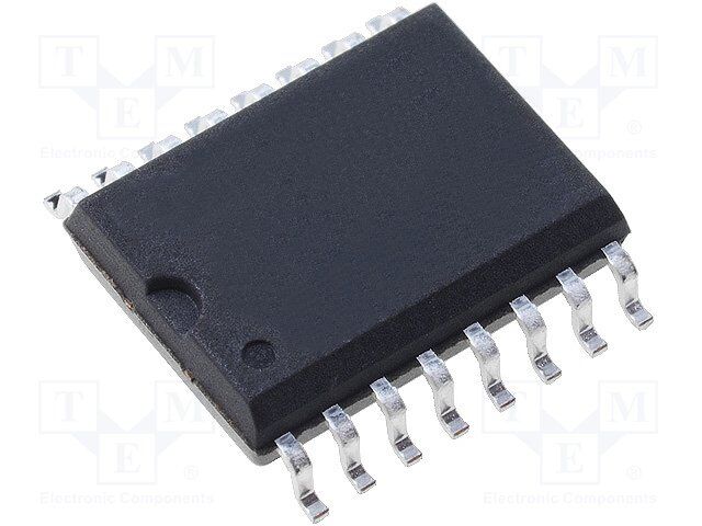
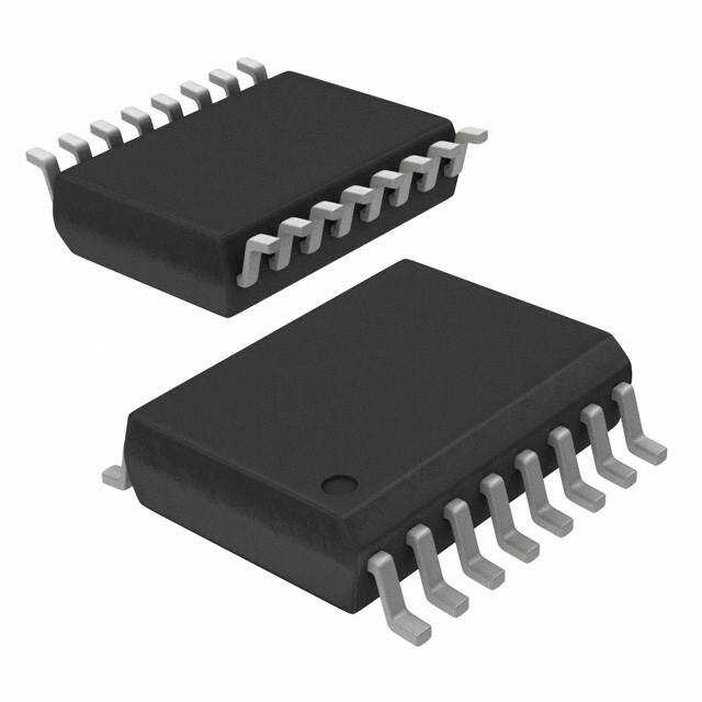
| 描述 | IC DGTL ISO 5CH LOGIC 16SOIC数字隔离器 5-CH Unidirectional Digital |
| 产品分类 | |
| IsolatedPower | 无 |
| 品牌 | Analog Devices |
| 产品手册 | |
| 产品图片 |
|
| rohs | 符合RoHS无铅 / 符合限制有害物质指令(RoHS)规范要求 |
| 产品系列 | 接口 IC,数字隔离器,Analog Devices ADUM1510BRWZiCoupler® |
| 数据手册 | |
| 产品型号 | ADUM1510BRWZ |
| PCN设计/规格 | |
| PulseWidthDistortion(Max) | 5ns |
| 上升/下降时间(典型值) | 2.5ns, 2.5ns |
| 产品目录页面 | |
| 产品种类 | |
| 传播延迟tpLH/tpHL(最大值) | 50ns, 50ns |
| 传播延迟时间 | 50 ns |
| 供应商器件封装 | 16-SOIC W |
| 共模瞬态抗扰度(最小值) | 25kV/µs |
| 其它图纸 |
|
| 包装 | 管件 |
| 商标 | Analog Devices |
| 安装风格 | SMD/SMT |
| 封装 | Tube |
| 封装/外壳 | 16-SOIC(0.295",7.50mm 宽) |
| 封装/箱体 | SOIC-16 |
| 工作温度 | -40°C ~ 105°C |
| 工厂包装数量 | 47 |
| 技术 | 磁耦合 |
| 数据速率 | 10Mbps |
| 最大工作温度 | + 105 C |
| 最大数据速率 | 10 Mb/s |
| 最小工作温度 | - 40 C |
| 标准包装 | 47 |
| 电压-电源 | 4.5 V ~ 5.5 V |
| 电压-隔离 | 2500Vrms |
| 电源电压-最大 | 5.5 V |
| 电源电压-最小 | 4.5 V |
| 电源电流 | 4 mA |
| 类型 | General Purpose |
| 系列 | ADUM1510 |
| 绝缘电压 | 2.5 kVrms |
| 脉宽失真(最大) | 5ns |
| 视频文件 | http://www.digikey.cn/classic/video.aspx?PlayerID=1364138032001&width=640&height=505&videoID=2219593469001http://www.digikey.cn/classic/video.aspx?PlayerID=1364138032001&width=640&height=505&videoID=2219593470001http://www.digikey.cn/classic/video.aspx?PlayerID=1364138032001&width=640&height=505&videoID=2219614223001 |
| 输入-输入侧1/输入侧2 | 5/0 |
| 通道数 | 5 |
| 通道数量 | 5 Channel |
| 通道类型 | 单向 |
| 隔离式电源 | 无 |


- 商务部:美国ITC正式对集成电路等产品启动337调查
- 曝三星4nm工艺存在良率问题 高通将骁龙8 Gen1或转产台积电
- 太阳诱电将投资9.5亿元在常州建新厂生产MLCC 预计2023年完工
- 英特尔发布欧洲新工厂建设计划 深化IDM 2.0 战略
- 台积电先进制程称霸业界 有大客户加持明年业绩稳了
- 达到5530亿美元!SIA预计今年全球半导体销售额将创下新高
- 英特尔拟将自动驾驶子公司Mobileye上市 估值或超500亿美元
- 三星加码芯片和SET,合并消费电子和移动部门,撤换高东真等 CEO
- 三星电子宣布重大人事变动 还合并消费电子和移动部门
- 海关总署:前11个月进口集成电路产品价值2.52万亿元 增长14.8%


PDF Datasheet 数据手册内容提取
5-Channel, Unidirectional Digital Isolator Data Sheet ADuM1510 FEATURES FUNCTIONAL BLOCK DIAGRAM RoHS compliant, 16-lead, wide body SOIC package Low power operation: 5 V VDD1 1 ADuM1510 16VDD2 1.3 mA per channel maximum at 0 Mbps to 2 Mbps GND1 2 15 GND2 VIA 3 ENCODE DECODE 14 VOA 3.3 mA per channel maximum at 10 Mbps High temperature operation: 105°C VIB 4 ENCODE DECODE 13 VOB Up to 10 Mbps data rate (NRZ) VIC 5 ENCODE DECODE 12 VOC (cid:1)(cid:1)(cid:1) default output state VID 6 ENCODE DECODE 11 VOD SaUfeLt yre acnodg rneitgiuolna:t 3o7ry5 0a pVp rrmosv afolsr 1 minute per UL 1577 GNVDIE1 87 ENCODE DECODE 190 VGONED2 06790-001 APPLICATIONS Figure 1. General-purpose, unidirectional, multichannel isolation GENERAL DESCRIPTION The ADuM15101 is a unidirectional, 5-channel isolator based characteristics. The need for external drivers and other discrete on the Analog Devices, Inc., iCoupler® technology. Combining components is eliminated with iCoupler products. In addition, high speed CMOS and monolithic air core transformer technology, iCoupler devices run at one-tenth to one-sixth the power these isolation components provide outstanding performance consumption of optocouplers at comparable signal data rates. characteristics superior to alternatives such as optocoupler devices. The ADuM1510 isolator provides five independent isolation By avoiding the use of LEDs and photodiodes, iCoupler devices channels supporting data rates up to 10 Mbps. The ADuM1510 eliminate the design difficulties commonly associated with operates with the supply voltage of either side ranging from 4.5 V optocouplers. The typical optocoupler concerns regarding to 5.5 V. Unlike other optocoupler alternatives, the ADuM1510 uncertain current transfer ratios, nonlinear transfer functions, isolator has a patented refresh feature that ensures dc correctness in and temperature and lifetime effects are eliminated with the the absence of input logic transitions and during power-up/ simple iCoupler digital interfaces and stable performance power-down conditions. 1 Protected by U.S. Patents 5,952,849; 6,873,065; and 7,075,329. Rev. D Document Feedback Information furnished by Analog Devices is believed to be accurate and reliable. However, no responsibility is assumed by Analog Devices for its use, nor for any infringements of patents or other One Technology Way, P.O. Box 9106, Norwood, MA 02062-9106, U.S.A. rights of third parties that may result from its use. Specifications subject to change without notice. No license is granted by implication or otherwise under any patent or patent rights of Analog Devices. Tel: 781.329.4700 ©2008–2015 Analog Devices, Inc. All rights reserved. Trademarks and registered trademarks are the property of their respective owners. Technical Support www.analog.com
ADuM1510 Data Sheet TABLE OF CONTENTS Features .............................................................................................. 1 ESD Caution...................................................................................5 Applications ....................................................................................... 1 Pin Configuration and Function Descriptions ..............................6 General Description ......................................................................... 1 Typical Performance Characteristics ..............................................7 Functional Block Diagram .............................................................. 1 Applications Information .................................................................8 Revision History ............................................................................... 2 PCB Layout ....................................................................................8 Specifications ..................................................................................... 3 Propagation Delay-Related Parameters ......................................8 Electrical Characteristics—5 V Operation................................ 3 DC Correctness and Magnetic Field Immunity ............................8 Package Characteristics ............................................................... 4 Power Consumption .....................................................................9 Regulatory Information ............................................................... 4 Power-Up/Power-Down Considerations ...................................9 Insulation and Safety-Related Specifications ............................ 4 Outline Dimensions ....................................................................... 11 Recommended Operating Conditions ...................................... 4 Ordering Guide .......................................................................... 11 Absolute Maximum Ratings ............................................................ 5 REVISION HISTORY 10/15—Rev. C to Rev. D Change to Features Section ............................................................. 1 Changes to Table 3 ............................................................................ 4 5/14—Rev. B to Rev. C Changed Double/Reinforced Insulation to Single Protection, Table 3 ................................................................................................ 4 3/12—Rev. A to Rev. B Created Hyperlink for Safety and Regulatory Approvals Entry in Features Section ............................................................................ 1 Change to PCB Layout Section ....................................................... 8 Updated Outline Dimensions ....................................................... 11 9/08—Revision A: Initial Version Rev. D | Page 2 of 12
Data Sheet ADuM1510 SPECIFICATIONS ELECTRICAL CHARACTERISTICS—5 V OPERATION All voltages are relative to their respective ground. 4.5 V ≤ V ≤ 5.5 V, 4.5 V ≤ V ≤ 5.5 V; all minimum/maximum specifications apply DD1 DD2 over the entire recommended operation range, unless otherwise noted; all typical specifications are at T = 25°C, V = V = 5 V. A DD1 DD2 Table 1. Parameter Symbol Min Typ Max Unit Test Conditions/Comments DC SPECIFICATIONS Input Quiescent Supply Current per Channel I 0.40 0.80 mA DDI (Q) Output Quiescent Supply Current per Channel I 0.30 0.50 mA DDO (Q) Total Supply Current, Five Channels1 V Supply Current, Quiescent I 2.0 4.0 mA V = V = V = V = V = 0 V DD1 DD1 (Q) IA IB IC ID IE V Supply Current, Quiescent I 1.5 2.5 mA V = V = V = V = V = 0 V DD2 DD2 (Q) IA IB IC ID IE V Supply Current, 10 Mbps Data Rate I 7.5 12.0 mA 5 MHz logic signal frequency DD1 DD1 (10) V Supply Current, 10 Mbps Data Rate I 3.1 4.5 mA 5 MHz logic signal frequency DD2 DD2 (10) Input Currents I , I , I , I , I −10 +1 +10 µA V , V , V , V , V ≥ 0 V IA IB IC ID IE IA IB IC ID IE Logic High Input Threshold V 2.0 V IH Logic Low Input Threshold V 0.8 V IL Logic High Output Voltages V , V , V − 0.4 4.8 V I = −4 mA, V = V OAH OBH DD2 Ox Ix IH V , V , OCH ODH V OEH Logic Low Output Voltages V , V , 0.2 0.4 V I = +4 mA, V = V OAL OBL Ox Ix IL V , V , V OCL ODL OEL SWITCHING SPECIFICATIONS Minimum Pulse Width2 PW 100 ns C = 15 pF, CMOS signal levels L Maximum Data Rate3 10 Mbps C = 15 pF, CMOS signal levels L Propagation Delay4 t , t 20 30 50 ns C = 15 pF, CMOS signal levels PHL PLH L Pulse Width Distortion, |t − t |4 PWD 5 ns C = 15 pF, CMOS signal levels PLH PHL L Change vs. Temperature 5 ps/°C C = 15 pF, CMOS signal levels L Propagation Delay Skew5 t 30 ns C = 15 pF, CMOS signal levels PSK L Channel-to-Channel Matching6 t 5 ns C = 15 pF, CMOS signal levels PSKCD L Output Rise/Fall Time (10% to 90%) t/t 2.5 ns C = 15 pF, CMOS signal levels R F L Common-Mode Transient Immunity at |CM | 25 35 kV/µs V = V /V , V = 1000 V, H Ix DD1 DD2 CM Logic High Output7 transient magnitude = 800 V Common-Mode Transient Immunity at |CM| 25 35 kV/µs V = 0 V, V = 1000 V, L Ix CM Logic Low Output7 transient magnitude = 800 V Refresh Rate f 1.0 Mbps r Input Dynamic Supply Current per Channel8 I 0.122 mA/Mbps DDI (D) Output Dynamic Supply Current per Channel8 I 0.036 mA/Mbps DDO (D) 1 Supply current values are for all five channels combined running at identical data rates. Output supply current values are specified with no output load present. The supply current associated with an individual channel operating at a given data rate is calculated as described in the Power Consumption section. See Figure 4 through Figure 6 for information on the per-channel supply current as a function of the data rate for unloaded and loaded conditions. See Figure 7 and Figure 8 for total IDD1 and IDD2 supply currents as a function of the data rate for the ADuM1510. 2 The minimum pulse width is the shortest pulse width at which the specified pulse width distortion is guaranteed. Operation below the minimum pulse width is not recommended. 3 The maximum data rate is the fastest data rate at which the specified pulse width distortion is guaranteed. 4 tPHL propagation delay is measured from the 50% level of the falling edge of the VIx signal to the 50% level of the falling edge of the VOx signal. tPLH propagation delay is measured from the 50% level of the rising edge of the VIx signal to the 50% level of the rising edge of the VOx signal. 5 tPSK is the magnitude of the worst-case difference in tPHL and/or tPLH that is measured between units at the same operating temperature, supply voltages, and output load within the recommended operating conditions. 6 Channel-to-channel matching is the absolute value of the difference in propagation delays between any two channels within the same component. 7 CMH is the maximum common-mode voltage slew rate that can be sustained while maintaining VOx > 0.8 × VDD2. CML is the maximum common-mode voltage slew rate that can be sustained while maintaining VOx < 0.8 V. The common-mode voltage slew rates apply to both rising and falling common-mode voltage edges. The transient magnitude is the range over which the common mode is slewed. 8 Dynamic supply current is the incremental amount of supply current required for a 1 Mbps increase in the signal data rate. See Figure 4 through Figure 6 for infor- mation on the per-channel supply current as a function of the data rate for unloaded and loaded conditions. See the Power Consumption section for guidance on calculating the per-channel supply current for a given data rate. Rev. D | Page 3 of 12
ADuM1510 Data Sheet PACKAGE CHARACTERISTICS Table 2. Parameter Symbol Min Typ Max Unit Test Conditions/Comments Resistance (Input-to-Output)1 R 1012 Ω I-O Capacitance (Input-to-Output)2 C 2.2 pF f = 1 MHz I-O Input Capacitance2 C 4.0 pF I IC Junction-to-Case Thermal Resistance, Side 1 θ 33 °C/W Thermocouple located at center of JCI package underside IC Junction-to-Case Thermal Resistance, Side 2 θ 28 °C/W Thermocouple located at center of JCO package underside 1 The device is considered a two-terminal device. Pin 1 through Pin 8 are shorted together, and Pin 9 through Pin 16 are shorted together. 2 Input capacitance is from any input data pin to ground. REGULATORY INFORMATION The ADuM1510 has been approved by the following organization upon product release, as shown in Table 3. Table 3. UL Recognized under UL 1577 Component Recognition Program1 Single protection, 3750 V rms isolation voltage File E214100 1 In accordance with UL 1577, each ADuM1510 is proof-tested by applying an insulation test voltage ≥ 4500 V rms for 1 sec (current leakage detection limit > 7.5 µA). INSULATION AND SAFETY-RELATED SPECIFICATIONS Table 4. Parameter Symbol Value Unit Test Conditions/Comments Rated Dielectric Insulation Voltage 2500 V rms 1 minute duration Minimum External Air Gap (Clearance) L(I01) 7.7 min mm Measured from input terminals to output terminals, shortest distance through air Minimum External Tracking (Creepage) L(I02) 8.1 min mm Measured from input terminals to output terminals, shortest distance path along body Minimum Internal Gap (Internal Clearance) 0.017 min mm Insulation distance through insulation. Tracking Resistance (Comparative Tracking Index) CTI >175 V DIN IEC 112/VDE 0303 Part 1 Isolation Group IIIa Material Group (DIN VDE 0110, 1/89, Table 1) Maximum Working Voltage Compatible with 50 Years V 565 V peak Continuous peak voltage across the isolation IORM Service Life barrier RECOMMENDED OPERATING CONDITIONS All voltages are relative to their respective ground. See the DC Correctness and Magnetic Field Immunity section for information on immunity to external magnetic fields. Table 5. Parameter Symbol Min Typ Max Unit Operating Temperature T −40 +105 °C A Supply Voltages V , V 4.5 5.5 V DD1 DD2 Input Signal Rise and Fall Times 1.0 ms Rev. D | Page 4 of 12
Data Sheet ADuM1510 ABSOLUTE MAXIMUM RATINGS Ambient temperature T = 25°C, unless otherwise noted. A Stresses at or above those listed under Absolute Maximum Ratings may cause permanent damage to the product. This is a Table 6. stress rating only; functional operation of the product at these Parameter Rating or any other conditions above those indicated in the operational Storage Temperature (T ) Range −65°C to +150°C ST section of this specification is not implied. Operation beyond Ambient Operating Temperature (T ) −40°C to +105°C A the maximum operating conditions for extended periods may Range affect product reliability. Supply Voltages1 (V , V ) −0.5 V to +7.0 V DD1 DD2 Input Voltages1 (VIA, VIB, VIC, VID, VIE) −0.5 V to VDDI + 0.5 V Output Voltages1 (V , V , V , V , V ) −0.5 V to V + 0.5 V OA OB OC OD OE DDO ESD CAUTION Average Output Current per Pin2 Side 1 (I ) −18 mA to +18 mA O1 Side 2 (I ) −22 mA to +22 mA O2 Common-Mode Transients3 −100 kV/μs to +100 kV/μs 1 All voltages are relative to their respective ground. 2 See Figure 3 for maximum rated current values for various temperatures. 3 Refers to common-mode transients across the insulation barrier. Common- mode transients exceeding the absolute maximum ratings may cause latch- up or permanent damage. Rev. D | Page 5 of 12
ADuM1510 Data Sheet PIN CONFIGURATION AND FUNCTION DESCRIPTIONS VDD1 1 16 VDD2 GND1* 2 15 GND2* VIA 3 ADuM1510 14 VOA VIB 4 TOP VIEW 13 VOB VIC 5 (Not to Scale) 12 VOC VID 6 11 VOD VIE 7 10 VOE GND1* 8 9 GND2* *PIN 2 AND PIN 8 ARE INTERNALLY CONNECTED. CONNECTING BOTH TCOO NGNNEDC1T IESD R. ECCOONMNMEECNTIDNEGD B. POITNH 9 TAON DG NPDIN2 1IS5 RAERCEO INMTMEERNNDAELDL.Y 06790-002 Figure 2. Pin Configuration Table 7. Pin Function Descriptions Pin No. Mnemonic Description 1 V Supply Voltage for Isolator Side 1 (4.5 V to 5.5 V). DD1 2, 8 GND Ground 1. Ground reference for Isolator Side 1. Pin 2 and Pin 8 are internally connected, and connecting both to 1 GND is recommended. 1 3 V Logic Input A. IA 4 V Logic Input B. IB 5 V Logic Input C. IC 6 V Logic Input D. ID 7 V Logic Input E. IE 9, 15 GND Ground 2. Ground reference for Isolator Side 2. Pin 9 and Pin 15 are internally connected, and connecting both to 2 GND is recommended. 2 10 V Logic Output E. OE 11 V Logic Output D. OD 12 V Logic Output C. OC 13 V Logic Output B. OB 14 V Logic Output A. OA 16 V Supply Voltage for Isolator Side 2 (4.5 V to 5.5 V). DD2 Table 8. Truth Table (Positive Logic) V V V V Ix DD1 DD2 Ox Input1 State State Output1 Description H Powered Powered H Normal operation, data is high. L Powered Powered L Normal operation, data is low. X Unpowered Powered L Input unpowered. Outputs return to input state within 1 μs of V power restoration. DD1 See the Power-Up/Power-Down Considerations section for more details. X Powered Unpowered Z Output unpowered. Output pins are in high impedance state. Outputs return to input state within 1 μs of V power restoration. See the Power-Up/Power-Down DD2 Considerations section for more details. 1 VIx and VOx refer to the input and output signals of a given channel (A, B, C, D, or E). Rev. D | Page 6 of 12
Data Sheet ADuM1510 TYPICAL PERFORMANCE CHARACTERISTICS 350 1.6 300 mA) 1.4 A) D ( T (m 250 LOA 1.2 REN SIDE 2 5pF 1.0 G CUR 200 NEL, 1 0.8 N N MITI 150 SIDE 1 CHA 0.6 LI T/ AFETY- 100 URREN 0.4 S 50 CD2 0.2 D V 00 50 CASE TEMP1E0R0ATURE (°C)150 200 06790-003 00 2 DA4TA RATE (Mb6ps) 8 10 06790-006 Figure 3. Thermal Derating Curve, Dependence of Safety-Limiting Values Figure 6. Typical Output Supply Current per Channel vs. Data Rate with Case Temperature per DIN V VDE V 0884-10 (15 pF Output Load) 1.6 8 1.4 7 mA) 1.2 6 NEL ( 1.0 mA) 5 NT/CHAN 0.8 URRENT ( 4 CURRE 0.6 V CDD1 3 D1 0.4 2 D V 0.2 1 00 2 DA4TA RATE (Mb6ps) 8 10 06790-004 00 2 DA4TA RATE (Mb6ps) 8 10 06790-007 Figure 4. Typical Input Supply Current per Channel vs. Data Rate Figure 7. Typical Total VDD1 Supply Current vs. Data Rate 1.6 8 1.4 7 ANNEL (mA) 11..20 F LOAD (mA) 65 V CURRENT/CHDD2 000...864 V CURRENT, 15pDD2 432 0.2 1 00 2 DA4TA RATE (Mb6ps) 8 10 06790-005 00 2 DAT4A RATE (Mb6ps) 8 10 06790-008 Figure 5. Typical Output Supply Current per Channel vs. Data Rate Figure 8. Typical Total VDD2 Supply Current vs. Data Rate (No Output Load) (15 pF Output Load) Rev. D | Page 7 of 12
ADuM1510 Data Sheet APPLICATIONS INFORMATION PCB LAYOUT If the decoder receives no pulses for more than approximately 5 μs, the input side is assumed to be unpowered or nonfunctional, in The ADuM1510 digital isolator requires no external interface which case, the isolator output is forced to a default low state by circuitry for the logic interfaces. Power supply bypassing is the watchdog timer circuit (see Table 8). strongly recommended at the input and output supply pins (see Figure 9). Bypass capacitors are most conveniently connected The limitation on the magnetic field immunity of the device is between Pin 1 and Pin 2 for V and between Pin 15 and Pin 16 set by the condition in which induced voltage in the transformer DD1 for V . The capacitor value should be between 0.01 μF and receiving coil is sufficiently large to either falsely set or reset the DD2 0.1 μF. The total lead length between both ends of the capacitor decoder. The analysis below defines such conditions. In the follow- and the input power supply pin must not exceed 10 mm. Bypassing ing analysis, the ADuM1510 is examined in a 3 V operating between Pin 1 and Pin 8 and between Pin 9 and Pin 16 should condition because it represents the most susceptible mode of also be considered unless the ground pair on each package side operation of all products in its product family. is connected close to the package. The pulses at the transformer output have an amplitude greater VDD1 VDD2 than 1.0 V. The decoder has a sensing threshold of approximately GND1 GND2 0.5 V, thus establishing a 0.5 V margin in which induced voltages VIA VOA VIB ADuM1510 VOB can be tolerated. The voltage induced across the receiving coil is VIC VOC given by VID VOD GNVDIE1 VGONED2 06790-009 V = (−dβ/dt) Σπrn2; n = 1, 2, … N Figure 9. Recommended PCB Layout where: See the AN-1109 Application Note for board layout guidelines. β is the magnetic flux density (gauss). r is the radius of the nth turn in the receiving coil (cm). PROPAGATION DELAY-RELATED PARAMETERS n N is the number of turns in the receiving coil. Propagation delay is a parameter that describes the length of Given the geometry of the receiving coil in the ADuM1510 and time it takes for a logic signal to propagate through a component. an imposed requirement that the induced voltage be at most The propagation delay to a logic low output can differ from the 50% of the 0.5 V margin at the decoder, a maximum allowable propagation delay to a logic high output. magnetic field can be calculated, as shown in Figure 11. INPUT (VIx) 50% 100 X tPLH tPHL LU F OUTPUT (VOx) Figure 10. Propagation Delay Parameters5 0% 06790-010 AGNETIC ss) 10 Mu 1 E ga Pulse width distortion is the maximum difference between ABLY (k tahcecsuer atwteoly p trhoep taimgaitniogn o df ethlaey ivnapluute ss iagnnda li sis a pnr einsedrivceatdi.o n of how ALLOWDENSIT0.1 M Channel-to-channel matching refers to the maximum amount U M 0.01 that the propagation delay differs between channels within a AXI M single ADuM1510 component. Pthreo pparogaptaigoant idoenla dye slakye wd irfefefersr sa tmo otnhge mmauxltiimpluem A DamuMou1n5t1 t0h at 0.0011k 10kMAGNETI1C0 0FkIELD FREQ1MUENCY (Hz1)0M 100M 06790-011 Figure 11. Maximum Allowable External Magnetic Flux Density components operated under the same conditions. For example, at a magnetic field frequency of 1 MHz, the DC CORRECTNESS AND MAGNETIC FIELD IMMUNITY maximum allowable magnetic field of 0.2 kgauss induces a Positive and negative logic transitions at the isolator input cause voltage of 0.25 V at the receiving coil. This voltage is approximately narrow (~1 ns) pulses to be sent via the transformer to the decoder. 50% of the sensing threshold and does not cause a faulty output The decoder is bistable and is, therefore, either set or reset by transition. Similarly, if such an event occurs during a transmitted the pulses indicating input logic transitions. In the absence of pulse (and is of the worst-case polarity), the received pulse is logic transitions at the input for more than ~1 μs, a periodic set reduced from >1.0 V to 0.75 V, still well above the 0.5 V sensing of refresh pulses indicative of the correct input state is sent to threshold of the decoder. ensure dc correctness at the output. Rev. D | Page 8 of 12
Data Sheet ADuM1510 The preceding magnetic flux density values correspond to To calculate the total I and I supply current, the supply DD1 DD2 specific current magnitudes at given distances away from the currents for each input and output channel corresponding to ADuM1510 transformers. Figure 12 expresses these allowable I and I are calculated and totaled. Figure 4 and Figure 5 DD1 DD2 current magnitudes as a function of frequency for selected provide per-channel supply currents as a function of the data distances. As seen in Figure 12, the ADuM1510 is extremely rate for an unloaded output condition. Figure 6 provides per- immune and is affected only by extremely large currents channel supply current as a function of the data rate for a 15 pF operated at high frequency and very close to the component. output condition. Figure 7 and Figure 8 provide total I and DD1 For example, at a magnetic field frequency of 1 MHz, a 0.5 kA I supply current as a function of the data rate for ADuM1510 DD2 current would need to be placed 5 mm away from the products. ADuM1510 to affect the operation of the component. POWER-UP/POWER-DOWN CONSIDERATIONS 1000 Given that the ADuM1510 has separate supplies on each side of DISTANCE = 1m A) the isolation barrier, the power-up and power-down characteristics k T ( 100 relative to each supply voltage need to be considered individually. N E R R As shown in Table 8, when V input power is off, the ADuM1510 U DD1 C LE 10 outputs take on a default low logic condition. As the VDD1 supply AB DISTANCE = 100mm is increased or decreased, the output of each channel transitions W O from/to the default condition to/from the state matching its L 1 L A respective signals (see Figure 13 and Figure 14). M DISTANCE = 5mm U M OUTPUT XI 0.1 DATA A M 0.01 1k 10MkAGNET1IC0 0FkIELD FRE1QMUENCY (H1z0)M 100M 06790-012 2V VDD1 Figure 12. Maximum Allowable Current for (TYP) Note that at comVabriinouast iCounrrse ontf- tsotr-AoDnugM m15a1g0n Septaicc ifnigesl d and high 06790-013 frequency, any loops formed by PCB traces can induce sufficiently Figure 13. VDD1 Power-Up/Power-Down Characteristics, Input Data = High large error voltages to trigger the thresholds of succeeding circuitry. Take care in the layout of such traces to avoid this possibility. VDD1 POWER CONSUMPTION The supply current at a given channel of the ADuM1510 idsaotlaa troart ei,s aan fdu nthceti cohna onfn tehl eo suutpppulty l ovaodlt.a ge, the channel OUTPUT DATA 06790-014 Figure 14. VDD1 Power-Up/Power-Down Characteristics, Input Data = Low For each input channel, the supply current is given by When V crosses the threshold for activating the refresh circuit DD1 I = I f ≤ 0.5f DDI DDI (Q) r (approximately 2 V), there can be a delay of up to 2 μs before the I = I × (2f − f) + I f > 0.5f output is updated to the correct state, depending on the timing DDI DDI (D) r DDI (Q) r of the next refresh pulse. When V is reduced from an on state For each output channel, the supply current is given by DD1 below the 2 V threshold, there can be a delay of up to 5 μs before I = I f ≤ 0.5f DDO DDO (Q) r the output takes on its default low state. This corresponds to the I = (I + CV ) × (2f − f) + I f ≤ 0.5f duration that the watchdog timer circuit at the input is designed DDO DDO (D) L DDO r DDO (Q) r to wait before triggering an output default state. where: IDDI (Q), IDDO (Q) are the specified input and output quiescent When the VDD2 output supply is below the level at which the supply currents (mA). ADuM1510 output transistors are biased (approximately 1 V), I , I are the input and output dynamic supply currents the outputs take on a high impedance state. DDI (D) DDO (D) per channel (mA/Mbps). C is the output load capacitance (pF). L V is the output supply voltage (V). DDO f is the input logic signal frequency (MHz, half of the input data rate, NRZ signaling). f is the input stage refresh rate (Mbps). r Rev. D | Page 9 of 12
ADuM1510 Data Sheet When V is above a value of approximately 2 V, each channel DD2 OUTPUT LOW output takes on a state matching that of its respective input. T T T T UZ U U UZ Between the values of 1 V and 2 V, the outputs are set low. This OUTPHIGH- OUTPLOW OUTPLOW OUTPHIGH- behavior is shown in Figure 15 and Figure 16. ~2V OUTPUT HIGH ~1V OUTPUTHIGH-Z OUTPUTLOW OUTPUTLOW OUTPUTHIGH-Z Figure 16. VDD2V PDDo2wer-Up/Power-Down Characteristics, InpuVDtD D2ata = Lo06790-016w ~2V ~1V VDD2 VDD2 06790-015 Figure 15. VDD2 Power-Up/Power-Down Characteristics, Input Data = High Rev. D | Page 10 of 12
Data Sheet ADuM1510 OUTLINE DIMENSIONS 10.50(0.4134) 10.10(0.3976) 16 9 7.60(0.2992) 7.40(0.2913) 1 8 10.65(0.4193) 10.00(0.3937) 1.27(0.0500) 0.75(0.0295) BSC 2.65(0.1043) 0.25(0.0098) 45° 0.30(0.0118) 2.35(0.0925) 8° 0.10(0.0039) 0° COPLANARITY 0.10 0.51(0.0201) SPELAATNIENG 0.33(0.0130) 1.27(0.0500) 0.31(0.0122) 0.20(0.0079) 0.40(0.0157) C(RINOEFNPEATRRREOENNLCLTEIHNCEOGOSNDMELISPYM)LAEAIANNRNDSETIAORTRNOOESUJNANEORDDETEEDAICN-POSMPFTRIFALONLMPIDMIRLAELIRATIMTDEEESRTFSMEO;SRIRN-0ECU1QH3SU-EADIVAIINMAELDENENSSTIIOGSNNFS.OR 03-27-2007-B Figure 17. 16-Lead Standard Small Outline Package [SOIC_W] Wide Body (RW-16) Dimensions shown in millimeters and (inches) ORDERING GUIDE Number Number Maximum Maximum Maximum of Inputs, of Inputs, Data Rate Propagation Pulse Width Temperature Package Package Model1 V Side V Side (Mbps) Delay, 5 V (ns) Distortion (ns) Range Description Option DD1 DD2 ADuM1510BRWZ 5 0 10 50 5 −40°C to +105°C 16-Lead SOIC_W RW-16 ADuM1510BRWZ-RL 5 0 10 50 5 −40°C to +105°C 16-Lead SOIC_W, RW-16 13” Tape and Reel 1 Z = RoHS Compliant Part. Rev. D | Page 11 of 12
ADuM1510 Data Sheet NOTES ©2008–2015 Analog Devices, Inc. All rights reserved. Trademarks and registered trademarks are the property of their respective owners. D06790-0-10/15(D) Rev. D | Page 12 of 12