 Datasheet下载
- 型号: ADUM1310ARWZ-RL
- 制造商: Analog
- 库位|库存: xxxx|xxxx
- 要求:
| 数量阶梯 | 香港交货 | 国内含税 |
| +xxxx | $xxxx | ¥xxxx |
查看当月历史价格
查看今年历史价格
ADUM1310ARWZ-RL产品简介:
ICGOO电子元器件商城为您提供ADUM1310ARWZ-RL由Analog设计生产,在icgoo商城现货销售,并且可以通过原厂、代理商等渠道进行代购。 ADUM1310ARWZ-RL价格参考。AnalogADUM1310ARWZ-RL封装/规格:数字隔离器, 通用 数字隔离器 3750Vrms 3 通道 1Mbps 25kV/µs CMTI 16-SOIC(0.295",7.50mm 宽)。您可以下载ADUM1310ARWZ-RL参考资料、Datasheet数据手册功能说明书,资料中有ADUM1310ARWZ-RL 详细功能的应用电路图电压和使用方法及教程。
ADUM1310ARWZ-RL 是由 Analog Devices Inc.(现为 ADI,亚德诺半导体)生产的一款数字隔离器,属于 iCoupler 系列。该型号采用 ADI 的芯片级变压器技术,提供高可靠性、低功耗和高速度的信号隔离能力。以下是其主要应用场景:

 1. 工业自动化与控制
   - PLC 和 I/O 模块:用于可编程逻辑控制器(PLC)中的输入/输出模块,实现信号隔离以防止噪声干扰。
   - 电机驱动器:在工业电机控制系统中,隔离控制信号以保护敏感电路。
   - 传感器接口:将工业传感器的信号与主控系统隔离,确保数据传输的稳定性和安全性。

 2. 通信设备
   - RS-485/RS-422 接口:在长距离通信中,隔离收发器与主机之间的信号,避免地电位差引起的损坏。
   - 光纤通信:在光模块或光纤收发器中,隔离数字信号以提高抗干扰能力。

 3. 医疗设备
   - 患者监护仪:如心电图(ECG)设备中,隔离患者信号与设备内部电路,确保患者安全。
   - 便携式医疗设备:在低功耗要求下,提供可靠的信号隔离功能。

 4. 汽车电子
   - 车载网络:在 CAN 总线或 LIN 总线系统中,隔离节点间的通信信号,增强系统的抗噪能力。
   - 电池管理系统 (BMS):在电动汽车中,隔离电池监控信号以保护核心控制单元。

 5. 消费类电子产品
   - 电源适配器:在开关电源中隔离反馈信号,提高电源的安全性。
   - 家用自动化设备:如智能插座或智能家居控制器,实现信号隔离以防止电磁干扰。

 特点总结
- 高隔离电压:支持高达 2.5 kVrms 的隔离电压,适用于严苛环境。
- 低功耗:适合对能效要求较高的应用。
- 宽工作温度范围:-40°C 至 +125°C,适应各种工业和户外场景。
- 小型封装:SOIC_W 宽体封装,节省空间且易于集成。

ADUM1310ARWZ-RL 的高性能和灵活性使其成为需要可靠信号隔离的各种应用的理想选择。
| 参数 | 数值 |
| 产品目录 | |
| ChannelType | 单向 |
| 描述 | IC DGTL ISO 3CH LOGIC 16SOIC |
| 产品分类 | |
| IsolatedPower | 无 |
| 品牌 | Analog Devices Inc |
| 数据手册 | |
| 产品图片 |
|
| 产品型号 | ADUM1310ARWZ-RL |
| PCN设计/规格 | |
| PulseWidthDistortion(Max) | 40ns |
| rohs | 无铅 / 符合限制有害物质指令(RoHS)规范要求 |
| 产品系列 | iCoupler® |
| 上升/下降时间(典型值) | 2.5ns, 2.5ns |
| 传播延迟tpLH/tpHL(最大值) | 100ns, 100ns |
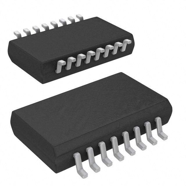
| 供应商器件封装 | 16-SOIC |
| 共模瞬态抗扰度(最小值) | 25kV/µs |
| 其它名称 | ADUM1310ARWZ-RLDKR |
| 包装 | Digi-Reel® |
| 封装/外壳 | 16-SOIC(0.295",7.50mm 宽) |
| 工作温度 | -40°C ~ 105°C |
| 技术 | 磁耦合 |
| 数据速率 | 1Mbps |
| 标准包装 | 1 |
| 电压-电源 | 2.7 V ~ 5.5 V |
| 电压-隔离 | 2500Vrms |
| 类型 | 通用 |
| 脉宽失真(最大) | 40ns |
| 视频文件 | http://www.digikey.cn/classic/video.aspx?PlayerID=1364138032001&width=640&height=505&videoID=2219593469001http://www.digikey.cn/classic/video.aspx?PlayerID=1364138032001&width=640&height=505&videoID=2219593470001http://www.digikey.cn/classic/video.aspx?PlayerID=1364138032001&width=640&height=505&videoID=2219614223001 |
| 输入-输入侧1/输入侧2 | 3/0 |
| 通道数 | 3 |
| 通道类型 | 单向 |
| 隔离式电源 | 无 |


- 商务部:美国ITC正式对集成电路等产品启动337调查
- 曝三星4nm工艺存在良率问题 高通将骁龙8 Gen1或转产台积电
- 太阳诱电将投资9.5亿元在常州建新厂生产MLCC 预计2023年完工
- 英特尔发布欧洲新工厂建设计划 深化IDM 2.0 战略
- 台积电先进制程称霸业界 有大客户加持明年业绩稳了
- 达到5530亿美元!SIA预计今年全球半导体销售额将创下新高
- 英特尔拟将自动驾驶子公司Mobileye上市 估值或超500亿美元
- 三星加码芯片和SET,合并消费电子和移动部门,撤换高东真等 CEO
- 三星电子宣布重大人事变动 还合并消费电子和移动部门
- 海关总署:前11个月进口集成电路产品价值2.52万亿元 增长14.8%


PDF Datasheet 数据手册内容提取
Triple-Channel Digital Isolators Data Sheet ADuM1310/ADuM1311 FEATURES FUNCTIONAL BLOCK DIAGRAMS Low power operation VDD1 1 ADuM1310 16 VDD2 5 V operation 1.7 mA per channel maximum at 0 Mbps to 2 Mbps GND1 2 15 GND2 4.0 mA per channel maximum at 2 Mbps to 10 Mbps VIA 3 ENCODE DECODE 14 VOA 3 V operation 1.0 mA per channel maximum at 0 Mbps to 2 Mbps VIB 4 ENCODE DECODE 13 VOB 2.1 mA per channel maximum at 2 Mbps to 10 Mbps VIC 5 ENCODE DECODE 12 VOC Bidirectional communication 3 V/5 V level translation NC 6 11 NC Schmitt trigger inputs DISABLE 7 10 CTRL2 High temperature operation: 105°C Up to 10 Mbps data rate (NRZ) GND1 8 9 GND2 04904-001 Programmable default output state Figure 1. ADuM1310 High common-mode transient immunity: >25 kV/μs 16-lead, RoHS-compliant, SOIC wide body package VDD1 1 ADuM1311 16 VDD2 8.1 mm external creepage Safety and regulatory approvals GND1 2 15 GND2 UL recognition: 3750 V rms for 1 minute per UL 1577 VIA 3 ENCODE DECODE 14 VOA CSA Component Acceptance Notice 5A VDE certificate of conformity VIB 4 ENCODE DECODE 13 VOB DIN V VDE V 0884-10 (VDE V 0884-10): 2006-12 VOC 5 DECODE ENCODE 12 VIC V = 560 V peak working voltage IORM NC 6 11 NC APPLICATIONS CTRL1 7 10 CTRL2 GSPeIn ienrtaelr-fpaucrep/doaseta m counltvicehratenrn ieslo ilsaotiloatni on GND1 8 9 GND2 04904-002 RS-232/RS-422/RS-485 transceiver Figure 2. ADuM1311 Industrial field bus isolation GENERAL DESCRIPTION The ADuM1310/ADuM13111 are 3-channel digital isolators comparable signal data rates. The iCoupler also offers higher based on Analog Devices, Inc., iCoupler® technology. Combin- channel densities and more options for channel directionality. ing high speed CMOS and monolithic air core transformer The ADuM1310/ADuM1311 isolators provide three technology, these isolation components provide outstanding independent isolation channels in a variety of channel performance characteristics superior to alternatives such as configurations and data rates up to 10 Mbps (see the Ordering optocoupler devices. Guide). All models operate with the supply voltage on either By avoiding the use of LEDs and photodiodes, iCoupler devices side ranging from 2.7 V to 5.5 V, providing compatibility with remove the design difficulties commonly associated with opto- lower voltage systems as well as enabling voltage translation couplers. The typical optocoupler concerns regarding uncertain functionality across the isolation barrier. All products allow the current transfer ratios, maximum operating temperature, and user to predetermine the default output state in the absence of input lifetime effects are eliminated with the simple iCoupler digital V power with a simple control pin. Unlike other optocoupler DD1 interfaces and stable performance characteristics. The need for alternatives, the ADuM1310/ADuM1311 isolators have a patented external drivers and other discrete components is eliminated refresh feature that ensures dc correctness in the absence of input with these iCoupler products. Furthermore, iCoupler devices logic transitions and during power-up/ power-down conditions. consume one-tenth to one-sixth the power of optocouplers at 1 Protected by U.S. Patents 5,952,849; 6,873,065; 6,903,578; and 7,075,329. Other patents pending. Rev. K Document Feedback Information furnished by Analog Devices is believed to be accurate and reliable. However, no responsibility is assumed by Analog Devices for its use, nor for any infringements of patents or other One Technology Way, P.O. Box 9106, Norwood, MA 02062-9106, U.S.A. rliicgehntsse o ifs t hgirradn pteadrt bieys itmhaptl micaatyio rne sourl to ftrhoemrw itiss ue suen. Sdpeer caifnicya ptiaotnesn st uobr jpecatt eton tc hriagnhgtse owf iAthnoaulot gn oDteicvei.c Neso. Tel: 781.329.4700 ©2005–2015 Analog Devices, Inc. All rights reserved. Trademarks and registered trademarks are the property of their respective owners. Technical Support www.analog.com
ADuM1310/ADuM1311 Data Sheet TABLE OF CONTENTS Features .............................................................................................. 1 Recommended Operating Conditions .................................... 11 Applications ....................................................................................... 1 Absolute Maximum Ratings ......................................................... 12 Functional Block Diagrams ............................................................. 1 ESD Caution................................................................................ 12 General Description ......................................................................... 1 Pin Configurations and Function Descriptions ......................... 13 Revision History ............................................................................... 2 Typical Performance Characteristics ........................................... 16 Specifications ..................................................................................... 3 Applications Information .............................................................. 18 Electrical Characteristics—5 V Operation................................ 3 PC Board Layout ........................................................................ 18 Electrical Characteristics—3 V Operation................................ 5 Propagation Delay-Related Parameters ................................... 18 Electrical Characteristics—Mixed 5 V/3 V or 3 V/5 V DC Correctness and Magnetic Field Immunity ..................... 18 Operation ....................................................................................... 7 Power Consumption .................................................................. 19 Package Characteristics ............................................................. 10 Insulation Lifetime ..................................................................... 20 Regulatory Information ............................................................. 10 Outline Dimensions ....................................................................... 21 Insulation and Safety-Related Specifications .......................... 10 Ordering Guide .......................................................................... 21 DIN V VDE V 0884-10 (VDE V 0884-10): 2006-12 Insulation Characteristics .......................................................... 11 REVISION HISTORY 6/15—Rev. J to Rev. K 1/07—Rev. E to Rev. F Changes to Table 5 and Table 6 ..................................................... 10 Added ADuM1311 ............................................................. Universal Changes to Typical Performance Characteristics Section ........ 16 Changes to Ordering Guide .......................................................... 20 9/14—Rev. I to Rev. J Changes to Features Section............................................................ 1 10/06—Rev. D to Rev. E Changes to Table 5 and Table 6 ..................................................... 10 Removed ADuM1410 ........................................................ Universal Updated Format .................................................................. Universal 4/14—Rev. H to Rev. I Change to Figure 3 ......................................................................... 10 Change to Table 5 ........................................................................... 10 Changes to Table 10 ....................................................................... 10 Changes to Application Information Section ............................. 12 Updated Outline Dimensions ....................................................... 18 3/12—Rev. G to Rev. H Changes to Ordering Guide .......................................................... 18 Created Hyperlink for Safety and Regulatory Approvals Entry in Features Section ................................................................. 1 3/06—Rev. C to Rev. D Change to PC Board Layout Section ............................................ 18 Updated Outline Dimensions ....................................................... 21 Added Note 1; Changes to Figure 2 ................................................ 1 Changes to Absolute Maximum Ratings ..................................... 11 6/07—Rev. F to Rev. G 11/05—Revision C: Initial Version Updated VDE Certification Throughout ...................................... 1 Changes to Features and Applications ........................................... 1 Changes to DC Specifications in Table 1 ....................................... 3 Changes to DC Specifications in Table 2 ....................................... 5 Changes to DC Specifications in Table 3 ....................................... 7 Changes to Regulatory Information Section .............................. 10 Added Table 10 ............................................................................... 12 Added Insulation Lifetime Section .............................................. 19 Rev. K | Page 2 of 24
Data Sheet ADuM1310/ADuM1311 SPECIFICATIONS ELECTRICAL CHARACTERISTICS—5 V OPERATION 4.5 V ≤ V ≤ 5.5 V, 4.5 V ≤ V ≤ 5.5 V; all minimum/maximum specifications apply over the entire recommended operation range, DD1 DD2 unless otherwise noted; all typical specifications are at T = 25°C, V = V = 5 V. All voltages are relative to their respective grounds. A DD1 DD2 Table 1. Parameter Symbol Min Typ Max Unit Test Conditions/Comments DC SPECIFICATIONS ADuM1310, Total Supply Current, Three Channels1 DC to 2 Mbps V Supply Current I 2.4 3.2 mA DC to 1 MHz logic signal DD1 DD1 (Q) frequency V Supply Current I 1.2 1.6 mA DC to 1 MHz logic signal DD2 DD2 (Q) frequency 10 Mbps (BRWZ Grade Only) V Supply Current I 6.6 9.0 mA 5 MHz logic signal frequency DD1 DD1 (10) V Supply Current I 2.1 3.0 mA 5 MHz logic signal frequency DD2 DD2 (10) ADuM1311, Total Supply Current, Three Channels1 DC to 2 Mbps V Supply Current I 2.2 2.8 mA DC to 1 MHz logic signal DD1 DD1 (Q) frequency V Supply Current I 1.8 2.4 mA DC to 1 MHz logic signal DD2 DD2 (Q) frequency 10 Mbps (BRWZ Grade Only) V Supply Current I 4.5 5.7 mA 5 MHz logic signal frequency DD1 DD1 (10) V Supply Current I 3.5 4.3 mA 5 MHz logic signal frequency DD2 DD2 (10) For All Models Input Currents I , I , I , I , −10 +0.01 +10 µA 0 V ≤ V , V , V ≤ V or V , IA IB IC CTRL1 IA IB IC DD1 DD2 I , I 0 V ≤ V , V ≤ V or V , CTRL2 DISABLE CTRL1 CTRL2 DD1 DD2 0 V ≤ V ≤ V DISABLE DD1 Logic High Input Threshold V 2.0 V IH Logic Low Input Threshold V 0.8 V IL Logic High Output Voltages V , V , V (V or V ) − 0.1 5.0 V I = −20 µA, V = V OAH OBH OCH DD1 DD2 Ox Ix IxH (V or V ) − 0.4 4.8 V I = −4 mA, V = V DD1 DD2 Ox Ix IxH Logic Low Output Voltages V , V , V 0.0 0.1 V I = 20 µA, V = V OAL OBL OCL Ox Ix IxL 0.2 0.4 V I = 4 mA, V = V Ox Ix IxL SWITCHING SPECIFICATIONS ADuM131xARWZ Minimum Pulse Width2 PW 1000 ns C = 15 pF, CMOS signal levels L Maximum Data Rate3 1 Mbps C = 15 pF, CMOS signal levels L Propagation Delay4 t , t 20 100 ns C = 15 pF, CMOS signal levels PHL PLH L Pulse Width Distortion, |t − t |4 PWD 40 ns C = 15 pF, CMOS signal levels PLH PHL L Propagation Delay Skew5 t 50 ns C = 15 pF, CMOS signal levels PSK L Channel-to-Channel Matching6 t 50 ns C = 15 pF, CMOS signal levels PSKCD/OD L ADuM131xBRWZ Minimum Pulse Width2 PW 100 ns C = 15 pF, CMOS signal levels L Maximum Data Rate3 10 Mbps C = 15 pF, CMOS signal levels L Propagation Delay4 t , t 20 30 50 ns C = 15 pF, CMOS signal levels PHL PLH L Pulse Width Distortion, |t − t |4 PWD 5 ns C = 15 pF, CMOS signal levels PLH PHL L Change vs. Temperature 5 ps/°C C = 15 pF, CMOS signal levels L Propagation Delay Skew5 t 30 ns C = 15 pF, CMOS signal levels PSK L Rev. K | Page 3 of 24
ADuM1310/ADuM1311 Data Sheet Parameter Symbol Min Typ Max Unit Test Conditions/Comments Channel-to-Channel Matching, t 5 ns C = 15 pF, CMOS signal levels PSKCD L Codirectional Channels6 Channel-to-Channel Matching, t 6 ns C = 15 pF, CMOS signal levels PSKOD L Opposing-Directional Channels6 For All Models Output Rise/Fall Time (10% to 90%) t/t 2.5 ns C = 15 pF, CMOS signal levels R F L Common-Mode Transient Immunity |CM | 25 35 kV/µs V = V or V , V = 1000 V, H Ix DD1 DD2 CM at Logic High Output7 transient magnitude = 800 V Common-Mode Transient Immunity |CM| 25 35 kV/µs V = 0 V, V = 1000 V, L Ix CM at Logic Low Output7 transient magnitude = 800 V Refresh Rate f 1.2 Mbps r Input Enable Time8 t 2.0 µs V , V , V = 0 V or V ENABLE IA IB IC DD1 Input Disable Time8 t 5.0 µs V , V , V = 0 V or V DISABLE IA IB IC DD1 Input Supply Current per Channel, I 0.50 0.73 mA DDI (Q) Quiescent9 Output Supply Current per Channel, I 0.38 0.53 mA DDO (Q) Quiescent9 Input Dynamic Supply Current I 0.12 mA/ DDI (D) per Channel10 Mbps Output Dynamic Supply Current per I 0.04 mA/ DDO (D) Channel10 Mbps 1 The supply current values for all four channels are combined when running at identical data rates. Output supply current values are specified with no output load present. The supply current associated with an individual channel operating at a given data rate can be calculated as described in the Power Consumption section. See Figure 6 through Figure 8 for information on per-channel supply current as a function of data rate for unloaded and loaded conditions. See Figure 9 through Figure 12 for total VDD1 and VDD2 supply currents as a function of data rate for ADuM1310/ADuM1311 channel configurations. 2 The minimum pulse width is the shortest pulse width at which the specified pulse width distortion is guaranteed. 3 The maximum data rate is the fastest data rate at which the specified pulse width distortion is guaranteed. 4 tPHL propagation delay is measured from the 50% level of the falling edge of the VIx signal to the 50% level of the falling edge of the VOx signal. tPLH propagation delay is measured from the 50% level of the rising edge of the VIx signal to the 50% level of the rising edge of the VOx signal. 5 tPSK is the magnitude of the worst-case difference in tPHL or tPLH that is measured between units at the same operating temperature, supply voltages, and output load within the recommended operating conditions. 6 Codirectional channel-to-channel matching is the absolute value of the difference in propagation delays between any two channels with inputs on the same side of the isolation barrier. Opposing-directional channel-to-channel matching is the absolute value of the difference in propagation delays between any two channels with inputs on opposing sides of the isolation barrier. 7 CMH is the maximum common-mode voltage slew rate that can be sustained while maintaining VO > 0.8 VDD2. CML is the maximum common-mode voltage slew rate that can be sustained while maintaining VO < 0.8 V. The common-mode voltage slew rates apply to both rising and falling common-mode voltage edges. The transient magnitude is the range over which the common mode is slewed. 8 Input enable time is the duration from when VDISABLE is set low until the output states are guaranteed to match the input states in the absence of any input data logic transitions. If an input data logic transition within a given channel does occur within this time interval, the output of that channel reaches the correct state within the much shorter duration, as determined by the propagation delay specifications within this data sheet. Input disable time is the duration from when VDISABLE is set high until the output states are guaranteed to reach their programmed output levels, as determined by the CTRL2 logic state (see Table 13). 9 IDDx (Q) is the quiescent current drawn from the corresponding supply by a single channel. To calculate the total quiescent current, an additional inaccessible channel in the same orientation as Channel A must be included to account for the total current consumed. 10 Dynamic supply current is the incremental amount of supply current required for a 1 Mbps increase in signal data rate. See Figure 6 through Figure 8 for information on per-channel supply current for unloaded and loaded conditions. See the Power Consumption section for guidance on calculating the per-channel supply current for a given data rate. Rev. K | Page 4 of 24
Data Sheet ADuM1310/ADuM1311 ELECTRICAL CHARACTERISTICS—3 V OPERATION 2.7 V ≤ V ≤ 3.6 V, 2.7 V ≤ V ≤ 3.6 V; all minimum/maximum specifications apply over the entire recommended operation range, DD1 DD2 unless otherwise noted; all typical specifications are at T = 25°C, V = V = 3.0 V. All voltages are relative to their respective ground. A DD1 DD2 Table 2. Parameter Symbol Min Typ Max Unit Test Conditions/Comments DC SPECIFICATIONS ADuM1310, Total Supply Current, Three Channels1 DC to 2 Mbps V Supply Current I 1.2 1.6 mA DC to 1 MHz logic signal frequency DD1 DD1 (Q) V Supply Current I 0.8 1.0 mA DC to 1 MHz logic signal frequency DD2 DD2 (Q) 10 Mbps (BRWZ Grade Only) V Supply Current I 3.4 4.9 mA 5 MHz logic signal frequency DD1 DD1 (10) V Supply Current I 1.1 1.3 mA 5 MHz logic signal frequency DD2 DD2 (10) ADuM1311, Total Supply Current, Three Channels1 DC to 2 Mbps V Supply Current I 1.0 1.6 mA DC to 1 MHz logic signal frequency DD1 DD1 (Q) V Supply Current I 0.9 1.4 DC to 1 MHz logic signal frequency DD2 DD2 (Q) 10 Mbps (BRWZ Grade Only) V Supply Current I 2.5 3.5 mA 5 MHz logic signal frequency DD1 DD1 (10) V Supply Current I 1.9 2.6 5 MHz logic signal frequency DD2 DD2 (10) For All Models Input Currents I , I , I , I , −10 +0.01 +10 µA 0 V ≤ V , V , V ≤ V or V , IA IB IC CTRL1 IA IB IC DD1 DD2 I , I 0 V ≤ V , V ≤ V or V , CTRL2 DISABLE CTRL1 CTRL2 DD1 DD2 0 V ≤ V ≤ V DISABLE DD1 Logic High Input Threshold V 1.6 V IH Logic Low Input Threshold V 0.4 V IL Logic High Output Voltages V , V , V (V or V ) − 0.1 3.0 V I = −20 µA, V = V OAH OBH OCH DD1 DD2 Ox Ix IxH (V or V ) − 0.4 2.8 V I = −4 mA, V = V DD1 DD2 Ox Ix IxH Logic Low Output Voltages V , V , V 0.0 0.1 V I = 20 µA, V = V OAL OBL OCL Ox Ix IxL 0.2 0.4 V I = 4 mA, V = V Ox Ix IxL SWITCHING SPECIFICATIONS ADuM131xARWZ Minimum Pulse Width2 PW 1000 ns C = 15 pF, CMOS signal levels L Maximum Data Rate3 1 Mbps C = 15 pF, CMOS signal levels L Propagation Delay4 t , t 20 100 ns C = 15 pF, CMOS signal levels PHL PLH L Pulse Width Distortion, |t − t |4 PWD 40 ns C = 15 pF, CMOS signal levels PLH PHL L Propagation Delay Skew5 t 50 ns C = 15 pF, CMOS signal levels PSK L Channel-to-Channel Matching6 t 50 ns C = 15 pF, CMOS signal levels PSKCD/OD L ADuM131xBRWZ Minimum Pulse Width2 PW 100 ns C = 15 pF, CMOS signal levels L Maximum Data Rate3 10 Mbps C = 15 pF, CMOS signal levels L Propagation Delay4 t , t 20 30 50 ns C = 15 pF, CMOS signal levels PHL PLH L Pulse Width Distortion, |t − t |4 PWD 5 ns C = 15 pF, CMOS signal levels PLH PHL L Change vs. Temperature 5 ps/°C C = 15 pF, CMOS signal levels L Propagation Delay Skew5 t 30 ns C = 15 pF, CMOS signal levels PSK L Channel-to-Channel Matching, t 5 ns C = 15 pF, CMOS signal levels PSKCD L Codirectional Channels6 Channel-to-Channel Matching, t 6 ns C = 15 pF, CMOS signal levels PSKOD L Opposing-Directional Channels6 Rev. K | Page 5 of 24
ADuM1310/ADuM1311 Data Sheet Parameter Symbol Min Typ Max Unit Test Conditions/Comments For All Models Output Rise/Fall Time (10% to 90%) t/t 2.5 ns C = 15 pF, CMOS signal levels R F L Common-Mode Transient Immunity |CM | 25 35 kV/µs V = V or V , V = 1000 V, H Ix DD1 DD2 CM at Logic High Output7 transient magnitude = 800 V Common-Mode Transient Immunity |CM| 25 35 kV/µs V = 0 V, V = 1000 V, L Ix CM at Logic Low Output7 transient magnitude = 800 V Refresh Rate f 1.1 Mbps r Input Enable Time8 t 2.0 µs V , V , V = 0 V or V ENABLE IA IB IC DD1 Input Disable Time8 t 5.0 µs V , V , V = 0 V or V DISABLE IA IB IC DD1 Input Supply Current per Channel, I 0.25 0.38 mA DDI (Q) Quiescent9 Output Supply Current per Channel, I 0.19 0.33 mA DDO (Q) Quiescent9 Input Dynamic Supply Current I 0.07 mA/ DDI (D) per Channel10 Mbps Output Dynamic Supply Current I 0.02 mA/ DDO (D) per Channel10 Mbps 1 The supply current values for all four channels are combined when running at identical data rates. Output supply current values are specified with no output load present. The supply current associated with an individual channel operating at a given data rate can be calculated as described in the Power Consumption section. See Figure 6 through Figure 8 for information on per-channel supply current as a function of data rate for unloaded and loaded conditions. See Figure 9 through Figure 12 for total VDD1 and VDD2 supply currents as a function of data rate for ADuM1310/ADuM1311 channel configurations. 2 The minimum pulse width is the shortest pulse width at which the specified pulse width distortion is guaranteed. 3 The maximum data rate is the fastest data rate at which the specified pulse width distortion is guaranteed. 4 tPHL propagation delay is measured from the 50% level of the falling edge of the VIx signal to the 50% level of the falling edge of the VOx signal. tPLH propagation delay is measured from the 50% level of the rising edge of the VIx signal to the 50% level of the rising edge of the VOx signal. 5 tPSK is the magnitude of the worst-case difference in tPHL or tPLH that is measured between units at the same operating temperature, supply voltages, and output load within the recommended operating conditions. 6 Codirectional channel-to-channel matching is the absolute value of the difference in propagation delays between any two channels with inputs on the same side of the isolation barrier. Opposing-directional channel-to-channel matching is the absolute value of the difference in propagation delays between any two channels with inputs on opposing sides of the isolation barrier. 7 CMH is the maximum common-mode voltage slew rate that can be sustained while maintaining VO > 0.8 VDD2. CML is the maximum common-mode voltage slew rate that can be sustained while maintaining VO < 0.8 V. The common-mode voltage slew rates apply to both rising and falling common-mode voltage edges. The transient magnitude is the range over which the common mode is slewed. 8 Input enable time is the duration from when VDISABLE is set low until the output states are guaranteed to match the input states in the absence of any input data logic transitions. If an input data logic transition within a given channel does occur within this time interval, the output of that channel reaches the correct state within the much shorter duration, as determined by the propagation delay specifications within this data sheet. Input disable time is the duration from when VDISABLE is set high until the output states are guaranteed to reach their programmed output levels, as determined by the CTRL2 logic state (see Table 13). 9 IDDx (Q) is the quiescent current drawn from the corresponding supply by a single channel. To calculate the total quiescent current, an additional inaccessible channel in the same orientation as Channel A must be included to account for the total current consumed. 10 Dynamic supply current is the incremental amount of supply current required for a 1 Mbps increase in signal data rate. See Figure 6 through Figure 8 for information on per-channel supply current for unloaded and loaded conditions. See the Power Consumption section for guidance on calculating the per-channel supply current for a given data rate. Rev. K | Page 6 of 24
Data Sheet ADuM1310/ADuM1311 ELECTRICAL CHARACTERISTICS—MIXED 5 V/3 V OR 3 V/5 V OPERATION 5 V/3 V operation: 4.5 V ≤ V ≤ 5.5 V, 2.7 V ≤ V ≤ 3.6 V; 3 V/5 V operation: 2.7 V ≤ V ≤ 3.6 V, 4.5 V ≤ V ≤ 5.5 V; all DD1 DD2 DD1 DD2 minimum/maximum specifications apply over the entire recommended operation range, unless otherwise noted; all typical specifications are at T = 25°C; V = 3.0 V, V = 5 V or V = 5 V, V = 3.0 V. All voltages are relative to their respective ground. A DD1 DD2 DD1 DD2 Table 3. Parameter Symbol Min Typ Max Unit Test Conditions/Comments DC SPECIFICATIONS ADuM1310, Total Supply Current, Three Channels1 DC to 2 Mbps V Supply Current I DD1 DD1 (Q) 5 V/3 V Operation 2.4 3.2 mA DC to 1 MHz logic signal frequency 3 V/5 V Operation 1.2 1.6 mA DC to 1 MHz logic signal frequency V Supply Current I DD2 DD2 (Q) 5 V/3 V Operation 0.8 1.0 mA DC to 1 MHz logic signal frequency 3 V/5 V Operation 1.2 1.6 mA DC to 1 MHz logic signal frequency 10 Mbps (BRWZ Grade Only) V Supply Current I DD1 DD1 (10) 5 V/3 V Operation 6.5 8.2 mA 5 MHz logic signal frequency 3 V/5 V Operation 3.4 4.9 mA 5 MHz logic signal frequency V Supply Current I DD2 DD2 (10) 5 V/3 V Operation 1.1 1.3 mA 5 MHz logic signal frequency 3 V/5 V Operation 1.9 2.2 mA 5 MHz logic signal frequency ADuM1311, Total Supply Current, Three Channels1 DC to 2 Mbps V Supply Current I DD1 DD1 (Q) 5 V/3 V Operation 2.2 2.8 mA DC to 1 MHz logic signal frequency 3 V/5 V Operation 1.0 1.6 mA DC to 1 MHz logic signal frequency V Supply Current I DD2 DD2 (Q) 5 V/3 V Operation 0.9 1.4 mA DC to 1 MHz logic signal frequency 3 V/5 V Operation 1.8 2.4 mA DC to 1 MHz logic signal frequency 10 Mbps (BRWZ Grade Only) V Supply Current I DD1 DD1 (10) 5 V/3 V Operation 4.5 5.7 mA 5 MHz logic signal frequency 3 V/5 V Operation 2.5 3.5 mA 5 MHz logic signal frequency V Supply Current I DD2 DD2 (10) 5 V/3 V Operation 1.9 2.6 mA 5 MHz logic signal frequency 3 V/5 V Operation 3.5 4.3 mA 5 MHz logic signal frequency For All Models Input Currents I , I , I , I , −10 +0.01 +10 µA 0 V ≤ V , V , V ≤ V or V , IA IB IC CTRL1 IA IB IC DD1 DD2 I , I 0 V ≤ V , V ≤ V or V , CTRL2 DISABLE CTRL1 CTRL2 DD1 DD2 0 V ≤ V ≤ V DISABLE DD1 Logic High Input Threshold V IH V = 5 V Operation 2.0 V DDX V = 3 V Operation 1.6 V DDX Rev. K | Page 7 of 24
ADuM1310/ADuM1311 Data Sheet Parameter Symbol Min Typ Max Unit Test Conditions/Comments Logic Low Input Threshold V IL V = 5 V Operation 0.8 V DDX V = 3 V Operation 0.4 V DDX Logic High Output Voltages V , V , V (V or V ) − 0.1 (V or V ) V I = −20 µA, V = V OAH OBH OCH DD1 DD2 DD1 DD2 Ox Ix IxH (V or V ) − 0.4 (V or V ) − 0.2 V I = −4 mA, V = V DD1 DD2 DD1 DD2 Ox Ix IxH Logic Low Output Voltages V , V , V 0.0 0.1 V I = 20 µA, V = V OAL OBL OCL Ox Ix IxL 0.2 0.4 V I = 4 mA, V = V Ox Ix IxL SWITCHING SPECIFICATIONS ADuM131xARWZ Minimum Pulse Width2 PW 1000 ns C = 15 pF, CMOS signal levels L Maximum Data Rate3 1 Mbps C = 15 pF, CMOS signal levels L Propagation Delay4 t , t 25 100 ns C = 15 pF, CMOS signal levels PHL PLH L Pulse Width Distortion |t − t |4 PWD 40 ns C = 15 pF, CMOS signal levels PLH PHL L Propagation Delay Skew5 t 50 ns C = 15 pF, CMOS signal levels PSK L Channel-to-Channel Matching6 t 50 ns C = 15 pF, CMOS signal levels PSKCD/OD L ADuM131xBRWZ Minimum Pulse Width2 PW 100 ns C = 15 pF, CMOS signal levels L Maximum Data Rate3 10 Mbps C = 15 pF, CMOS signal levels L Propagation Delay4 t , t 20 60 ns C = 15 pF, CMOS signal levels PHL PLH L Pulse Width Distortion, |t − t |4 PWD 5 ns C = 15 pF, CMOS signal levels PLH PHL L Change vs. Temperature 5 ps/°C C = 15 pF, CMOS signal levels L Propagation Delay Skew5 t 30 ns C = 15 pF, CMOS signal levels PSK L Channel-to-Channel Matching, t 5 ns C = 15 pF, CMOS signal levels PSKCD L Codirectional Channels6 Channel-to-Channel Matching, t 6 ns C = 15 pF, CMOS signal levels PSKOD L Opposing-Directional Channels6 For All Models Output Rise/Fall Time (10% to 90%) t/t C = 15 pF, CMOS signal levels R F L 5 V/3 V Operation 2.5 ns 3 V/5 V Operation 2.5 ns Common-Mode Transient |CM | 25 35 kV/µs V = V or V , V = 1000 V, H Ix DD1 DD2 CM Immunity at Logic High Output7 transient magnitude = 800 V Common-Mode Transient |CM| 25 35 kV/µs V = 0 V, V = 1000 V, L Ix CM Immunity at Logic Low Output7 transient magnitude = 800 V Refresh Rate f r 5 V/3 V Operation 1.2 Mbps 3 V/5 V Operation 1.1 Mbps Input Enable Time8 t 2.0 µs V , V , V , V = 0 V or V ENABLE IA IB IC ID DD1 Input Disable Time8 t 5.0 µs V , V , V , V = 0 V or V DISABLE IA IB IC ID DD1 Input Supply Current per Channel, Quiescent9 V = 5 V Operation I 0.50 0.73 mA DDX DDI (Q) V = 3 V Operation I 0.25 0.38 mA DDX DDI (Q) Output Supply Current per Channel, Quiescent9 V = 5 V Operation I 0.38 0.53 mA DDX DDO (Q) V = 3 V Operation I 0.19 0.33 mA DDX DDO (Q) Input Dynamic Supply Current per I DDI (D) Channel10 V = 5 V Operation 0.12 mA/ DDX Mbps V = 3 V Operation 0.07 mA/ DDX Mbps Rev. K | Page 8 of 24
Data Sheet ADuM1310/ADuM1311 Parameter Symbol Min Typ Max Unit Test Conditions/Comments Output Dynamic Supply Current I DDI (D) per Channel10 V = 5 V Operation 0.04 mA/ DDX Mbps V = 3 V Operation 0.02 mA/ DDX Mbps 1 The supply current values for all four channels are combined when running at identical data rates. Output supply current values are specified with no output load present. The supply current associated with an individual channel operating at a given data rate can be calculated as described in the Power Consumption section. See Figure 6 through Figure 8 for information on per-channel supply current as a function of data rate for unloaded and loaded conditions. See Figure 9 through Figure 12 for total VDD1 and VDD2 supply currents as a function of data rate for ADuM1310/ADuM1311 channel configurations. 2 The minimum pulse width is the shortest pulse width at which the specified pulse width distortion is guaranteed. 3 The maximum data rate is the fastest data rate at which the specified pulse width distortion is guaranteed. 4 tPHL propagation delay is measured from the 50% level of the falling edge of the VIx signal to the 50% level of the falling edge of the VOx signal. tPLH propagation delay is measured from the 50% level of the rising edge of the VIx signal to the 50% level of the rising edge of the VOx signal. 5 tPSK is the magnitude of the worst-case difference in tPHL or tPLH that is measured between units at the same operating temperature, supply voltages, and output load within the recommended operating conditions. 6 Codirectional channel-to-channel matching is the absolute value of the difference in propagation delays between any two channels with inputs on the same side of the isolation barrier. Opposing-directional channel-to-channel matching is the absolute value of the difference in propagation delays between any two channels with inputs on opposing sides of the isolation barrier. 7 CMH is the maximum common-mode voltage slew rate that can be sustained while maintaining VO > 0.8 VDD2. CML is the maximum common-mode voltage slew rate that can be sustained while maintaining VO < 0.8 V. The common-mode voltage slew rates apply to both rising and falling common-mode voltage edges. The transient magnitude is the range over which the common mode is slewed. 8 Input enable time is the duration from when VDISABLE is set low until the output states are guaranteed to match the input states in the absence of any input data logic transitions. If an input data logic transition within a given channel does occur within this time interval, the output of that channel reaches the correct state within the much shorter duration, as determined by the propagation delay specifications within this data sheet. Input disable time is the duration from when VDISABLE is set high until the output states are guaranteed to reach their programmed output levels, as determined by the CTRL2 logic state (see Table 13). 9 IDDx (Q) is the quiescent current drawn from the corresponding supply by a single channel. To calculate the total quiescent current, an additional inaccessible channel in the same orientation as Channel A must be included to account for the total current consumed. 10 Dynamic supply current is the incremental amount of supply current required for a 1 Mbps increase in signal data rate. See Figure 6 through Figure 8 for information on per-channel supply current for unloaded and loaded conditions. See the Power Consumption section for guidance on calculating the per-channel supply current for a given data rate. Rev. K | Page 9 of 24
ADuM1310/ADuM1311 Data Sheet PACKAGE CHARACTERISTICS Table 4. Parameter Symbol Min Typ Max Unit Test Conditions/Comments Resistance (Input-to-Output)1 R 1012 Ω I-O Capacitance (Input-to-Output)1 C 2.2 pF f = 1 MHz I-O Input Capacitance2 C 4.0 pF I IC Junction-to-Case Thermal Resistance Side 1 θ 33 °C/W Thermocouple located at center of package underside JCI Side 2 θ 28 °C/W JCO 1 The device is considered a 2-terminal device; Pin 1 through Pin 8 are shorted together, and Pin 9 through Pin 16 are shorted together. 2 Input capacitance is from any input data pin to ground. REGULATORY INFORMATION The ADuM1310/ADuM1311 have been approved by the organizations listed in Table 5. See Table 10 and the Insulation Lifetime section for recommended maximum working voltages for specific cross-isolation waveforms and insulation levels. Table 5. UL CSA CQC VDE Recognized Under 1577 Approved under CSA Approved under CQC11-471543- Certified according to DIN V VDE V Component Recognition Component Acceptance 2012 0884-10 (VDE V 0884-10): 2006-122 Program1 Notice 5A Single Protection, 3750 V rms Basic insulation per CSA Basic insulation per GB4943.1-2011 Reinforced insulation, 560 V peak Isolation Voltage 60950-1-03 and IEC 60950-1, 800 V rms (1131 V peak) maximum working voltage Reinforced insulation per Basic insulation, 415 V rms CSA 60950-1-03 and IEC (588 V peak) maximum working 60950-1, 400 V rms voltage, tropical climate, altitude ≤ (566 V peak) maximum 5000 m working voltage File E214100 File 205078 File: CQC14001114897 File 2471900-4880-0001 1 In accordance with UL 1577, each ADuM1310/ADuM1311 is proof-tested by applying an insulation test voltage ≥4500 V rms for 1 sec (current leakage detection limit = 8.1 μA). 2 In accordance with DIN V VDE V 0884-10, each ADuM1310/ADuM1311 is proof-tested by applying an insulation test voltage ≥1050 V peak for 1 second (partial discharge detection limit = 5 pC). The asterisk (*) marked on the component designates DIN V VDE V 0884-10 approval. INSULATION AND SAFETY-RELATED SPECIFICATIONS Table 6. Parameter Symbol Value Unit Test Conditions/Comments Rated Dielectric Insulation Voltage 3750 V rms 1-minute duration Minimum External Air Gap (Clearance) L(I01) 7.7 min mm Measured from input terminals to output terminals, shortest distance through air Minimum External Tracking (Creepage) L(I02) 8.1 min mm Measured from input terminals to output terminals, shortest distance path along body Minimum Internal Gap (Internal Clearance) 0.017 min mm Insulation distance through insulation Tracking Resistance (Comparative Tracking Index) CTI >400 V DIN IEC 112/VDE 0303 Part 1 Isolation Group II Material Group (DIN VDE 0110, 1/89, Table 1) Rev. K | Page 10 of 24
Data Sheet ADuM1310/ADuM1311 DIN V VDE V 0884-10 (VDE V 0884-10): 2006-12 INSULATION CHARACTERISTICS The ADuM1310/ADuM1311 isolators are suitable for reinforced electrical isolation within the safety limit data only. Maintenance of the safety data is ensured by protective circuits. The asterisk (*) marked on packages denotes DIN V VDE V 0884-10 approval for 560 V peak working voltage. Table 7. Description Test Conditions/Comments Symbol Characteristic Unit Installation Classification per DIN VDE 0110 For Rated Mains Voltage ≤ 150 V rms I to IV For Rated Mains Voltage ≤ 300 V rms I to III For Rated Mains Voltage ≤ 400 V rms I to II Climatic Classification 40/105/21 Pollution Degree per DIN VDE 0110, Table 1 2 Maximum Working Insulation Voltage V 560 V peak IORM Input-to-Output Test Voltage, Method B1 V × 1.875 = V , 100% production test, t = 1 sec, V 1050 V peak IORM PR m PR partial discharge < 5 pC Input-to-Output Test Voltage, Method A V × 1.6 = V , t = 60 sec, partial discharge < 5 pC V IORM PR m PR After Environmental Tests Subgroup 1 896 V peak After Input and/or Safety Test Subgroup 2 V × 1.2 = V , t = 60 sec, partial discharge < 5 pC 672 V peak IORM PR m and Subgroup 3 Highest Allowable Overvoltage Transient overvoltage, t = 10 sec V 4000 V peak TR TR Safety-Limiting Values Maximum value allowed in the event of a failure; see Figure 3 Case Temperature T 150 °C S Side 1 Current I 265 mA S1 Side 2 Current I 335 mA S2 Insulation Resistance at T V = 500 V R >109 Ω S IO S 350 RECOMMENDED OPERATING CONDITIONS 300 Table 8. A) m Parameter Symbol Min Max Unit ENT ( 250 SIDE 2 Operating Temperature TA −40 +105 °C URR 200 Supply Voltages1 VDD1, VDD2 2.7 5.5 V G C Input Signal Rise and Fall Times 1.0 ms N TI 150 MI SIDE 1 1 All voltages are relative to their respective ground. See the DC Correctness Y-LI 100 and Magnetic Field Immunity section for information on immunity to external ET magnetic fields. F A S 50 0 04904-005 0 50 100 150 200 CASE TEMPERATURE (°C) Figure 3. Thermal Derating Curve, Dependence of Safety-Limiting Values with Case Temperature per DIN V VDE V 0884-10 Rev. K | Page 11 of 24
ADuM1310/ADuM1311 Data Sheet ABSOLUTE MAXIMUM RATINGS T = 25°C, unless otherwise noted. A Stresses at or above those listed under Absolute Maximum Ratings may cause permanent damage to the product. This is Table 9. a stress rating only; functional operation of the product at Parameter Rating these or any other conditions above those indicated in the Storage Temperature (T ) Range −65°C to +150°C ST operational section of this specification is not implied. Ambient Operating Temperature −40°C to +105°C (T ) Range Operation beyond the maximum operating conditions for A Supply Voltages (V , V )1 −0.5 V to +7.0 V extended periods may affect product reliability. DD1 DD2 Input Voltage −0.5 V to VDDI + 0.5 V (V , V , V , V , V , V )1, 2 IA IB IC DISABLE CTRL1 CTRL2 ESD CAUTION Output Voltage (V , V , V )1, 2 −0.5 V to V + 0.5 V OA OB OC DDO Average Output Current per Pin3 Side 1 (I ) −18 mA to +18 mA O1 Side 2 (I ) −22 mA to +22 mA O2 Common-Mode Transients 4 −100 kV/µs to +100 kV/µs 1 All voltages are relative to their respective ground. 2 VDDI and VDDO refer to the supply voltages on the input and output sides of a given channel, respectively. See the PC Board Layout section. 3 See Figure 3 for maximum rated current values for various temperatures. 4 Refers to common-mode transients across the insulation barrier. Common-mode transients exceeding the absolute maximum ratings may cause latch-up or permanent damage. Table 10. Maximum Continuous Working Voltage1 Parameter Max Unit Constraint AC Voltage, Bipolar Waveform 565 V peak 50-year minimum lifetime AC Voltage, Unipolar Waveform Basic Insulation 1131 V peak Maximum approved working voltage per IEC 60950-1 Reinforced Insulation 560 V peak Maximum approved working voltage per IEC 60950-1 and VDE V 0884-10 DC Voltage Basic Insulation 1131 V peak Maximum approved working voltage per IEC 60950-1 Reinforced Insulation 560 V peak Maximum approved working voltage per IEC 60950-1 and VDE V 0884-10 1 Refers to continuous voltage magnitude imposed across the isolation barrier. See the Insulation Lifetime section for more details. Rev. K | Page 12 of 24
Data Sheet ADuM1310/ADuM1311 PIN CONFIGURATIONS AND FUNCTION DESCRIPTIONS VDD1 1 16 VDD2 *GND1 2 15 GND2* VIA 3 14 VOA ADuM1310 VIB 4 13 VOB TOP VIEW VIC 5 (Not to Scale) 12 VOC NC 6 11 NC DISABLE 7 10 CTRL2 *GND1 8 9 GND2* NC = NO CONNECT *PCTIOON N G2N NAEDNC1DT I ESPD IRN. E C8CO AONRMNEME IECNNTTIDENERGDN B.A POLILTNYH 9 C TAOON NDGN NPEDICN2T 1IES5D RA. ERCCEOO NINMNTMEECERNTNIDNAEGLDL B.YOTH 04904-003 Figure 4. ADuM1310 Pin Configuration Table 11. ADuM1310 Pin Function Descriptions Pin No. Mnemonic Description 1 V Supply Voltage for Isolator Side 1, 2.7 V to 5.5 V. DD1 2 GND Ground 1. Ground reference for Isolator Side 1. 1 3 V Logic Input A. IA 4 V Logic Input B. IB 5 V Logic Input C. IC 6 NC No Connection. 7 DISABLE Input Disable. Disables the isolator inputs and halts the dc refresh circuits. Outputs take on the logic state determined by CTRL. 2 8 GND Ground 1. Ground reference for Isolator Side 1. 1 9 GND Ground 2. Ground reference for Isolator Side 2. 2 10 CTRL Default Output Control. Controls the logic state the outputs take on when the input power is off. V , V , and 2 OA OB V outputs are high when CTRL is high or disconnected and V is off. V , V , and V outputs are low when OC 2 DD1 OA OB OC CTRL is low and V is off. When V power is on, this pin has no effect. 2 DD1 DD1 11 NC No Connection. 12 V Logic Output C. OC 13 V Logic Output B. OB 14 V Logic Output A. OA 15 GND Ground 2. Ground reference for Isolator Side 2. 2 16 V Supply Voltage for Isolator Side 2, 2.7 V to 5.5 V. DD2 Rev. K | Page 13 of 24
ADuM1310/ADuM1311 Data Sheet VDD1 1 16 VDD2 *GND1 2 15 GND2* VIA 3 14 VOA ADuM1311 VIB 4 13 VOB TOP VIEW VOC 5 (Not to Scale) 12 VIC NC 6 11 NC CTRL1 7 10 CTRL2 *GND1 8 9 GND2* NC = NO CONNECT *PTCIOON N G2N NAEDNC1DT I ESPD IRN. E C8CO AONRMNEME IECNNTTIDENERGDN B.A POLILTNYH 9 C TAOON NDGN NPEDICN2T 1IES5D RA. ERCCEOO NINMNTMEECERNTNIDNAEGLDL B.YOTH 04904-004 Figure 5. ADuM1311 Pin Configuration Table 12. ADuM1311 Pin Function Descriptions Pin No. Mnemonic Description 1 V Supply Voltage for Isolator Side 1, 2.7 V to 5.5 V. DD1 2 GND Ground 1. Ground reference for Isolator Side 1. 1 3 V Logic Input A. IA 4 V Logic Input B. IB 5 V Logic Output C. OC 6 NC No Connection. 7 CTRL Default Output Control. Controls the logic state the outputs take on when the input power is off. V output is 1 OC high when CTRL is high or disconnected and V is off. V output is low when CTRL is low and V is off. 1 DD2 OC 1 DD2 When V power is on, this pin has no effect. DD2 8 GND Ground 1. Ground reference for Isolator Side 1. 1 9 GND Ground 2. Ground reference for Isolator Side 2. 2 10 CTRL Default Output Control. Controls the logic state the outputs take on when the input power is off. V and V 2 OA OB outputs are high when CTRL is high or disconnected and V is off. V and V outputs are low when CTRL 2 DD1 OA OB 2 is low and V is off. When V power is on, this pin has no effect. DD1 DD1 11 NC No Connection. 12 V Logic Input C. IC 13 V Logic Output B. OB 14 V Logic Output A. OA 15 GND Ground 2. Ground reference for Isolator Side 2. 2 16 V Supply Voltage for Isolator Side 2, 2.7 V to 5.5 V. DD2 Rev. K | Page 14 of 24
Data Sheet ADuM1310/ADuM1311 Table 13. Truth Table (Positive Logic) V CTRL V V V V Ix x DISABLE DDI DDO Ox Input1 Input2 State3 State4 State5 Output Description H X L or NC Powered Powered H Normal operation, data is high. L X L or NC Powered Powered L Normal operation, data is low. X H or H X Powered H Inputs disabled. Outputs are in the default state determined by NC CTRL. x X L H X Powered L Inputs disabled. Outputs are in the default state determined by CTRL. x X H or X Unpowered Powered H Input unpowered. Outputs are in the default state determined by NC CTRL. Outputs return to input state within 1 µs of V power x DDI restoration. See the pin function descriptions (Table 11 and Table 12) for more details. X L X Unpowered Powered L Input unpowered. Outputs are in the default state determined by CTRL. Outputs return to input state within 1 µs of V power x DDI restoration. See the pin function descriptions (Table 11 and Table 12) for more details. X X X Powered Unpowered Z Output unpowered. Output pins are in high impedance state. Outputs return to input state within 1 µs of V power restoration. DDO See the pin function descriptions (Table 11 and Table 12) for more details. 1 VIx and VOx refer to the input and output signals of a given channel (A, B, or C). 2 CTRLx refers to the default output control signal on the input side of a given channel (A, B, or C). 3 Available only on the ADuM1310. 4 VDDI refers to the power supply on the input side of a given channel (A, B, or C). 5 VDDO refers to the power supply on the output side of a given channel (A, B, or C). Rev. K | Page 15 of 24
ADuM1310/ADuM1311 Data Sheet TYPICAL PERFORMANCE CHARACTERISTICS 2.0 6 5V 1.5 A) 5V m 4 NEL ( mA) NT/CHAN 1.0 3V URRENT ( 3V RE C 2 R CU 0.5 0 04904-006 0 04904-009 0 2 4 6 8 10 0 2 4 6 8 10 DATA RATE (Mbps) DATA RATE (Mbps) Figure 6. Typical Supply Current per Input Channel vs. Data Rate Figure 9. Typical ADuM1310 VDD1 Supply Current vs. Data Rate for 5 V and 3 V Operation for 5 V and 3 V Operation 1.0 6 0.9 0.8 mA) 0.7 5V 4 NEL ( 0.6 mA) RENT/CHAN 00..54 3V CURRENT ( 2 5V R 0.3 U C 3V 0.2 0.10 04904-007 0 04904-010 0 2 4 6 8 10 0 2 4 6 8 10 DATA RATE (Mbps) DATA RATE (Mbps) Figure 7. Typical Supply Current per Output Channel vs. Data Rate Figure 10. Typical ADuM1310 VDD2 Supply Current vs. Data Rate for 5 V and 3 V Operation (No Output Load) for 5 V and 3 V Operation (No Output Load) 1.4 6 1.2 mA) 1.0 5V 4 5V NEL ( 0.8 mA) NT/CHAN 0.6 3V URRENT ( 3V RE C 2 R 0.4 U C 0.20 04904-008 0 04904-011 0 2 4 6 8 10 0 2 4 6 8 10 DATA RATE (Mbps) DATA RATE (Mbps) Figure 8. Typical Supply Current per Output Channel vs. Data Rate Figure 11. Typical ADuM1311 VDD1 Supply Current vs. Data Rate for 5 V and 3 V Operation (15 pF Output Load) for 5 V and 3 V Operation (No Output Load) Rev. K | Page 16 of 24
Data Sheet ADuM1310/ADuM1311 6 4 A) m T ( 5V N E R R U C 2 3V 0 04904-012 0 2 4 6 8 10 DATA RATE (Mbps) Figure 12. Typical ADuM1311 VDD2 Supply Current vs. Data Rate for 5 V and 3 V Operation (No Output Load) Rev. K | Page 17 of 24
ADuM1310/ADuM1311 Data Sheet APPLICATIONS INFORMATION PC BOARD LAYOUT Channel-to-channel matching refers to the maximum amount the propagation delay differs between channels within a single The ADuM1310/ADuM1311 digital isolator requires no ADuM1310/ADuM1311 component. external interface circuitry for the logic interfaces. Power supply bypassing is strongly recommended at the input and output Propagation delay skew refers to the maximum amount the supply pins (see Figure 13). Bypass capacitors are most propagation delay differs between multiple ADuM1310/ conveniently connected between Pin 1 and Pin 2 for V and ADuM1311 components operating under the same conditions. DD1 between Pin 15 and Pin 16 for VDD2. The capacitor value should DC CORRECTNESS AND MAGNETIC FIELD be between 0.01 μF and 0.1 μF. The total lead length between IMMUNITY both ends of the capacitor and the input power supply pin Positive and negative logic transitions at the isolator input cause should not exceed 20 mm. Bypassing between Pin 1 and Pin 8 narrow (~1 ns) pulses to be sent to the decoder via the and between Pin 9 and Pin 16 should be considered, unless transformer. The decoder is bistable and is therefore either set both ground pins on each package are connected together close or reset by the pulses, indicating input logic transitions. In the to the package. absence of logic transitions at the input for more than ~1 μs, a VDD1 VDD2 periodic set of refresh pulses indicative of the correct input state GND1 GND2 is sent to ensure dc correctness at the output. If the decoder VIA VOA VIB ADuM1310/ VOB receives no internal pulses of more than about 5 μs, the input VIC/VOC ADuM1311 VOC/VIC side is assumed to be unpowered or nonfunctional, in which DISABLE/CGTNRNDLC11 GNCCTNRDL22 04904-013 cbays teh teh we aistochladtoorg otiumtpeurt c iisr cfouritc.e d to a default state (see Table 13) Figure 13. Recommended Printed Circuit Board Layout The magnetic field immunity of the ADuM1310/ADuM1311 is In applications involving high common-mode transients, care determined by the changing magnetic field, which induces a should be taken to ensure that board coupling across the isolation voltage in the transformer’s receiving coil large enough to either barrier is minimized. Furthermore, the board layout should be falsely set or reset the decoder. The following analysis defines designed so that any coupling that does occur equally affects all the conditions under which this can occur. The 3 V operating pins on a given component side. Failure to ensure this can cause condition of the ADuM1310/ADuM1311 is examined because voltage differentials between pins exceeding the device’s it represents the most susceptible mode of operation. absolute maximum ratings, thereby leading to latch-up or The pulses at the transformer output have an amplitude greater permanent damage. than 1.0 V. The decoder has a sensing threshold at about 0.5 V, thus See the AN-1109 Application Note for board layout guidelines. establishing a 0.5 V margin in which induced voltages can be PROPAGATION DELAY-RELATED PARAMETERS tolerated. The voltage induced across the receiving coil is given by Propagation delay is a parameter that describes the time it takes V = (−dβ/dt) ∑ π r2; n = 1, 2, … , N n a logic signal to propagate through a component. The input-to- where: output propagation delay time for a high-to-low transition may β is magnetic flux density (gauss). differ from the propagation delay time of a low-to-high transition. r is the radius of the nth turn in the receiving coil (cm). n N is the number of turns in the receiving coil. INPUT (VIx) 50% Given the geometry of the receiving coil in the ADuM1310/ tPLH tPHL ADuM1311 and an imposed requirement that the induced OUTPUT (VOx) 50% 04904-014 voltage be, at most, 50% of the 0.5 V margin at the decoder, a Figure 14. Propagation Delay Parameters maximum allowable magnetic field at a given frequency can be calculated. The result is shown in Figure 15. Pulse width distortion is the maximum difference between these two propagation delay values and is an indication of how accurately the input signal’s timing is preserved. Rev. K | Page 18 of 24
Data Sheet ADuM1310/ADuM1311 100 Note that, at combinations of strong magnetic field and high X frequency, any loops formed by printed circuit board traces can U FL 10 induce error voltages sufficient to trigger succeeding circuitry. C TI Care should be taken in the layout of such traces to avoid this E GNs) possibility. WABLE MASITY (kgaus0.11 PThOeW suEpRpl yC cOuNrreSnUt Mat aP gTiIvOenN c hannel of the ADuM1310/ ON ALLDE ADuM1311 isolator is a function of the supply voltage, the M channel data rate, and the channel output load. MU 0.01 MAXI0.001 04904-015 For eIaDcDhI =in IpDuDIt ( Qc)h annel, the supply current is given byf ≤ 0.5 fr 1k 10k 100k 1M 10M 100M MAGNETIC FIELD FREQUENCY (Hz) IDDI = IDDI (D) × (2f − fr) + IDDI (Q) f > 0.5 fr Figure 15. Maximum Allowable External Magnetic Flux Density For each output channel, the supply current is given by For example, at a magnetic field frequency of 1 MHz, the I = I f ≤ 0.5 f DDO DDO (Q) r maximum allowable magnetic field of 0.2 kgauss induces a I = (I + (0.5 × 10⁻³) × C × V ) × (2f − f) + I DDO DDO (D) L DDO r DDO (Q) voltage of 0.25 V at the receiving coil. This is about 50% of the f > 0.5 f r sensing threshold and does not cause a faulty output transition. Similarly, if such an event occurred during a transmitted pulse where: (and had the worst-case polarity), it would reduce the received IDDI (D), IDDO (D) are the input and output dynamic supply currents pulse from >1.0 V to 0.75 V, still well above the 0.5 V sensing per channel (mA/Mbps). threshold of the decoder. CL is the output load capacitance (pF). V is the output supply voltage (V). DDO The preceding magnetic flux density values correspond to f is the input logic signal frequency (MHz); it is half the input specific current magnitudes at given distances from the data rate, expressed in units of Mbps. ADuM1310/ADuM1311 transformers. Figure 16 expresses f is the input stage refresh rate (Mbps). r these allowable current magnitudes as a function of frequency I , I are the specified input and output quiescent DDI (Q) DDO (Q) for selected distances. As shown, the ADuM1310/ADuM1311 is supply currents (mA). extremely immune and can be affected only by extremely large currents operated at high frequency very close to the component. To calculate the total VDD1 and VDD2 supply current, the supply For the 1 MHz example noted, a 0.5 kA current would have to currents for each input and output channel corresponding to be placed 5 mm away from the ADuM1310/ ADuM1311 to VDD1 and VDD2 are calculated and totaled. The ADuM1310/ affect the component’s operation. ADuM1311 contains an internal data channel that is not available to the user. This channel is in the same orientation as 1000 Channel A and consumes quiescent current. The contribution A) DISTANCE = 1m k of this channel must be included in the total quiescent current T ( 100 N calculation for each supply. Figure 6 and Figure 7 show per- E R R channel supply currents as a function of data rate for an U C E 10 unloaded output condition. Figure 8 shows per-channel supply L AB DISTANCE = 100mm current as a function of data rate for a 15 pF output condition. W O Figure 9 through Figure 12 show total V and V supply L 1 DD1 DD2 L A current as a function of data rate for ADuM1310/ADuM1311 M DISTANCE = 5mm U channel configurations. M XI 0.1 MA 0.01 04904-016 1k 10k 100k 1M 10M 100M MAGNETIC FIELD FREQUENCY (Hz) Figure 16. Maximum Allowable Current for Various Current-to-ADuM1310/ADuM1311 Spacings Rev. K | Page 19 of 24
ADuM1310/ADuM1311 Data Sheet INSULATION LIFETIME In the case of unipolar ac or dc voltage, the stress on the insulation is significantly lower. This allows operation at higher All insulation structures eventually break down when subjected working voltages while still achieving a 50-year service life. The to voltage stress over a sufficiently long period. The rate of working voltages listed in Table 10 can be applied while insulation degradation is dependent on the characteristics of the maintaining the 50-year minimum lifetime provided the voltage voltage waveform applied across the insulation. In addition to conforms to either the unipolar ac or dc voltage case. Any cross- the testing performed by the regulatory agencies, Analog insulation voltage waveform that does not conform to Figure 18 Devices carries out an extensive set of evaluations to determine or Figure 19 should be treated as a bipolar ac waveform, and its the lifetime of the insulation structure within the ADuM1310/ peak voltage should be limited to the 50-year lifetime voltage ADuM1311. value listed in Table 10. Analog Devices performs accelerated life testing using voltage Note that the voltage presented in Figure 18 is shown as levels higher than the rated continuous working voltage. sinusoidal for illustration purposes only. It is meant to represent Acceleration factors for several operating conditions are any voltage waveform varying between 0 V and some limiting determined. These factors allow calculation of the time to value. The limiting value can be positive or negative, but the failure at the actual working voltage. The values shown in Table 10 voltage cannot cross 0 V. summarize the peak voltage for 50 years of service life for a bipolar ac operating condition and the maximum CSA/VDE approved working voltages. In many cases, the approved RATED PEAK VOLTAGE Owoprekriantigo vno altta tghee sise hhiigghhe wr tohraknin 5g0 v-oyeltaarg seesr cvaince l eliafde vtoo lsthagoer.t ened 0V 04904-017 insulation life in some cases. Figure 17. Bipolar AC Waveform The insulation lifetime of the ADuM1310/ADuM1311 depends on the voltage waveform type imposed across the isolation RATED PEAK VOLTAGE barrier. The iCoupler insulation structure degrades at different ruantiepso dlaerp eanc,d oinr gd oc.n F wighuerteh 1e7r ,t Fhieg wuraev e1f8o,r amn dis F bigipuorlea r1 9a ci,l lustrate 0V 04904-018 these different isolation voltage waveforms. Figure 18. Unipolar AC Waveform Bipolar ac voltage is the most stringent environment. The goal of a 50-year operating lifetime under the ac bipolar condition RATED PEAK VOLTAGE dweotrekrimngin veos ltthagee A. nalog Devices recommended maximum 0V 04904-019 Figure 19. DC Waveform Rev. K | Page 20 of 24
Data Sheet ADuM1310/ADuM1311 OUTLINE DIMENSIONS 10.50(0.4134) 10.10(0.3976) 16 9 7.60(0.2992) 7.40(0.2913) 1 8 10.65(0.4193) 10.00(0.3937) 1.27(0.0500) 0.75(0.0295) BSC 2.65(0.1043) 0.25(0.0098) 45° 0.30(0.0118) 2.35(0.0925) 8° 0.10(0.0039) 0° COPLANARITY 0.10 0.51(0.0201) SPELAATNIENG 0.33(0.0130) 1.27(0.0500) 0.31(0.0122) 0.20(0.0079) 0.40(0.0157) C(RINOEFNPEATRRREOENNLCLTEIHNCEOGOSNDMELISPYM)LAEAIANNRNDSETIAORTRNOOESUJNANEORDDETEEDAICN-POSMPFTRIFALONLMPIDMIRLAELIRATIMTDEEESRTFSMEO;SRIRN-0ECU1QH3SU-EADIVAIINMAELDENENSSTIIOGSNNFS.OR 03-27-2007-B Figure 20. 16-Lead Standard Small Outline Package [SOIC_W] Wide Body (RW-16) Dimensions shown in millimeters and (inches) ORDERING GUIDE Number Number Maximum Maximum Maximum of Inputs, of Inputs, Data Rate Propagation Pulse Width Temperature Package Model1 V Side V Side (Mbps) Delay, 5 V (ns) Distortion (ns) Range Package Description Option DD1 DD2 ADuM1310ARWZ 3 0 1 100 40 −40°C to +105°C 16-Lead SOIC_W RW-16 ADuM1310ARWZ-RL 3 0 1 100 40 −40°C to +105°C 16-Lead SOIC_W, 13” Tape RW-16 and Reel ADuM1310BRWZ 3 0 10 50 5 −40°C to +105°C 16-Lead SOIC_W RW-16 ADuM1310BRWZ-RL 3 0 10 50 5 −40°C to +105°C 16-Lead SOIC_W, 13” Tape RW-16 and Reel ADuM1311ARWZ 2 1 1 100 40 −40°C to +105°C 16-Lead SOIC_W RW-16 ADuM1311ARWZ-RL 2 1 1 100 40 −40°C to +105°C 16-Lead SOIC_W, 13” Tape RW-16 and Reel ADuM1311BRWZ 2 1 10 50 5 −40°C to +105°C 16-Lead SOIC_W RW-16 ADuM1311BRWZ-RL 2 1 10 50 5 −40°C to +105°C 16-Lead SOIC_W, 13” Tape RW-16 and Reel 1 Z = RoHS Compliant Part. Rev. K | Page 21 of 24
ADuM1310/ADuM1311 Data Sheet NOTES Rev. K | Page 22 of 24
Data Sheet ADuM1310/ADuM1311 NOTES Rev. K | Page 23 of 24
ADuM1310/ADuM1311 Data Sheet NOTES ©2005–2015 Analog Devices, Inc. All rights reserved. Trademarks and registered trademarks are the property of their respective owners. D04904-0-6/15(K) Rev. K | Page 24 of 24