 Datasheet下载
- 型号: ISO1176DW
- 制造商: Texas Instruments
- 库位|库存: xxxx|xxxx
- 要求:
| 数量阶梯 | 香港交货 | 国内含税 |
| +xxxx | $xxxx | ¥xxxx |
查看当月历史价格
查看今年历史价格
ISO1176DW产品简介:
ICGOO电子元器件商城为您提供ISO1176DW由Texas Instruments设计生产,在icgoo商城现货销售,并且可以通过原厂、代理商等渠道进行代购。 ISO1176DW价格参考。Texas InstrumentsISO1176DW封装/规格:数字隔离器, RS422,RS485 数字隔离器 2500Vrms 3 通道 40Mbps 25kV/µs CMTI 16-SOIC(0.295",7.50mm 宽)。您可以下载ISO1176DW参考资料、Datasheet数据手册功能说明书,资料中有ISO1176DW 详细功能的应用电路图电压和使用方法及教程。
Texas Instruments(德州仪器)的ISO1176DW是一款数字隔离器,广泛应用于需要在电气上隔离信号传输的各种工业和消费电子设备中。其主要应用场景包括:

1. 工业自动化与控制:在工业环境中,传感器、执行器和控制器之间的通信通常需要电气隔离以防止噪声干扰和电位差引起的损坏。ISO1176DW可以用于PLC(可编程逻辑控制器)、DCS(分布式控制系统)等设备中的信号隔离,确保系统的稳定性和可靠性。

2. 电机驱动与逆变器:电机驱动系统和逆变器中存在高电压和大电流,容易产生电磁干扰(EMI)。通过使用ISO1176DW,可以在控制电路和功率电路之间提供有效的隔离,保护敏感的控制元件免受高压瞬变的影响。

3. 电力监控与保护:在电力监控系统中,如智能电表、断路器等设备,ISO1176DW可以实现数据采集和通信接口的隔离,防止电网中的浪涌和瞬态电压对测量精度的影响,同时提高系统的抗干扰能力。

4. 医疗设备:医疗设备如心电图机、监护仪等对安全性要求极高。ISO1176DW能够确保患者和操作人员的安全,避免因接地回路或漏电造成的危害,同时也保障了设备内部不同模块之间的可靠通信。

5. 通信接口隔离:RS-485、CAN总线等通信接口常用于长距离或多节点网络通信。ISO1176DW可用于这些接口的隔离设计,减少共模噪声的影响,提升通信质量,并延长通信距离。

总之,ISO1176DW凭借其出色的性能和可靠性,在多个领域发挥着重要作用,特别是在那些对电气隔离有严格要求的应用场合。
| 参数 | 数值 |
| 产品目录 | |
| 描述 | DGTL ISO 4KV RS422/RS485 16SOIC数字隔离器 Iso PROFIBUS RS-485 Xcvr |
| 产品分类 | |
| 品牌 | Texas Instruments |
| 产品手册 | http://www.ti.com/litv/slls897d |
| 产品图片 |
|
| rohs | 符合RoHS无铅 / 符合限制有害物质指令(RoHS)规范要求 |
| 产品系列 | 接口 IC,数字隔离器,Texas Instruments ISO1176DW- |
| 数据手册 | |
| 产品型号 | ISO1176DW |
| PCN设计/规格 | |
| 上升/下降时间(典型值) | - |
| 产品培训模块 | http://www.digikey.cn/PTM/IndividualPTM.page?site=cn&lang=zhs&ptm=25324 |
| 产品目录页面 | |
| 产品种类 | |
| 传播延迟tpLH/tpHL(最大值) | - |
| 传播延迟时间 | 40 ns |
| 供应商器件封装 | 16-SOIC |
| 共模瞬态抗扰度(最小值) | 25kV/µs |
| 其它名称 | 296-23604-5 |
| 制造商产品页 | http://www.ti.com/general/docs/suppproductinfo.tsp?distId=10&orderablePartNumber=ISO1176DW |
| 包装 | 管件 |
| 协议 | RS485 |
| 双工 | Half Duplex |
| 商标 | Texas Instruments |
| 安装类型 | 表面贴装 |
| 安装风格 | SMD/SMT |
| 封装 | Tube |
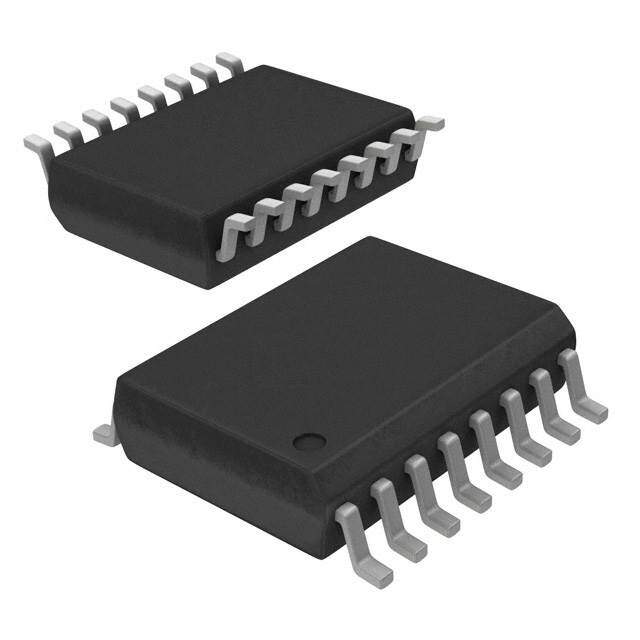
| 封装/外壳 | 16-SOIC(0.295",7.50mm 宽) |
| 封装/箱体 | SOIC-16 |
| 工作温度 | -40°C ~ 150°C |
| 工厂包装数量 | 40 |
| 技术 | 容性耦合 |
| 接收器滞后 | 150mV |
| 数据速率 | 40Mbps |
| 最大工作温度 | + 85 C |
| 最大数据速率 | 40 Mb/s |
| 最小工作温度 | - 40 C |
| 标准包装 | 40 |
| 电压-电源 | 3.15 V ~ 5.5 V, 4.75 V ~ 5.25 V |
| 电压-隔离 | 4000Vpk |
| 电源电压-最大 | 5.5 V |
| 电源电压-最小 | 3.15 V |
| 电源电流 | 11 mA |
| 类型 | RS422, RS485 |
| 系列 | ISO1176 |
| 绝缘电压 | 4 kVrms |
| 脉宽失真(最大) | - |
| 输入-输入侧1/输入侧2 | 2/1 |
| 通道数 | 3 |
| 通道类型 | 单向 |
| 隔离式电源 | 是 |
| 驱动器/接收器数 | 1/1 |

.jpg)


- 商务部:美国ITC正式对集成电路等产品启动337调查
- 曝三星4nm工艺存在良率问题 高通将骁龙8 Gen1或转产台积电
- 太阳诱电将投资9.5亿元在常州建新厂生产MLCC 预计2023年完工
- 英特尔发布欧洲新工厂建设计划 深化IDM 2.0 战略
- 台积电先进制程称霸业界 有大客户加持明年业绩稳了
- 达到5530亿美元!SIA预计今年全球半导体销售额将创下新高
- 英特尔拟将自动驾驶子公司Mobileye上市 估值或超500亿美元
- 三星加码芯片和SET,合并消费电子和移动部门,撤换高东真等 CEO
- 三星电子宣布重大人事变动 还合并消费电子和移动部门
- 海关总署:前11个月进口集成电路产品价值2.52万亿元 增长14.8%

PDF Datasheet 数据手册内容提取
Product Sample & Technical Tools & Support & Folder Buy Documents Software Community ISO1176 SLLS897E–MARCH2008–REVISEDJUNE2015 ISO1176 Isolated RS-485 Profibus Transceiver 1 Features 3 Description • MeetsorExceedstheRequirementsof The ISO1176 device is an isolated differential line 1 transceiver designed for use in PROFIBUS EN50170andTIA/EIA-485-A applications. The device is ideal for long transmission • SignalingRatesupto40Mbps linesbecausethegroundloopisbrokentoprovidefor • DifferentialOutputExceeds2.1V(54-ΩLoad) operation with a much larger common-mode voltage • LowBusCapacitance– 10pF(Maximum) range. The symmetrical isolation barrier of each device is tested to provide 2500 V of isolation per • Upto160TransceiversonaBus RMS UL between the line transceiver and the logic level • 50kV/μsTypicalTransientImmunity interface. • Fail-SafeReceiverforBusOpen,Short,Idle Thegalvanicallyisolateddifferentialbustransceiveris • 3.3-VInputsare5-VTolerant an integrated circuit designed for bidirectional data • Bus-PinESDProtection communication on multipoint bus-transmission lines. The transceiver combines a galvanically isolated – 16-kVHBMBetweenBusPinsandGND2 differential line driver and differential input line – 6-kVHBMBetweenBusPinsandGND1 receiver. The driver has an active-high enable with • SafetyandRegulatoryApprovals isolated enable-state output on the ISODE pin (pin 10)tofacilitatedirectioncontrol.Thedriverdifferential – 4000-V Isolation,560-V V perDINV PK PK IORM outputs and the receiver differential inputs connect VDEV0884-10(VDEV0884-10):2006-12 internally to form a differential input/output (I/O) bus andDINEN61010-1 port that is designed to offer minimum loading to the – 2500VRMSIsolationRatingperUL1577 busallowingupto160nodes. – 4000V IsolationRatingperCSACA5Aand PK The PV pin (pin 7) is provided as a full-chip enable IEC60950-1 option. All device outputs become high impedance when a logic low is applied to the PV pin. For more 2 Applications information, see the function tables in Device FunctionalModes. • Profibus • FactoryAutomation DeviceInformation(1) • NetworkedSensors PARTNUMBER PACKAGE BODYSIZE(NOM) • MotorandMotionControl ISO1176 SOIC(16) 10.30mm×7.50mm • HVAandBuildingAutomationNetworks (1) For all available packages, see the orderable addendum at • NetworkedSecurityStations theendofthedatasheet. SimplifiedSchematic ISO1176 Function Diagram 13 N B R 34 ATIO 12 A RE L O 6 S D C I 7 NI PV A DE 5 ALV 10 ISODE G 1 An IMPORTANT NOTICE at the end of this data sheet addresses availability, warranty, changes, use in safety-critical applications, intellectualpropertymattersandotherimportantdisclaimers.PRODUCTIONDATA.
ISO1176 SLLS897E–MARCH2008–REVISEDJUNE2015 www.ti.com Table of Contents 1 Features.................................................................. 1 9 DetailedDescription............................................ 18 2 Applications........................................................... 1 9.1 Overview.................................................................18 3 Description............................................................. 1 9.2 FunctionalBlockDiagram.......................................18 4 RevisionHistory..................................................... 2 9.3 FeatureDescription.................................................19 9.4 DeviceFunctionalModes........................................21 5 Description(continued)......................................... 4 10 ApplicationandImplementation........................ 24 6 PinConfigurationandFunctions......................... 4 10.1 ApplicationInformation..........................................24 7 Specifications......................................................... 5 10.2 TypicalApplication................................................24 7.1 AbsoluteMaximumRatings......................................5 11 PowerSupplyRecommendations..................... 28 7.2 ESDRatings ............................................................5 12 Layout................................................................... 28 7.3 RecommendedOperatingConditions.......................5 7.4 ThermalInformation..................................................6 12.1 LayoutGuidelines.................................................28 7.5 ElectricalCharacteristics:ISODE-Pin.......................6 12.2 LayoutExample....................................................29 7.6 SupplyCurrent..........................................................6 13 DeviceandDocumentationSupport................. 30 7.7 ElectricalCharacteristics:Driver...............................7 13.1 DocumentationSupport .......................................30 7.8 ElectricalCharacteristics:Receiver..........................8 13.2 CommunityResources..........................................30 7.9 PowerDissipationCharacteristics............................8 13.3 Trademarks...........................................................30 7.10 SwitchingCharacteristics:Driver............................8 13.4 ElectrostaticDischargeCaution............................30 7.11 SwitchingCharacteristics:Receiver........................9 13.5 Glossary................................................................30 7.12 TypicalCharacteristics..........................................10 14 Mechanical,Packaging,andOrderable Information........................................................... 30 8 ParameterMeasurementInformation................12 4 Revision History NOTE:Pagenumbersforpreviousrevisionsmaydifferfrompagenumbersinthecurrentversion. ChangesfromRevisionD(March2010)toRevisionE Page • AddedPinConfigurationandFunctionssection,ESDRatingstable,FeatureDescriptionsection,DeviceFunctional Modes,ApplicationandImplementationsection,PowerSupplyRecommendationssection,Layoutsection,Device andDocumentationSupportsection,andMechanical,Packaging,andOrderableInformationsection .............................. 1 • VDEstandardchangedtoDINVVDEV0884-10(VDEV0884-10):2006-12...................................................................... 1 • ChangedtheIEC60664-1RatingsTable.BasicisolationgroupSPECIFICATIONentryFrom:IIIaTo:II......................... 19 ChangesfromRevisionC(October2008)toRevisionD Page • Added560-VpeakV tothefirstFeaturesList.................................................................................................................. 1 IORM • AddedUL1577,IEC60747-5-2(VDE0884,Rev.2),totheFeaturesList............................................................................ 1 • AddedInputpulsewidthMIN=10nstotheRECOMMENDEDOPERATINGCONDITIONStable..................................... 5 • AddedtheCSAcolumntotheRegulatoryInformationtable................................................................................................ 20 • ChangedtheISO1176“StickyBit”Issuesection................................................................................................................. 26 ChangesfromRevisionB(June2008)toRevisionC Page • ChangedthetextinthesecondparagraphoftheDESCRIPTIONFrom:"wheneverthedriverisdisabledorV = CC2 0"To:"allowingupto160nodes.".......................................................................................................................................... 1 ChangesfromRevisionA(May2008)toRevisionB Page • ChangedL(IO1),Minimumairgap(Clearance)inthePACKAGECHARACTERISTICStableFrom:MIN=7.7mm To:8.34mm........................................................................................................................................................................... 19 2 SubmitDocumentationFeedback Copyright©2008–2015,TexasInstrumentsIncorporated ProductFolderLinks:ISO1176
ISO1176 www.ti.com SLLS897E–MARCH2008–REVISEDJUNE2015 ChangesfromOriginal(March2008)toRevisionA Page • Added3.3-VInputsare5-VToleranttotheFeaturesList...................................................................................................... 1 • AddedtheBus-PinESDProtectionbulletandsubbulletstotheFeaturesList..................................................................... 1 • AddedBuspinstoGND1andBuspinstoGND2totheESDinformationintheHandlingRatingtable............................... 5 • AddedtheAPPLICATIONINFORMATIONsection.............................................................................................................. 24 Copyright©2008–2015,TexasInstrumentsIncorporated SubmitDocumentationFeedback 3 ProductFolderLinks:ISO1176
ISO1176 SLLS897E–MARCH2008–REVISEDJUNE2015 www.ti.com 5 Description (continued) Any cabled I/O can be subjected to electrical noise transients from various sources. These noise transients can causedamagetothetransceiverand/ornearbysensitivecircuitryiftheyareofsufficientmagnitudeandduration. TheISO1176cansignificantlyreducetheriskofdatacorruptionanddamagetoexpensivecontrolcircuits. Thedeviceischaracterizedforoperationovertheambienttemperaturerangeof –40°Cto+85°C. 6 Pin Configuration and Functions DWPackage 16-PinSOIC TopView V V CC1 1 16 CC2 GND1 2 15 GND2 R 3 14 NC RE 4 13 B DE 5 12 A D 6 11 NC PV 7 10 ISODE GND1 8 9 GND2 PinFunctions PIN I/O DESCRIPTION NAME NO. A 12 I/O Noninvertingbusoutput B 13 I/O Invertingbusoutput D 6 I Driverinput DE 5 I Driverlogic-highenable GND1 2,8 — Logic-sideground;internallyconnected GND2 9,15 — Bus-sideground;internallyconnected ISODE 10 — Bus-sidedriverenableoutput NC 11,14 — Notconnectedinternally;maybeleftfloating ISO1176chipenable,logichighappliedimmediatelyafterpowerupfordeviceoperation. PV 7 I Alogiclow3-statesalloutputs. R 3 O Receiveroutput RE 4 I Receiverlogic-lowenable V 1 — Logicsidepowersupply CC1 V 16 — Bussidepowersupply CC2 4 SubmitDocumentationFeedback Copyright©2008–2015,TexasInstrumentsIncorporated ProductFolderLinks:ISO1176
ISO1176 www.ti.com SLLS897E–MARCH2008–REVISEDJUNE2015 7 Specifications 7.1 Absolute Maximum Ratings overoperatingjunctiontemperaturerangeunlessotherwisenoted(1) MIN MAX UNIT V Supplyvoltage(2) V ,V –0.5 7 V CC CC1 CC2 V VoltageatanybusI/Opins –9 14 V O V Voltageinput D,DEorRE –0.5 7 V I I Receiveroutputcurrent –10 10 mA O T Maximumjunctiontemperature 170 °C J T Storagetemperature -65 150 °C stg (1) StressesbeyondthoselistedunderAbsoluteMaximumRatingsmaycausepermanentdamagetothedevice.Thesearestressratings only,andfunctionaloperationofthedeviceattheseoranyotherconditionsbeyondthoseindicatedunderRecommendedOperating Conditionsisnotimplied.Exposuretoabsolute-maximum-ratedconditionsforextendedperiodsmayaffectdevicereliability.Allvoltage valuesarewithrespecttothenetworkgroundterminalunlessotherwisenoted. (2) AllvoltagevaluesexceptdifferentialI/Obusvoltagesarewithrespecttothereferencednetworkgroundterminalandarepeakvoltage values. 7.2 ESD Ratings VALUE UNIT Humanbodymodel(HBM),perANSI/ESDA/JEDECJS- Buspinsto2,8 ±6000 001(1) Buspinsto9,15 ±16000 Electrostatic V Allpins ±4000 V (ESD) discharge Chargeddevicemodel(CDM),perJEDECspecificationJESD22-C101,allpins(2) ±1000 Machinemodel(MM),perANSI/ESDS5.2-1996,allpins ±200 (1) JEDECdocumentJEP155statesthat500-VHBMallowssafemanufacturingwithastandardESDcontrolprocess. (2) JEDECdocumentJEP157statesthat250-VCDMallowssafemanufacturingwithastandardESDcontrolprocess. 7.3 Recommended Operating Conditions MIN NOM MAX UNIT Logic-sidesupplyvoltage,V (withrespecttoGND1) 3.15 5.5 CC1 V V CC Bus-sidesupplyvoltage,V (withrespecttoGND2) 4.75 5.25 CC2 V VoltageateitherbusI/Oterminal A,B –7 12 V CM PV,RE 2 5.5 V High-levelinputvoltage V IH D,DE 0.7V CC1 PV,RE 0 0.8 V Low-levelinputvoltage V IL D,DE 0.3V CC1 V Differentialinputvoltage AwithrespecttoB –12 12 V ID Driver –70 70 I Outputcurrent mA O Receiver –8 8 Inputpulsewidth 10 ns T Ambienttemperature –40 25 85 °C A T Junctiontemperature 150 °C J Copyright©2008–2015,TexasInstrumentsIncorporated SubmitDocumentationFeedback 5 ProductFolderLinks:ISO1176
ISO1176 SLLS897E–MARCH2008–REVISEDJUNE2015 www.ti.com 7.4 Thermal Information ISO1176 THERMALMETRIC(1) DW[SOIC] UNIT 16PINS High-Kboard 81.4 R Junction-to-ambientthermalresistance °C/W θJA Low-Kboard 168 R Junction-to-case(top)thermalresistance 41.4 °C/W θJC(top) R Junction-to-boardthermalresistance 46.4 °C/W θJB ψ Junction-to-topcharacterizationparameter 13.1 °C/W JT ψ Junction-to-boardcharacterizationparameter 45.8 °C/W JB R Junction-to-case(bottom)thermalresistance N/A °C/W θJC(bot) (1) Formoreinformationabouttraditionalandnewthermalmetrics,seetheSemiconductorandICPackageThermalMetricsapplication report,SPRA953. 7.5 Electrical Characteristics: ISODE-Pin overrecommendedoperatingconditions(unlessotherwisenoted) PARAMETER TESTCONDITIONS MIN TYP MAX UNIT I =–8mA V –0.8 4.6 OH CC2 V High-leveloutputvoltage V OH I =–20μA V –0.1 5 OH CC2 I =8mA 0.2 0.4 OL V Low-leveloutputvoltage V OL I =20μA 0 0.1 OL 7.6 Supply Current overrecommendedoperatingconditions(unlessotherwisenoted) PARAMETER TESTCONDITIONS MIN TYP MAX UNIT DEat0V 4 6 3V DEatV ,2Mbps 5 CC1 DEatV ,25Mbps 6 CC1 I Logic-sideRMSsupplycurrent mA CC1 DEat0V 7 10 5.5V DEatV ,2Mbps 8 CC1 DEatV ,25Mbps 11 CC1 DEat0V 15 18 I Bus-sideRMSsupplycurrent 5.25V DEatV ,2Mbps,54-Ωload 70 mA CC2 CC1 DEatV ,25Mbps,54-Ωload 75 CC1 6 SubmitDocumentationFeedback Copyright©2008–2015,TexasInstrumentsIncorporated ProductFolderLinks:ISO1176
ISO1176 www.ti.com SLLS897E–MARCH2008–REVISEDJUNE2015 7.7 Electrical Characteristics: Driver overrecommendedoperatingconditions(unlessotherwisenoted) PARAMETER TESTCONDITIONS MIN TYP MAX UNIT V Open-circuitdifferentialoutputvoltage |V –V |,Figure8 1.5 V V OD A B CC2 SeeFigure9andFigure13 2.1 Steady-statedifferentialoutputvoltage |VOD(SS)| magnitude Common-modeloadingwithVtestfrom–7 2.1 V Vto12V,SeeFigure10 Changeinsteady-statedifferentialoutput |ΔV | R =54Ω,SeeFigure11andFigure12 –0.2 0.2 V OD(SS) voltagebetweenlogicstates L V Steady-statecommon-modeoutputvoltage 2 3 OC(SS) Changeinsteady-statecommon-modeoutput ΔV R =54Ω,SeeFigure11andFigure12 –0.2 0.2 V OC(SS) voltage L V Peak-to-peakcommon-modeoutputvoltage 0.5 OC(PP) Differentialoutputvoltageover-and V SeeFigure13andFigure17 10% V OD(RING) undershoot OD(pp) V Inputvoltagehysteresis SeeFigure14 150 mV I(HYS) D,DEat0VorV –10 10 CC1 I Inputcurrent μA I PV(1)at0VorV 120 CC1 I Outputcurrentwithpoweroff V ≤2.5V Seereceiverinput O(OFF) CC currentinElectrical I High-impedancestateoutputcurrent DEat0V Characteristics: OZ Receiver I Peakshort-circuitoutputcurrent V =–7Vto12V –250 250 OS(P) OS DEatV ,See V =12V,Dat CC OS 135 Figure15and GND1 mA IOS(SS) Steady-stateshort-circuitoutputcurrent Figure16 V =–7V,Dat OS –135 V CC1 SeereceiverC in IN Electrical C Differentialoutputcapacitance OD Characteristics: Receiver CMTI Common-modetransientimmunity SeeFigure27 25 kV/μs (1) ThePVpinhasa50-kΩpullupresistorandleakagecurrentdependsonsupplyvoltage. Copyright©2008–2015,TexasInstrumentsIncorporated SubmitDocumentationFeedback 7 ProductFolderLinks:ISO1176
ISO1176 SLLS897E–MARCH2008–REVISEDJUNE2015 www.ti.com 7.8 Electrical Characteristics: Receiver overrecommendedoperatingconditions(unlessotherwisenoted) PARAMETER TESTCONDITIONS MIN TYP MAX UNIT VIT(+) Positive-goingdifferentialinputvoltagethreshold IO=–8mA –80 –10 mV SeeFigure22 VIT(–) Negative-goingdifferentialinputvoltagethreshold IO=8mA –200 –120 mV Vhys Hysteresisvoltage(VIT+–VIT-) 40 mV VOH High-leveloutputvoltage VCC1at3.3VandVCC2at VSIeDe=F2ig0u0rem2V2, IIOOHH==––820mAμA VVCCCC11––00..41 3.33 V VOL Low-leveloutputvoltage 5V VSIeDe=F–ig2u0r0em22V, IIOOLL==280mμAA 0.02 00..41 V VOH High-leveloutputvoltage VCC1at5VandVCC2at5 VSIeDe=F2ig0u0rem2V2, IIOOHH==––820mAμA VVCCCC11––00..81 4.56 V VOL Low-leveloutputvoltage V VSIeDe=F–ig2u0r0em22V, IIOOLL==–820mμAA 0.02 00..41 V IA,IB VCC=4.75Vor5.25V IIAB((OOFFFF)) Buspininputcurrent VOIth=e–r7inVpuotr=120VV, VCC2=0V –160 200 μA II Receiverenableinputcurrent RE=0V –50 50 μA IOZ High-impedancestateoutputcurrent RE=VCC1 –1 1 μA RID Differentialinputresistance A,B 48 kΩ Testinputsignalisa1.5-MHzsinewavewith CID Differentialinputcapacitance 1Vppamplitude,CDismeasuredacross 7 10 pF AandB CMR Common-moderejection SeeFigure26 4 V 7.9 Power Dissipation Characteristics PARAMETER VALUE UNIT V =V =5.25V,T =150°C,CL=15pF, P PowerDissipation CC1 CC2 J 220 mW D Inputa20MHz50%duty-cyclesquarewave 7.10 Switching Characteristics: Driver overrecommendedoperatingconditions(unlessotherwisenoted) PARAMETER TESTCONDITIONS MIN TYP MAX UNIT tpLH,tpHL Propagationdelaytime VCC1at5V 35 ns tsk(p) Pulseskew(|tpHL–tpLH|) VCC2at5V 2 5 ns tpLH,tpHL Propagationdelaytime VCC1at3.3V SeeFigure17 40 ns tsk(p) Pulseskew(|tpHL–tpLH|) VCC2at5V 2 5 ns t Differentialoutputsignalrisetime 2 3 7.5 ns r t Differentialoutputsignalfalltime 2 3 7.5 ns f t DEtoISODEpropdelay SeeFigure21 30 ns pDE t ,t Outputtransitionskew SeeFigure18 1 ns t(MLH) t(MHL) t ,t p(AZH) p(BZH) Propagationdelaytime,high-impedance-to-activeoutput 80 ns t ,t p(AZL) p(BZL) C =50pF, L tp(AHZ),tp(BHZ) Propagationdelaytime,active-to-high-impedanceoutput REat0V, 80 ns tp(ALZ),tp(BLZ) SeeFigure19and Figure20 |t –t | p(AZL) p(BZH) Enableskewtime 0.55 1.5 ns |t –t | p(AZH) p(BZL) t Timefromapplicationofshort-circuittocurrentfoldback SeeFigure16 0.5 μs (CFB) t Timefromapplicationofshort-circuittothermalshutdown T =25°C,SeeFigure16 100 μs (TSD) A 8 SubmitDocumentationFeedback Copyright©2008–2015,TexasInstrumentsIncorporated ProductFolderLinks:ISO1176
ISO1176 www.ti.com SLLS897E–MARCH2008–REVISEDJUNE2015 7.11 Switching Characteristics: Receiver overrecommendedoperatingconditions(unlessotherwisenoted) PARAMETER TESTCONDITIONS MIN TYP MAX UNIT t ,t Propagationdelaytime 50 ns pLH pHL V at5V,V at5V CC1 CC2 t Pulseskew(|t –t |) 2 5 ns sk(p) pHL pLH t ,t Propagationdelaytime 55 ns pLH pHL V at3.3V,V at5V SeeFigure23 CC1 CC2 t Pulseskew(|t –t |) 2 5 ns sk(p) pHL pLH t Outputsignalrisetime 2 4 ns r t Outputsignalfalltime 2 4 ns f tpZH Propagationdelaytime,high-impedance-to-high-leveloutput DEatVCC1, 13 25 ns t Propagationdelaytime,high-level-to-high-impedanceoutput SeeFigure24 13 25 ns pHZ tpZL Propagationdelaytime,high-impedance-to-low-leveloutput DEatVCC, 13 25 ns t Propagationdelaytime,low-level-to-high-impedanceoutput SeeFigure25 13 25 ns pLZ Copyright©2008–2015,TexasInstrumentsIncorporated SubmitDocumentationFeedback 9 ProductFolderLinks:ISO1176
ISO1176 SLLS897E–MARCH2008–REVISEDJUNE2015 www.ti.com 7.12 Typical Characteristics 5 100 No Load −V 4.54 VCC= 5V VCC= 5.25 V 100Ω 8900 TA= 25°C ICC2 e oltagput V 3.53 VCC= 4.75 V 50Ω ent - mA 6700 Out 2.5 urr 50 ntial 2 ply C 40 e p Differ 1.5 - SuC 30 5 V VCC1 −OD 1 IC 20 ICC1 3.3 V VCC1 V 0.5 10 TA= 25C 0 0 0 20 40 60 80 0 5 10 15 20 IL−Load Current−mA Signalling Rate - Mbps Figure1.DifferentialOutputVoltagevsLoadCurrent Figure2.RMSSupplyCurrentvsSignalingRate 0.35 4 RL= 54Ω, RL= 54Ω, CL= 50 pF CL= 50 pF s 0.3 3.75 n w− VCC= 4.75 V s 3.5 VCC= 4.75 V e 0.25 n ansition Sk 0.2 VCC= 5 V ime−Fall T 3.235 VCC= 5 V rer Output T 00.1.15 VCC= 5.25 V Driver Rise, 22.7.55 VCC= 5.25 V v Dri 0.05 2.25 0 2 −40 −15 10 35 60 85 −40 −15 10 35 60 85 TA−Free-Air Temperature−°C TA−Free-Air Temperature−°C Figure3.DriverOutputTransitionSkewvsFree-Air Figure4.DriverRiseandFallTimevsFree-AirTemperature Temperature 0.7 -99 15 pF Load 0.6 VCC= 4.75 V -89 TA= 25°C -79 −ns 0.5 mA -69 e Skew 0.4 VCC= 5.25 V urrent - -59 bl VCC= 5 V C -49 na 0.3 ut Driver E 0.2 - OutpO --3299 I -19 0.1 RL= 110Ω, -9 CL= 50 pF 0 1 −40 −15 10 35 60 85 0 1 2 3 4 5 TA−Free-Air Temperature−°C V - Output Voltage - V O Figure5.DriverEnableSkewvsFree-AirTemperature Figure6.High-LevelOutputVoltagevsHigh-LevelOutput Current 10 SubmitDocumentationFeedback Copyright©2008–2015,TexasInstrumentsIncorporated ProductFolderLinks:ISO1176
ISO1176 www.ti.com SLLS897E–MARCH2008–REVISEDJUNE2015 Typical Characteristics (continued) 110 15 pF Load 100 T = 25°C A 90 A 80 m nt - 70 e urr 60 C put 50 ut O 40 - O I 30 20 10 0 0 1 2 3 4 5 V - Output Voltage - V O Figure7.Low-LevelOutputVoltagevsLow-LevelOutputCurrent Copyright©2008–2015,TexasInstrumentsIncorporated SubmitDocumentationFeedback 11 ProductFolderLinks:ISO1176
ISO1176 SLLS897E–MARCH2008–REVISEDJUNE2015 www.ti.com 8 Parameter Measurement Information V CC1 DE IOA A 0 or I VCC1 D VOD B GND 1 GND 2 IOB VI VOB VOA GND 1 GND 2 Figure8. OpenCircuitVoltageTestCircuit V CC1 DE IOA A 0 or I VCC1 ID VOD 54W B GND 1 GND 2 IOB VI VOB VOA GND 1 GND 2 Figure9. V TestCircuit OD V CC2 DE 375W A D + 0 or 3 V B VOD 60W - -7 V to 12 V GND 2 375W Figure10. DriverV WithCommon-ModeLoadingTestCircuit OD 12 SubmitDocumentationFeedback Copyright©2008–2015,TexasInstrumentsIncorporated ProductFolderLinks:ISO1176
ISO1176 www.ti.com SLLS897E–MARCH2008–REVISEDJUNE2015 Parameter Measurement Information (continued) V CC1 DE IOA RL 2 A 0 or II VCC1 D B VOD RL GND 1 GND 2 IOB 2 VI VOB VOA VOC GND 1 GND 2 Figure11. DriverV andV WithoutCommon-ModeLoadingTestCircuit OD OC V CC1 DE IOA R2L A VA A I Input I D VOD B VB B Generator PRR = 500 kHz, RL V 5tt0<% 6 d nusty, ZcOyc=le 5, 0trΩ< 6 ns, VIGND 1 GND 2 IOB 2 OC VOC(p-p) VOB VOA VOC VOC(SS) GND 1 GND 2 Figure12. Steady-StateOutputVoltageTestCircuitandVoltageWaveforms V DO(RING) V V DO(SS) OD(pp) 0 V Differential Figure13. V WaveformandDefinitions OD(RING) Copyright©2008–2015,TexasInstrumentsIncorporated SubmitDocumentationFeedback 13 ProductFolderLinks:ISO1176
ISO1176 SLLS897E–MARCH2008–REVISEDJUNE2015 www.ti.com Parameter Measurement Information (continued) V CC1 DE IOA A I V0C oCr1 I D B VOD 54W GND 1 GND 2 IOB VI VOB VOA GND 1 GND 2 Figure14. InputVoltageHysteresisTestCircuit DE 250 IOS A A m D 0.5W nt - e B IOS Curr 120 Vos put 60 ut GND 1 GND 2 O GND 2 t(CFB) time t (TSD) Figure15. DriverShort-CircuitTestCircuitandWaveforms(Short-CircuitAppliedatTimet=0) DE 250 IOS A A m D nt - e B IOS urr 120 C Vos ut 60 p GND 1 GND 2 ut O GND 2 t(CFB) time t (TSD) Figure16. I SteadyStateShort-CircuitOutputCurrentTestCircuit OS(SS) DE 3 V V CC1 A D R = 54WVOD CL= 50 pF VI 1.5 V 1.5 V L ± 20% GeInnepruattor VI 50W B ±1% tPLH tPHL VOD (H) 90% 90% GND 1 CLIncludes Fixture and 0 V 0 V Generator PRR = 500 kHz, 50 % Duty Instrumentation Capacitance VOD 10% 10% Cycle, t <6 ns, Z = 50W V r O tr tf OD (L) Figure17. DriverSwitchingTestCircuitandWaveforms 14 SubmitDocumentationFeedback Copyright©2008–2015,TexasInstrumentsIncorporated ProductFolderLinks:ISO1176
ISO1176 www.ti.com SLLS897E–MARCH2008–REVISEDJUNE2015 Parameter Measurement Information (continued) DE V CC1 A 50 % 50 % D A GeInnepruattor VI 50W B R±1L%= 54W C±2L0=% 50 pF VO B tt(MHL) tt(MLH) GND 1 GND 2 VOA VOB 50 % 50 % Generator PRR = 500 kHz, 50% Duty Cycle, t <6 ns, t <6 ns, Z = 50W r f O C Includes Fixture and L Instrumentation Capacitance Figure18. DriverOutputTransitionSkewTestCircuitandWaveforms R = 110W L V A CC2 DE 1.5 V C = 50 pF L V = 0 V D t(AZL) t(ALZ) IN B R = 110W A 50% VOL+0.5 V DE L 0 V t(BZH) t(BHZ) Signal Generator 50W VOAVOB C = 50 pF B 50% VO-0.5 V L GND1 GND2 Generator PRR = 500 kHz, 50% Duty Cycle, t <6 ns, t <6 ns, Z = 50W r f O Figure19. DriverEnableandDisableTest,DatLogicLowTestCircuitandWaveforms R = 110W L 0 V A C = 50 pF 1.5 V L DE D VIN= 3 V t(AZH) t(AHZ) DE B RL= 110W A 50% VOH-0.5 V V CC2 GeSnigenraatlor 50W VOAVOB C = 50 pF B t(BZL) t(BLZ) L 50% V +0.5 V OL GND 1 GND 2 Generator PRR = 500 kHz, 50% Duty Cycle, t <6 ns, t <6 ns, Z = 50W r f O Figure20. DriverEnableandDisableTest,DatLogicHighTestCircuitandWaveforms Copyright©2008–2015,TexasInstrumentsIncorporated SubmitDocumentationFeedback 15 ProductFolderLinks:ISO1176
ISO1176 SLLS897E–MARCH2008–REVISEDJUNE2015 www.ti.com Parameter Measurement Information (continued) V V CC1 CC2 DE 50% 50% D ISODE V = V IN CC1 tPDE_LH tPDE_HL C = 15 pF DE L ± 20% 50% 50% GeSnigenraatlor 50W ISODE GND 1 GND 2 Generator PRR = 500 kHz, 50% Duty Cycle, t <6 ns, t <6 ns, Z = 50W r f O Figure21. DEtoISODEPropDelayTestCircuitandWaveforms I O V ID V O Figure22. ReceiverDCParameterDefinitions Signal Generator 50W Input B 1.5 V A 50% PRR = 100 kHz, 50% Duty Cycle, R IO InputA t <6 ns, t <6 ns, Z = 50W VID 0 V r f O B VO tpLH tpHL CL= 15 pF 90% VOH Signal 50W (Includes Probe and 1.5 V Generator Jig Capacitance) Output 10% VOL tr tf Figure23. ReceiverSwitchingTestCircuitandWaveforms V D CC V DE CC A 3 V RE 54W 1.5 V 1.5 V B 0 V 1 kW tpZH tpHZ R 0 V VO V -0.5 V OH CL= 15 pF 1.5 V RE (Includes Probe and R Jig Capacitance) GND Signal 50W Generator PRR = 100 kHz, 50% duty cycle, t <6 ns, t <6 ns, Z = 50W r f O Figure24. ReceiverEnableTestCircuitandWaveforms,DataOutputHigh 16 SubmitDocumentationFeedback Copyright©2008–2015,TexasInstrumentsIncorporated ProductFolderLinks:ISO1176
ISO1176 www.ti.com SLLS897E–MARCH2008–REVISEDJUNE2015 Parameter Measurement Information (continued) D 0 V DE V CC A RE 3 V 54W 1.5 V 1.5 V B 0 V 1 kW tpZL tpLZ R VCC1 R VOH CL= 15 pF 1.5 V V +0.5 V (Includes Probe and OL RE Jig Capacitance) VOL Signal 50W Generator PRR = 100 kHz, 50% duty cycle, t <6 ns, t <6 ns, Z = 50W r f O Figure25. ReceiverEnableTestCircuitandWaveforms,DataOutputLow A VINPUT 100 nF 470 nF f = 1 to 50 MHz 50W R Ampl. = ± 5 V B RE 50W DE 2.2 kW VR Scope 2.2 kW D V OFFSET = -2 V to 7 V Scope GND V CC 100 nF Figure26. Common-ModeRejectionTestCircuit 2 V C = 0.1mF VCC1 VCC2 ±1% A C = 0.1mF ± 1% DE GND1 D S1 54W VOHor VOL B 0.8 V Success / Fail Criterion: R Stable V or V Outputs OH OL RE V or V 1 kW OH OL GND1 GND2 C = 15 pF L (Includes Probe and Jig Capacitance) VTEST Figure27. Common-ModeTransientImmunityTestCircuit Copyright©2008–2015,TexasInstrumentsIncorporated SubmitDocumentationFeedback 17 ProductFolderLinks:ISO1176
ISO1176 SLLS897E–MARCH2008–REVISEDJUNE2015 www.ti.com 9 Detailed Description 9.1 Overview The ISO1176 is an isolated half-duplex differential line transceiver that meets the requirements of EN 50170 and TIA/EIA 485/422 applications. The device is rated to provide galvanic isolation of up to 2500 V for 60 s per RMS UL 1577. The device has active-high driver enable and active-low receiver enable functions to control the data flow.Thedevicehasmaximumdatatransmissionspeedof40Mbps. When the driver enable pin, DE, is logic high, the differential outputs A and B follow the logic states at data input D. A logic high at D causes A to turn high and B to turn low. In this case, the differential output voltage defined as V = V – V is positive. When D is low, the output states reverse, B turns high, A becomes low, and V OD (A) (B) OD isnegative.WhenDEislow,bothoutputsturnhigh-impedance.Inthiscondition,thelogicstateatDisirrelevant. The DE pin has an internal pulldown resistor to ground, thus when left open the driver is disabled (high- impedance) by default. The D pin has an internal pullup resistor to V , thus, when left open while the driver is CC enabled,outputAturnshighandBturnslow. When the receiver enable pin, RE, is logic low, the receiver is enabled. When the differential input voltage defined as V = V – V is positive and higher than the positive input threshold, V , the receiver output, R, ID (A) (B) IT+ turns high. When V is negative and less than the negative and lower than the negative input threshold, V , ID IT– the receiver output, R, turns low. If V is between V and V the output is indeterminate. When RE is logic ID IT+ IT– high or left open, the receiver output is high-impedance and the magnitude and polarity of V are irrelevant. ID Internal biasing of the receiver inputs causes the output to go failsafe-high when the transceiver is disconnected fromthebus(open-circuit),thebuslinesareshorted(short-circuit),orthebusisnotactivelydriven(idlebus). 9.2 Functional Block Diagram V V CC1 CC2 B R A RE N O TI A L O D S I C NI A PV V L A G ISODE DE GND1 GND2 18 SubmitDocumentationFeedback Copyright©2008–2015,TexasInstrumentsIncorporated ProductFolderLinks:ISO1176
ISO1176 www.ti.com SLLS897E–MARCH2008–REVISEDJUNE2015 9.3 Feature Description 9.3.1 InsulationandSafety-RelatedPackageCharacteristics overoperatingfree-airtemperaturerange(unlessotherwisenoted) PARAMETER TESTCONDITIONS MIN TYP MAX UNIT L(I01) Minimumairgap(Clearance) Shortestterminal-to-terminaldistance 8.34 mm throughair L(I02) Minimumexternaltracking(Creepage)(1) Shortestterminal-to-terminaldistance 8.1 mm acrossthepackagesurface CTI Trackingresistance(ComparativeTracking DINIEC60112/VDE0303Part1 ≥400 V Index) Minimuminternalgap(InternalClearance) Distancethroughtheinsulation 0.008 mm Inputtooutput,V =500V,TA=25°C,all IO R Isolationresistance pinsoneachsideofthebarriertied >1012 Ω IO togethercreatinga2-terminaldevice C BarriercapacitanceInputtooutput V =0.4sin(4E6πt) 2 pF IO I C Inputcapacitancetoground V =0.4sin(4E6πt) 2 pF I I (1) Creepageandclearancerequirementsshouldbeappliedaccordingtothespecificequipmentisolationstandardsofanapplication.Care mustbetakentomaintainthecreepageandclearancedistanceofaboarddesigntoensurethatthemountingpadsoftheisolatoron theprinted-circuit-board(PCB)donotreducethisdistance. CreepageandclearanceonaPCBbecomeequalaccordingtothemeasurementtechniquesshownintheIsolationGlossary. Techniquessuchasinsertinggroovesand/orribsonaPCBareusedtohelpincreasethesespecifications. 9.3.2 DINVVDEV0884-10InsulationCharacteristics overrecommendedoperatingconditions(unlessotherwisenoted) PARAMETER TESTCONDITIONS SPECIFICATION UNIT V Transientovervoltage t=60s 4000 V IOTM PK V Maximumworkinginsulationvoltage 560 V IORM PK Methodb1,V =V ×1.875,100%Production V Inputtooutputtestvoltage PR IORM 1050 V PR testwitht=1s,Partialdischarge<5pC PK R Insulationresistance V =500VatT >109 Ω S IO S Pollutiondegree 2 9.3.3 IEC60664-1RatingsTable PARAMETER TESTCONDITIONS SPECIFICATION Basicisolationgroup Materialgroup II Ratedmainsvoltage<150V I-IV RMS Installationclassification Ratedmainsvoltage<300V I-III RMS 9.3.4 SafetyLimitingValues Safety limiting intends to prevent potential damage to the isolation barrier upon failure of input or output circuitry. A failure of the I/O can allow low resistance to ground or the supply and, without current-limiting, dissipate sufficient power to overheat the die and damage the isolation barrier potentially leading to secondary system failures. PARAMETER TESTCONDITIONS MIN TYP MAX UNIT R =168°C/W,V =5.5V,T =170°C, I Safetyinput,output,orsupplycurrent DW-16 θJA I J 157 mA S T =25°C A T Maximumcasetemperature DW-16 150 °C S Copyright©2008–2015,TexasInstrumentsIncorporated SubmitDocumentationFeedback 19 ProductFolderLinks:ISO1176
ISO1176 SLLS897E–MARCH2008–REVISEDJUNE2015 www.ti.com The safety-limiting constraint is the absolute maximum junction temperature specified in Absolute Maximum Ratings. The power dissipation and junction-to-air thermal impedance of the device installed in the application hardware determines the junction temperature. The assumed junction-to-air thermal resistance in Thermal Information is that of a device installed in the JESD51-3, Low Effective Thermal Conductivity Test Board for LeadedSurfaceMountPackagesandisconservative. The power is the recommended maximum input voltage times the current. The junction temperature is then the ambienttemperatureplusthepowertimesthejunction-to-airthermalresistance.. 200 VCC1= VCC2= 5.5 V A) m 150 ( nt e urr C g 100 n miti Li y et 50 af S 0 0 50 100 150 200 CaseTemperature (°C) D001 Figure28. DW-16R ThermalDeratingCurveperVDE θJC 9.3.5 RegulatoryInformation VDE CSA UL CertifiedaccordingtoDINVVDEV0884-10 ApprovedunderCSAComponent RecognizedunderUL1577Component (VDEV0884-10):2006-12 AcceptanceNotice5AandIEC60950-1 RecognitionProgram(1) Basicinsulation, 4000V Isolationrating, PK 4000VPKMaximumtransientovervoltage, 560VPKBasicworkingvoltageperCSA SingleProtection,2500VRMS 560V Maximumworkingvoltage 60950-1-07andIEC60950-1(2ndEd) PK Certificatenumber:40016131 Mastercontractnumber:220991 Filenumber:E181974 (1) Productiontested≥3000Vrmsfor1secondinaccordancewithUL1577. 20 SubmitDocumentationFeedback Copyright©2008–2015,TexasInstrumentsIncorporated ProductFolderLinks:ISO1176
ISO1176 www.ti.com SLLS897E–MARCH2008–REVISEDJUNE2015 9.4 Device Functional Modes Table1.DriverFunctionTable(1) V V POWER INPUT ENABLE ENABLEOUTPUT OUTPUTS CC1 CC2 VALID (D) INPUT (ISODE) A B (PV) (DE) (ISO1176) PU PU Horopen H H H H L PU PU Horopen L H H L H PU PU Horopen X L L Z Z PU PU Horopen X open L Z Z PU PU Horopen open H H H L PD PU X X X L Z Z PU PD X X X L Z Z PD PD X X X L Z Z X X L X X L Z Z (1) PU=poweredup,PD=powereddown,H=highlevel,L=lowlevel,X=don’tcare,Z=highimpedance(off) Table2.ReceiverFunctionTable(1) V V POWERVALID DIFFERENTIALINPUT ENABLE OUTPUT CC1 CC2 (PV)(ISO1176) V =(V –V ) (RE) (R) ID A B PU PU Horopen –0.01V≤V L H ID PU PU Horopen –0.2V<V <–0.01V L ? ID PU PU Horopen V ≤–0.2V L L ID PU PU Horopen X H Z PU PU Horopen X open Z PU PU Horopen Open-circuit L H PU PU Horopen Short-circuit L H PU PU Horopen Idle(terminated)bus L H PD PU X X X Z PU PD Horopen X L H PD PD X X X Z X X L X X Z (1) PU=poweredup,PD=powereddown,H=highlevel,L=lowlevel,X=don’tcare,Z=highimpedance(off),?=indeterminate Copyright©2008–2015,TexasInstrumentsIncorporated SubmitDocumentationFeedback 21 ProductFolderLinks:ISO1176
ISO1176 SLLS897E–MARCH2008–REVISEDJUNE2015 www.ti.com D, RE Input DE Input VCC1 VCC1 VCC1 VCC1 VCC1 1 MW 500W 500W 1 MW PV Input ISODE Output V CC2 V V V CC1 CC1 CC1 50 kW 5.5W 500W 11W 3.3 V R Output 5 V R Output V V CC1 CC1 4W 5.5W 6.4W 11W Figure29. EquivalentI/OSchematics 22 SubmitDocumentationFeedback Copyright©2008–2015,TexasInstrumentsIncorporated ProductFolderLinks:ISO1176
ISO1176 www.ti.com SLLS897E–MARCH2008–REVISEDJUNE2015 AInput B Input V V CC2 CC2 16 V 18 kW 16 V 18 kW 90 kW 90 kW Input Input 16 V 18 kW 16 V18 kW Aand B Outputs V CC2 16 V Output 16 V Figure30. EquivalentI/OSchematicsforAandBInputsandOutputs Copyright©2008–2015,TexasInstrumentsIncorporated SubmitDocumentationFeedback 23 ProductFolderLinks:ISO1176
ISO1176 SLLS897E–MARCH2008–REVISEDJUNE2015 www.ti.com 10 Application and Implementation NOTE Information in the following applications sections is not part of the TI component specification, and TI does not warrant its accuracy or completeness. TI’s customers are responsible for determining suitability of components for their purposes. Customers should validateandtesttheirdesignimplementationtoconfirmsystemfunctionality. 10.1 Application Information TheISO1176deviceconsistsofaRS-485transceiver,commonlyusedforasynchronousdatatransmissions.For half-duplex transmission, only one pair is shared for both transmission and reception of data. To eliminate line reflections, each cable end is terminated with a termination resistor, R(T), whose value matches the characteristic impedance, Z0, of the cable. This method, known as parallel termination, allows for higher data ratesoverlongercablelength. 10.2 Typical Application R R R R R R RE A RE A RE A DE B DE B DE B D D D D D D a) Independent driver and b) Combined enable signals for c) Receiver always on receiver enable signals use as directional control pin Figure31. Half-DuplexTransceiverConfigurations 10.2.1 DesignRequirements RS-485 is a robust electrical standard suitable for long-distance networking that may be used in a wide range of applicationswithvaryingrequirements,suchasdistance,datarate,andnumberofnodes. Table3.DesignParameters PARAMETER VALUE PullupandPulldownResistors 1kΩto10kΩ DecouplingCapacitors 100nF 10.2.2 DetailedDesignProcedure Isolating of a circuit insulates it from other circuits and earth, so that noise voltage develops across the insulation rather than circuit components. The most common noise threat to data-line circuits is voltage surges or electrical fast transients that occur after installation. The transient ratings of the ISO1176 standard are sufficient for all but the most severe installations. However, some equipment manufacturers use ESD generators to test equipment transient susceptibility. This practice can exceed insulation ratings. ESD generators simulate static discharges thatmayoccurduringdeviceorequipmenthandlingwithlow-energybuthigh-voltagetransients. 24 SubmitDocumentationFeedback Copyright©2008–2015,TexasInstrumentsIncorporated ProductFolderLinks:ISO1176
ISO1176 www.ti.com SLLS897E–MARCH2008–REVISEDJUNE2015 Aor B C R 16V IN IN VN Bus Return(GND2) C R ISO ISO System Ground(GND1) Figure32. DeviceModelforStaticDischargeTesting Figure 32 models the ISO1176 bus IO connected to a noise generator. C and R is the device, and any other IN IN stray or added capacitance or resistance across the A or B pin to GND2. C and R is the capacitance and ISO ISO resistance between GND1 and GND2 of the ISO1176, plus those of any other insulation (transformer, and so forth).Strayinductanceisassumedtobenegligible. 10.2.2.1 TransientVoltages Fromthismodel,thevoltageattheisolatedbusreturnis Z v = v ISO GND2 N Z +Z ISO IN (1) andisalwayslessthan16VfromV .IftheISO1176istestedasastand-alonedevice, N • R =6x10⁴Ω, IN • C =16x10–12F, IN • R =109Ωand ISO • C =10–12F. ISO Notice from Figure 32 that the resistor ratio determines the voltage ratio at low frequencies, and that the inverse capacitance ratio determines the voltage ration at high frequencies. In the stand-alone case and for low frequencies, v R 109 GND2 = ISO = v R +R 109 +6x10⁴ N ISO IN (2) oressentiallyallofthenoiseappearsacrossthebarrier. Athighfrequencies, 1 v C 1 1 GND2 = ISO = = =0.94 vN 1CISO + 1CIN 1+CISOCIN 1+ 116 (3) and 94% of V appears across the barrier. As long as R is greater than R and C is less than C , most of N ISO IN ISO IN thetransientnoiseappearsacrosstheisolationbarrier,asitshould. Using ESD generators to test equipment transient susceptibility, or considering product claims of ESD ratings greater than the barrier transient ratings of an isolated interface is not recommended. ESD is best managed throughrecessingorcoveringconnectorpinsinaconductiveconnectorshell,andbyproperinstallertraining. Copyright©2008–2015,TexasInstrumentsIncorporated SubmitDocumentationFeedback 25 ProductFolderLinks:ISO1176
ISO1176 SLLS897E–MARCH2008–REVISEDJUNE2015 www.ti.com 10.2.2.2 ISO1176“StickyBit”Issue(UnderCertainConditions) Summary: In applications with sufficient differential noise on the bus, the output of the ISO1176 receiver may “stick”atanincorrectstateforupto30 µs. Description: The ISO1176 isolated Profibus (RS-485) transceiver is rated for signaling up to 40 Mbps on twisted- pair bus lines. The receiver thresholds comply with RS-485 and Profibus specifications; an input differential voltage V = V – V > 200 mV causes a logic High on the R output, and V < –200 mV causes a logic Low on ID A B ID theRoutput.Toassureaknownreceiveroutputwhenthebusisshortedoridle,theupperthresholdissetbelow zero, such that V = 0 mV causes a logic High on the R output. The data sheet specifies a typical upper ID threshold(V )of–80mVandatypicallowerthreshold(V )of–120mV. IT+ IT- At a signaling rate of 40 Mbps, each valid data bit has a duration of 25 ns. At typical Profibus signaling rates of 12 Mbps or lower, each valid data bit has a duration of 83 ns or more. The ISO1176 correctly sets the R output foreachofthesevaliddatabits. In applications with a high degree of differential noise on the bus lines, it is possible to get short periods when an invalid bus voltage triggers a change in state of the internal receiver circuits. An issue with the digital isolation channel in the ISO1176 may cause the invalid receiver state to “stick” rather than immediately transition back to thecorrectstate.Thereceiveroutputwillalwaystransitiontothecorrectstate,butmaystickintheincorrectstate forupto30µs.Thiscancauseatemporarylossofdata. Figure33showstwocaseswhichcouldresultintemporarylossofdata. Case 1 ACTIVE DRIVER STATE RECEIVER POSITIVE THRESHOLD BUS DIFFERENTIALVOLTAGE RECEIVER NEGATIVE THRESHOLD EFFECTIVE PULSE WIDTH REFRESH TIME ISO1176 RECEIVER OUTPUT Case 2 ACTIVE DRIVER STATE DISABLED RECEIVER POSITIVE THRESHOLD BUS DIFFERENTIALVOLTAGE RECEIVER NEGATIVE THRESHOLD EFFECTIVE PULSE WIDTH ISO1176 RECEIVER OUTPUT REFRESH TIME Figure33. "StickyBit"IssueWaveforms 26 SubmitDocumentationFeedback Copyright©2008–2015,TexasInstrumentsIncorporated ProductFolderLinks:ISO1176
ISO1176 www.ti.com SLLS897E–MARCH2008–REVISEDJUNE2015 10.2.3 ApplicationCurve Atmaximumworkingvoltage,ISO1176isolationbarrierhasmorethan28yearsoflife. 100 S R A E Y -- E V at 560 V F IORM PK LI 28 G N KI R O W 10 0 120 250 500 750 880 1000 WORKING VOLTAGE (V ) -- V IORM PK Figure34. Time-DependentDielectricBreakdownTestResults Copyright©2008–2015,TexasInstrumentsIncorporated SubmitDocumentationFeedback 27 ProductFolderLinks:ISO1176
ISO1176 SLLS897E–MARCH2008–REVISEDJUNE2015 www.ti.com 11 Power Supply Recommendations To ensure reliable operation at all data rates and supply voltages, TI recommends a 0.1-μF bypass capacitor at input and output supply pins (V and V ). The capacitors should be placed as close to the supply pins as CC1 CC2 possible. If only a single primary-side power supply is available in an application, isolated power can be generated for the secondary-side with the help of a transformer driver such as TI's SN6501. For such applications, detailed power supply design and transformer selection recommendations are available in SN6501 datasheet(SLLSEA0). 12 Layout 12.1 Layout Guidelines ON-chip IEC-ESD protection is good for laboratory and portable equipment but never sufficient for EFT and surgetransientsoccurringinindustrialenvironments.Therefore,robustandreliablebusnodedesignrequiresthe use of external transient protection devices. Because ESD and EFT transients have a wide frequency bandwidth from approximately 3-MHz to 3-GHz, high-frequency layout techniques must be applied during PCB design. A minimumoffourlayersisrequiredtoaccomplishalowEMIPCBdesign(seeFigure35). • Layer stacking should be in the following order (top-to-bottom): high-speed signal layer, ground plane, power plane,andlow-frequencysignallayer. • Placing a solid ground plane next to the high-speed signal layer establishes controlled impedance for transmissionlineinterconnectsandprovidesanexcellentlow-inductancepathforthereturncurrentflow. • Placing the power plane next to the ground plane creates additional high-frequency bypass capacitance of approximately100pF/in2. • Routing the slower speed control signals on the bottom layer allows for greater flexibility as these signal links usuallyhavemargintotoleratediscontinuitiessuchasvias. • Place the protection circuitry close to the bus connector to prevent noise transients from penetrating your board. • Use V and ground planes to provide low-inductance. High-frequency currents might follow the path of least CC inductanceandnotnecessarilythepathofleastresistance. • Design the protection components into the direction of the signal path. Do not force the transient currents to divertfromthesignalpathtoreachtheprotectiondevice. • Apply 0.1-µF bypass capacitors as close as possible to the V -pins of transceiver, UART, and controller ICs CC ontheboard. • Use at least two vias for V and ground connections of bypass capacitors and protection devices to CC minimizeeffectivevia-inductance. • Use 1-kΩ to 10-kΩ pullup and pulldown resistors for enable lines to limit noise currents in theses lines during transientevents. • Insert pulse-proof resistors into the A and B bus lines if the TVS clamping voltage is higher than the specified maximum voltage of the transceiver bus pins. These resistors limit the residual clamping current into the transceiverandpreventitfromlatchingup. • While pure TVS protection is sufficient for surge transients up to 1 kV, higher transients require metal-oxide varistors (MOVs) which reduce the transients to a few hundred volts of clamping voltage, and transient blockingunits(TBUs)thatlimittransientcurrenttolessthan1mA. • Routing the high-speed traces on the top layer avoids the use of vias (and the introduction of their inductances) and allows for clean interconnects between the isolator and the transmitter and receiver circuits ofthedatalink. If an additional supply voltage plane or signal layer is needed, add a second power and ground plane system to thestacktokeepitsymmetrical.Thismakesthestackmechanicallystableandpreventsitfromwarping.Alsothe powerandgroundplaneofeachpowersystemcanbeplacedclosertogether,thusincreasingthehigh-frequency bypasscapacitancesignificantly. NOTE For detailed layout recommendations, see Application Note Digital Isolator Design Guide, SLLA284. 28 SubmitDocumentationFeedback Copyright©2008–2015,TexasInstrumentsIncorporated ProductFolderLinks:ISO1176
ISO1176 www.ti.com SLLS897E–MARCH2008–REVISEDJUNE2015 12.2 Layout Example High-speedtraces 10mils Groundplane Keepthis spacefree FR-4 40mils fromplanes, 0r~4.5 traces,pads, andvias Powerplane 10mils Low-speedtraces Figure35. RecommendedLayerStack Copyright©2008–2015,TexasInstrumentsIncorporated SubmitDocumentationFeedback 29 ProductFolderLinks:ISO1176
ISO1176 SLLS897E–MARCH2008–REVISEDJUNE2015 www.ti.com 13 Device and Documentation Support 13.1 Documentation Support 13.1.1 RelatedDocumentation Forrelateddocumentationseethefollowing: • SLLA284,DigitalIsolatorDesignGuide • SLLSEA0,TransformerDriverforIsolatedPowerSupplies • SLLA353,IsolationGlossary 13.2 Community Resources The following links connect to TI community resources. Linked contents are provided "AS IS" by the respective contributors. They do not constitute TI specifications and do not necessarily reflect TI's views; see TI's Terms of Use. TIE2E™OnlineCommunity TI'sEngineer-to-Engineer(E2E)Community.Createdtofostercollaboration amongengineers.Ate2e.ti.com,youcanaskquestions,shareknowledge,exploreideasandhelp solveproblemswithfellowengineers. DesignSupport TI'sDesignSupport QuicklyfindhelpfulE2Eforumsalongwithdesignsupporttoolsand contactinformationfortechnicalsupport. 13.3 Trademarks E2EisatrademarkofTexasInstruments. Allothertrademarksarethepropertyoftheirrespectiveowners. 13.4 Electrostatic Discharge Caution Thesedeviceshavelimitedbuilt-inESDprotection.Theleadsshouldbeshortedtogetherorthedeviceplacedinconductivefoam duringstorageorhandlingtopreventelectrostaticdamagetotheMOSgates. 13.5 Glossary SLYZ022—TIGlossary. Thisglossarylistsandexplainsterms,acronyms,anddefinitions. 14 Mechanical, Packaging, and Orderable Information The following pages include mechanical, packaging, and orderable information. This information is the most current data available for the designated devices. This data is subject to change without notice and revision of thisdocument.Forbrowser-basedversionsofthisdatasheet,refertotheleft-handnavigation. 30 SubmitDocumentationFeedback Copyright©2008–2015,TexasInstrumentsIncorporated ProductFolderLinks:ISO1176
PACKAGE OPTION ADDENDUM www.ti.com 6-Feb-2020 PACKAGING INFORMATION Orderable Device Status Package Type Package Pins Package Eco Plan Lead/Ball Finish MSL Peak Temp Op Temp (°C) Device Marking Samples (1) Drawing Qty (2) (6) (3) (4/5) ISO1176DW ACTIVE SOIC DW 16 40 Green (RoHS NIPDAU Level-2-260C-1 YEAR -40 to 85 ISO1176 & no Sb/Br) ISO1176DWG4 ACTIVE SOIC DW 16 40 Green (RoHS NIPDAU Level-2-260C-1 YEAR -40 to 85 ISO1176 & no Sb/Br) ISO1176DWR ACTIVE SOIC DW 16 2000 Green (RoHS NIPDAU Level-2-260C-1 YEAR -40 to 85 ISO1176 & no Sb/Br) (1) The marketing status values are defined as follows: ACTIVE: Product device recommended for new designs. LIFEBUY: TI has announced that the device will be discontinued, and a lifetime-buy period is in effect. NRND: Not recommended for new designs. Device is in production to support existing customers, but TI does not recommend using this part in a new design. PREVIEW: Device has been announced but is not in production. Samples may or may not be available. OBSOLETE: TI has discontinued the production of the device. (2) RoHS: TI defines "RoHS" to mean semiconductor products that are compliant with the current EU RoHS requirements for all 10 RoHS substances, including the requirement that RoHS substance do not exceed 0.1% by weight in homogeneous materials. Where designed to be soldered at high temperatures, "RoHS" products are suitable for use in specified lead-free processes. TI may reference these types of products as "Pb-Free". RoHS Exempt: TI defines "RoHS Exempt" to mean products that contain lead but are compliant with EU RoHS pursuant to a specific EU RoHS exemption. Green: TI defines "Green" to mean the content of Chlorine (Cl) and Bromine (Br) based flame retardants meet JS709B low halogen requirements of <=1000ppm threshold. Antimony trioxide based flame retardants must also meet the <=1000ppm threshold requirement. (3) MSL, Peak Temp. - The Moisture Sensitivity Level rating according to the JEDEC industry standard classifications, and peak solder temperature. (4) There may be additional marking, which relates to the logo, the lot trace code information, or the environmental category on the device. (5) Multiple Device Markings will be inside parentheses. Only one Device Marking contained in parentheses and separated by a "~" will appear on a device. If a line is indented then it is a continuation of the previous line and the two combined represent the entire Device Marking for that device. (6) Lead/Ball Finish - Orderable Devices may have multiple material finish options. Finish options are separated by a vertical ruled line. Lead/Ball Finish values may wrap to two lines if the finish value exceeds the maximum column width. Important Information and Disclaimer:The information provided on this page represents TI's knowledge and belief as of the date that it is provided. TI bases its knowledge and belief on information provided by third parties, and makes no representation or warranty as to the accuracy of such information. Efforts are underway to better integrate information from third parties. TI has taken and continues to take reasonable steps to provide representative and accurate information but may not have conducted destructive testing or chemical analysis on incoming materials and chemicals. TI and TI suppliers consider certain information to be proprietary, and thus CAS numbers and other limited information may not be available for release. Addendum-Page 1
PACKAGE OPTION ADDENDUM www.ti.com 6-Feb-2020 In no event shall TI's liability arising out of such information exceed the total purchase price of the TI part(s) at issue in this document sold by TI to Customer on an annual basis. Addendum-Page 2
PACKAGE MATERIALS INFORMATION www.ti.com 26-Feb-2019 TAPE AND REEL INFORMATION *Alldimensionsarenominal Device Package Package Pins SPQ Reel Reel A0 B0 K0 P1 W Pin1 Type Drawing Diameter Width (mm) (mm) (mm) (mm) (mm) Quadrant (mm) W1(mm) ISO1176DWR SOIC DW 16 2000 330.0 16.4 10.75 10.7 2.7 12.0 16.0 Q1 PackMaterials-Page1
PACKAGE MATERIALS INFORMATION www.ti.com 26-Feb-2019 *Alldimensionsarenominal Device PackageType PackageDrawing Pins SPQ Length(mm) Width(mm) Height(mm) ISO1176DWR SOIC DW 16 2000 350.0 350.0 43.0 PackMaterials-Page2
GENERIC PACKAGE VIEW DW 16 SOIC - 2.65 mm max height 7.5 x 10.3, 1.27 mm pitch SMALL OUTLINE INTEGRATED CIRCUIT This image is a representation of the package family, actual package may vary. Refer to the product data sheet for package details. 4224780/A www.ti.com
PACKAGE OUTLINE DW0016B SOIC - 2.65 mm max height SCALE 1.500 SOIC C 10.63 SEATING PLANE TYP 9.97 A PIN 1 ID 0.1 C AREA 14X 1.27 16 1 10.5 2X 10.1 8.89 NOTE 3 8 9 0.51 16X 0.31 7.6 B 7.4 0.25 C A B 2.65 MAX NOTE 4 0.33 TYP 0.10 SEE DETAIL A 0.25 GAGE PLANE 0.3 0 - 8 0.1 1.27 0.40 DETAIL A (1.4) TYPICAL 4221009/B 07/2016 NOTES: 1. All linear dimensions are in millimeters. Dimensions in parenthesis are for reference only. Dimensioning and tolerancing per ASME Y14.5M. 2. This drawing is subject to change without notice. 3. This dimension does not include mold flash, protrusions, or gate burrs. Mold flash, protrusions, or gate burrs shall not exceed 0.15 mm, per side. 4. This dimension does not include interlead flash. Interlead flash shall not exceed 0.25 mm, per side. 5. Reference JEDEC registration MS-013. www.ti.com
EXAMPLE BOARD LAYOUT DW0016B SOIC - 2.65 mm max height SOIC SYMM SYMM 16X (2) 16X (1.65) SEE SEE DETAILS DETAILS 1 1 16 16 16X (0.6) 16X (0.6) SYMM SYMM 14X (1.27) 14X (1.27) 8 9 8 9 R0.05 TYP R0.05 TYP (9.3) (9.75) IPC-7351 NOMINAL HV / ISOLATION OPTION 7.3 mm CLEARANCE/CREEPAGE 8.1 mm CLEARANCE/CREEPAGE LAND PATTERN EXAMPLE SCALE:4X METAL SOLDER MASK SOLDER MASK METAL OPENING OPENING 0.07 MAX 0.07 MIN ALL AROUND ALL AROUND NON SOLDER MASK SOLDER MASK DEFINED DEFINED SOLDER MASK DETAILS 4221009/B 07/2016 NOTES: (continued) 6. Publication IPC-7351 may have alternate designs. 7. Solder mask tolerances between and around signal pads can vary based on board fabrication site. www.ti.com
EXAMPLE STENCIL DESIGN DW0016B SOIC - 2.65 mm max height SOIC SYMM SYMM 16X (2) 16X (1.65) 1 1 16 16 16X (0.6) 16X (0.6) SYMM SYMM 14X (1.27) 14X (1.27) 8 9 8 9 R0.05 TYP R0.05 TYP (9.3) (9.75) IPC-7351 NOMINAL HV / ISOLATION OPTION 7.3 mm CLEARANCE/CREEPAGE 8.1 mm CLEARANCE/CREEPAGE SOLDER PASTE EXAMPLE BASED ON 0.125 mm THICK STENCIL SCALE:4X 4221009/B 07/2016 NOTES: (continued) 8. Laser cutting apertures with trapezoidal walls and rounded corners may offer better paste release. IPC-7525 may have alternate design recommendations. 9. Board assembly site may have different recommendations for stencil design. www.ti.com
IMPORTANTNOTICEANDDISCLAIMER TI PROVIDES TECHNICAL AND RELIABILITY DATA (INCLUDING DATASHEETS), DESIGN RESOURCES (INCLUDING REFERENCE DESIGNS), APPLICATION OR OTHER DESIGN ADVICE, WEB TOOLS, SAFETY INFORMATION, AND OTHER RESOURCES “AS IS” AND WITH ALL FAULTS, AND DISCLAIMS ALL WARRANTIES, EXPRESS AND IMPLIED, INCLUDING WITHOUT LIMITATION ANY IMPLIED WARRANTIES OF MERCHANTABILITY, FITNESS FOR A PARTICULAR PURPOSE OR NON-INFRINGEMENT OF THIRD PARTY INTELLECTUAL PROPERTY RIGHTS. These resources are intended for skilled developers designing with TI products. You are solely responsible for (1) selecting the appropriate TI products for your application, (2) designing, validating and testing your application, and (3) ensuring your application meets applicable standards, and any other safety, security, or other requirements. These resources are subject to change without notice. TI grants you permission to use these resources only for development of an application that uses the TI products described in the resource. Other reproduction and display of these resources is prohibited. No license is granted to any other TI intellectual property right or to any third party intellectual property right. TI disclaims responsibility for, and you will fully indemnify TI and its representatives against, any claims, damages, costs, losses, and liabilities arising out of your use of these resources. TI’s products are provided subject to TI’s Terms of Sale (www.ti.com/legal/termsofsale.html) or other applicable terms available either on ti.com or provided in conjunction with such TI products. TI’s provision of these resources does not expand or otherwise alter TI’s applicable warranties or warranty disclaimers for TI products. Mailing Address: Texas Instruments, Post Office Box 655303, Dallas, Texas 75265 Copyright © 2020, Texas Instruments Incorporated