ICGOO在线商城 > 集成电路(IC) > 数据采集 - 模数转换器 > ADS7813U

 Datasheet下载
- 型号: ADS7813U
- 制造商: Texas Instruments
- 库位|库存: xxxx|xxxx
- 要求:
| 数量阶梯 | 香港交货 | 国内含税 |
| +xxxx | $xxxx | ¥xxxx |
查看当月历史价格
查看今年历史价格
ADS7813U产品简介:
ICGOO电子元器件商城为您提供ADS7813U由Texas Instruments设计生产,在icgoo商城现货销售,并且可以通过原厂、代理商等渠道进行代购。 ADS7813U价格参考¥189.50-¥292.68。Texas InstrumentsADS7813U封装/规格:数据采集 - 模数转换器, 16 Bit Analog to Digital Converter 1 Input 1 SAR 16-SOIC。您可以下载ADS7813U参考资料、Datasheet数据手册功能说明书,资料中有ADS7813U 详细功能的应用电路图电压和使用方法及教程。
Texas Instruments(德州仪器)的ADS7813U是一款8位模数转换器(ADC),属于数据采集系统中的关键组件。以下是其典型应用场景:

 1. 工业控制
   - ADS7813U可用于工业自动化设备中,例如传感器信号采集。它能够将温度、压力、湿度等模拟信号转换为数字信号,供微控制器或处理器处理。
   - 应用于电机控制、机器人控制系统中的信号监测。

 2. 医疗设备
   - 在便携式医疗设备中,如血压计、血糖仪或心率监测仪,ADS7813U可以将生物电信号(如心电图信号)转换为数字信号进行分析和显示。
   - 其低功耗特性非常适合电池供电的医疗设备。

 3. 消费电子
   - 用于触摸屏控制器中,将触摸面板上的模拟电压转换为数字坐标,实现用户界面交互。
   - 在音频设备中,可将麦克风输入的模拟信号数字化,用于语音识别或录音功能。

 4. 汽车电子
   - 在车载系统中,ADS7813U可用于监测电池电压、油温、胎压等参数,并将这些模拟信号转换为数字信号,提供给汽车ECU(电子控制单元)进行处理。
   - 支持简单的车载传感器网络,提升车辆性能监控能力。

 5. 家用电器
   - 在智能家电中,如空调、冰箱或洗衣机,ADS7813U可以采集环境温度、水流速度等模拟信号,实现智能化控制。
   - 用于触控面板或旋钮的信号采集,提升用户体验。

 6. 通信领域
   - 在简单通信设备中,可用于信号强度监测或调制解调器中的信号转换。
   - 提供基础的信号处理能力,支持低速数据传输应用。

 特性总结
ADS7813U具有单电源供电、串行接口(SPI/MICROWIRE兼容)、低功耗等特点,适合需要高性价比和低复杂度的应用场景。其8位分辨率满足了许多对精度要求不高的场合,同时简化了设计和成本控制。
| 参数 | 数值 |
| 产品目录 | 集成电路 (IC)半导体 |
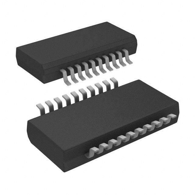
| 描述 | IC LP SERIAL 16-BIT A/D 16-SOIC模数转换器 - ADC Low-Power Serial 16-Bit Sampling |
| 产品分类 | |
| 品牌 | Texas Instruments |
| 产品手册 | |
| 产品图片 |
|
| rohs | 符合RoHS无铅 / 符合限制有害物质指令(RoHS)规范要求 |
| 产品系列 | 数据转换器IC,模数转换器 - ADC,Texas Instruments ADS7813U- |
| 数据手册 | |
| 产品型号 | ADS7813U |
| 产品培训模块 | http://www.digikey.cn/PTM/IndividualPTM.page?site=cn&lang=zhs&ptm=13240 |
| 产品目录页面 | |
| 产品种类 | 模数转换器 - ADC |
| 位数 | 16 |
| 供应商器件封装 | 16-SOIC |
| 信噪比 | 85 dB |
| 分辨率 | 16 bit |
| 制造商产品页 | http://www.ti.com/general/docs/suppproductinfo.tsp?distId=10&orderablePartNumber=ADS7813U |
| 包装 | 管件 |
| 单位重量 | 420.400 mg |
| 商标 | Texas Instruments |
| 安装类型 | 表面贴装 |
| 安装风格 | SMD/SMT |
| 封装 | Tube |
| 封装/外壳 | 16-SOIC(0.295",7.50mm 宽) |
| 封装/箱体 | SOIC-16 |
| 工作温度 | -40°C ~ 85°C |
| 工作电源电压 | 4.75 V to 5.25 V |
| 工厂包装数量 | 40 |
| 接口类型 | Serial SPI |
| 数据接口 | SPI |
| 最大功率耗散 | 35 mW |
| 最大工作温度 | + 85 C |
| 最小工作温度 | - 40 C |
| 标准包装 | 40 |
| 特性 | - |
| 电压参考 | 2.5 V |
| 电压源 | 单电源 |
| 系列 | ADS7813 |
| 结构 | SAR |
| 转换器数 | 1 |
| 转换器数量 | 1 |
| 转换速率 | 40 kS/s |
| 输入数和类型 | 3 个单端,单极3 个单端,双极 |
| 输入类型 | Single-Ended |
| 通道数量 | 1 Channel |
| 采样率(每秒) | 40k |

.jpg)


- 商务部:美国ITC正式对集成电路等产品启动337调查
- 曝三星4nm工艺存在良率问题 高通将骁龙8 Gen1或转产台积电
- 太阳诱电将投资9.5亿元在常州建新厂生产MLCC 预计2023年完工
- 英特尔发布欧洲新工厂建设计划 深化IDM 2.0 战略
- 台积电先进制程称霸业界 有大客户加持明年业绩稳了
- 达到5530亿美元!SIA预计今年全球半导体销售额将创下新高
- 英特尔拟将自动驾驶子公司Mobileye上市 估值或超500亿美元
- 三星加码芯片和SET,合并消费电子和移动部门,撤换高东真等 CEO
- 三星电子宣布重大人事变动 还合并消费电子和移动部门
- 海关总署:前11个月进口集成电路产品价值2.52万亿元 增长14.8%


PDF Datasheet 数据手册内容提取
ADS7813 ADS7813 ADS7813 SBAS043C – MARCH 1997 – REVISED SEPTEMBER 2005 Low-Power, Serial 16-Bit Sampling ANALOG-TO-DIGITAL CONVERTER FEATURES DESCRIPTION (cid:1) 20µs max CONVERSION TIME The ADS7813 is a low-power, single +5V supply, 16-bit (cid:1) SINGLE +5V SUPPLY OPERATION sampling analog-to-digital (A/D) converter. It contains a complete 16-bit capacitor-based SAR A/D with a (cid:1) PIN-COMPATIBLE WITH 12-BIT ADS7812 sample/hold, clock, reference, and serial data interface. (cid:1) EASY-TO-USE SERIAL INTERFACE The converter can be configured for a variety of input ranges (cid:1) 0.3" DIP-16 AND SO-16 including ±10V, ±5V, 0V to 10V, and 0.5V to 4.5V. A high (cid:1) ±2.0LSB max INL impedance 0.3V to 2.8V input range is also available (input (cid:1) 87dB min SINAD impedance > 10MΩ). For most input ranges, the input voltage can swing to +16.5V or –16.5V without damage to (cid:1) USES INTERNAL OR EXTERNAL the converter. REFERENCE A flexible SPI-compatible serial interface allows data to be (cid:1) MULTIPLE INPUT RANGES synchronized to an internal or external clock. The ADS7813 (cid:1) 35mW max POWER DISSIPATION is specified at a 40kHz sampling rate over the –40°C to (cid:1) NO MISSING CODES +85°C temperature range. It is available in a 0.3" DIP-16 or (cid:1) 50µW POWER DOWN MODE an SO-16 package. APPLICATIONS (cid:1) MEDICAL INSTRUMENTATION (cid:1) DATA ACQUISITION SYSTEMS (cid:1) ROBOTICS (cid:1) INDUSTRIAL CONTROL BUSY PWRD CONV CS (cid:1) TEST EQUIPMENT (cid:1) DIGITAL SIGNAL PROCESSING Successive Approximation Register and Control Logic Clock (cid:1) DSP SERVO CONTROL 40kΩ(1) CDAC R1IN 8kΩ(1) EXT/INT R2IN Serial 20kΩ(1) Data DATACLK R3IN Comparator Out BUF DATA Buffer Internal CAP +2.5V Ref 4kΩ(1) NOTE: (1) Actual value may vary ±30%. REF Please be aware that an important notice concerning availability, standard warranty, and use in critical applications of Texas Instruments semiconductor products and disclaimers thereto appears at the end of this data sheet. All trademarks are the property of their respective owners. PRODUCTION DATA information is current as of publication date. Copyright © 1997-2005, Texas Instruments Incorporated Products conform to specifications per the terms of Texas Instruments standard warranty. Production processing does not necessarily include testing of all parameters. www.ti.com
ABSOLUTE MAXIMUM RATINGS(1) ELECTROSTATIC DISCHARGE SENSITIVITY Analog Inputs: R1 .........................................................................±16.5V IN R2 ................................................GND – 0.3V to +16.5V IN R3IN.........................................................................±16.5V This integrated circuit can be damaged by ESD. Texas Instru- REF............................................GND – 0.3V to V + 0.3V S ments recommends that all integrated circuits be handled with CAP...............................................Indefinite Short to GND Momentary Short to V appropriate precautions. Failure to observe proper handling S VS...........................................................................................................7V and installation procedures can cause damage. Digital Inputs......................................................GND – 0.3V to V + 0.3V S Maximum Junction Temperature...................................................+165°C ESD damage can range from subtle performance degradation Internal Power Dissipation.............................................................825mW to complete device failure. Precision integrated circuits may be Lead Temperature (soldering, 10s) ...............................................+300°C more susceptible to damage because very small parametric NOTE: (1) Stresses above these ratings may cause permanent damage. changes could cause the device not to meet its published Exposure to absolute maximum conditions for extended periods may degrade specifications. device reliability. PACKAGE/ORDERING INFORMATION(1) MINIMUM MAXIMUM SPECIFIED SIGNAL-TO- INTEGRAL NO MISSING (NOISE + SPECIFIED LINEARITY CODE LEVEL DISTORTION) PACKAGE TEMPERATURE PACKAGE ORDERING TRANSPORT PRODUCT ERROR (LSB) (LSB) RATIO (DB) PACKAGE-LEAD DESIGNATOR RANGE MARKING NUMBER MEDIA, QUANTITY ADS7813P ±3 15 85 Dip-16 N –40°C to +85°C ADS7813P ADS7813P Tubes, 25 ADS7813PB ±2 16 87 " " " ADS7813PB ADS7813PB Tubes, 25 ADS7813U ±3 15 85 SO-16 DW –40°C to +85°C ADS7813U ADS7813U Tubes, 48 " " " " " " " " ADS7813U/1K Tape and Reel, 1000 ADS7813UB ±2 16 87 SO-16 DW –40°C to +85°C ADS7813UB ADS7813UB Tubes, 48 " " " " " " " " ADS7813UB/1K Tape and Reel, 1000 NOTE: (1) For the most current package and ordering information, see the Package Option Addendum at the end of this data sheet, or see the TI web site at www.ti.com. ELECTRICAL CHARACTERISTICS At T = –40°C to +85°C, f = 40kHz, V = +5V ±5%, using internal reference, unless otherwise specified. A S S ADS7813P, U ADS7813PB, UB PARAMETER CONDITIONS MIN TYP MAX MIN TYP MAX UNITS RESOLUTION 16 ✻ Bits ANALOG INPUT Voltage Range See Table I ✻ Impedance See Table I ✻ Capacitance 35 ✻ pF THROUGHPUT SPEED Conversion Time 20 ✻ µs Complete Cycle Acquire and Convert 25 ✻ µs Throughput Rate 40 ✻ kHz DC ACCURACY Integral Linearity Error ±3 ✻ ±2 LSB(1) Differential Linearity Error +3, –2 ✻ +2, –1 LSB No Missing Codes 15 16 Bits Transition Noise(2) 0.6 ✻ LSB Full Scale Error(3) ±0.5 ±0.25 % Full Scale Error Drift ±14 ✻ ppm/°C Full Scale Error(3) Ext. 2.5000V Ref ±0.5 ±0.25 % Full Scale Error Drift Ext. 2.5000V Ref ±5 ✻ ppm/°C Bipolar Zero Error Bipolar Ranges ±10 ✻ mV Bipolar Zero Error Drift Bipolar Ranges ±3 ✻ ppm/°C Unipolar Zero Error Unipolar Ranges ±6 ✻ mV Unipolar Zero Error Drift Unipolar Ranges ±3 ✻ ppm/°C Recovery Time to Rated Accuracy 1.0µF Capacitor to CAP 300 ✻ µs from Power Down(4) Power Supply Sensitivity +4.75V < (V = +5V) < +5.25 ±12 ✻ LSB S AC ACCURACY Spurious-Free Dynamic Range f = 1kHz 90 100 96 102 dB(5) IN Total Harmonic Distortion f = 1kHz –98 –90 –100 –96 dB IN Signal-to-(Noise+Distortion) f = 1kHz 85 89 87 ✻ dB IN Signal-to-Noise f = 1kHz 85 89 87 ✻ dB IN Useable Bandwidth(6) 130 ✻ kHz Full Power –3dB Bandwidth 600 ✻ kHz ADS7813 2 www.ti.com SBAS043C
ELECTRICAL CHARACTERISTICS (Cont.) At T = –40°C to +85°C, f = 40kHz, V = +5V ±5%, using internal reference, unless otherwise specified. A S S ADS7813P, U ADS7813PB, UB PARAMETER CONDITIONS MIN TYP MAX MIN TYP MAX UNITS SAMPLING DYNAMICS Aperture Delay 40 ✻ ns Aperture Jitter 20 ✻ ps Transient Response FS Step 5 ✻ µs Overvoltage Recovery(7) 750 ✻ ns REFERENCE Internal Reference Voltage 2.48 2.5 2.52 ✻ ✻ ✻ V Internal Reference Source Current 100 ✻ µA Internal Reference Drift 8 ✻ ppm/°C External Reference Voltage Range 2.3 2.5 2.7 ✻ ✻ ✻ V External Reference Current Drain V = +2.5V 100 ✻ µA REF CAP Compensation Capacitors ESR(8) 3 ✻ Ω DIGITAL INPUTS Logic Levels V –0.3 +0.8 ✻ ✻ V IL V (9) +2.0 V +0.3V ✻ ✻ V IH S I ±10 ✻ µA IL I ±10 ✻ µA IH DIGITAL OUTPUTS Serial Data Format Binary Two’s Complement Data Coding V I = 1.6mA +0.4 ✻ V OL SINK V I = 500µA +4 ✻ V OH SOURCE Leakage Current High-Z State, ±1 ✻ µA V = 0V to V OUT S Output Capacitance High-Z State 15 15 pF POWER SUPPLY V +4.75 +5 +5.25 ✻ ✻ ✻ V S Power Dissipation f = 40kHz 35 ✻ mW S TEMPERATURE RANGE Specified Performance –40 +85 ✻ ✻ °C Derated Performance –55 +125 ✻ ✻ °C ✻ Same specification as grade to the left. NOTES:(1) LSB means Least Significant Bit. For the ±10V input range, one LSB is 305µV. (2) Typical rms noise at worst case transitions and temperatures. (3) Full scale error is the worst case of –Full Scale or +Full Scale untrimmed deviation from ideal first and last code transitions, divided by the transition voltage (not divided by the full-scale range) and includes the effect of offset error. (4) After the ADS7813 is initially powered on and fully settles, this is the time delay after it is brought out of Power Down Mode until all internal settling occurs and the analog input is acquired to rated accuracy, and normal conversions can begin again. (5) All specifications in dB are referred to a full-scale input. (6) Useable Bandwidth defined as Full-Scale input frequency at which Signal-to-(Noise+Distortion) degrades to 60dB, or 10 bits of accuracy. (7) Recovers to specified performance after 2 x FS input overvoltage. (8) ESR = total equivalent series resistance for the compensation capacitors. (9) The minimum V level for the DATACLK signal is 3V. IH ADS7813 3 SBAS043C www.ti.com
PIN CONFIGURATION PIN # NAME DESCRIPTION 1 R1 Analog Input. See Tables I and IV. IN 2 GND Ground 3 R2 Analog Input. See Tables I and IV. IN 4 R3 Analog Input. See Tables I and IV. IN 5 BUF Reference Buffer Output. Connect to R1 , R2 , or R3 , as needed. IN IN IN 6 CAP Reference Buffer Compensation Node. Decouple to ground with a 1µF tantalum capacitor in parallel with a 0.01µF ceramic capacitor. 7 REF Reference Input/Output. Outputs internal +2.5V reference via a series 4kΩ resistor. Decouple this voltage with a 1µF to 2.2µF tantalum capacitor to ground. If an external reference voltage is applied to this pin, it will override the internal reference. 8 GND Ground 9 DATACLK Data Clock Pin. With EXT/INT LOW, this pin is an output and provides the synchronous clock for the serial data. The output is tri-stated when CS is HIGH. With EXT/INT HIGH, this pin is an input and the serial data clock must be provided externally. 10 DATA Serial Data Output. The serial data is always the result of the last completed conversion and is synchronized to DATACLK. If DATACLK is from the internal clock (EXT/INT LOW), the serial data is valid on both the rising and falling edges of DATACLK. DATA is tri-stated when CS is HIGH. 11 EXT/INT External or Internal DATACLK Pin. Selects the source of the synchronous clock for serial data. If HIGH, the clock must be provided externally. If LOW, the clock is derived from the internal conversion clock. Note that the clock used to time the conversion is always internal regardless of the status of EXT/INT. 12 CONV Convert Input. A falling edge on this input puts the internal sample/hold into the hold state and starts a conversion regardless of the state of CS. If a conversion is already in progress, the falling edge is ignored. If EXT/INT is LOW, data from the previous conversion will be serially transmitted during the current conversion. 13 CS Chip Select. This input tri-states all outputs when HIGH and enables all outputs when LOW. This includes DATA, BUSY, and DATACLK (when EXT/INT is LOW). Note that a falling edge on CONV will initiate a conversion even when CS is HIGH. 14 BUSY Busy Output. When a conversion is started, BUSY goes LOW and remains LOW throughout the conversion. If EXT/INT is LOW, data is serially transmitted while BUSY is LOW. BUSY is tri-stated when CS is HIGH. 15 PWRD Power Down Input. When HIGH, the majority of the ADS7813 is placed in a low power mode and power consumption is significantly reduced. CONV must be taken LOW prior to PWRD going LOW in order to achieve the lowest power consumption. The time required for the ADS7813 to return to normal operation after power down depends on a number of factors. Consult the Power Down section for more information. 16 V +5V Supply Input. For best performance, decouple to ground with a 0.1µF ceramic capacitor in parallel with a 10µF tantalum S capacitor. PIN CONFIGURATION ANALOG CONNECT CONNECT CONNECT INPUT INPUT R1 R2 R3 IMPEDANCE IN IN IN Top View DIP, SOIC RANGE (V) TO TO TO (kΩ) ±10V V BUF GND 45.7 IN 0.3125V to 2.8125V V V V > 10,000 IN IN IN ±5V GND BUF V 26.7 IN R1IN 1 16 VS 0V to 10V BUF GND VIN 26.7 GND 2 15 PWRD 0V to 4V BUF VIN GND 21.3 ±3.33V V BUF V 21.3 R2 3 14 BUSY IN IN IN 0.5V to R3IN 4 13 CS 4.5V GND VIN GND 21.3 ADS7813 BUF 5 12 CONV TABLE I. ADS7813 Input Ranges. CAP 6 11 EXT/INT REF 7 10 DATA GND 8 9 DATACLK ADS7813 4 www.ti.com SBAS043C
TYPICAL PERFORMANCE CURVES At T = +25°C, f = 40kHz, V = +5V, ±10V input range, using internal reference, unless otherwise noted. A S S FREQUENCY SPECTRUM FREQUENCY SPECTRUM (8192 Point FFT; f = 980Hz, 0dB) (8192 Point FFT; f = 9.8kHz, 0dB) IN IN 0 0 –20 –20 –40 –40 B) B) e (d –60 e (d –60 d d plitu –80 plitu –80 m m A –100 A –100 –120 –120 –140 –140 0 5 10 15 20 0 5 10 15 20 Frequency (kHz) Frequency (kHz) SNR AND SINAD vs TEMPERATURE SFDR AND THD vs TEMPERATURE (f = 1kHz, 0dB) (f = 1kHz, 0dB) IN IN 92 106 –106 91 105 –105 B) SNR SFDR R and SINAD (d 988098 SINAD SFDR (dB) 111000432 THD –––111000432 THD (dB) N S 87 101 –101 86 100 –100 –50 –25 0 25 50 75 100 –50 –25 0 25 50 75 100 Temperature (°C) Temperature (°C) SIGNAL-TO-(NOISE + DISTORTION) INTERNAL REFERENCE VOLTAGE vs INPUT FREQUENCY (f = 0dB) vs TEMPERATURE IN 90 2.515 89 2.510 88 V) e ( 2.505 B) nc d 87 e SINAD ( 8865 ernal Refer 22..540905 nt I 84 2.490 83 2.485 100 1k 10k 20k –50 –25 0 25 50 75 100 Input Signal Frequency (Hz) Temperature (°C) ADS7813 5 SBAS043C www.ti.com
TYPICAL PERFORMANCE CURVES (Cont.) At T = +25°C, f = 40kHz, V = +5V, ±10V input range, using internal reference, unless otherwise noted. A S S ILE AND DLE AT –40°C ILE AND DLE AT +25°C 2 2 B) 1 B) 1 S S L 0 L 0 E ( E ( IL –1 IL –1 –2 –2 2 2 B) 1 B) 1 S S E (L 0 E (L 0 DL –1 DL –1 –2 –2 8000h C000h 0000h 4000h 7FFFh 8000h C000h 0000h 4000h 7FFFh Hex BTC Code Hex BTC Code POWER SUPPLY RIPPLE SENSITIVITY ILE AND DLE AT +85°C ILE/DLE DEGRADATION PER LSB OF P-P RIPPLE 2 1 B) 1 B) LS 0 LS 10–1 ILE ( –1 n (LSB/ 10–2 –2 atio ILE d 2 a gr 10–3 e SB) 1 y D E (L 0 earit 10–4 L n D –1 Li DLE –2 10–5 8000h C000h 0000h 4000h 7FFFh 101 102 103 104 105 106 107 Hex BTC Code Power Supply Ripple Frequency (Hz) WORST-CASE INL vs ESR OF REFERENCE BUFFER COMPENSATION CAPACITOR 35 30 B) S L (L 25 N e I 20 s a C st- 15 or W 10 5 0 1.5 2 2.5 3 3.5 4 4.5 5 5.5 6 6.5 7 7.5 8 8.5 9 Capacitor ESR (Ω) ADS7813 6 www.ti.com SBAS043C
BASIC OPERATION EXTERNAL DATACLK Figure 1b shows a basic circuit to operate the ADS7813 with INTERNAL DATACLK a ±10V input range. To begin a conversion, a falling edge Figure 1a shows a basic circuit to operate the ADS7813 with must be provided to the CONV input. BUSY will go LOW a ±10V input range. To begin a conversion and serial indicating that a conversion has started and will stay LOW transmission of the results from the previous conversion, a until the conversion is complete. Just prior to BUSY rising falling edge must be provided to the CONV input. BUSY near the end of the conversion, the internal working register will go LOW indicating that a conversion has started and holding the conversion result will be transferred to the will stay LOW until the conversion is complete. During the internal shift register. conversion, the results of the previous conversion will be The internal shift register is clocked via the DATACLK transmitted via DATA while DATACLK provides the syn- input. The recommended method of reading the conversion chronous clock for the serial data. The data format is 16-bit, result is to provide the serial clock after the conversion has Binary Two’s Complement, and MSB first. Each data bit is completed. See External DATACLK under the Reading valid on both the rising and falling edge of DATACLK. Data section of this data sheet for more information. BUSY is LOW during the entire serial transmission and can be used as a frame synchronization signal. C C 1 2 ADS7813 0.1µF 10µF ±10V 1 R1IN VS 16 + +5V 2 GND PWRD 15 3 R2 BUSY 14 Frame Sync (optional) IN 4 R3 CS 13 IN 5 BUF CONV 12 Convert Pulse C + C 3 4 6 CAP EXT/INT 11 1µF 0.01µF C5 + 7 REF DATA 10 40ns min 1µF 8 GND DATACLK 9 FIGURE 1a. Basic Operation, ±10V Input Range, Internal DATACLK. C C 1 2 ADS7813 0.1µF 10µF ±10V 1 R1IN VS 16 + +5V 2 GND PWRD 15 3 R2 BUSY 14 Interrupt (optional) IN 4 R3 CS 13 Chip Select (optional(1)) IN Convert Pulse 5 BUF CONV 12 C + C 3 4 6 CAP EXT/INT 11 +5V 1µF 0.01µF C + 7 REF DATA 10 40ns min 5 1µF 8 GND DATACLK 9 External Clock NOTE: (1) Tie CS to GND if the outputs will always be active. FIGURE 1b. Basic Operation, ±10V Input Range, External DATACLK. ADS7813 7 SBAS043C www.ti.com
STARTING A CONVERSION SYMBOL DESCRIPTION MIN TYP MAX UNITS t1 Conversion Plus Acquisition Time 25 µs If a conversion is not currently in progress, a falling edge on t2 CONV LOW to All Digital 8 µs the CONV input places the sample and hold into the hold Inputs Stable mode and begins a conversion, as shown in Figure 2 and t CONV LOW to Initiate a Conversion 40 ns 3 with the timing given in Table II. During the conversion, the t BUSY Rising to Any Digital 0 ns 4 CONV input is ignored. Starting a conversion does not Input Active t CONV HIGH Prior to Start 2 µs depend on the state of CS. A conversion can be started once 5 of Conversion every 25µs (40kHz maximum conversion rate). There is no t BUSY LOW 19 20 µs minimum conversion rate. 6 t7 CONV LOW to BUSY LOW 85 120 ns Even though the CONV input is ignored while a conversion t8 Aperture Delay 40 ns is in progress, this input should be held static during the t9 Conversion Time 18 20 µs conversion period. Transitions on this digital input can t10 Conversion Complete to 1.1 2 µs easily couple into sensitive analog portions of the converter, BUSY Rising adversely affecting the conversion results (see the Sensitiv- t Acquisition Time 5 µs 11 ity to External Digital Signals section of this data sheet for t CONV LOW to Rising Edge 1.4 µs 12 more information). of First DATACLK t Internal DATACLK HIGH 250 350 500 ns Ideally, the CONV input should go LOW and remain LOW 13 t Internal DATACLK LOW 600 760 875 ns throughout the conversion. It should return HIGH sometime 14 t Internal DATACLK Period 1.1 µs after BUSY goes HIGH. In addition, it should be HIGH 15 t DATA Valid to Internal 20 ns prior to the start of the next conversion for a minimum time 16 DATACLK Rising period given by t . This will ensure that the digital transition 5 t17 Internal DATACLK Falling 400 ns on the CONV input will not affect the signal that is acquired to DATA Not Valid for the next conversion. t Falling Edge of Last DATACLK 800 ns 18 to BUSY Rising An acceptable alternative is to return the CONV input HIGH t External DATACLK Rising 15 ns as soon after the start of the conversion as possible. For 19 to DATA Not Valid example, a negative going pulse 100ns wide would make a t20 External DATACLK Rising 55 85 ns good CONV input signal. It is strongly recommended that to DATA Valid from time t after the start of a conversion until BUSY rises, t External DATACLK HIGH 50 ns 2 21 the CONV input should be held static (either HIGH or t External DATACLK LOW 50 ns 22 LOW). During this time, the converter is more sensitive to t External DATACLK Period 100 ns 23 external noise. t CONV LOW to External 100 ns 24 DATACLK Active t External DATACLK LOW 2 µs 25 or CS HIGH to BUSY Rising t CS LOW to Digital Outputs Enabled 85 ns 26 t CS HIGH to Digital Outputs Disabled 85 ns 27 TABLE II. ADS7813 Timing. T = –40°C to +85°C. A t 1 t 2 t t t 3 4 5 CONV t 6 t 7 BUSY t t 8 10 t9 t11 MODE Acquire Convert Acquire Convert FIGURE 2. Basic Conversion Timing. ADS7813 8 www.ti.com SBAS043C
DESCRIPTION ANALOG INPUT DIGITAL OUTPUT BINARY TWO’S COMPLEMENT Full-Scale Range ±10V 0.5V to 4.5V Least Significant Bit (LSB) 305µV 61µV BINARY CODE HEX CODE +Full Scale –1LSB 9.999695V 4.499939V 0111 1111 1111 1111 7FFF Midscale 0V 2.5V 0000 0000 0000 0000 0000 Midscale –1LSB –305µV 2.499939µV 1111 1111 1111 1111 FFFF –Full Scale –10V 0.5V 10000 0000 0000 0000 8000 TABLE III. Ideal Input Voltage and Corresponding Digital Output for Two Common Input Ranges. Converter Core REF CDAC CONV Clock Control Logic BUSY Each flip-flop in the working register is latched as the conversion proceeds Working Register D Q D Q D Q D Q D Q ••• W0 W1 W2 W14 W15 Update of the shift register occurs just prior to BUSY Rising(1) Shift Register D Q D Q D Q D Q D Q D Q DATA EXT/INT S0 S1 S2 S14 S15 SOUT Delay DATACLK CS NOTE: (1) If EXT/INT is HIGH (external clock), DATACLK is HIGH, and CS is LOW during this time, the shift register will not be updated and the conversion result will be lost. FIGURE 3. Block Diagram of the ADS7813’s Digital Inputs and Outputs. READING DATA The ADS7813 digital output is in Binary Two’s Comple- CONV ment (BTC) format. Table III shows the relationship be- tween the digital output word and the analog input voltage t 25 under ideal conditions. t – t 6 25 Figure 3 shows the relationship between the various digital BUSY inputs, digital outputs, and internal logic of the ADS7813. Figure 4 shows when the internal shift register of the NOTE: Update of the internal shift register occurs in the ADS7813 is updated and how this relates to a single conver- shaded region. If EXT/INT is HIGH, then DATACLK must be LOW or CS must be HIGH during this time. sion cycle. Together, these two figures point out a very important aspect of the ADS7813: the conversion result is not available until after the conversion is complete. The FIGURE 4. Timing of the Shift Register Update. implications of this are discussed in the following sections. ADS7813 9 SBAS043C www.ti.com
INTERNAL DATACLK EXTERNAL DATACLK With EXT/INT tied LOW, the result from conversion ‘n’ is With EXT/INT tied HIGH, the result from conversion ‘n’ is serially transmitted during conversion ‘n+1’, as shown in clocked out after the conversion has completed, during the Figure 5 and with the timing given in Table II. Serial next conversion (‘n+1’), or a combination of these two. transmission of data occurs only during a conversion. When Figure 6 shows the case of reading the conversion result a transmission is not in progress, DATA and DATACLK are after the conversion is complete. Figure 7 describes reading LOW. the result during the next conversion. Figure 8 combines the During the conversion, the results of the previous conver- important aspects of Figures 6 and 7 as to reading part of the sion will be transmitted via DATA, while DATACLK result after the conversion is complete and the remainder provides the synchronous clock for the serial data. The data during the next conversion. format is 16-bit, Binary Two’s Complement, and MSB first. The serial transmission of the conversion result is initiated Each data bit is valid on both the rising and falling edges of by a rising edge on DATACLK. The data format is 16-bit, DATACLK. BUSY is LOW during the entire serial trans- Binary Two’s Complement, and MSB first. Each data bit is mission and can be used as a frame synchronization signal. valid on the falling edge of DATACLK. In some cases, it t 1 CONV BUSY t 13 t12 t15 t18 DATACLK 1 2 3 14 15 16 1 t t 16 14 t 17 DATA MSB Bit 14 Bit 13 Bit 2 Bit 1 LSB MSB FIGURE 5. Serial Data Timing, Internal Clock (EXT/INT and CS LOW). t 1 t 5 CONV BUSY t 21 t t 4 23 DATACLK 1 2 3 4 14 15 16 t t 19 22 t 20 DATA MSB Bit 14 Bit 13 Bit 2 Bit 1 LSB FIGURE 6. Serial Data Timing, External Clock, Clocking After the Conversion Completes (EXT/INT HIGH, CS LOW). ADS7813 10 www.ti.com SBAS043C
might be possible to use the rising edge of the DATACLK completed and before the next conversion starts—as shown signal. However, one extra clock period (not shown in in Figure 6. Note that the DATACLK signal should be static Figures 6, 7, and 8) is needed for the final bit. before the start of the next conversion. If this is not ob- served, the DATACLK signal could affect the voltage that The external DATACLK signal must be LOW or CS must is acquired. be HIGH prior to BUSY rising (see time t in Figures 7 and 25 8). If this is not observed during this time, the output shift register of the ADS7813 will not be updated with the External DATACLK Active During the Next Conversion conversion result. Instead, the previous contents of the shift Another method of obtaining the conversion result is shown register will remain and the new result will be lost. in Figure 7. Since the output shift register is not updated Before reading the next three paragraphs, consult the Sensi- until the end of the conversion, the previous result remains tivity to External Digital Signals section of this data sheet. valid during the next conversion. If a fast clock (≥ 2MHz) This will explain many of the concerns regarding how and can be provided to the ADS7813, the result can be read when to apply the external DATACLK signal. during time t . During this time, the noise from the 2 DATACLK signal is less likely to affect the conversion result. External DATACLK Active After the Conversion The preferred method of obtaining the conversion result is to provide the DATACLK signal after the conversion has been t 1 t 2 CONV BUSY t 21 t t t 24 23 25 DATACLK 1 2 3 4 15 16 1 t t 19 22 t 20 DATA MSB Bit 14 Bit 13 Bit 1 LSB MSB FIGURE 7. Serial Data Timing, External Clock, Clocking During the Next Conversion (EXT/INT HIGH, CS LOW). CONV BUSY t 5 t t t 4 24 25 DATACLK 1 2 n n+1 15 16 DATA MSB Bit 14 Bit n Bit n-1 Bit 1 LSB FIGURE 8. Serial Data Timing, External Clock, Clocking After the Conversion Completes and During the Next Conversion (EXT/INT HIGH, CS LOW). ADS7813 11 SBAS043C www.ti.com
External DATACLK Active After the Conversion CHIP SELECT (CS) and During the Next Conversion The CS input allows the digital outputs of the ADS7813 to Figure 8 shows a method that is a hybrid of the two previous be disabled and gates the external DATACLK signal when approaches. This method works very well for microcontrollers EXT/INT is HIGH. See Figure 9 for the enable and disable that do serial transfers 8 bits at a time and for slower time associated with CS and Figure 3 for a block diagram of microcontrollers. For example, if the fastest serial clock that the ADS7813’s logic. The digital outputs can be disabled at the microcontroller can produce is 1µs, the approach shown any time. in Figure 6 would result in a diminished throughput (26kHz Note that a conversion is initiated on the falling edge of maximum conversion rate). The method described in Figure CONV even if CS is HIGH. If the EXT/INT input is LOW 7 could not be used without risk of affecting the conversion (internal DATACLK) and CS is HIGH during the entire result (the clock would have to be active after time t2). The conversion, the previous conversion result will be lost (the approach in Figure 8 results in an improved throughput rate serial transmission occurs but DATA and DATACLK are (33kHz maximum with a 1µs clock) and DATACLK is not disabled). active after time t . 2 COMPATIBILITY WITH THE ADS7812 CS The only difference between the ADS7812 and the ADS7813 is in the internal control logic and the digital interface. Since t26 t27 the ADS7812 is a 12-bit converter, the internal shift register BUSY, DATA, HI-Z Active HI-Z DATACLK(1) is 12 bits wide. In addition, only 12-bit decisions are made during the conversion. Thus, the ADS7812’s conversion NOTE: (1) DATACLK is an output only when EXT/INT is LOW. time is approximately 75% of the ADS7813’s. FIGURE 9. Enable and Disable Timing for Digital Outputs. In the internal DATACLK mode, the ADS7812 produces 12 DATACLK periods during the conversion instead of the ANALOG INPUT ADS7813’s 16 (see Figure 5). In the external DATACLK mode, the ADS7812 can accept 16 clock periods on The ADS7813 offers a number of input ranges. This is DATACLK. At the start of the 13th clock cycle, the DATA accomplished by connecting the three input resistors to output will go LOW and remain LOW. Thus, Figures 6, 7, either the analog input (V ), to ground (GND), or to the IN 8, and the associated times in Table II can also be used for 2.5V reference buffer output (BUF). Table I shows the input the ADS7812, but the last four bits of the conversion result ranges that are typically used in most data acquisition will be zero. applications. These ranges are all specified to meet the specifications given in the Specifications table. Table IV contains a complete list of ideal input ranges, associated input connections, and comments regarding the range. ANALOG CONNECT CONNECT CONNECT INPUT INPUT R1 R2 R3 IMPEDANCE IN IN IN RANGE (V) TO TO TO (kΩ) COMMENT 0.3125 to 2.8125 V V V > 10,000 Specified offset and gain IN IN IN –0.417 to 2.916 V V BUF 26.7 V cannot go below GND – 0.3V IN IN IN 0.417 to 3.750 V V GND 26.7 Offset and gain not specified IN IN ±3.333 V BUF V 21.3 Specified offset and gain IN IN –15 to 5 V BUF BUF 45.7 Offset and gain not specified IN ±10 V BUF GND 45.7 Specified offset and gain IN 0.833 to 7.5 V GND V 21.3 Offset and gain not specified IN IN –2.5 to 17.5 V GND BUF 45.7 Exceeds absolute maximum V IN IN 2.5 to 22.5 V GND GND 45.7 Exceeds absolute maximum V IN IN 0 to 2.857 BUF V V 45.7 Offset and gain not specified IN IN –1 to 3 BUF V BUF 21.3 V cannot go below GND – 0.3V IN IN 0 to 4 BUF V GND 21.3 Specified offset and gain IN –6.25 to 3.75 BUF BUF V 26.7 Offset and gain not specified IN 0 to 10 BUF GND V 26.7 Specified offset and gain IN 0.357 to 3.214 GND V V 45.7 Offset and gain not specified IN IN –0.5 to 3.5 GND V BUF 21.3 V cannot go below GND – 0.3V IN IN 0.5 to 4.5 GND V GND 21.3 Specified offset and gain IN ±5 GND BUF V 26.7 Specified offset and gain IN 1.25 to 11.25 GND GND V 26.7 Offset and gain not specified IN TABLE IV. Complete List of Ideal Input Ranges. ADS7813 12 www.ti.com SBAS043C
The input impedance results from the various connections and with slower amplifiers. Be very careful with single-supply the internal resistor values (refer to the block diagram on the amplifiers, particularly if their output will be required to front page of this data sheet). The internal resistor values are swing very close to the supply rails. typical and can change by ±30%, due to process variations. In addition, be careful in regards to the amplifier linearity. The However, the ratio matching of the resistors is considerably outputs of single-supply and rail-to-rail amplifiers can satu- better than this. Thus, the input range will vary only a few rate as they approach the supply rails. Rather than the ampli- tenths of a percent from part to part, while the input imped- fier transfer function being a straight line, the curve can ance can vary up to ±30%. become severely ‘S’ shaped. Also, watch for the point where The Specifications table contains the maximum limits for the the amplifier switches from sourcing current to sinking cur- variation of the analog input range, but only for those ranges rent. For some amplifiers, the transfer function can be notice- where the comment field shows that the offset and gain are ably discontinuous at this point, causing a significant change specified (this includes all the ranges listed in Table I). For the in the output voltage for a much smaller change on the input. other ranges, the offset and gain are not tested and are not Texas Instruments manufactures a wide variety of operational specified. and instrumentation amplifiers that can be used to drive the Five of the input ranges in Table IV are not recommended for input of the ADS7813. These include the OPA627, OPA132, general use. The upper-end of the –2.5V to +17.5V range and and INA110. +2.5V to +22.5V range exceed the absolute maximum analog input voltage. These ranges can still be used as long as the input voltage remains under the absolute maximum, but this REFERENCE will moderately to significantly reduce the full-scale range of The ADS7813 can be operated with its internal 2.5V refer- the converter. ence or an external reference. By applying an external refer- Likewise, three of the input ranges involve the connection at ence voltage to the REF pin, the internal reference voltage is R2 being driven below GND. This input has a reverse- IN overdriven. The voltage at the REF input is internally buffered biased ESD protection diode connection to ground. If R2 is IN by a unity gain buffer. The output of this buffer is present at taken below GND – 0.3V, this diode will be forward-biased the BUF and CAP pins. and will clamp the negative input at –0.4V to –0.7V, depend- ing on the temperature. Since the negative full-scale value of REF these input ranges exceed –0.4V, they are not recommended. The REF pin is the output of the internal 2.5V reference or the Note that Table IV assumes that the voltage at the REF pin is input for an external reference. A 1µF to 2.2µF tantulum +2.5V. This is true if the internal reference is being used or if capacitor should be connected between this pin and ground. the external reference is +2.5V. Other reference voltages will The capacitor should be placed as close to the ADS7813 as change the values in Table IV. possible. When using the internal reference, the REF pin should not be HIGH IMPEDANCE MODE connected to any type of significant load. An external load When R1 , R2 , and R3 are connected to the analog input, IN IN IN will cause a voltage drop across the internal 4kΩ resistor that the input range of the ADS7813 is 0.3125V to 2.8125V and the is in series with the internal reference. Even a 40MΩ external input impedance is greater than 10MΩ. This input range can be load to ground will cause a decrease in the full-scale range of used to connect the ADS7813 directly to a wide variety of the converter by 6 LSBs. sensors. Figure 10 shows the impedance of the sensor versus the change in ILE and DLE of the ADS7813. The performance of the ADS7813 can be improved for higher sensor impedance by allowing more time for acquisition. For example, 10µs of LINEARITY ERROR vs SOURCE IMPEDANCE 10 acquisition time will approximately double sensor impedance 9 T = +25°C for the same ILE/DLE performance. A Acquisition Time = 5µs 8 DLE The input impedance and capacitance of the ADS7813 are aseBs) 7 vstAtheeemDanrnysSpo ae7srt r8 afaa1ebtswu3l er.w e pwI,efe l itrltthc,hh ee et tnh ewstem eo ognprvsrseeator-rparc httaihu smerseeh p e.ioe nmAwdspasunsner uedcinmdea nitFvnceaiemggr iustpehhreseao r tasu 1ittlguh0dnri sewib f ieiriscla luatn rnsvguetaeeldry yo.o ffw l ettihhsthees Change in Worst-CLinearity Error (LS 6543 ILE 2 1 DRIVING THE ADS7813 ANALOG INPUT 0 In general, any reasonably fast, high-quality operational or 0 1 2 3 4 5 6 7 8 9 10 11 12 13 14 15 instrumentation amplifier can be used to drive the ADS7813 External Source Impedance (kΩ) input. When the converter enters the acquisition mode, there is some charge injection from the converter input to the FIGURE 10.Linearity Error vs Source Impedance in the High amplifier output. This can result in inadequate settling time Impedance Mode (R1 = R2 = R3 = V ). IN IN IN IN ADS7813 13 SBAS043C www.ti.com
The range for the external reference is 2.3V to 2.7V. The power-down mode, CONV is taken HIGH and then PWRD voltage on REF determines the full-scale range of the con- is taken LOW. Note that a conversion will be initiated if verter and the corresponding LSB size. Increasing the refer- PWRD is taken HIGH while CONV is LOW. ence voltage will increase the LSB size in relation to the While in the power-down mode, the voltage on the capaci- internal noise sources which, in turn, can improve signal-to- tors connected to CAP and REF will begin to leak off. The noise ratio. Likewise, decreasing the reference voltage will voltage on the CAP capacitor leaks off much more rapidly reduce the LSB size and signal-to-noise ratio. than on the REF capacitor (the REF input of the ADS7813 becomes high-impedance when PWRD is HIGH—this is not CAP true for the CAP input). When the power-down mode is The CAP pin is used to compensate the internal reference exited, these capacitors must be allowed to recharge and buffer. A 1µF tantalum capacitor in parallel with a 0.01µF settle to a 16-bit level. Figure 11 shows the amount of time ceramic capacitor should be connected between this pin and typically required to obtain a valid 16-bit result based on the ground, with the ceramic capacitor placed as close to the amount of time spent in power down (at room temperature). ADS7813 as possible. The total value of the capacitance on This figure assumes that the total capacitance on the CAP the CAP pin is critical to optimum performance of the pin is 1.01µF. ADS7813. A value larger than 2.0µF could overcompensate Figure 12 provides a circuit which can significantly reduce the buffer while a value lower than 0.5µF may not provide the power up time if the power down time will be fairly brief adequate compensation. The ESR (equivalent series resis- (a few seconds or less). A low on-resistance MOSFET is tance) of these compensation capacitors is also critical. Keep used to disconnect the capacitance on the CAP pin from the the total ESR under 3Ω. See the Typical Characteristic curve, leakage paths internal to the ADS7813. This allows the |Worst-Case INL| vs ESR of Reference Buffer Compensation capacitors to retain their charge for a much longer period of Capacitor, for how the worst-case INL is affected by ESR. time, reducing the time required to recharge them at power up. With this circuit, the power-down time can be extended BUF to tens or hundreds of milliseconds with almost instanta- neous power up. The voltage on the BUF pin is the output of the internal reference buffer. This pin is used to provide +2.5V to the analog input or inputs for the various input configurations. POWER-DOWN TO POWER-UP RESPONSE 300 Texhtee rBnaUl Flo aodu.t pTuhte claona dp srhoovuidlde buep ctoon s1tmanAt aos fa cvuarrrieanbtl et olo aand cy (µs) 250 TA = +25°C could affect the conversion result by modulating the BUF ura c voltage. Also note that the BUF output will show significant Ac 200 glitches as each bit decision is made during a conversion. ed Between conversions, the BUF output is quiet. Rat 150 o e t m 100 Ti POWER DOWN p U er- 50 The ADS7813 has a power-down mode that is activated by ow P taking CONV LOW and then PWRD HIGH. This will 0 0.1 1 10 100 power down all of the analog circuitry including the refer- ence, reducing power dissipation to under 50µW. To exit the Power-Down Duration (ms) FIGURE 11. Power-Down to Power-Up Response. 1RF7604 1 8 1 R1 V 16 IN S 2 7 2 GND PWRD 15 Power-Down Signal 3 6 3 R2 BUSY 14 IN 4 5 4 R3 CS 13 IN 5 BUF CONV 12 + 1µF 0.01µF 6 CAP EXT/INT 11 7 REF DATA 10 8 GND DATACLK 9 FIGURE 12. Improved Power-Up Response Circuit. ADS7813 14 www.ti.com SBAS043C
LAYOUT For example, the timing diagram in Figure 2 shows that the CONV signal should return HIGH sometime during time t . 2 The ADS7813 should be treated as a precision analog In fact, the CONV signal can return HIGH at any time component and should reside completely on the analog during the conversion. However, after time t , the transition 2 portion of the printed circuit board. Ideally, a ground plane of the CONV signal has the potential of creating a good deal should extend underneath the ADS7813 and under all other of noise on the ADS7813 die. If this transition occurs at just analog components. This plane should be separate from the precisely the wrong time, the conversion results could be digital ground until they are joined at the power supply affected. In a similar manner, transitions on the DATACLK connection. This will help prevent dynamic digital ground input could affect the conversion result. currents from modulating the analog ground through a For the ADS7813, there are 16 separate bit decisions which common impedance to power ground. are made during the conversion. The most significant bit The +5V power should be clean, well-regulated, and sepa- decision is made first, proceeding to the least significant bit rate from the +5V power for the digital portion of the design. at the end of the conversion. Each bit decision involves the One possibility is to derive the +5V supply from a linear assumption that the bit being tested should be set. This is regulator located near the ADS7813. If derived from the combined with the result that has been achieved so far. The digital +5V power, a 5Ω to 10Ω resistor should be placed in converter compares this combined result with the actual series with the power connection from the digital supply. It input voltage. If the combined result is too high, the bit is may also be necessary to increase the bypass capacitance cleared. If the result is equal to or lower than the actual input near the VS pin (an additional 100µF or greater capacitor in voltage, the bit remains HIGH. This is why the basic parallel with the 10µF and 0.1µF capacitors). For designs architecture is referred to as successive approximation with a large number of digital components or very high register (SAR). speed digital logic, this simple power supply filtering scheme If the result so far is getting very close to the actual input may not be adequate. voltage, then the comparison involves two voltages which are very close together. The ADS7813 has been designed so that SENSITIVITY TO EXTERNAL the internal noise sources are at a minimum just prior to the comparator result being latched. However, if an external DIGITAL SIGNALS digital signal transitions at this time, a great deal of noise will All successive approximation register-based A/D converters be coupled into the sensitive analog section of the ADS7813. are sensitive to external sources of noise. The reason for this Even if this noise produces a difference between the two will be explained in the following paragraphs. For the voltages of only 2mV, the conversion result will be off by 52 ADS7813 and similar A/D converters, this noise most often counts or least significant bits (LSBs). (The internal LSB size originates due to the transition of external digital signals. of the ADS7813 is 38µV regardless of the input range.) While digital signals that run near the converter can be the Once a digital transition has caused the comparator to make source of the noise, the biggest problem occurs with the a wrong bit decision, the decision cannot be corrected digital inputs to the converter itself. (unless some type of error correction is employed). All In many cases, the system designer may not be aware that subsequent bit decisions will then be wrong. Figure 13 there is a problem or a potential for a problem. For a 12-bit shows a successive approximation process that has gone system, these problems typically occur at the least significant wrong. The dashed line represents what the correct bit bits and only at certain places in the converter’s transfer decisions should have been. The solid line represents the function. For a 16-bit converter, the problem can be much actual result of the conversion. easier to spot. External Noise Actual Input SAR Operation after Voltage Wrong Bit Decision Converter’s Full-Scale Input Voltage Proper SAR Operation Range Internal DAC Wrong Bit Decision Made Here Voltage t Conversion Clock 1 1 0 0 0 0 Incorrect Result Conversion Start (Hold Mode) (1 0 1 1 0 1) Correct Result FIGURE 13. SAR Operation When External Noise Affects the Conversion. ADS7813 15 SBAS043C www.ti.com
Keep in mind that the time period when the comparator is The ADS7813 has a transition noise figure of 0.6LSB, most sensitive to noise is fairly small. Also, the peak portion yielding approximately 4 different output codes for 1,000 of the noise event produced by a digital transition is fairly conversions. However, since ±3σ is only 99.7%, up to three brief, as most digital signals transition in a few nanoseconds. conversions have some chance of being outside this range. The subsequent noise may last for a period of time longer In addition, the differential linearity error of each code and than this and may induce further effects which require a the quantization performed by the converter result in histo- longer settling time. However, in general, the event is over grams which can deviate from the ideal. Figure 14 shows a within a few tens of nanoseconds. histogram of 5,000 conversions from the ADS7813. For the ADS7813, error correction is done when the tenth bit is decided. During this bit decision, it is possible to correct AVERAGING limited errors that may have occurred during previous bit The noise of the converter can be reduced by averaging decisions. However, after the tenth bit, no such correction is conversion results. The noise will be reduced by a factor of possible. Note that for the timing diagrams shown in Figures 1/√n, where n is the number of averages. For example, 2, 5, 6, 7, and 8, all external digital signals should remain averaging four conversions will reduce transition noise by static from 8µs after the start of a conversion until BUSY half, to 0.3LSBs. Averaging should only be used for low- rises. The tenth bit is decided approximately 10µs to 11µs frequency signals. into the conversion. For higher frequency signals, a digital filter can be used to reduce noise. This works in a similar manner to averaging: APPLICATIONS INFORMATION for every reduction in the signal bandwidth by two, the signal-to-noise ratio will improve by 3dB. TRANSITION NOISE If a low-noise DC input is applied to the ADS7813 and QSPI INTERFACING 1,000 conversions are performed, the digital output of the Figure 15 shows a simple interface between the ADS7813 converter will vary slightly in output codes. This is true for and any queued serial peripheral interface (QSPI) equipped all 16-bit SAR converters. The Transition Noise specifica- microcontroller (available on several Motorola devices). tion found in the Electrical Characteristics section is a This interface assumes that the convert pulse does not statistical figure that represents the 1 sigma (σ) limit of these originate from the microcontroller and that the ADS7813 is output codes. the only serial peripheral. Using a histogram to plot the number of occurrences of each output code, the distribution should appear bell-shaped with the peak of the curve representing the nominal output code Convert Pulse for the given input voltage. The ±1σ, ±2σ, and ±3σ limits around this nominal code should contain 68.3%, 95.5%, and 99.7%, respectively, of the conversion results. As a rough QSPI ADS7813 approximation, multiplying transition noise by 6 (±3σ) will yield the number of unique output codes which should be CONV present in 1,000 conversions. PCS0/SS BUSY MOSI DATA 3291 SCK DATACLK CS EXT/INT CPOL = 0 (Inactive State is LOW) CPHA = 1 (Data valid on falling edge) QSPI port is in slave mode. FIGURE 15. QSPI Interface to the ADS7813. Before enabling the QSPI interface, the microcontroller 821 832 must be configured to monitor the slave select (SS) line. When a LOW to HIGH transition occurs (indicating the end of a conversion), the port can be enabled. If this is not done, the microcontroller and A/D converter may not be properly 0 23 33 0 synchronized. (The slave select line simply enables commu- FFFDh FFFEh FFFFh 0000h 0001h 0002h 0003h nication—it does not indicate the start or end of a serial transfer.) FIGURE 14. Histogram of 5,000 Conversions with Input Grounded. ADS7813 16 www.ti.com SBAS043C
Figure 16 shows a QSPI-equipped microcontroller interfac- SPI INTERFACING ing to three ADS7813s. There are many possible variations The serial peripheral interface (SPI) is directly related to the to this interface scheme. As shown, the QSPI port produces QSPI and both Figures 15 and 16 can be used as a guide for a common CONV signal which initiates a conversion on all connecting the ADS7813 to SPI-equipped microcontrollers. three converters. After the conversions are finished, each For most microcontrollers, the SPI port is capable of 8-bit result is transferred in turn. The QSPI port is completely transfers only. In the case of Figure 15, be aware that the programmable to handle the timing and transfers without microcontroller may have to be capable of fetching the 8 processor intervention. If the CONV signal is generated in most significant bits before they are overwritten by the 8 this way, it should be possible to make both AC and DC least significant bits. measurements with the ADS7813, as the CONV signal will have low jitter. Note that if the CONV signal is generated via DSP56002 INTERFACING software commands, it will have a good deal of jitter and only low frequency (DC) measurements can be made. The DSP56002 serial interface has an SPI compatibility mode with some enhancements. Figure 17 shows an inter- face between the ADS7813 and the DSP56002. As with the QSPI interface of Figure 15, the DSP56002 must be pro- grammed to enable the serial interface when a LOW to HIGH transition on SCI occurs. The DSP56002 can also provide the CONV signal, as shown QSPI ADS7813 +5V in Figure 18. The receive and transmit sections of the PCS0 CONV EXT/INT interface are decoupled (asynchronous mode) and the trans- PCS1 CS mit section is set to generate a word length frame sync every PCS2 other transmit frame (frame rate divider set to 2). The prescale modulus should be set to produce a transmit frame PCS3 at twice the desired conversion rate. SCK DATACLK MISO DATA Convert Pulse ADS7813 +5V CONV EXT/INT DSP56002 ADS7813 CS CONV DATACLK DATA SC1 BUSY SRD DATA ADS7813 +5V SCO DATACLK CONV EXT/INT CS CS EXT/INT DATACLK SYN = 0 (Asychronous) DATA GCK = 1 (Gated clock) SCD1 = 0 (SC1 is an input) SHFD = 0 (Shift MSB first) WL1 = 1 WL0 = 0 (Word length = 16 bits) FIGURE 16. QSPI Interface to Three ADS7813s. FIGURE 17. DSP56002 Interface to the ADS7813. DSP56002 ADS7813 SC2 CONV BUSY SC0 DATACLK SRD DATA CS SYN = 0 (Asychronous) GCK = 1 (Gated clock) EXT/INT SCD2 = 1 (SC2 is an output) SHFD = 0 (Shift MSB first) WL1 = 1 WL0 = 0 (Word length = 16 bits) FIGURE 18. DSP56002 Interface to the ADS7813. Processor Initiates Conversions. ADS7813 17 SBAS043C www.ti.com
PACKAGE OPTION ADDENDUM www.ti.com 6-Feb-2020 PACKAGING INFORMATION Orderable Device Status Package Type Package Pins Package Eco Plan Lead/Ball Finish MSL Peak Temp Op Temp (°C) Device Marking Samples (1) Drawing Qty (2) (6) (3) (4/5) ADS7813U ACTIVE SOIC DW 16 40 Green (RoHS NIPDAU-DCC Level-3-260C-168 HR -40 to 85 ADS7813U & no Sb/Br) ADS7813U/1K ACTIVE SOIC DW 16 1000 Green (RoHS NIPDAU-DCC Level-3-260C-168 HR -40 to 85 ADS7813U & no Sb/Br) ADS7813UB ACTIVE SOIC DW 16 40 Green (RoHS NIPDAU-DCC Level-3-260C-168 HR -40 to 85 ADS7813U & no Sb/Br) B ADS7813UE4 ACTIVE SOIC DW 16 40 Green (RoHS NIPDAU-DCC Level-3-260C-168 HR -40 to 85 ADS7813U & no Sb/Br) ADS7813UG4 ACTIVE SOIC DW 16 40 Green (RoHS NIPDAU-DCC Level-3-260C-168 HR -40 to 85 ADS7813U & no Sb/Br) (1) The marketing status values are defined as follows: ACTIVE: Product device recommended for new designs. LIFEBUY: TI has announced that the device will be discontinued, and a lifetime-buy period is in effect. NRND: Not recommended for new designs. Device is in production to support existing customers, but TI does not recommend using this part in a new design. PREVIEW: Device has been announced but is not in production. Samples may or may not be available. OBSOLETE: TI has discontinued the production of the device. (2) RoHS: TI defines "RoHS" to mean semiconductor products that are compliant with the current EU RoHS requirements for all 10 RoHS substances, including the requirement that RoHS substance do not exceed 0.1% by weight in homogeneous materials. Where designed to be soldered at high temperatures, "RoHS" products are suitable for use in specified lead-free processes. TI may reference these types of products as "Pb-Free". RoHS Exempt: TI defines "RoHS Exempt" to mean products that contain lead but are compliant with EU RoHS pursuant to a specific EU RoHS exemption. Green: TI defines "Green" to mean the content of Chlorine (Cl) and Bromine (Br) based flame retardants meet JS709B low halogen requirements of <=1000ppm threshold. Antimony trioxide based flame retardants must also meet the <=1000ppm threshold requirement. (3) MSL, Peak Temp. - The Moisture Sensitivity Level rating according to the JEDEC industry standard classifications, and peak solder temperature. (4) There may be additional marking, which relates to the logo, the lot trace code information, or the environmental category on the device. (5) Multiple Device Markings will be inside parentheses. Only one Device Marking contained in parentheses and separated by a "~" will appear on a device. If a line is indented then it is a continuation of the previous line and the two combined represent the entire Device Marking for that device. (6) Lead/Ball Finish - Orderable Devices may have multiple material finish options. Finish options are separated by a vertical ruled line. Lead/Ball Finish values may wrap to two lines if the finish value exceeds the maximum column width. Addendum-Page 1
PACKAGE OPTION ADDENDUM www.ti.com 6-Feb-2020 Important Information and Disclaimer:The information provided on this page represents TI's knowledge and belief as of the date that it is provided. TI bases its knowledge and belief on information provided by third parties, and makes no representation or warranty as to the accuracy of such information. Efforts are underway to better integrate information from third parties. TI has taken and continues to take reasonable steps to provide representative and accurate information but may not have conducted destructive testing or chemical analysis on incoming materials and chemicals. TI and TI suppliers consider certain information to be proprietary, and thus CAS numbers and other limited information may not be available for release. In no event shall TI's liability arising out of such information exceed the total purchase price of the TI part(s) at issue in this document sold by TI to Customer on an annual basis. Addendum-Page 2
PACKAGE MATERIALS INFORMATION www.ti.com 26-Feb-2019 TAPE AND REEL INFORMATION *Alldimensionsarenominal Device Package Package Pins SPQ Reel Reel A0 B0 K0 P1 W Pin1 Type Drawing Diameter Width (mm) (mm) (mm) (mm) (mm) Quadrant (mm) W1(mm) ADS7813U/1K SOIC DW 16 1000 330.0 16.4 10.75 10.7 2.7 12.0 16.0 Q1 PackMaterials-Page1
PACKAGE MATERIALS INFORMATION www.ti.com 26-Feb-2019 *Alldimensionsarenominal Device PackageType PackageDrawing Pins SPQ Length(mm) Width(mm) Height(mm) ADS7813U/1K SOIC DW 16 1000 350.0 350.0 43.0 PackMaterials-Page2
GENERIC PACKAGE VIEW DW 16 SOIC - 2.65 mm max height 7.5 x 10.3, 1.27 mm pitch SMALL OUTLINE INTEGRATED CIRCUIT This image is a representation of the package family, actual package may vary. Refer to the product data sheet for package details. 4224780/A www.ti.com
PACKAGE OUTLINE DW0016A SOIC - 2.65 mm max height SCALE 1.500 SOIC C 10.63 SEATING PLANE TYP 9.97 A PIN 1 ID 0.1 C AREA 14X 1.27 16 1 10.5 2X 10.1 8.89 NOTE 3 8 9 0.51 16X 0.31 7.6 B 7.4 0.25 C A B 2.65 MAX NOTE 4 0.33 TYP 0.10 SEE DETAIL A 0.25 GAGE PLANE 0.3 0 - 8 0.1 1.27 0.40 DETAIL A (1.4) TYPICAL 4220721/A 07/2016 NOTES: 1. All linear dimensions are in millimeters. Dimensions in parenthesis are for reference only. Dimensioning and tolerancing per ASME Y14.5M. 2. This drawing is subject to change without notice. 3. This dimension does not include mold flash, protrusions, or gate burrs. Mold flash, protrusions, or gate burrs shall not exceed 0.15 mm, per side. 4. This dimension does not include interlead flash. Interlead flash shall not exceed 0.25 mm, per side. 5. Reference JEDEC registration MS-013. www.ti.com
EXAMPLE BOARD LAYOUT DW0016A SOIC - 2.65 mm max height SOIC 16X (2) SEE SYMM DETAILS 1 16 16X (0.6) SYMM 14X (1.27) 8 9 R0.05 TYP (9.3) LAND PATTERN EXAMPLE SCALE:7X METAL SOLDER MASK SOLDER MASK METAL OPENING OPENING 0.07 MAX 0.07 MIN ALL AROUND ALL AROUND NON SOLDER MASK SOLDER MASK DEFINED DEFINED SOLDER MASK DETAILS 4220721/A 07/2016 NOTES: (continued) 6. Publication IPC-7351 may have alternate designs. 7. Solder mask tolerances between and around signal pads can vary based on board fabrication site. www.ti.com
EXAMPLE STENCIL DESIGN DW0016A SOIC - 2.65 mm max height SOIC 16X (2) SYMM 1 16 16X (0.6) SYMM 14X (1.27) 8 9 R0.05 TYP (9.3) SOLDER PASTE EXAMPLE BASED ON 0.125 mm THICK STENCIL SCALE:7X 4220721/A 07/2016 NOTES: (continued) 8. Laser cutting apertures with trapezoidal walls and rounded corners may offer better paste release. IPC-7525 may have alternate design recommendations. 9. Board assembly site may have different recommendations for stencil design. www.ti.com
IMPORTANTNOTICEANDDISCLAIMER TI PROVIDES TECHNICAL AND RELIABILITY DATA (INCLUDING DATASHEETS), DESIGN RESOURCES (INCLUDING REFERENCE DESIGNS), APPLICATION OR OTHER DESIGN ADVICE, WEB TOOLS, SAFETY INFORMATION, AND OTHER RESOURCES “AS IS” AND WITH ALL FAULTS, AND DISCLAIMS ALL WARRANTIES, EXPRESS AND IMPLIED, INCLUDING WITHOUT LIMITATION ANY IMPLIED WARRANTIES OF MERCHANTABILITY, FITNESS FOR A PARTICULAR PURPOSE OR NON-INFRINGEMENT OF THIRD PARTY INTELLECTUAL PROPERTY RIGHTS. These resources are intended for skilled developers designing with TI products. You are solely responsible for (1) selecting the appropriate TI products for your application, (2) designing, validating and testing your application, and (3) ensuring your application meets applicable standards, and any other safety, security, or other requirements. These resources are subject to change without notice. TI grants you permission to use these resources only for development of an application that uses the TI products described in the resource. Other reproduction and display of these resources is prohibited. No license is granted to any other TI intellectual property right or to any third party intellectual property right. TI disclaims responsibility for, and you will fully indemnify TI and its representatives against, any claims, damages, costs, losses, and liabilities arising out of your use of these resources. TI’s products are provided subject to TI’s Terms of Sale (www.ti.com/legal/termsofsale.html) or other applicable terms available either on ti.com or provided in conjunction with such TI products. TI’s provision of these resources does not expand or otherwise alter TI’s applicable warranties or warranty disclaimers for TI products. Mailing Address: Texas Instruments, Post Office Box 655303, Dallas, Texas 75265 Copyright © 2020, Texas Instruments Incorporated