ICGOO在线商城 > 集成电路(IC) > 数据采集 - 模数转换器 > AD7789BRMZ
 Datasheet下载
- 型号: AD7789BRMZ
- 制造商: Analog
- 库位|库存: xxxx|xxxx
- 要求:
| 数量阶梯 | 香港交货 | 国内含税 |
| +xxxx | $xxxx | ¥xxxx |
查看当月历史价格
查看今年历史价格
AD7789BRMZ产品简介:
ICGOO电子元器件商城为您提供AD7789BRMZ由Analog设计生产,在icgoo商城现货销售,并且可以通过原厂、代理商等渠道进行代购。 AD7789BRMZ价格参考。AnalogAD7789BRMZ封装/规格:数据采集 - 模数转换器, 19 Bit Analog to Digital Converter 1 Input 1 Sigma-Delta 10-MSOP。您可以下载AD7789BRMZ参考资料、Datasheet数据手册功能说明书,资料中有AD7789BRMZ 详细功能的应用电路图电压和使用方法及教程。
AD7789BRMZ 是由 Analog Devices Inc.(亚德诺半导体公司)生产的一款数据采集模数转换器(ADC)。该器件属于低功耗、高分辨率的 24 位 ΔΣ ADC,专为精密测量应用设计。以下是其主要应用场景:

 1. 工业自动化与控制
   - AD7789BRMZ 可用于工业自动化系统中的传感器信号采集,例如温度、压力、流量和液位等参数的监测。
   - 其高分辨率和低噪声特性使其适合需要精确测量的场景,例如过程控制系统或工厂监控设备。

 2. 医疗设备
   - 在医疗领域,AD7789BRMZ 常用于便携式健康监测设备,如电子秤、血糖仪、心率监测仪等。
   - 它能够准确地将生物电信号(如心电图 ECG 或脑电图 EEG)转换为数字信号,支持高精度的医疗诊断。

 3. 称重与衡器
   - AD7789BRMZ 的高精度特性使其非常适合用于电子秤和称重系统,特别是需要高分辨率重量测量的应用。
   - 它可以直接连接桥式传感器(如应变片),提供稳定的重量读数。

 4. 环境监测
   - 在环境监测领域,AD7789BRMZ 可用于空气质量检测仪、水质分析仪等设备中,采集来自各种传感器的信号。
   - 其低功耗特性使得它特别适合电池供电的便携式环境监测设备。

 5. 消费电子
   - AD7789BRMZ 可应用于智能家电中的触摸屏控制器或压力感应模块,提供高灵敏度的用户交互体验。
   - 例如,在触控面板或压力感应键盘中,它可以实现精确的力值检测。

 6. 汽车电子
   - 在汽车行业中,AD7789BRMZ 可用于胎压监测系统(TPMS)、座椅压力传感器或燃油液位传感器等。
   - 其低功耗和高稳定性特点非常适合汽车内部的复杂环境。

 总结
AD7789BRMZ 凭借其高分辨率、低功耗和灵活的输入范围,适用于多种需要精密信号采集的场景。无论是工业、医疗还是消费电子领域,这款 ADC 都能提供可靠且高效的性能表现。
| 参数 | 数值 |
| 产品目录 | 集成电路 (IC)半导体 |
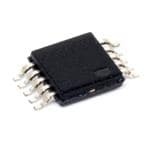
| 描述 | IC ADC 24BIT LP 10-MSOP模数转换器 - ADC 24-Bit SGL-Ch Ultra Low Power |
| 产品分类 | |
| 品牌 | Analog Devices |
| 产品手册 | |
| 产品图片 |
|
| rohs | 符合RoHS无铅 / 符合限制有害物质指令(RoHS)规范要求 |
| 产品系列 | 数据转换器IC,模数转换器 - ADC,Analog Devices AD7789BRMZ- |
| 数据手册 | |
| 产品型号 | AD7789BRMZ |
| 产品目录页面 | |
| 产品种类 | 模数转换器 - ADC |
| 位数 | 24 |
| 供应商器件封装 | 10-MSOP |
| 分辨率 | 24 bit |
| 包装 | 管件 |
| 商标 | Analog Devices |
| 安装类型 | 表面贴装 |
| 安装风格 | SMD/SMT |
| 封装 | Tube |
| 封装/外壳 | 10-TFSOP,10-MSOP(0.118",3.00mm 宽) |
| 封装/箱体 | MSOP-10 |
| 工作温度 | -40°C ~ 105°C |
| 工作电源电压 | 5 V |
| 工厂包装数量 | 50 |
| 接口类型 | Serial (3-Wire, SPI, QSPI, Microwire) |
| 数据接口 | DSP,MICROWIRE™,QSPI™,串行,SPI™ |
| 最大功率耗散 | 400 uW |
| 最大工作温度 | + 105 C |
| 最小工作温度 | - 40 C |
| 标准包装 | 50 |
| 特性 | - |
| 电压参考 | External |
| 电压源 | 单电源 |
| 系列 | AD7789 |
| 结构 | Sigma-Delta |
| 转换器数 | 1 |
| 转换器数量 | 1 |
| 转换速率 | 16.6 S/s |
| 输入数和类型 | 1 个差分,单极1 个差分,双极 |
| 输入类型 | Differential |
| 通道数量 | 1 Channel |
| 采样率(每秒) | - |


- 商务部:美国ITC正式对集成电路等产品启动337调查
- 曝三星4nm工艺存在良率问题 高通将骁龙8 Gen1或转产台积电
- 太阳诱电将投资9.5亿元在常州建新厂生产MLCC 预计2023年完工
- 英特尔发布欧洲新工厂建设计划 深化IDM 2.0 战略
- 台积电先进制程称霸业界 有大客户加持明年业绩稳了
- 达到5530亿美元!SIA预计今年全球半导体销售额将创下新高
- 英特尔拟将自动驾驶子公司Mobileye上市 估值或超500亿美元
- 三星加码芯片和SET,合并消费电子和移动部门,撤换高东真等 CEO
- 三星电子宣布重大人事变动 还合并消费电子和移动部门
- 海关总署:前11个月进口集成电路产品价值2.52万亿元 增长14.8%


PDF Datasheet 数据手册内容提取
Low Power, 16-/24-Bit, Sigma-Delta ADCs Data Sheet AD7788/AD7789 FEATURES FUNCTIONAL BLOCK DIAGRAM AD7788: 16-bit resolution REFIN(+) REFIN(–) GND VDD AD7789: 24-bit resolution AD7788/ Power AD7789 CLOCK Supply: 2.5 V to 5.25 V operation Normal: 75 µA maximum AIN(+) DOUT/RDY Power-down: 1 µA maximum AIN(–) AΣD-ΔC* INTSEEARRNFIDAALCE DSCINLK RMS noise: 1.5 µV CONTROL LOGIC CS AD7788: 16-bit p-p resolution AInDte7g7r8a9l :n 1o9n-blinite pa-rpit rye: s3o.5lu ptipomn (t2y1p.i5c abli ts effective) * AADD77778898:: 2146--BBIITT AADDCC 03539-001 Simultaneous 50 Hz and 60 Hz rejection Figure 1. Internal clock oscillator V monitor channel DD 10-lead MSOP INTERFACE 3-wire serial SPI-, QSPI™-, MICROWIRE-, and DSP-compatible Schmitt trigger on SCLK APPLICATIONS Smart transmitters Battery applications Portable instrumentation Sensor measurement Temperature measurement Pressure measurement Weigh scales 4 to 20 mA loops GENERAL DESCRIPTION The AD7788/AD7789 are low power, low noise, analog front The devices operate with a single power supply from 2.5 V to ends for low frequency measurement applications. The AD7789 5.25 V. When operating from a 3 V supply, the power dissipation contains a low noise, 24-bit, ∑-∆ analog-to-digital converter for the device is 225 µW maximum. The AD7788/AD7789 are (ADC) with one differential input. The AD7788 is a 16-bit available in a 10-lead MSOP. version of the AD7789. The devices operate from an internal clock. Therefore, the user does not have to supply a clock source to the devices. The output data rate is 16.6 Hz, which gives simultaneous 50 Hz/60 Hz rejection. Rev. C Document Feedback Information furnished by Analog Devices is believed to be accurate and reliable. However, no responsibility is assumed by Analog Devices for its use, nor for any infringements of patents or other One Technology Way, P.O. Box 9106, Norwood, MA 02062-9106, U.S.A. rights of third parties that may result from its use. Specifications subject to change without notice. No license is granted by implication or otherwise under any patent or patent rights of Analog Devices. Tel: 781.329.4700 ©2003–2016 Analog Devices, Inc. All rights reserved. Trademarks and registered trademarks are the property of their respective owners. Technical Support www.analog.com
AD7788/AD7789 Data Sheet TABLE OF CONTENTS Features .............................................................................................. 1 Communications Register ......................................................... 11 Interface ............................................................................................. 1 Status Register ............................................................................. 12 Applications ....................................................................................... 1 Mode Register ............................................................................. 13 Functional Block Diagram .............................................................. 1 Data Register ............................................................................... 13 General Description ......................................................................... 1 ADC Circuit Information .............................................................. 14 Revision History ............................................................................... 2 Noise Performance ..................................................................... 14 Specifications ..................................................................................... 3 Digital Interface .......................................................................... 14 AD7789 .......................................................................................... 3 Circuit Description......................................................................... 17 AD7788 .......................................................................................... 4 Analog Input Channel ............................................................... 17 AD7788/AD7789 .......................................................................... 5 Bipolar/Unipolar Configuration .............................................. 17 Timing Characteristics ................................................................ 6 Data Output Coding .................................................................. 17 Timing Diagrams .......................................................................... 7 Reference Input ........................................................................... 17 Absolute Maximum Ratings ............................................................ 8 V Monitor ................................................................................ 18 DD ESD Caution .................................................................................. 8 Grounding and Layout .............................................................. 18 Pin Configuration and Function Descriptions ............................. 9 Outline Dimensions ....................................................................... 19 Typical Performance Characteristics ........................................... 10 Ordering Guide .......................................................................... 19 On-Chip Registers .......................................................................... 11 REVISION HISTORY 4/16—Rev. B to Rev. C Change to (RS1, RS0 = 0, 1; Power-On/Reset = 0x02) Section ....... 13 Updated Outline Dimensions ....................................................... 19 Changes to Ordering Guide .......................................................... 19 3/06—Rev. A to Rev. B Changes to Ordering Guide .......................................................... 19 11/04—Rev. 0 to Rev. A Updated Format .................................................................. Universal Added Footnote 2 to Integral Nonlinearity A Grade ................... 4 Changes to Figure 5 .......................................................................... 9 Updated Outline Dimensions ....................................................... 19 Changes to Ordering Guide .......................................................... 19 8/03—Revision 0: Initial Version Rev. C | Page 2 of 20
Data Sheet AD7788/AD7789 SPECIFICATIONS AD7789 V = 2.5 V to 5.25 V; REFIN(+) = 2.5 V; REFIN(−) = GND; GND = 0 V; all specifications T to T , unless otherwise noted. DD MIN MAX Table 1. Parameter1 AD7789B Unit Test Conditions/Comments ADC CHANNEL SPECIFICATION Output Update Rate 16.6 Hz nom ADC CHANNEL No Missing Codes2 24 Bits min Resolution 19 Bits p-p Output Noise 1.5 µV rms typ Integral Nonlinearity ±15 ppm of FSR max Offset Error ±3 µV typ Offset Error Drift vs. Temperature ±10 nV/°C typ Full-Scale Error3 ±10 µV typ Gain Drift vs. Temperature ±0.5 ppm/°C typ Power Supply Rejection 90 dB min 100 dB typ, AIN = 1 V ANALOG INPUTS Differential Input Voltage Ranges ±REFIN V nom REFIN = REFIN(+) − REFIN(−) Absolute AIN Voltage Limits2 GND − 30 mV V min V + 30 mV V max DD Analog Input Current Input current varies with input voltage Average Input Current2 ±400 nA/V typ Average Input Current Drift ±50 pA/V/°C typ Normal-Mode Rejection2 At 50 Hz, 60 Hz 65 dB min 50 Hz ± 1 Hz, 60 Hz ± 1 Hz Common-Mode Rejection AIN = 1 V At DC 90 dB min 100 dB typ At 50 Hz, 60 Hz2 100 dB min 50 Hz ± 1 Hz, 60 Hz ± 1 Hz REFERENCE INPUT REFIN Voltage 2.5 V nom REFIN = REFIN(+) − REFIN(−) Reference Voltage Range2 0.1 V min V V max DD Absolute REFIN Voltage Limits2 GND − 30 mV V min V + 30 mV V max DD Average Reference Input Current 0.5 µA/V typ Average Reference Input Current Drift ±0.03 nA/V/°C typ Normal-Mode Rejection2 At 50 Hz, 60 Hz 65 dB min 50 Hz ± 1 Hz, 60 Hz ± 1 Hz Common-Mode Rejection AIN = 1 V At DC 110 dB typ At 50 Hz, 60 Hz 110 dB typ 50 Hz ± 1 Hz, 60 Hz ± 1 Hz 1 Temperature range: −40°C to +105°C. 2 Specification is not production tested but is supported by characterization data at initial product release. 3 Full-scale error applies to both positive and negative full scale and applies at the factory calibration conditions (VDD = 4 V). Rev. C | Page 3 of 20
AD7788/AD7789 Data Sheet AD7788 V = 2.5 V to 5.25 V (B grade); V = 2.7 V to 5.25 V (A grade); REFIN(+) = 2.5 V; REFIN(−) = GND; GND = 0 V; all specifications DD DD T to T , unless otherwise noted. MIN MAX Table 2. Parameter1 AD7788A, AD7788B Unit Test Conditions/Comments ADC CHANNEL SPECIFICATION Output Update Rate 16.6 Hz nom ADC CHANNEL No Missing Codes2 16 Bits min Resolution 16 Bits p-p Output Noise 1.5 µV rms typ Integral Nonlinearity ±15 ppm of FSR max B grade ±50 ppm of FSR max A grade2 Offset Error ±3 µV typ Offset Error Drift vs. Temperature ±10 nV/°C typ Full-Scale Error3 ±10 µV typ Gain Drift vs. Temperature ±0.5 ppm/°C typ Power Supply Rejection 90 dB min B grade 90 dB typ A grade ANALOG INPUTS Differential Input Voltage Ranges ±REFIN V nom REFIN = REFIN(+) − REFIN(−) Absolute AIN Voltage Limits2 GND − 30 mV V min V + 30 mV V max DD Analog Input Current Input current varies with input voltage Average Input Current2 ±400 nA/V typ Average Input Current Drift ±50 pA/V/°C typ Normal-Mode Rejection2 At 50 Hz, 60 Hz 65 dB min B grade, 50 Hz ± 1 Hz, 60 Hz ± 1 Hz 60 dB min A grade, 50 Hz ± 1 Hz, 60 Hz ± 1 Hz Common-Mode Rejection AIN = 1 V At DC 90 dB min B grade, 100 dB typ 90 dB typ A grade At 50 Hz, 60 Hz2 100 dB min B grade, 50 Hz ± 1 Hz, 60 Hz ± 1 Hz 100 dB typ A grade, 50 Hz ± 1 Hz, 60 Hz ± 1 Hz REFERENCE INPUT REFIN Voltage 2.5 V nom REFIN = REFIN(+) − REFIN(−) Reference Voltage Range2 0.1 V min V V max DD Absolute REFIN Voltage Limits2 GND − 30 mV V min V + 30 mV V max DD Average Reference Input Current 0.5 µA/V typ Average Reference Input Current Drift ±0.03 nA/V/°C typ Normal-Mode Rejection2 At 50 Hz, 60 Hz 65 dB min B grade, 50 Hz ± 1 Hz, 60 Hz ± 1 Hz 60 dB min A grade Common-Mode Rejection AIN = 1 V At DC 100 dB typ At 50 Hz, 60 Hz 110 dB typ 50 Hz ± 1 Hz, 60 Hz ± 1 Hz 1 Temperature range: B grade: −40°C to +105°C; A grade: −40°C to +85°C. 2 Specification is not production tested but is supported by characterization data at initial product release. 3 Full-scale error applies to both positive and negative full scale and applies at the factory calibration conditions (VDD = 4 V). Rev. C | Page 4 of 20
Data Sheet AD7788/AD7789 AD7788/AD7789 Table 3. Parameter AD7788A, AD7788B/AD7789B Unit Test Conditions/Comments LOGIC INPUTS All Inputs Except SCLK1 V , Input Low Voltage 0.8 V max V = 5 V INL DD 0.4 V max V = 3 V DD V , Input High Voltage 2.0 V min V = 3 V or 5 V INH DD SCLK Only (Schmitt-Triggered Input)1 V(+) 1.4/2 V min/V max V = 5 V T DD VT(−) 0.8/1.4 V min/V max VDD = 5 V VT(+) − VT(−) 0.3/0.85 V min/V max VDD = 5 V V(+) 0.9/2 V min/V max V = 3 V T DD VT(−) 0.4/1.1 V min/V max VDD = 3 V VT(+) − VT(−) 0.3/0.85 V min/V max VDD = 3 V Input Currents ±1 µA max V = V IN DD Input Capacitance 10 pF typ All digital inputs LOGIC OUTPUTS VOH, Output High Voltage1 VDD − 0.6 V min VDD = 3 V, ISOURCE = 100 µA V , Output Low Voltage1 0.4 V max V = 3 V, I = 100 µA OL DD SINK V , Output High Voltage1 4 V min V = 5 V, I = 200 µA OH DD SOURCE V , Output Low Voltage1 0.4 V max V = 5 V, I = 1.6 mA OL DD SINK Floating-State Leakage Current ±1 µA max Floating-State Output Capacitance 10 pF typ Data Output Coding Offset binary POWER REQUIREMENTS2 Power Supply Voltage VDD − GND 2.5/5.25 V min/max AD7789, AD7788 B grade 2.7/5.25 V min/max AD7788 A grade Power Supply Currents I Current 75 µA max 65 µA typ, V = 3.6 V DD DD 80 µA max 73 µA typ, V = 5.25 V DD I (Power-Down Mode) 1 µA max DD 1 Specification is not production tested but is supported by characterization data at initial product release. 2 Digital inputs equal to VDD or GND. Rev. C | Page 5 of 20
AD7788/AD7789 Data Sheet TIMING CHARACTERISTICS V = 2.5 V to 5.25 V (AD7788B and AD7789); V = 2.7 V to 5.25 V (AD7788A); GND = 0 V; REFIN(+) = 2.5 V; REFIN(−) = GND; DD DD Input Logic 0 = 0 V; Input Logic 1 = V , unless otherwise noted. DD Table 4. Parameter1, 2 Limit at T , T (B Version) Unit Description MIN MAX t 100 ns min SCLK high pulse width 3 t 100 ns min SCLK low pulse width 4 Read Operation t 0 ns min CS falling edge to DOUT/RDY active time 1 60 ns max V = 4.75 V to 5.25 V DD 80 ns max V = 2.7 V to 3.6 V DD t 3 0 ns min SCLK active edge to data valid delay4 2 60 ns max V = 4.75 V to 5.25 V DD 80 ns max V = 2.7 V to 3.6 V DD t 5, 6 10 ns min Bus relinquish time after CS inactive edge 5 80 ns max t 0 ns min SCLK inactive edge to CS inactive edge 6 t 10 ns min SCLK inactive edge to DOUT/RDY high 7 Write Operation t 0 ns min CS falling edge to SCLK active edge setup time4 8 t 30 ns min Data valid to SCLK edge setup time 9 t 25 ns min Data valid to SCLK edge hold time 10 t 0 ns min CS rising edge to SCLK edge hold time 11 1 Sample tested during initial release to ensure compliance. All input signals are specified with tR = tF = 5 ns (10% to 90% of VDD) and timed from a voltage level of 1.6 V. 2 See Figure 3 and Figure 4. 3 These numbers are measured with the load circuit of, and defined as, the time required for the output to cross the VOL or VOH limits. 4 SCLK active edge is the falling edge of SCLK. 5 These numbers are derived from the measured time taken by the data output to change 0.5 V when loaded with the circuit of Figure 2. The measured number is then extrapolated back to remove the effects of charging or discharging the 50 pF capacitor. This means that the times quoted in the Timing Characteristics are the true bus relinquish times of the device and, as such, are independent of external bus loading capacitances. 6 RDY returns high after a read of the ADC. In single-conversion mode and continuous-conversion mode, the same data can be read again, if required, while RDY is high, although care should be taken to ensure that subsequent reads do not occur close to the next output update. In continuous read mode, the digital word can be read only once. Rev. C | Page 6 of 20
Data Sheet AD7788/AD7789 TIMING DIAGRAMS ISINK (1.6mA WITH VDD = 5V, 100µA WITH VDD = 3V) TO OUTPUT 1.6V PIN 50pF I1S0O0UµRAC WE (IT20H0 VµADD W =I T3HV )VDD = 5V,03539-002 Figure 2. Load Circuit for Timing Characterization CS (I) t1 t6 t5 DOUT/RDY (O) MSB LSB t2 t7 t3 SCLK (I) I = INPUT, O = OUTPUT t4 03539-003 Figure 3. Read Cycle Timing Diagram CS (I) t8 t11 SCLK (I) t9 t10 DIN (I) MSB LSB I = INPUT, O = OUTPUT 03539-004 Figure 4. Write Cycle Timing Diagram Rev. C | Page 7 of 20
AD7788/AD7789 Data Sheet ABSOLUTE MAXIMUM RATINGS T = 25°C, unless otherwise noted. Stresses at or above those listed under Absolute Maximum A Ratings may cause permanent damage to the product. This is a Table 5. stress rating only; functional operation of the product at these Parameter Rating or any other conditions above those indicated in the operational V to GND −0.3 V to +7 V section of this specification is not implied. Operation beyond DD Analog Input Voltage to GND −0.3 V to V + 0.3 V the maximum operating conditions for extended periods may DD Reference Input Voltage to GND −0.3 V to V + 0.3 V affect product reliability. DD Total AIN/REFIN Current (Indefinite) 30 mA ESD CAUTION Digital Input Voltage to GND −0.3 V to V + 0.3 V DD Digital Output Voltage to GND −0.3 V to V + 0.3 V DD Operating Temperature Range B Grade −40°C to +105°C A Grade −40°C to +85°C Storage Temperature Range −65°C to +150°C Maximum Junction Temperature 150°C 10-Lead MSOP Thermal Impedance θ 206°C/W JA θ 44°C/W JC Lead Temperature, Soldering (10 sec) 300°C IR Reflow, Peak Temperature 220°C Rev. C | Page 8 of 20
Data Sheet AD7788/AD7789 PIN CONFIGURATION AND FUNCTION DESCRIPTIONS SCLK 1 AD7788/ 10 DIN CS 2 AD7789 9 DOUT/RDY AIN(+) 3 TOP VIEW 8 VDD REAFIINN((+–)) 45 (Not to Scale) 76 GRENFDIN(–) 03539-005 Figure 5. Pin Configuration Table 6. Pin Function Descriptions Pin No. Mnemonic Description 1 SCLK Serial Clock Input for Data Transfers to and from the ADC. The SCLK has a Schmitt-triggered input, making the interface suitable for opto-isolated applications. The serial clock can be continuous, with all data transmitted in a continuous train of pulses. Alternatively, it can be a noncontinuous clock with the information being trans- mitted to or from the ADC in smaller batches of data. 2 CS Chip Select Input. This is an active low logic input used to select the ADC. CS can be used to select the ADC in systems with more than one device on the serial bus or as a frame synchronization signal in communicating with the device. CS can be hardwired low, allowing the ADC to operate in 3-wire mode with SCLK, DIN, and DOUT/RDY used to interface with the device. 3 AIN(+) Analog Input. AIN(+) is the positive terminal of the fully differential analog input. 4 AIN(−) Analog Input. AIN(–) is the negative terminal of the fully differential analog input. 5 REFIN(+) Positive Reference Input. REFIN(+) can lie anywhere between V and GND + 0.1 V. The nominal reference DD voltage (REFIN(+) − REFIN(−)) is 2.5 V, but the device functions with a reference from 0.1 V to VDD. 6 REFIN(−) Negative Reference Input. This reference input can lie anywhere between GND and V − 0.1 V. DD 7 GND Ground Reference Point. 8 V Supply Voltage. 3 V or 5 V nominal. DD 9 DOUT/RDY The DOUT/RDY falling edge can be used as an interrupt to a processor, indicating that valid data is available. With an external serial clock, the data can be read using the DOUT/RDY pin. With CS low, the data/control word information is placed on the DOUT/RDY pin on the SCLK falling edge and is valid on the SCLK rising edge. The end of a conversion is also indicated by the RDY bit in the status register. When CS is high, the DOUT/RDY pin is three-stated, but the RDY bit remains active. 10 DIN Serial Data Input to the Input Shift Register on the ADC. Data in this shift register is transferred to the control registers within the ADC; the register selection bits of the communications register identify the appropriate register. Rev. C | Page 9 of 20
AD7788/AD7789 Data Sheet TYPICAL PERFORMANCE CHARACTERISTICS 0 8388625 –10 –20 –30 –40 –50 E dB–60 OD C –70 –80 –90 –100 ––112100 03539-007 8388591 VTAD D= =2 53°VC, ,V RRMEFS =N 2O.0IS4E8V =, 1.25µV 03539-009 0 20 40 60 80 100 120 140 160 0 200 400 600 800 1000 FREQUENCY (Hz) READ NO. Figure 6. Frequency Response with 16.6 Hz Update Rate Figure 8. AD7789 Noise Plot VDD = 3V 3.0 VDD = 5V 70 VREF = 2.048V UPDATE RATE = 16.6Hz TA = 25°C TA = 25°C RMS NOISE = 1.25µV 2.5 60 E50 V) 2.0 C µ REN40 SE ( OCCU30 S NOI 1.5 M R 1.0 20 0.5 100 03539-008 0 03539-013 8388591 8388625 0 0.5 1.0 1.5 2.0 2.5 3.0 3.5 4.0 4.5 5.0 CODE VREF (V) Figure 7. AD7789 Noise Histogram Figure 9. AD7788/AD7789 Noise vs. VREF Rev. C | Page 10 of 20
Data Sheet AD7788/AD7789 ON-CHIP REGISTERS The ADC is controlled and configured via a number of on-chip For read or write operations, once the subsequent read or write registers, which are described on the following pages. In the operation to the selected register is complete, the interface returns following descriptions, set implies a Logic 1 state and cleared to where it expects a write operation to the communications implies a Logic 0 state, unless otherwise stated. register. This is the default state of the interface and, on power-up or after a reset, the ADC is in this default state waiting for a write COMMUNICATIONS REGISTER operation to the communications register. In situations where the (RS1, RS0 = 0, 0) interface sequence is lost, a write operation of at least 32 serial The communications register is an 8-bit, write only register. All clock cycles with DIN high returns the ADC to this default state communications to the device must start with a write operation by resetting the entire device. Table 7 outlines the bit designations to the communications register. The data written to the commun- for the communications register. CR0 through CR7 indicate the ications register determines whether the next operation is a read bit location, CR denoting the bits are in the communications or write operation, and to which register this operation takes register. CR7 denotes the first bit of the data stream. The number in place. parentheses indicates the power-on/reset default status of that bit. CR7 CR6 CR5 CR4 CR3 CR2 CR1 CR0 WEN(0) 0(0) RS1(0) RS0(0) R/W(0) CREAD(0) CH1(0) CH0(0) Table 7. Communications Register Bit Designations Bit Location Bit Name Description CR7 WEN Write Enable Bit. A 0 must be written to this bit so that the write to the communications register actually occurs. If a 1 is the first bit written, the device does not clock on to subsequent bits in the register. It stays at this bit location until a 0 is written to this bit. Once a 0 is written to the WEN bit, the next seven bits are loaded to the communications register. CR6 0 This bit must be programmed with a Logic 0 for correct operation. CR5 to CR4 RS1 to RS0 Register Address Bits. These address bits are used to select which of the ADC registers are being selected during this serial interface communication (see Table 8). CR3 R/W A 0 in this bit location indicates that the next operation is a write to a specified register. A 1 in this position indicates that the next operation is a read from the designated register. CR2 CREAD Continuous Read of the Data Register. When this bit is set to 1 (and the data register is selected), the serial interface is configured so that the data register can be continuously read, that is, the contents of the data register are placed on the DOUT/RDY pin automatically when the SCLK pulses are applied. The communications register does not have to be written to for data reads. To enable continuous read mode, the instruction 001111XX must be written to the communications register. To exit the continuous read mode, the instruction 001110XX must be written to the communications register while the DOUT/RDY pin is low. While in continuous read mode, the ADC monitors activity on the DIN line so that it can receive the instruction to exit continuous read mode. Additionally, a reset occurs if 32 consecutive 1s are seen on DIN. Therefore, DIN should be held low in continuous read mode until an instruction is to be written to the device. CR1 to CR0 CH1 to CH0 These bits are used to select the analog input channel. The differential channel can be selected AIN(+)/AIN(−) or an internal short AIN(−)/AIN(−) can be selected. Alternatively, the power supply can be selected, that is, the ADC can measure the voltage on the power supply, which is useful for monitoring power supply variation. The power supply voltage is divided by 5 and then applied to the modulator for conversion. The ADC uses a 1.17 V ± 5% on-chip reference as the reference source for the analog-to-digital conversion. Any change in channel resets the filter and a new conversion is started. Rev. C | Page 11 of 20
AD7788/AD7789 Data Sheet Table 8. Register Selection RS1 RS0 Register Register Size 0 0 Communications register during a write operation 8-bit 0 0 Status register during a read operation 8-bit 0 1 Mode register 8-bit 1 0 Reserved 8-bit 1 1 Data register 16-bit (AD7788) 24-bit (AD7789) Table 9. Channel Selection CH1 CH0 Channel 0 0 AIN(+) − AIN(−) 0 1 Reserved 1 0 AIN(−) − AIN(−) 1 1 V monitor DD STATUS REGISTER (RS1, RS0 = 0, 0; Power-On/Reset = 0x88 for AD7788 and 0x8C for AD7789) The status register is an 8-bit, read only register. To access the ADC status register, the user must write to the communications register, select the next operation to be a read, and load Bit RS1 and Bit RS0 with 0. Table 10 outlines the bit designations for the status register. SR0 through SR7 indicate the bit locations, SR denoting the bits are in the status register. SR7 denotes the first bit of the data stream. The number(s) in parentheses indicates the power-on/reset default status of that bit. MSB LSB SR7 SR6 SR5 SR4 SR3 SR2 SR1 SR0 RDY(1) ERR(0) 0(0) 0(0) 1(1) WL(1/0) CH1(0) CH0(0) Table 10. Status Register Bit Designations Bit Location Bit Name Description SR7 RDY Ready Bit for ADC. Cleared when data is written to the ADC data register. The RDY bit is set automatically after the ADC data register has been read or a period of time before the data register is updated with a new conversion result to tell the user not to read the conversion data. It is also set when the device is placed in power-down mode. The end of a conversion is indicated by the DOUT/RDY pin. This pin can be used as an alternative to the status register for monitoring the ADC for conversion data. SR6 ERR ADC Error Bit. This bit is written to at the same time as the RDY bit. Set to indicate that the result written to the ADC data register has been clamped to all 0s or all 1s. Error sources include overrange, under- range. Cleared by a write operation to start a conversion. SR5 0 This bit is cleared automatically. SR4 0 This bit is cleared automatically. SR3 1 This bit is set automatically. SR2 WL AD7788/AD7789 Identifier. This bit is cleared automatically if the device is an AD7788 and it is set automatically if the device is an AD7789. This bit is used to distinguish between the AD7788 and AD7789. SR1 to SR0 CH1 to CH0 These bits indicate which channel is being converted by the ADC. Rev. C | Page 12 of 20
Data Sheet AD7788/AD7789 MODE REGISTER (RS1, RS0 = 0, 1; Power-On/Reset = 0x02) The mode register is an 8-bit register from which data can be read from or written to. This register is used to configure the ADC for range, to set unipolar or bipolar mode, or to place the device into power-down mode. Table 11 outlines the bit designations for the mode register. MR0 through MR7 indicate the bit locations, MR denoting the bits are in the mode register. MR7 denotes the first bit of the data stream. The number in parentheses indicates the power-on/reset default status of that bit. Any write to the setup register resets the modulator and filter, and sets the RDY bit. MSB LSB MR7 MR6 MR5 MR4 MR3 MR2 MR1 MR0 MD1(0) MD0(0) 0(0) 0(0) 0(0) U/B(0) 1(1) 0(0) Table 11. Mode Register Bit Designations Bit Location Bit Name Description MR7 to MR6 MD1 to MD0 Mode Select Bits. These bits select between continuous conversion mode, single conversion mode, and standby mode. In continuous conversion mode, the ADC continuously performs conversions and places the result in the data register. DOUT/ RDY goes low when a conversion is complete. The user can read these conversions by placing the device in continuous read mode whereby the conversions are automatically placed on the DOUT/ RDY line when SCLK pulses are applied. Alternatively, the user can instruct the ADC to output the conversion by writing to the communications register. After power-on, the first conversion is available after a period 2/ f while subsequent conversions are available at a frequency of f . In single ADC ADC conversion mode, the ADC is placed in power-down mode when conversions are not being performed. When single conversion mode is selected, the ADC powers up (which takes 1 ms) and performs a single conversion, requiring a duration of 2/f . The conversion result is placed in the data register, DOUT/ RDY ADC goes low, and the ADC returns to power-down mode. The conversion remains in the data register and DOUT/ RDY remains active (low) until the data is read or another conversion is performed (see Table 12). MR5 to MR3 0 These bits must be programmed with a Logic 0 for correct operation. MR2 U/B Unipolar/Bipolar Bit. Set by user to enable unipolar coding; that is, zero differential input results in 000…000 output, and a full-scale differential input results in 111…111 output. Cleared by the user to enable bipolar coding. Negative full-scale differential input results in an output code of 000…000, zero differential input results in an output code of 100…000, and a positive full-scale differential input results in an output code of 111…111. MR1 1 This bit must be programmed with a Logic 1 for correct operation. MR0 0 This bit must be programmed with a Logic 0 for correct operation. Table 12. Operating Modes MD1 MD0 Mode 0 0 Continuous conversion mode (default) 0 1 Reserved 1 0 Single conversion mode 1 1 Power-down mode DATA REGISTER (RS1, RS0 = 1, 1; Power-On/Reset = 0x0000 for the AD7788 and 0x000000 for the AD7789) The conversion result from the ADC is stored in this data register. This is a read only register. On completion of a read operation from this register, the RDY bit/pin is set. Rev. C | Page 13 of 20
AD7788/AD7789 Data Sheet ADC CIRCUIT INFORMATION The AD7788/AD7789 are low power ADCs that incorporate a operation or a write operation, and also determines to which Σ-Δ modulator and on-chip digital filtering intended for the register this read or write operation occurs. Therefore, write measurement of wide dynamic range, low frequency signals, access to any of the other registers on the devices begins with a such as those in pressure transducers, weigh scales, and temper- write operation to the communications register followed by a ature measurement applications. The device has one unbuffered write to the selected register. A read operation from any other differential input. The device requires an external reference register (except when continuous read mode is selected) starts voltage between 0.1 V and V . Figure 10 shows the basic with a write to the communications register followed by a read DD connections required to operate the device. operation from the selected register. POWER The AD7788/AD7789 serial interface consists of four signals: SUPPLY CS, DIN, SCLK, and DOUT/RDY. The DIN line is used to 0.1µF 10µF transfer data into the on-chip registers and DOUT/RDY is used for accessing data from the on-chip registers. SCLK is the serial VDD clock input for the device, and all data transfers (either on DIN REFIN(+) or DOUT/RDY ) occur with respect to the SCLK signal. The IN+ AD7788/ AD7789 DOUT/ RDY pin operates as a data ready signal also, the line OUT– OUT+ AIN(+) CS goes low when a new data-word is available in the output register. DOUT/RDY MICROCONTROLLER It is reset high when a read operation from the data register is IN– AIN(–) SCLK complete. It also goes high prior to the data register update to REFIN(–) indicate when not to read from the device; this ensures that a GND 03539-006 dCaSt ais r ueasedd i st on oset laetctte ma dpetevdic ew. hIti lcea tnh eb ere ugsiestde rt ois d beeciondge u tphde ated. Figure 10. Basic Connection Diagram AD7788/AD7789 in systems where several compo-nents are connected to the serial bus. The output rate of the AD7788/AD7789 (f ) is 16.6 Hz with ADC the settling time equal to 2 × t (120.4 ms). Normal-mode ADC Figure 3 and Figure 4 show timing diagrams for interfacing to rejection is the major function of the digital filter. Simultaneous the AD7788/AD7789 with CS being used to decode the devices. 50 Hz and 60 Hz rejection is optimized as notches are placed at Figure 3 shows the timing for a read operation from the output both 50 Hz and 60 Hz with this update rate (see Figure 6). shift register, while Figure 4 shows the timing for a write opera- NOISE PERFORMANCE tion to the input shift register. In all modes except continuous read mode, it is possible to read the same word from the data Typically, the devices have an rms noise of 1.5 μV rms that register several times even though the DOUT/RDY line returns corresponds to a peak-to-peak resolution of 16 bits for the high after the first read operation. However, care must be taken AD7788 and 19 bits (equivalent to an effective resolution of to ensure that the read operations have been completed before 21.5 bits) for the AD7789. These numbers are for the bipolar the next output update occurs. In continuous read mode, the input range with a reference of 2.5 V. The noise was measured data register can be read only once. with a differential input voltage of 0 V. The peak-to-peak resolution figures represent the resolution for which there is no The serial interface can operate in 3-wire mode by tying CS low. code flicker within a six-sigma limit. The output noise comes In this case, the SCLK, DIN, and DOUT/RDY lines are used to from two sources. The first is the electrical noise in the semi- communicate with the AD7788/AD7789. The end of conversion conductor devices (device noise) used in the implementation of can be monitored using the RDY bit in the status register. This the modulator. The second is quantization noise, added when scheme is suitable for interfacing to microcontrollers. If CS is the analog input is converted into the digital domain. required as a decoding signal, it can be generated from a port DIGITAL INTERFACE pin. For microcontroller interfaces, it is recommended that SCLK idles high between data transfers. As previously outlined, the AD7788/AD7789 programmable functions are controlled using a set of on-chip registers. Data is The AD7788/AD7789 can operate with CS being used as a written to these registers via the serial interface and read access frame synchronization signal. This scheme is useful for DSP to the on-chip registers is also provided by this interface. All interfaces. In this case, the first bit (MSB) is effectively clocked communications with the devices must start with a write to the out by CS, because CS normally occurs after the falling edge of communications register. After power-on or reset, the devices SCLK in DSPs. The SCLK can continue to run between data expect a write to the communications register. The data written transfers, provided the timing numbers are obeyed. to this register determines whether the next operation is a read Rev. C | Page 14 of 20
Data Sheet AD7788/AD7789 The serial interface can be reset by writing a series of 1s on the When the data-word has been read from the data register, DIN input. If a Logic 1 is written to the AD7788/AD7789 for at DOUT/RDY goes high. If CS is low, DOUT/RDY remains high least 32 serial clock cycles, the serial interface is reset. This until another conversion is initiated and completed. The data ensures that the interface can be reset to a known state if the register can be read several times, if required, even when interface gets lost due to a software error or a glitch in the system. DOUT/RDY has gone high. Reset returns the interface to the state in which it is expecting a Continuous Conversion Mode write to the communications register. This operation resets the contents of all registers to their power-on values. This is the default power-up mode. The AD7788/AD7789 continuously convert, the RDY pin in the status register going The AD7788/AD7789 can be configured to continuously low each time a conversion is complete. If CS is low, the convert or to perform a single conversion. See Figure 11 to DOUT/RDY line also goes low when a conversion is complete. Figure 13. To read a conversion, the user can write to the communications Single Conversion Mode register, indicating that the next operation is a read of the data In single-conversion mode, the AD7788/AD7789 are placed in register. The digital conversion is placed on the DOUT/RDY power-down mode between conversions. When a single conver- pin as soon as SCLK pulses are applied to the ADC. DOUT/ sion is initiated by setting MD1 to 1 and MD0 to 0 in the mode RDY returns high when the conversion is read. The user can register, the AD7788/AD7789 power up, perform a single con- read this register additional times, if required. However, the version, and then return to power-down mode. The devices user must ensure that the data register is not being accessed require 1 ms to power up and settle. The AD7788/AD7789 then at the completion of the next conversion or else the new perform a conversion, requiring a time period of 2 × tADC. conversion word is lost. DOUT/RDY goes low to indicate the completion of a conversion. CS DIN 0x10 0x82 0x38 DATA DOUT/RDY SCLK 03539-010 Figure 11. Single Conversion CS 0x38 0x38 DIN DATA DATA DOUT/RDY SCLK 03539-012 Figure 12. Continuous-Conversion Mode Rev. C | Page 15 of 20
AD7788/AD7789 Data Sheet Continuous Read Mode If the data-word has not read the conversion before the completion Rather than write to the communications register each time a of the next conversion, or if insufficient serial clocks are applied conversion is complete to access the data, the AD7788/AD7789 to the AD7788/AD7789 to read the word, the serial output can be placed in continuous read mode. By writing 001111XX register is reset when the next conversion is complete and the to the communications register, the user needs only to apply the new conversion is placed in the output serial register. appropriate number of SCLK cycles to the ADC and the data- To exit continuous read mode, the instruction 001110XX must word is automatically placed on the DOUT/RDY line when a be written to the communications register while the DOUT/ conversion is complete. RDY pin is low. While in continuous read mode, the ADC When DOUT/RDY goes low to indicate the end of a conver- monitors activity on the DIN line so that it can receive the instruction to exit continuous read mode. Additionally, a sion, sufficient SCLK cycles must be applied to the ADC and reset occurs if 32 consecutive 1s are seen on DIN. Therefore, the data conversion is placed on the DOUT/RDY line. When DIN should be held low in continuous read mode until an the conversion is read, DOUT/RDY returns high until the next instruction is to be written to the device. conversion is available. In this mode, the data can be read only once. Also, the user must ensure that the data-word is read before the next conversion is complete. CS 0x3C DIN DATA DATA DATA DOUT/RDY SCLK 03539-011 Figure 13. Continuous-Read Mode Rev. C | Page 16 of 20
Data Sheet AD7788/AD7789 CIRCUIT DESCRIPTION ANALOG INPUT CHANNEL DATA OUTPUT CODING The AD7788/AD7789 have one differential analog input channel When the ADC is configured for unipolar operation, the output that is connected to the modulator, thus, the input is unbuffered. code is natural (straight) binary with a zero differential input Note that this unbuffered input path provides a dynamic load to voltage resulting in a code of 000...000, a midscale voltage the driving source. Therefore, resistor/capacitor combinations on resulting in a code of 100...000, and a full-scale input voltage the input pins can cause dc gain errors, depending on the output resulting in a code of 111...111. The output code for any analog impedance of the source that is driving the ADC input. Table 13 input voltage can be represented as shows the allowable external resistance/capacitance values such that no gain error at the 16-bit level is introduced (AD7788). Code = 2N × (AIN/VREF) Table 14 shows the allowable external resistance/capacitance When the ADC is configured for bipolar operation, the output values such that no gain error at the 20-bit level is introduced code is offset binary with a negative full-scale voltage resulting (AD7789). in a code of 000...000, a zero differential input voltage resulting in a code of 100...000, and a positive full-scale input voltage Table 13. External R-C Combination for No 16-Bit Gain resulting in a code of 111...111. The output code for any analog Error (AD7788) input voltage can be represented as C (pF) R (Ω) 50 22.8 k Code = 2N – 1 × ((AIN/V ) + 1) REF 100 13.1 k 500 3.3 k where: 1000 1.8 k AIN is the analog input voltage. 5000 360 N = 16 for the AD7788, 24 for the AD7789. Table 14. External R-C Combination for No 20-Bit Gain REFERENCE INPUT Error (AD7789) The AD7788/AD7789 have a fully differential input capability C (pF) R (Ω) for the channel. The common-mode range for these differential 50 16.7 k inputs is from GND to V . The reference input is unbuffered 100 9.6 k DD and, therefore, excessive R-C source impedances introduce gain 500 2.2 k errors. The reference voltage REFIN (REFIN(+) − REFIN(−)) is 1000 1.1 k 2.5 V nominal, but the AD7788/AD7789 are functional with 5000 160 reference voltages from 0.1 V to V . In applications where the DD The absolute input voltage includes the range between GND − excitation (voltage or current) for the transducer on the analog 30 mV and V + 30 mV. The negative absolute input voltage input also drives the reference voltage for the devices, the effect DD limit does allow the possibility of monitoring small true bipolar of the low frequency noise in the excitation source is removed signals with respect to GND. because the application is ratiometric. If the AD7788/AD7789 are used in a nonratiometric application, a low noise reference BIPOLAR/UNIPOLAR CONFIGURATION should be used. The analog input to the devices can accept either unipolar or Recommended 2.5 V reference voltage sources for the AD7788/ bipolar input voltage ranges. A bipolar input range does not AD7789 include the ADR381 and ADR391, because they are imply that the devices can tolerate large negative voltages with low noise, low power references. If the analog circuitry uses a respect to system GND. Unipolar and bipolar signals on the 2.5 V power supply, the reference voltage source requires some AIN(+) input are referenced to the voltage on the AIN(−) input. headroom. In this case, a 2.048 V reference such as the ADR380 For example, if AIN(−) is 2.5 V and the ADC is configured for can be used. Again, these are low power, low noise references. unipolar mode, the input voltage range on the AIN(+) pin is Also note that the reference inputs provide a high impedance, 2.5 V to 5 V. If the ADC is configured for bipolar mode, the dynamic load. Because the input impedance of each reference analog input range on the AIN(+) input is 0 V to 5 V. The bipolar/ input is dynamic, resistor/capacitor combinations on these unipolar option is chosen by programming the U/B bit in the inputs can cause dc gain errors, depending on the output mode register. impedance of the source that is driving the reference inputs. Rev. C | Page 17 of 20
AD7788/AD7789 Data Sheet Reference voltage sources like those recommended in the pre- The printed circuit board that houses the AD7788/AD7789 vious section (for example, ADR391) typically have low output should be designed such that the analog and digital sections impedances and are, therefore, tolerant to having decoupling are separated and confined to certain areas of the board. A capacitors on REFIN(+) without introducing gain errors in the minimum etch technique is generally best for ground planes system. Deriving the reference input voltage across an external because it gives the best shielding. resistor means that the reference input sees a significant external It is recommended that the AD7788/AD7789 GND pins be tied source impedance. External decoupling on the REFIN pins is to the AGND plane of the system. In any layout, it is important not recommended in this type of circuit configuration. that the user consider the flow of currents in the system, ensuring VDD MONITOR that the return paths for all currents are as close as possible to the paths the currents took to reach their destinations. Avoid Along with converting external voltages, the analog input forcing digital currents to flow through the AGND sections of channel can be used to monitor the voltage on the V pin. DD the layout. When Bit CH1 and Bit CH0 in the communications register are set to 1, the voltage on the V pin is internally attenuated by 5 DD The AD7788/AD7789 ground plane should be allowed to run and the resultant voltage is applied to the Σ-Δ modulator using under the devices to prevent noise coupling. The power supply an internal 1.17 V reference for analog-to-digital conversion. lines to the AD7788/AD7789 should use as wide a trace as This is useful because variations in the power supply voltage possible to provide low impedance paths and reduce the effects can be monitored. of glitches on the power supply line. Fast switching signals, such GROUNDING AND LAYOUT as clocks, should be shielded with digital ground to avoid radiating noise to other sections of the board, and clock signals should Because the analog inputs and reference inputs of the ADC are never be run near the analog inputs. Avoid crossover of digital differential, most of the voltages in the analog modulator are and analog signals. Traces on opposite sides of the board should common-mode voltages. The excellent common-mode rejection run at right angles to each other. This reduces the effects of of the device removes common-mode noise on these inputs. feedthrough through the board. A microstrip technique is by far The digital filter provides rejection of broadband noise on the the best, but it is not always possible with a double-sided board. In power supply, except at integer multiples of the modulator this technique, the component side of the board is dedicated to sampling frequency. The digital filter also removes noise from ground planes, with signals placed on the solder side. the analog and reference inputs, provided that these noise sources do not saturate the analog modulator. As a result, the Good decoupling is important when using high resolution ADCs. AD7788/AD7789 are more immune to noise interference than V should be decoupled with a 10 µF tantalum in parallel with DD conventional high resolution converters. However, because the 0.1 µF capacitors to GND. To achieve the best from these resolution of the AD7788/AD7789 is so high, and the noise decoupling components, they should be placed as close as levels from the AD7788/AD7789 are so low, care must be taken possible to the device, ideally right up against the device. All with regard to grounding and layout. logic chips should be decoupled with 0.1 µF ceramic capacitors to DGND. Rev. C | Page 18 of 20
Data Sheet AD7788/AD7789 OUTLINE DIMENSIONS 3.10 3.00 2.90 10 6 5.15 3.10 4.90 3.00 4.65 2.90 1 5 PIN1 IDENTIFIER 0.50BSC 0.95 15°MAX 0.85 1.10MAX 0.75 0.70 0.15 0.30 6° 0.23 0.55 CO0P.0L5ANARITY 0.15 0° 0.13 0.40 0.10 COMPLIANTTOJEDECSTANDARDSMO-187-BA 091709-A Figure 14. 10-Lead Mini Small Outline Package [MSOP] (RM-10) Dimensions shown in millimeters ORDERING GUIDE Model1 Temperature Range Package Description Package Option Branding AD7788BRM −40°C to +105°C 10-Lead Mini Small Outline Package [MSOP] RM-10 COX AD7788BRMZ −40°C to +105°C 10-Lead Mini Small Outline Package [MSOP] RM-10 C3G AD7788BRMZ-REEL −40°C to +105°C 10-Lead Mini Small Outline Package [MSOP] RM-10 C3G AD7788ARM −40°C to +85°C 10-Lead Mini Small Outline Package [MSOP] RM-10 COZ AD7788ARMZ −40°C to +85°C 10-Lead Mini Small Outline Package [MSOP] RM-10 COZ AD7788ARMZ-REEL −40°C to +85°C 10-Lead Mini Small Outline Package [MSOP] RM-10 C4T AD7789BRM −40°C to +105°C 10-Lead Mini Small Outline Package [MSOP] RM-10 COY AD7789BRMZ −40°C to +105°C 10-Lead Mini Small Outline Package [MSOP] RM-10 C43 AD7789BRMZ-REEL −40°C to +105°C 10-Lead Mini Small Outline Package [MSOP] RM-10 C43 1 Z = RoHS Compliant Part. Rev. C | Page 19 of 20
AD7788/AD7789 Data Sheet NOTES ©2003–2016 Analog Devices, Inc. All rights reserved. Trademarks and registered trademarks are the property of their respective owners. D03539-0-4/16(C) Rev. C | Page 20 of 20
Mouser Electronics Authorized Distributor Click to View Pricing, Inventory, Delivery & Lifecycle Information: A nalog Devices Inc.: AD7788ARMZ AD7789BRM AD7788ARM AD7788BRM AD7788BRMZ AD7789BRMZ AD7789BRMZ-REEL AD7788BRMZ-REEL AD7788ARMZ-REEL