ICGOO在线商城 > 集成电路(IC) > 数据采集 - 模拟前端(AFE) > ADS131E04IPAGR

 Datasheet下载
- 型号: ADS131E04IPAGR
- 制造商: Texas Instruments
- 库位|库存: xxxx|xxxx
- 要求:
| 数量阶梯 | 香港交货 | 国内含税 |
| +xxxx | $xxxx | ¥xxxx |
查看当月历史价格
查看今年历史价格
ADS131E04IPAGR产品简介:
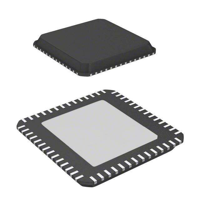
ICGOO电子元器件商城为您提供ADS131E04IPAGR由Texas Instruments设计生产,在icgoo商城现货销售,并且可以通过原厂、代理商等渠道进行代购。 ADS131E04IPAGR价格参考。Texas InstrumentsADS131E04IPAGR封装/规格:数据采集 - 模拟前端(AFE), 4 Channel AFE 16, 24 Bit 10.2mW 64-TQFP (10x10)。您可以下载ADS131E04IPAGR参考资料、Datasheet数据手册功能说明书,资料中有ADS131E04IPAGR 详细功能的应用电路图电压和使用方法及教程。
Texas Instruments(德州仪器)的ADS131E04IPAGR是一款高性能、低功耗的24位模数转换器(ADC),属于数据采集系统中的模拟前端(AFE)产品。其应用场景主要包括以下几个方面:

 1. 医疗设备
   - 心电图(ECG/EKG)监测:ADS131E04IPAGR具有高分辨率和低噪声特性,非常适合用于心电图设备中,能够精确采集心脏电信号。
   - 生物电势测量:可用于脑电图(EEG)、肌电图(EMG)等生物信号采集,支持多通道同步采样,满足高精度需求。

 2. 工业自动化
   - 传感器信号调理:适用于压力、温度、振动等传感器信号的高精度采集,广泛用于工业控制和监测系统。
   - 过程控制:在工厂自动化中,该器件可用于实时监测和控制关键参数,确保系统的稳定性和可靠性。

 3. 能源管理
   - 智能电网监控:用于电力线路电流和电压信号的高精度采集,支持电网状态的实时分析。
   - 电池管理系统(BMS):能够精确测量电池组的电压、电流和温度,提升电池的安全性和寿命。

 4. 环境监测
   - 气象站:用于采集风速、湿度、气压等环境参数,提供高精度的数据支持。
   - 水质检测:对水体中的电导率、pH值等参数进行精确测量。

 5. 科研与测试设备
   - 实验室仪器:如示波器、信号分析仪等,需要高精度数据采集的场景。
   - 振动与噪声分析:用于机械设备的故障诊断和性能优化。

 核心优势
- 24位分辨率:提供极高的测量精度。
- 低功耗设计:适合便携式和电池供电设备。
- 多通道同步采样:支持复杂系统的多点数据采集。
- 内置PGA(可编程增益放大器):简化信号调理电路设计。

综上,ADS131E04IPAGR凭借其高精度、低功耗和灵活性,广泛应用于医疗、工业、能源、环境监测及科研等领域,是高性能数据采集系统的核心组件之一。
| 参数 | 数值 |
| 产品目录 | 集成电路 (IC) |
| 描述 | IC AFE 16/24BIT 64KSPS 64TQFP |
| 产品分类 | 数据采集 - 模拟前端 (AFE) |
| 品牌 | Texas Instruments |
| 数据手册 | |
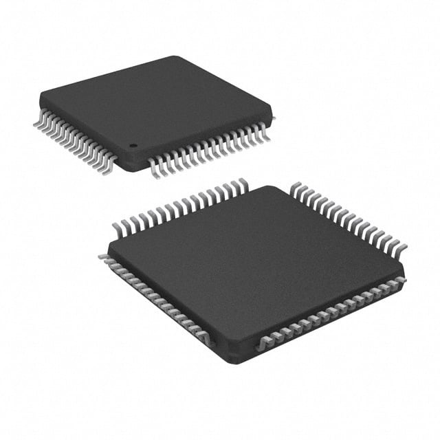
| 产品图片 |
|
| 产品型号 | ADS131E04IPAGR |
| rohs | 无铅 / 符合限制有害物质指令(RoHS)规范要求 |
| 产品系列 | - |
| 位数 | 16,24 |
| 供应商器件封装 | 64-TQFP(10x10) |
| 其它名称 | ADS131E04IPAGR-ND |
| 功率(W) | 10.2mW |
| 包装 | 带卷 (TR) |
| 封装/外壳 | 64-TQFP |
| 标准包装 | 1,500 |
| 电压-电源,数字 | 1.8 V ~ 3.6 V |
| 电压-电源,模拟 | 2.7 V ~ 5.25 V |
| 通道数 | 4 |


PDF Datasheet 数据手册内容提取
Product Order Technical Tools & Support & Folder Now Documents Software Community ADS131E04,ADS131E06,ADS131E08 SBAS561C–JUNE2012–REVISEDJANUARY2017 ADS131E0x 4-, 6-, and 8-Channel, 24-Bit, Simultaneously-Sampling, Delta-Sigma ADC 1 Features The ADS131E0x have a flexible input multiplexer per channel that can be independently connected to the • EightDifferentialADCInputs 1 internally-generated signals for test, temperature, and • OutstandingPerformance: fault detection. Fault detection can be implemented – DynamicRange:118dBat1kSPS internal to the device, using the integrated comparators with digital-to-analog converter (DAC)- – Crosstalk: –110dB controlledtriggerlevels.TheADS131E0xcanoperate – THD:–90dBat50Hzand60Hz atdataratesashighas64kSPS. • AnalogSupplyRangeOptions: These complete analog front-end (AFE) solutions are – 3Vto5V(Unipolar) packaged in a TQFP-64 package and are specified – ±2.5V(Bipolar,AllowsDC-Coupling) over the industrial temperature range of –40°C to +105°C. • Digital:1.8Vto3.6V • LowPower:2mWperChannel DeviceInformation(1) • DataRates:1,2,4,8,16,32,and64kSPS PARTNUMBER PACKAGE BODYSIZE(NOM) • ProgrammableGains:1,2,4,8,and12 ADS131E0x TQFP(64) 10.00mm×10.00mm • FaultDetectionandDeviceTestingCapability (1) For all available packages, see the orderable addendum at • SPI™DataInterfaceandFourGPIOs theendofthedatasheet. • Package:TQFP-64(PAG) ADS131E08SimplifiedSchematic • OperatingTemperatureRange: –40°Cto+105°C Current Line A Sensing Channel 1 PGA AßD(cid:8)C Device 2 Applications SVeonltsaigneg Channel 2 PGA AßD(cid:8)C Voltage • PowerProtection:CircuitBreakers,andRelay Reference Protection SCeunrrseinngt Channel 3 PGA AßD(cid:8)C Oscillator • EnergyMetering:SinglePhase,Polyphase,and Line B PowerQuality SVeonltsaigneg EMI Channel 4 PGA AßD(cid:8)C Filters Control • BatteryTestSystems and and Input SPI Interface • TestandMeasurement SCeunrrseinngt MUX Channel 5 PGA AßD(cid:8)C Line C • SimultaneousSamplingDataAcquisitionSystems SVeonltsaigneg Channel 6 PGA AßD(cid:8)C DeFteacutliton 3 Description Current Channel 7 PGA AßD(cid:8)C Test The ADS131E0x are a family of multichannel, Sensing Line N simultaneous sampling, 24-bit, delta-sigma (ΔΣ), Voltage Channel 8 PGA AßD(cid:8)C AOmpp analog-to-digital converters (ADCs) with a built-in Sensing programmable gain amplifier (PGA), internal reference, and an onboard oscillator. The ADC wide dynamic range, scalable data rates, and internal fault detect monitors make the ADS131E0x attractive in industrial power monitoring and protection as well as test and measurement applications. True high- impedance inputs enable the ADS131E0x to directly interface with a resistor-divider network or a voltage transformer to measure line voltage, or a current transformer or Rogowski coil to measure line current. With high integration levels and exceptional performance, the ADS131E0x family enables the creation of scalable industrial power systems at significantly reduced size, power, and low overall cost. 1 An IMPORTANT NOTICE at the end of this data sheet addresses availability, warranty, changes, use in safety-critical applications, intellectualpropertymattersandotherimportantdisclaimers.PRODUCTIONDATA.
ADS131E04,ADS131E06,ADS131E08 SBAS561C–JUNE2012–REVISEDJANUARY2017 www.ti.com Table of Contents 1 Features.................................................................. 1 9.5 Programming...........................................................33 2 Applications........................................................... 1 9.6 RegisterMap...........................................................39 3 Description............................................................. 1 10 ApplicationandImplementation........................ 49 4 RevisionHistory..................................................... 2 10.1 ApplicationInformation..........................................49 10.2 TypicalApplication................................................58 5 DeviceComparison............................................... 4 11 PowerSupplyRecommendations..................... 61 6 PinConfigurationandFunctions......................... 4 11.1 Power-UpTiming..................................................61 7 Specifications......................................................... 7 11.2 RecommendedExternalCapacitorValues...........62 7.1 AbsoluteMaximumRatings......................................7 11.3 DeviceConnectionsforUnipolarPowerSupplies 62 7.2 ESDRatings..............................................................7 11.4 DeviceConnectionsforBipolarPowerSupplies..63 7.3 RecommendedOperatingConditions.......................7 12 Layout................................................................... 64 7.4 ThermalInformation..................................................8 12.1 LayoutGuidelines.................................................64 7.5 ElectricalCharacteristics...........................................9 12.2 LayoutExample....................................................64 7.6 TimingRequirements..............................................12 13 DeviceandDocumentationSupport................. 66 7.7 SwitchingCharacteristics........................................12 7.8 TypicalCharacteristics............................................13 13.1 DeviceSupport......................................................66 13.2 RelatedLinks........................................................66 8 ParameterMeasurementInformation................16 13.3 ReceivingNotificationofDocumentationUpdates66 8.1 NoiseMeasurements..............................................16 13.4 CommunityResource............................................66 9 DetailedDescription............................................ 17 13.5 Trademarks...........................................................66 9.1 Overview.................................................................17 13.6 ElectrostaticDischargeCaution............................66 9.2 FunctionalBlockDiagram.......................................18 13.7 Glossary................................................................66 9.3 FeatureDescription................................................19 14 Mechanical,Packaging,andOrderable 9.4 DeviceFunctionalModes........................................28 Information........................................................... 67 4 Revision History NOTE:Pagenumbersforpreviousrevisionsmaydifferfrompagenumbersinthecurrentversion. ChangesfromRevisionB(December2013)toRevisionC Page • AddedESDRatingstable,FeatureDescriptionsection,DeviceFunctionalModes,ApplicationandImplementation section,PowerSupplyRecommendationssection,Layoutsection,DeviceandDocumentationSupportsection,and Mechanical,Packaging,andOrderableInformationsection ................................................................................................. 1 • ChangedformattingofThermalInformationtablenote ......................................................................................................... 8 ChangesfromRevisionA(April2013)toRevisionB Page • Deleteddevicegraphic........................................................................................................................................................... 1 • ChangedADS131E0xfamilydescriptionto24-bitsonlythroughoutdocument..................................................................... 1 • AddedAVSStoDGNDrowtoAbsoluteMaximumRatingstable.......................................................................................... 7 • ChangedminimumspecificationtoExternalReference,VREFPparameterinElectricalCharacteristicstable....................7 • ChangedconditionsinFigure10.......................................................................................................................................... 13 • ChangedconditionsinFigure11.......................................................................................................................................... 13 • ChangedSTARTOpcodetoSTARTinFigure39................................................................................................................ 28 • ChangedReset(RESET)sectionforclarity......................................................................................................................... 29 • ChangedPower-UpSequencingsection.............................................................................................................................. 61 ChangesfromOriginal(June2012)toRevisionA Page • DeletedAGNDtoDGNDrowfromAbsoluteMaximumRatingstable................................................................................... 7 • ChangedvalueofDigitalinputtoDVDDrowinAbsoluteMaximumRatingstable................................................................ 7 • AddedminimumandmaximumspecificationstoExternalReference,ReferenceinputvoltageparameterinElectrical 2 SubmitDocumentationFeedback Copyright©2012–2017,TexasInstrumentsIncorporated ProductFolderLinks:ADS131E04 ADS131E06 ADS131E08
ADS131E04,ADS131E06,ADS131E08 www.ti.com SBAS561C–JUNE2012–REVISEDJANUARY2017 Characteristicstable............................................................................................................................................................... 7 • AddedminimumandmaximumspecificationstoExternalReference,VREFPparameterinElectricalCharacteristics table........................................................................................................................................................................................ 7 • ChangedChannelPerformance(ACPerformance),AccuracyparameterinElectricalCharacteristicstable.......................9 • ChangedInternalReference,V parameterinElectricalCharacteristicstable..................................................................... 9 O • ChangedInternalReference,TemperaturedriftparameterinElectricalCharacteristicstable.............................................. 9 • AddedFigure15 .................................................................................................................................................................. 14 Copyright©2012–2017,TexasInstrumentsIncorporated SubmitDocumentationFeedback 3 ProductFolderLinks:ADS131E04 ADS131E06 ADS131E08
ADS131E04,ADS131E06,ADS131E08 SBAS561C–JUNE2012–REVISEDJANUARY2017 www.ti.com 5 Device Comparison PRODUCT NO.OFINPUTS REFERENCEOPTIONS RESOLUTION(Bits) POWER-UPTIME(ms) ADS130E08 8 Internal,external 16 128 ADS131E04 4 Internal,external 24 128 ADS131E06 6 Internal,external 24 128 ADS131E08 8 Internal,external 24 128 ADS131E08S 8 Internalonly 24 3 6 Pin Configuration and Functions PAGPackage 64-PinTQFP TopView T U AMPO AMPN AMPP DD SS SS DD AP3 DD1 SS1 KSEL ND DD ND C P C P P V V V V C V V L G V G N O N O O A A A A V A A C D D D 4 3 2 1 0 9 8 7 6 5 4 3 2 1 0 9 6 6 6 6 6 5 5 5 5 5 5 5 5 5 5 4 IN8N 1 48 DVDD IN8P 2 47 DRDY IN7N 3 46 GPIO4 IN7P 4 45 GPIO3 IN6N 5 44 GPIO2 IN6P 6 43 DOUT IN5N 7 42 GPIO1 IN5P 8 41 DAISY_IN IN4N 9 40 SCLK IN4P 10 39 CS IN3N 11 38 START IN3P 12 37 CLK IN2N 13 36 RESET IN2P 14 35 PWDN IN1N 15 34 DIN IN1P 16 33 DGND 7 8 9 0 1 2 3 4 5 6 7 8 9 0 1 2 1 1 1 2 2 2 2 2 2 2 2 2 2 3 3 3 P N D S D D S P N 4 C 1 C 2 1 S Not to scale T T D S D D S F F P N P N P V S S S V V V V V E E A A A S V E E A A A A A R R C C C E A T T V V V V V R 4 SubmitDocumentationFeedback Copyright©2012–2017,TexasInstrumentsIncorporated ProductFolderLinks:ADS131E04 ADS131E06 ADS131E08
ADS131E04,ADS131E06,ADS131E08 www.ti.com SBAS561C–JUNE2012–REVISEDJANUARY2017 PinFunctions PIN I/O DESCRIPTION NAME NO. Analogsupply.Connecta1-µF(orlarger)capacitortoAVSSforeach AVDD 19,21,22,56,59 Supply AVDDpin. Chargepumpanalogsupply.Connecta1-µF(orlarger)capacitorto AVDD1 54 Supply AVSS1. AVSS 20,23,32,57,58 Supply Analogground AVSS1 53 Supply Chargepumpanalogground CS 39 Digitalinput Chipselect;activelow CLK 37 Digitalinput Masterclockinput.ConnecttoDGNDifunused. CLKSEL 52 Digitalinput Masterclockselect DAISY_IN 41 Digitalinput Daisy-chaininput.ConnecttoDGNDifunused. DGND 33,49,51 Supply Digitalground DIN 34 Digitalinput Serialdatainput DOUT 43 Digitaloutput Serialdataoutput Dataready;activelow.ConnecttoDGNDwitha10-kΩresistorif DRDY 47 Digitaloutput unused. Digitalcorepowersupply.Connecta1-µF(orlarger)capacitorto DVDD 48,50 Supply DGNDforeachDVDDpin. General-purposeinput/outputpin1.ConnecttoDGNDwitha10-kΩ GPIO1 42 Digitalinput/output resistorifunused. General-purposeinput/outputpin2.ConnecttoDGNDwitha10-kΩ GPIO2 44 Digitalinput/output resistorifunused. General-purposeinput/outputpin3.ConnecttoDGNDwitha10-kΩ GPIO3 45 Digitalinput/output resistorifunused. General-purposeinput/outputpin4.ConnecttoDGNDwitha10-kΩ GPIO4 46 Digitalinput/output resistorifunused. IN1N(1) 15 Analoginput Negativeanaloginput1 IN1P(1) 16 Analoginput Positiveanaloginput1 IN2N(1) 13 Analoginput Negativeanaloginput2 IN2P(1) 14 Analoginput Positiveanaloginput2 IN3N(1) 11 Analoginput Negativeanaloginput3 IN3P(1) 12 Analoginput Positiveanaloginput3 IN4N(1) 9 Analoginput Negativeanaloginput4 IN4P(1) 10 Analoginput Positiveanaloginput4 IN5N(1) 7 Analoginput Negativeanaloginput5(ADS131E06andADS131E08only) IN5P(1) 8 Analoginput Positiveanaloginput5(ADS131E06andADS131E08only) IN6N(1) 5 Analoginput Negativeanaloginput6(ADS131E06andADS131E08only) IN6P(1) 6 Analoginput Positiveanaloginput6(ADS131E06andADS131E08only) IN7N(1) 3 Analoginput Negativeanaloginput7(ADS131E08only) IN7P(1) 4 Analoginput Positiveanaloginput7(ADS131E08only) IN8N(1) 1 Analoginput Negativeanaloginput8(ADS131E08only) IN8P(1) 2 Analoginput Positiveanaloginput8(ADS131E08only) Noconnection,leavefloating.CanbeconnectedtoAVDDorAVSS NC 27,29,62,64 — witha10-kΩorhigherresistor. Opampinvertinginput;leavefloatingifunusedandpower-downthe OPAMPN 61 Analoginput opamp. Opampnoninvertinginput;leavefloatingifunusedandpower-down OPAMPP 60 Analoginput theopamp. OPAMPOUT 63 Analogoutput Opampoutput;leavefloatingifunusedandpower-downtheopamp. PWDN 35 Digitalinput Power-down;activelow (1) Connectanyunusedorpowered-downanaloginputpinstoAVDD. Copyright©2012–2017,TexasInstrumentsIncorporated SubmitDocumentationFeedback 5 ProductFolderLinks:ADS131E04 ADS131E06 ADS131E08
ADS131E04,ADS131E06,ADS131E08 SBAS561C–JUNE2012–REVISEDJANUARY2017 www.ti.com PinFunctions(continued) PIN I/O DESCRIPTION NAME NO. RESET 36 Digitalinput Systemreset;activelow RESV1 31 Digitalinput Reservedforfutureuse.ConnectdirectlytoDGND. SCLK 40 Digitalinput Serialclockinput START 38 Digitalinput Startconversion Testsignal,negativepin.SeetheUnusedInputsandOutputssection TESTN 18 Analoginput/output forunusedpins. Testsignal,positivepin.SeetheUnusedInputsandOutputssection TESTP 17 Analoginput/output forunusedpins. VCAP1 28 Analogoutput Analogbypasscapacitor.Connecta22-µFcapacitortoAVSS. VCAP2 30 Analogoutput Analogbypasscapacitor.Connecta1-µFcapacitortoAVSS. Analogbypasscapacitor.Connectaparallelcombinationof1-µFand VCAP3 55 Analogoutput 0.1-µFcapacitorstoAVSS. VCAP4 26 Analogoutput Analogbypasscapacitor.Connecta1-µFcapacitortoAVSS. VREFN 25 Analoginput Negativereferencevoltage.ConnecttoAVSS Positivereferencevoltage.Connectaminimum10-µFcapacitorto VREFP 24 Analoginput/output VREFN. 6 SubmitDocumentationFeedback Copyright©2012–2017,TexasInstrumentsIncorporated ProductFolderLinks:ADS131E04 ADS131E06 ADS131E08
ADS131E04,ADS131E06,ADS131E08 www.ti.com SBAS561C–JUNE2012–REVISEDJANUARY2017 7 Specifications 7.1 Absolute Maximum Ratings overoperatingfree-airtemperaturerange(unlessotherwisenoted)(1) MIN MAX UNIT AVDDtoAVSS –0.3 5.5 Power-supplyvoltage AVSStoDGND –3 0.2 V DVDDtoDGND –0.3 3.9 Analoginputvoltage AnaloginputtoAVSS AVSS–0.3 AVDD+0.3 V Digitalinputvoltage DigitalinputtoDVDD DGND–0.3 DVDD+0.3 V Momentary –100 100 Inputcurrent mA Continuous,allotherpinsexceptpower-supplypins –10 10 Junction,T 150 J Temperature °C Storage,T –60 150 stg (1) StressesbeyondthoselistedunderAbsoluteMaximumRatingsmaycausepermanentdamagetothedevice.Thesearestressratings only,whichdonotimplyfunctionaloperationofthedeviceattheseoranyotherconditionsbeyondthoseindicatedunderRecommended OperatingConditions.Exposuretoabsolute-maximum-ratedconditionsforextendedperiodsmayaffectdevicereliability. 7.2 ESD Ratings VALUE UNIT Human-bodymodel(HBM),perANSI/ESDA/JEDECJS-001(1) ±1000 V(ESD) Electrostaticdischarge Charged-devicemodel(CDM),perJEDECspecificationJESD22- V C101(2) ±500 (1) JEDECdocumentJEP155statesthat500-VHBMallowssafemanufacturingwithastandardESDcontrolprocess. (2) JEDECdocumentJEP157statesthat250-VCDMallowssafemanufacturingwithastandardESDcontrolprocess. 7.3 Recommended Operating Conditions overoperatingfree-airtemperaturerange(unlessotherwisenoted) MIN NOM MAX UNIT POWERSUPPLY AVDD Analogpowersupply AVDDtoAVSS 2.7 5.0 5.25 V DVDD Digitalpowersupply DVDDtoDGND 1.7 1.8 3.6 V Analogtodigitalsupply AVDDtoDVDD –2.1 3.6 V ANALOGINPUTS VIN Differentialinputvoltage VIN=V(INxP)–V(INxN) –VREF/Gain VREF/Gain V VCM Common-modeinputvoltage VCM=(V(INxP)–V(INxN))/2 SeetheInputCommon-ModeRangesection V VOLTAGEREFERENCEINPUTS AVDD=3V,VREF=(VVREFP– 2 2.5 AVDD V VVREFN) VREF Referenceinputvoltage AVDD=5V,VREF=(VVREFP– 2 4 AVDD V VVREFN) VREFN Negativereferenceinput AVSS V VREFP Positiveinput AVDD–3 AVSS+2.5 AVDD V EXTERNALCLOCKSOURCE CLKSELpin=0, 1.7 2.048 2.25 (AVDD–AVSS)=3V fCLK Masterclockrate MHz CLKSELpin=0, 1.0 2.048 2.25 (AVDD–AVSS)=5V DIGITALINPUTS Inputvoltage DGND–0.1 DVDD+0.1 V TEMPERATURERANGE TA Operatingambienttemperature –40 105 °C Copyright©2012–2017,TexasInstrumentsIncorporated SubmitDocumentationFeedback 7 ProductFolderLinks:ADS131E04 ADS131E06 ADS131E08
ADS131E04,ADS131E06,ADS131E08 SBAS561C–JUNE2012–REVISEDJANUARY2017 www.ti.com 7.4 Thermal Information ADS131E0x THERMALMETRIC(1) PAG(TQFP) UNIT 64PINS R Junction-to-ambientthermalresistance 35 °C/W θJA R Junction-to-case(top)thermalresistance 31 °C/W θJC(top) R Junction-to-boardthermalresistance 26 °C/W θJB ψ Junction-to-topcharacterizationparameter 0.1 °C/W JT ψ Junction-to-boardcharacterizationparameter NA °C/W JB R Junction-to-case(bottom)thermalresistance NA °C/W θJC(bot) (1) Formoreinformationabouttraditionalandnewthermalmetrics,seetheSemiconductorandICPackageThermalMetricsapplication report. 8 SubmitDocumentationFeedback Copyright©2012–2017,TexasInstrumentsIncorporated ProductFolderLinks:ADS131E04 ADS131E06 ADS131E08
ADS131E04,ADS131E06,ADS131E08 www.ti.com SBAS561C–JUNE2012–REVISEDJANUARY2017 7.5 Electrical Characteristics Minimumandmaximumspecificationsapplyfrom–40°Cto+105°C.Typicalspecificationsareat25°C.Allspecificationsare atDVDD=1.8V,AVDD=3V,AVSS=0V,V =2.4V,externalf =2.048MHz,datarate=8kSPS,andgain=1, REF CLK unlessotherwisenoted. PARAMETER TESTCONDITIONS MIN TYP MAX UNIT ANALOGINPUTS Ci Inputcapacitance 20 pF IIB Inputbiascurrent PGAoutputinnormalrange 5 nA DCinputimpedance 200 MΩ PGAPERFORMANCE Gainsettings 1,2,4,8,12 BW Bandwidth SeeTable3 ADCPERFORMANCE DR Datarate fCLK=2.048MHz 1 64 kSPS DR=1kSPS,2kSPS,4kSPS,8kSPS,and16kSPS 24 Bits Resolution DR=32kSPSand64kSPS 16 Bits CHANNELPERFORMANCE(DCPERFORMANCE) INL Integralnonlinearity Full-scale,bestfit 10 ppm G=1 105 dB Dynamicrange SeetheNoiseMeasurements Gainsettingsotherthan1 section EO Offseterror 350 μV Offseterrordrift 0.65 μV/°C EG Gainerror Excludingvoltagereferenceerror 0.1% Gaindrift Excludingvoltagereferencedrift 3 ppm/°C Gainmatchbetweenchannels 0.2 %ofFS CHANNELPERFORMANCE(ACPERFORMANCE) CMRR Common-moderejectionratio fCM=50Hzand60Hz(1) –110 dB PSRR Power-supplyrejectionratio fPS=50Hzand60Hz –80 dB Crosstalk fIN=50Hzand60Hz –110 dB 3000:1dynamicrangewitha1- AVDD=3V,VREF=2.4V 0.04% Accuracy secondmeasurement (VRMS/IRMS) AVDD=5V,VREF=4V 0.025% SNR Signal-to-noiseratio fIN=50Hzand60Hz,gain=1 107 dB THD Totalharmonicdistortion 10Hz,–0.5dBFs –93 dB INTERNALREFERENCE TA=25°C,VREF=2.4V 2.394 2.4 2.406 V VREF Outputvoltage TA=25°C,VREF=4V 4 V VREFaccuracy ±0.2% Temperaturedrift TA=–40°Cto+105°C 20 ppm/°C Start-uptime Settledto0.2% 150 ms EXTERNALREFERENCE Inputimpedance 6 kΩ INTERNALOSCILLATOR ±2% Accuracy TA=25°C ±0.5% TA=–40°Cto105°C 2.5% Internaloscillatorclockfrequency Nominalfrequency 2.048 MHz Internaloscillatorstart-uptime 20 μs Internaloscillatorpower 120 μW consumption FAULTDETECTANDALARM Comparatorthresholdaccuracy ±30 mV (1) CMRRismeasuredwithacommon-modesignalof(AVSS+0.3V)to(AVDD–0.3V).Thevaluesindicatedaretheminimumofthe eightchannels. Copyright©2012–2017,TexasInstrumentsIncorporated SubmitDocumentationFeedback 9 ProductFolderLinks:ADS131E04 ADS131E06 ADS131E08
ADS131E04,ADS131E06,ADS131E08 SBAS561C–JUNE2012–REVISEDJANUARY2017 www.ti.com Electrical Characteristics (continued) Minimumandmaximumspecificationsapplyfrom–40°Cto+105°C.Typicalspecificationsareat25°C.Allspecificationsare atDVDD=1.8V,AVDD=3V,AVSS=0V,V =2.4V,externalf =2.048MHz,datarate=8kSPS,andgain=1, REF CLK unlessotherwisenoted. PARAMETER TESTCONDITIONS MIN TYP MAX UNIT OPERATIONALAMPLIFIER Integratednoise 0.1Hzto250Hz 9 µVRMS Noisedensity 2kHz 120 nV/√Hz GBP Gainbandwidthproduct 50kΩ||10-pFload 100 kHz SR Slewrate 50kΩ||10-pFload 0.25 V/µs Loadcurrent 50 µA THD Totalharmonicdistortion fIN=100Hz 70 dB AVSS+ AVDD– Common-modeinputrange V 0.7 0.3 Quiescentpowerconsumption 20 µA SYSTEMMONITORS Supplyreading Analog 2% error Digital 2% Frompower-uptoDRDYlow 150 ms Devicewakeup STANDBYmode 31.25 µs Temperature Voltage TA=25°C 145 mV sensorreading Coefficient 490 μV/°C SELF-TESTSIGNAL fCLK/221 Signalfrequency SeetheRegisterMapsectionforsettings Hz fCLK/220 ±1 Signalvoltage SeetheRegisterMapsectionforsettings mV ±2 DIGITALINPUTANDOUTPUT(DVDD=1.8Vto3.6V) VIH Logiclevel, High 0.8DVDD DVDD+0.1 V VIL inputvoltage Low –0.1 0.2DVDD V VOH Logiclevel, High IOH=–500µA 0.9DVDD V VOL outputvoltage Low IOL=+500µA 0.1DVDD V IIN Inputcurrent 0V<VDigitalInput<DVDD –10 10 μA 10 SubmitDocumentationFeedback Copyright©2012–2017,TexasInstrumentsIncorporated ProductFolderLinks:ADS131E04 ADS131E06 ADS131E08
ADS131E04,ADS131E06,ADS131E08 www.ti.com SBAS561C–JUNE2012–REVISEDJANUARY2017 Electrical Characteristics (continued) Minimumandmaximumspecificationsapplyfrom–40°Cto+105°C.Typicalspecificationsareat25°C.Allspecificationsare atDVDD=1.8V,AVDD=3V,AVSS=0V,V =2.4V,externalf =2.048MHz,datarate=8kSPS,andgain=1, REF CLK unlessotherwisenoted. PARAMETER TESTCONDITIONS MIN TYP MAX UNIT SUPPLYCURRENT(OPERATIONALAMPLIFIERTURNEDOFF) AVDD–AVSS=3V 5.1 mA IAVDD AVDD–AVSS=5V 5.8 mA Normalmode DVDD=3.3V 1 mA IDVDD DVDD=1.8V 0.4 mA POWERDISSIPATION(ANALOGSUPPLY=3V) Normalmode 9.3 10.2 mW ADS131E04 Power-downmode 10 µW Standbymode 2 mW Normalmode 12.7 13.5 mW Quiescentpower ADS131E06 Power-downmode 10 µW dissipation Standbymode 2 mW Normalmode 16 17.6 mW ADS131E08 Power-downmode 10 µW Standbymode 2 mW POWERDISSIPATION(ANALOGSUPPLY=5V) Normalmode 18 mW ADS131E04 Power-downmode 20 µW Standbymode 4.2 mW Normalmode 24.3 mW Quiescentpower ADS131E06 Power-downmode 20 µW dissipation Standbymode 4.2 mW Normalmode 29.7 mW ADS131E08 Power-downmode 20 µW Standbymode 4.2 mW Copyright©2012–2017,TexasInstrumentsIncorporated SubmitDocumentationFeedback 11 ProductFolderLinks:ADS131E04 ADS131E06 ADS131E08
ADS131E04,ADS131E06,ADS131E08 SBAS561C–JUNE2012–REVISEDJANUARY2017 www.ti.com 7.6 Timing Requirements overoperatingambienttemperaturerangeandDVDD=1.7Vto3.6V(unlessotherwisenoted) 2.7V≤DVDD≤3.6V 1.7V≤DVDD≤2.0V UNIT MIN MAX MIN MAX t Masterclockperiod 444 588 444 588 ns CLK t Delaytime,firstSCLKrisingedgeafterCSfallingedge 6 17 ns CSSC t SCLKperiod 50 66.6 ns SCLK t Pulseduration,SCLKhighorlow 15 25 ns SPWH,L t Setuptime,DINvalidbeforeSCLKfallingedge 10 10 ns DIST t Holdtime,DINvalidafterSCLKfallingedge 10 11 ns DIHD t Pulseduration,CShigh 2 2 t CSH CLK t Delaytime,CSrisingedgeafterfinalSCLKfallingedge 4 4 t SCCS CLK t Commanddecodetime 4 4 t SDECODE CLK t Setuptime,DAISY_INvalidbeforeSCLKfallingedge 10 10 ns DISCK2ST t Holdtime,DAISY_INvalidafterSCLKfallingedge 10 10 ns DISCK2HT 7.7 Switching Characteristics overoperatingambienttemperaturerange,DVDD=1.7Vto3.6V,andloadonDOUT=20pF||100kΩ(unlessotherwise noted) 2.7V≤DVDD≤3.6V 1.7V≤DVDD≤2.0V PARAMETER UNIT MIN MAX MIN MAX t Propagationdelaytime,CSfallingedgetoDOUTdriven 10 20 ns CSDOD t Propagationdelaytime,SCLKrisingedgetovalidnewDOUT 17 32 ns DOST t Holdtime,SCLKfallingedgetoinvalidDOUT 10 10 ns DOHD Propagationdelaytime,CSrisingedgetoDOUThigh t 10 20 ns CSDOZ impedance (cid:15) (cid:2)(cid:4)(cid:5) (cid:2)(cid:4)(cid:5) (cid:2)(cid:3) (cid:15)(cid:2)(cid:3)(cid:3)(cid:2) (cid:15)(cid:3)(cid:6)(cid:19)(cid:2)(cid:9)(cid:6)(cid:19) (cid:15)(cid:2)(cid:3)(cid:16) (cid:15)(cid:3)(cid:2)(cid:4)(cid:5) (cid:15)(cid:3)(cid:17)(cid:18)(cid:16) (cid:15)(cid:3)(cid:17)(cid:18)(cid:4) (cid:15)(cid:3)(cid:2)(cid:2)(cid:3) (cid:3)(cid:2)(cid:4)(cid:5) (cid:1) (cid:12) (cid:13) (cid:14) (cid:1) (cid:12) (cid:13) (cid:14) (cid:15) (cid:15) (cid:15) (cid:6)(cid:7)(cid:16)(cid:6) (cid:6)(cid:9)(cid:16)(cid:6) (cid:6)(cid:7)(cid:3)(cid:11) (cid:15) (cid:6)(cid:7)(cid:8) (cid:6)(cid:9)(cid:3)(cid:11) (cid:15)(cid:2)(cid:3)(cid:6)(cid:9)(cid:6) (cid:15)(cid:2)(cid:3)(cid:6)(cid:9)(cid:22) (cid:6)(cid:9)(cid:10)(cid:11) (cid:16)(cid:20)(cid:21)(cid:22) (cid:16)(cid:20)(cid:21)(cid:22) NOTE: SPIsettingsareCPOL=0andCPHA=1. Figure1. SerialInterfaceTiming (cid:16) (cid:1)(cid:3)(cid:4)(cid:11)(cid:13)(cid:17)(cid:4)(cid:10) (cid:16) (cid:1)(cid:3)(cid:4)(cid:11)(cid:13)(cid:17)(cid:22)(cid:10) (cid:1)(cid:2)(cid:3)(cid:4)(cid:5)(cid:6)(cid:3)(cid:7) (cid:14)(cid:4)(cid:15) (cid:12)(cid:4)(cid:15) (cid:4)(cid:11)(cid:12)(cid:13) (cid:18) (cid:17) (cid:19) (cid:20) (cid:20)(cid:21)(cid:18) (cid:20)(cid:21)(cid:17) (cid:20)(cid:21)(cid:19) (cid:16) (cid:1)(cid:8)(cid:4)(cid:10) (cid:1)(cid:8)(cid:9)(cid:10) (cid:14)(cid:4)(cid:15) (cid:12)(cid:4)(cid:15) (cid:23) (cid:14)(cid:4)(cid:15) (1) n=Numberofchannels×resolution+24bits.Numberofchannelsis8;resolutionis24-bit. Figure2. Daisy-ChainInterfaceTiming 12 SubmitDocumentationFeedback Copyright©2012–2017,TexasInstrumentsIncorporated ProductFolderLinks:ADS131E04 ADS131E06 ADS131E08
ADS131E04,ADS131E06,ADS131E08 www.ti.com SBAS561C–JUNE2012–REVISEDJANUARY2017 7.8 Typical Characteristics allplotsareatT =25°C,AVDD=3V,AVSS=0V,DVDD=1.8V,internalVREFP=2.4V,VREFN=AVSS,externalclock A =2.048MHz,datarate=8kSPS,andgain=1,unlessotherwisenoted. 10 2200 8 Data Rate = 1 kSPS 2000 Data Rate = 1 kSPS Gain = 1 Gain = 1 V) 6 1800 e (µ 4 1600 Referred Nois −202 Occurences 111802400000000 − −4 ut 600 p In −6 400 −8 200 −10 0 0 1 2 3 4 5 6 7 8 9 10 99887766554433221100112233445566778899 Time (s) −−−−−−−−−−−−−−−−−− G003 Input−Referred Noise (µV) G004 Figure3.Input-ReferredNoise Figure4.NoiseHistogram −90 −75 Gain = 1 Gain = 1 −95 Gain = 2 B) Gain = 2 Gain = 4 d Gain = 4 −100 Gain = 8 n ( −80 Gain = 8 o MRR (dB)−−111005 Gain = 12 onic Distorti −85 Gain = 12 C−115 m ar H −120 al −90 ot −125 Data Rate = 4 kSPS T AIN = AVDD − 0.3 V to AVSS + 0.3 V −130 −95 10 100 1000 10 100 1000 Frequency (Hz) Frequency (Hz) G005 G006 Figure5.CMRRvsFrequency Figure6.THDvsFrequency 110 14 B) G = 1 G = 4 G = 12 12 Gain = 1 Ratio (d 105 G = 2 G = 8 ppm) 1680 GGGaaaiiinnn === 248 n 100 y ( 4 Gain = 12 Supply Rejectio 9905 gral Nonlinearit −−−64202 wer− 85 Inte −−108 o P −12 80 −14 10 100 1000 −1 −0.8 −0.6 −0.4 −0.2 0 0.2 0.4 0.6 0.8 1 Frequency (Hz) Input (Normalized to Full−Scale) G007 G008 Figure7.PSRRvsFrequency Figure8.INLvsPGAGain Copyright©2012–2017,TexasInstrumentsIncorporated SubmitDocumentationFeedback 13 ProductFolderLinks:ADS131E04 ADS131E06 ADS131E08
ADS131E04,ADS131E06,ADS131E08 SBAS561C–JUNE2012–REVISEDJANUARY2017 www.ti.com Typical Characteristics (continued) allplotsareatT =25°C,AVDD=3V,AVSS=0V,DVDD=1.8V,internalVREFP=2.4V,VREFN=AVSS,externalclock A =2.048MHz,datarate=8kSPS,andgain=1,unlessotherwisenoted. 24 0 −40°C PGA Gain = 1 +105°C −20 THD = −97 dB m) 16 +25°C −40 SNR = 117 dB y (pp 8 FS) −60 D16a3ta8 4R Patoei n=ts 1 kSPS nearit 0 e (dB −80 nli ud−100 No plit gral −8 Am−120 Inte −16 −140 −160 −24 −180 −1 −0.8 −0.6 −0.4 −0.2 0 0.2 0.4 0.6 0.8 1 0 100 200 300 400 500 Input (Normalized to Full−Scale) Frequency (Hz) G009 G010 Figure9.INLvsTemperature Figure10.THDFFTPlot 0 600 PGA Gain = 1 AVDD = 3 V −20 THD = −96 dB AVDD = 5 V 500 −40 SNR = 74 dB Data Rate = 64 kSPS S) −60 16384 Points 400 F de (dB −80 et (µV) 300 u−100 s plit Off m−120 200 A −140 100 −160 −180 0 0 2 4 6 8 10 12 14 16 18 20 22 24 26 28 30 32 1 2 3 4 5 6 7 8 9 10 11 12 Frequency (kHz) PGA Gain G011 G012 Figure11.FFTPlot Figure12.OffsetvsPGAGain(AbsoluteValue) 900 32 AVDD = 3 V AVDD = 3 V 800 AVDD = 5 V 28 AVDD = 5 V 700 24 V/°C) 600 W) 20 Drift (n 450000 wer (m 16 Offset 300 Po 12 8 200 100 4 0 0 1 2 3 4 5 6 7 8 9 10 11 12 0 1 2 3 4 5 6 7 8 PGA Gain Number of Channels Disabled G013 G014 Figure13.OffsetDriftvsPGAGain Figure14.ADS131E08ChannelPower 14 SubmitDocumentationFeedback Copyright©2012–2017,TexasInstrumentsIncorporated ProductFolderLinks:ADS131E04 ADS131E06 ADS131E08
ADS131E04,ADS131E06,ADS131E08 www.ti.com SBAS561C–JUNE2012–REVISEDJANUARY2017 Typical Characteristics (continued) allplotsareatT =25°C,AVDD=3V,AVSS=0V,DVDD=1.8V,internalVREFP=2.4V,VREFN=AVSS,externalclock A =2.048MHz,datarate=8kSPS,andgain=1,unlessotherwisenoted. 2.406 2.404 2.402 V) 2.400 V(ref 2.398 2.396 2.394 2.392 –40 –15 10 35 60 85 110 Temperature ((cid:131)C) C001 Figure15.InternalV vsTemperature REF Copyright©2012–2017,TexasInstrumentsIncorporated SubmitDocumentationFeedback 15 ProductFolderLinks:ADS131E04 ADS131E06 ADS131E08
ADS131E04,ADS131E06,ADS131E08 SBAS561C–JUNE2012–REVISEDJANUARY2017 www.ti.com 8 Parameter Measurement Information 8.1 Noise Measurements Adjust the data rate and PGA gain to optimize the ADS131E0x noise performance. When averaging is increased by reducing the data rate, noise drops correspondingly. Increasing the PGA gain reduces the input-referred noise, which is particularly useful when measuring low-level signals. Table 1 summarizes the ADS131E0x noise performancewitha3-Vanalogpowersupply.Table2summarizestheADS131E0xnoiseperformancewitha5-V analog power supply. Data are representative of typical noise performance at T = 25°C. Data shown are the A result of averaging the readings from multiple devices and are measured with the inputs shorted together. A minimum of 1000 consecutive readings are used to calculate the RMS noise for each reading. For the two highest data rates, noise is limited by the ADC quantization noise and does not have a Gaussian distribution. Table 1 and Table 2 show measurements taken with an internal reference. Data are representative of the ADS131E0x noise performance shown in both effective number of bits (ENOB) and dynamic range when using a low-noise external reference (such as the REF5025). ENOB data in Table 1 and Table 2 are calculated using Equation1anddynamicrangedatainTable1 andTable2arecalculatedusingEquation2. VREF ENOB log 2 2uV uGain RMS_Noise (1) VREF Dynamic Range 20ulog 10 2uV uGain RMS_Noise (2) Table1.Input-ReferredNoise,3-VAnalogSupply,and2.4-VReference PGAGAIN OUTPUT x1 x2 x4 x8 x12 DRBITS DATA –3-dB (CONFIG1 RATE BANDWIDTH DYNAMIC DYNAMIC DYNAMIC DYNAMIC DYNAMIC Register) (kSPS) (Hz) RANGE(dB) ENOB RANGE(dB) ENOB RANGE(dB) ENOB RANGE(dB) ENOB RANGE(dB) ENOB 000 64 16768 74.1 12.31 74.1 12.30 74.0 12.29 74.0 12.29 73.9 12.27 001 32 8384 89.6 14.89 89.6 14.88 89.4 14.85 88.6 14.71 87.6 14.55 010 16 4192 102.8 17.07 102.3 16.99 100.6 16.72 97.1 16.12 94.2 15.65 011 8 2096 108.2 18.0 107.4 17.9 105.2 17.5 101.6 16.9 98.9 16.5 100 4 1048 111.4 18.6 109.4 18.4 107.4 18.1 103.5 17.4 100.5 17.0 101 2 524 114.6 19.1 113.7 19.0 111.4 18.6 107.7 18.0 104.9 17.5 110 1 262 117.7 19.6 116.8 19.5 114.5 19.1 110.7 18.5 108.0 18.0 Table2.Input-ReferredNoise,5-VAnalogSupply,And4-VReference PGAGAIN OUTPUT DRBITS –3-dB DATA x1 x2 x4 x8 x12 (CONFIG1 BANDWIDTH RATE Register) (kSPS) (Hz) DYNAMIC ENOB DYNAMIC ENOB DYNAMIC ENOB DYNAMIC ENOB DYNAMIC ENOB RANGE(dB) RANGE(dB) RANGE(dB) RANGE(dB) RANGE(dB) 000 64 16768 74.7 12.41 74.7 12.41 74.7 12.41 74.7 12.41 74.6 12.39 001 32 8384 90.3 15.01 90.3 15.00 90.2 14.99 89.9 14.93 89.4 14.85 010 16 4192 104.3 17.33 104 17.28 103.1 17.12 100.5 16.70 98.1 16.3 011 8 2096 112.3 18.7 111.6 18.6 109.7 18.3 106.3 17.7 103.8 17.3 100 4 1048 116 19.3 115.2 19.2 113.1 18.8 109.5 18.3 106.9 17.8 101 2 524 119.1 19.8 118.2 19.7 116.2 19.4 112.6 18.8 109.9 18.3 110 1 262 122.1 20.4 121.3 20.2 119.1 19.9 115.6 19.3 112.9 18.8 16 SubmitDocumentationFeedback Copyright©2012–2017,TexasInstrumentsIncorporated ProductFolderLinks:ADS131E04 ADS131E06 ADS131E08
ADS131E04,ADS131E06,ADS131E08 www.ti.com SBAS561C–JUNE2012–REVISEDJANUARY2017 9 Detailed Description 9.1 Overview The ADS131E0x series are low-power, multichannel, simultaneously-sampling, 24-bit, delta-sigma (ΔΣ), analog- to-digitalconverter(ADC)withanintegratedprogrammablegainamplifier(PGA).Theanalogdeviceperformance across a scalable data rate makes the device well-suited for smart-grid and other industrial power monitor, control,andprotectionapplications. The ADS131E0x devices have a programmable multiplexer that allows for various internal monitoring signal measurements including temperature, supply, and input-short for device noise testing. The PGA gain can be chosen from one of five settings: 1, 2, 4, 8, or 12. The ADCs in the device offer data rates of 1 kSPS, 2 kSPS, 4 kSPS, 8 kSPS, 16 kSPS, 32 kSPS, and 64 kSPS. The devices communicate using a serial peripheral interface (SPI)-compatible interface. The devices provide four general-purpose I/O (GPIO) pins for general use. Use multipledevicestoeasilyaddchannelstothesystemandsynchronizethemwiththeSTARTpins. Program the internal reference to either 2.4 V or 4 V. The internal oscillator generates a 2.048-MHz clock. Use the integrated comparators, with programmable trigger-points, for input overrange or underrange detection. A detaileddiagramoftheADS131E0xisprovidedin. Copyright©2012–2017,TexasInstrumentsIncorporated SubmitDocumentationFeedback 17 ProductFolderLinks:ADS131E04 ADS131E06 ADS131E08
ADS131E04,ADS131E06,ADS131E08 SBAS561C–JUNE2012–REVISEDJANUARY2017 www.ti.com 9.2 Functional Block Diagram (cid:10)(cid:25)(cid:1)(cid:1) (cid:10)(cid:25)(cid:1)(cid:1) (cid:25)(cid:2)(cid:8)(cid:28)(cid:23) (cid:25)(cid:2)(cid:8)(cid:28)(cid:27) (cid:1)(cid:25)(cid:1)(cid:1) (cid:9)(cid:31)(cid:15)(cid:20)(cid:30)(cid:7)(cid:17)-)(cid:19)(cid:18) (cid:9)(cid:31)*((cid:31)(cid:22)(cid:19)(cid:20)(cid:29)(cid:22)(cid:31) (cid:2)(cid:31)+(cid:31)(cid:22)(cid:31))(cid:16)(cid:31) (cid:28)(cid:19)(cid:29)(cid:18)(cid:20)(cid:30)(cid:1)(cid:31)(cid:20)(cid:31)(cid:16)(cid:20) (cid:7)(cid:29)(((cid:18).(cid:30)(cid:4)/(cid:31)(cid:16)0 (cid:24)(cid:27) (cid:23) (cid:1)(cid:2)(cid:1)(cid:3) (cid:8)(cid:11)(cid:24) (cid:1)Σ (cid:28)(cid:17)(cid:18)(cid:20)(cid:31)(cid:22) (cid:23)(cid:26)(cid:10) ADC1 (cid:24)(cid:27) (cid:27) (cid:4)(cid:7) (cid:7)(cid:4)(cid:5)(cid:6) (cid:7)(cid:23)(cid:24) (cid:1)(cid:24)(cid:27) (cid:24)(cid:27)’(cid:23) (cid:1)(cid:14)(cid:12)(cid:9) (cid:8)(cid:11)(cid:24) (cid:1)Σ (cid:28)(cid:17)(cid:18)(cid:20)(cid:31)(cid:22) (cid:23)(cid:26)(cid:10)’ ADC2 (cid:24)(cid:27)’(cid:27) (cid:24)(cid:27)&(cid:23) (cid:8)(cid:11)(cid:24) (cid:1)Σ (cid:28)(cid:17)(cid:18)(cid:20)(cid:31)(cid:22) (cid:23)(cid:26)(cid:10)& ADC3 (cid:24)(cid:27)&(cid:27) (cid:4)(cid:5)(cid:6)(cid:7)(cid:8)(cid:5) (cid:24)(cid:27)%(cid:23) (cid:28)(cid:8)(cid:17)(cid:18)(cid:11)(cid:20)(cid:31)(cid:24)(cid:22) (cid:23)(cid:26)(cid:10)% AD(cid:1)ΣC4 (cid:4)(cid:21))(cid:20)(cid:22)(cid:21)(cid:18) (cid:14)(cid:15)(cid:16)(cid:17)(cid:18)(cid:18)(cid:19)(cid:20)(cid:21)(cid:22) (cid:4)(cid:5)(cid:6) (cid:24)(cid:27)%(cid:27) (cid:11)(cid:12)(cid:13) (cid:24)(cid:27)$(cid:23) (cid:26)(cid:23)(cid:24)(cid:14) (cid:8)(cid:11)(cid:24) (cid:1)Σ (cid:26)(cid:23)(cid:24)(cid:14)’ (cid:28)(cid:17)(cid:18)(cid:20)(cid:31)(cid:22) (cid:23)(cid:26)(cid:10)$ ADC5 (cid:26)(cid:23)(cid:24)(cid:14)& (cid:6)(cid:7)(cid:9)(cid:10)(cid:8) (cid:24)(cid:27)$(cid:27) (cid:26)(cid:23)(cid:24)(cid:14)% (cid:3)(cid:4)(cid:5)(cid:4) (cid:24)(cid:27)#(cid:23) (cid:2) (cid:1) (cid:8)(cid:11)(cid:24) (cid:1)Σ (cid:28)(cid:17)(cid:18)(cid:20)(cid:31)(cid:22) (cid:23)(cid:26)(cid:10)# ADC6 (cid:24)(cid:27)#(cid:27) (cid:23),(cid:1)(cid:27) (cid:24)(cid:27)"(cid:23) (cid:8)(cid:11)(cid:24) (cid:1)Σ (cid:28)(cid:17)(cid:18)(cid:20)(cid:31)(cid:22) (cid:23)(cid:26)(cid:10)" ADC7 (cid:2)(cid:8)(cid:7)(cid:8)(cid:9) (cid:6)(cid:7)(cid:8) (cid:24)(cid:27)"(cid:27) (cid:2)(cid:3)(cid:4)(cid:5)(cid:4) (cid:24)(cid:27)!(cid:23) (cid:7)(cid:9)(cid:10)(cid:2)(cid:9) (cid:1) (cid:8)(cid:11)(cid:24) (cid:1)Σ (cid:28)(cid:17)(cid:18)(cid:20)(cid:31)(cid:22) (cid:23)(cid:26)(cid:10)! ADC8 (cid:24)(cid:27)!(cid:27) (cid:14)((cid:31)(cid:22)(cid:19)(cid:20)(cid:17)(cid:21))(cid:19)(cid:18) (cid:10)*((cid:18)(cid:17)+(cid:17)(cid:31)(cid:22) (cid:10)(cid:25)(cid:7)(cid:7) (cid:10)(cid:25)(cid:7)(cid:7) (cid:14)(cid:23)(cid:10)(cid:11)(cid:23)(cid:14)(cid:12)(cid:9) (cid:14)(cid:23)(cid:10)(cid:11)(cid:23)(cid:27) (cid:14)(cid:23)(cid:10)(cid:11)(cid:23)(cid:23) (cid:1)(cid:26)(cid:27)(cid:1) 18 SubmitDocumentationFeedback Copyright©2012–2017,TexasInstrumentsIncorporated ProductFolderLinks:ADS131E04 ADS131E06 ADS131E08
ADS131E04,ADS131E06,ADS131E08 www.ti.com SBAS561C–JUNE2012–REVISEDJANUARY2017 9.3 Feature Description 9.3.1 ElectromagneticInterference(EMI)Filter An RC filter at the input functions as an EMI filter on all channels. The –3-dB filter bandwidth is approximately 3MHz. 9.3.2 InputMultiplexer The ADS131E0x input multiplexers are very flexible and provide many configurable signal-switching options. Figure 16 shows a diagram of the multiplexer on a single channel of the device. INxP and INxN are separate for each of the four, six or eight blocks (depending on device). This flexibility allows for significant device and sub- system diagnostics, calibration, and configuration. Switch settings for each channel are selected by writing the appropriate values to the CHnSET registers (see the CHnSET registers in the Register Map section for details). TheoutputofeachmultiplexerisconnectedtotheindividualchannelPGA. Device INT_TEST MUX TESTP INT_TEST MUX[2:0] = 101 TestP MUX[2:0] = 100 TempP MUX[2:0] = 011 MvddP(1) MUX[2:0] = 000 INxP To PGA EMI MUX[2:0] = 001(VREFP + VREFN) Filter 2 MUX[2:0] = 000 MUX[2:0] = 001 INxN To PGA MUX[2:0] = 011 MvddN(1) MUX[2:0] = 100 TempN MUX[2:0] = 101 TestN INT_TEST TESTN INT_TEST (1) MVDDmonitorvoltagesupplydependsonchannelnumber;seethePower-SupplyMeasurements(MVDDP,MVDDN) section. Figure16. InputMultiplexerBlockforOneChannel Copyright©2012–2017,TexasInstrumentsIncorporated SubmitDocumentationFeedback 19 ProductFolderLinks:ADS131E04 ADS131E06 ADS131E08
ADS131E04,ADS131E06,ADS131E08 SBAS561C–JUNE2012–REVISEDJANUARY2017 www.ti.com Feature Description (continued) 9.3.2.1 DeviceNoiseMeasurements SettingCHnSET[2:0]=001setsthecommon-modevoltageof[(V +V )/2]tobothchannelinputs.Use VREFP VREFN thissettingtotestinherentdevicenoiseintheusersystem. 9.3.2.2 TestSignals(TestPandTestN) Setting CHnSET[2:0] = 101 provides internally-generated test signals for use in sub-system verification at power- up. The test signals are controlled through register settings (see the CONFIG2: Configuration Register 2 section for details). TEST_AMP controls the signal amplitude and TEST_FREQ controls the switching frequency of the test signal. The test signals are multiplexed and transmitted out of the device at the TESTP and TESTN pins. The INT_TEST register bit (in the CONFIG2: Configuration Register 2 section) deactivates the internal test signals so that the test signal can be driven externally. This feature allows the test or calibration of multiple deviceswiththesamesignal. 9.3.2.3 TemperatureSensor(TempP,TempN) Setting CHnSET[2:0] = 100 sets the channel input to the temperature sensor. This sensor uses two internal diodes with one diode having a current density 16 times that of the other, as shown in Figure 17. The difference indiodecurrentdensitiesyieldsadifferenceinvoltagethatisproportionaltoabsolutetemperature. (cid:9)(cid:10)(cid:11)(cid:12)(cid:10)(cid:13)(cid:14)(cid:15)(cid:16)(cid:13)(cid:10)(cid:17)(cid:8)(cid:10)(cid:18)(cid:19)(cid:20)(cid:13)(cid:17)(cid:21)(cid:20)(cid:18)(cid:22)(cid:15)(cid:20)(cid:13) (cid:5)(cid:6)(cid:7)(cid:7) (cid:3)(cid:2) (cid:1)(cid:2) (cid:9)(cid:20)(cid:17)(cid:21)(cid:23)(cid:24)(cid:17)(cid:9)(cid:10)(cid:11)(cid:12)(cid:25) (cid:9)(cid:20)(cid:17)(cid:21)(cid:23)(cid:24)(cid:17)(cid:9)(cid:10)(cid:11)(cid:12)(cid:26) (cid:4)(cid:2) (cid:3)(cid:2) (cid:5)(cid:6)(cid:8)(cid:8) Figure17. TemperatureSensorImplementation TheinternaldevicetemperaturetracksthePCBtemperaturecloselybecauseofthelowthermalresistanceofthe package to the PCB. Self-heating of the ADS131E0x causes a higher reading than the temperature of the surroundingPCB.Settingthechannelgainto1isrecommendedwhenthetemperaturemeasurementistaken. The scale factor of Equation 3 converts the temperature reading to °C. Before using this equation, the temperaturereadingcodemustfirstbescaledtoμV. Temperature Reading (mV)-145,300mV Temperature (°C) = + 25°C 490mV/°C (3) 9.3.2.4 Power-SupplyMeasurements(MVDDP,MVDDN) SettingCHnSET[2:0]=011setsthechannelinputstodifferentdevicesupplyvoltages.Forchannels1,2,5,6,7, and 8 (MVDDP – MVDDN) is [0.5 × (AVDD – AVSS)]; for channels 3 and 4 (MVDDP – MVDDN) is DVDD/4.Setthegainto1toavoidsaturatingthePGAwhenmeasuringpowersupplies. 20 SubmitDocumentationFeedback Copyright©2012–2017,TexasInstrumentsIncorporated ProductFolderLinks:ADS131E04 ADS131E06 ADS131E08
ADS131E04,ADS131E06,ADS131E08 www.ti.com SBAS561C–JUNE2012–REVISEDJANUARY2017 Feature Description (continued) 9.3.3 AnalogInput The analog inputs to the device connect directly to an integrated low-noise, low-drift, high input impedance, programmablegainamplifier.Theamplifierislocatedfollowingtheindividualchannelmultiplexer. The ADS131E0x analog inputs are fully differential. The differential input voltage (V – V ) can span from INxP INxN –V /gaintoV /gain.SeetheDataFormat sectionforanexplanationofthecorrelationbetweentheanalog REF REF input and digital codes. There are two general methods of driving the ADS131E0x analog inputs: pseudo- differentialorfully-differential,asshowninFigure18,Figure19,andFigure20. (cid:16)VREF / Gain VREF / Gain to Device Peak-to-Peak V / Gain REF Device Common Common VREF / Gain Voltage Voltage Peak-to-Peak a) Psuedo-Differential Input b) Differential Input Figure18. MethodsofDrivingtheADS131E0x:Pseudo-DifferentialorFullyDifferential INxP INxP INxN VCM VCM INxN Figure19.Pseudo-DifferentialInputMode Figure20.Fully-DifferentialInputMode Hold the INxN pin at a common voltage, preferably at mid supply, to configure the fully differential input for a pseudo-differentialsignal.SwingtheINxPpinaroundthecommonvoltage –V /gaintoV /gainandremain REF REF within the absolute maximum specifications. Verify that the differential signal at the minimum and maximum pointsmeetsthecommon-modeinputspecificationdiscussedintheInputCommon-ModeRange section. Configure the signals at INxP and INxN to be 180° out-of-phase centered around a common-mode voltage, V , CM to use a fully-differential input method. Both the INxP and INxN inputs swing from the V + ½ V / gain to the CM REF V – ½ V / gain. The differential voltage at the maximum and minimum points is equal to –V / gain to CM REF REF V / gain. Use the ADS131E0x in a differential configuration to maximize the dynamic range of the data REF converter. For optimal performance, the common-mode voltage is recommended to be set at the midpoint of the analogsupplies[(AVDD+AVSS)/2]. If any of the analog input channels are not used, then power-down these pins using register bits to conserve power. See the SPI Command Definitions section for more information on how to power-down individual channels.TieanyunusedorpowereddownanaloginputpinsdirectlytoAVDD. Copyright©2012–2017,TexasInstrumentsIncorporated SubmitDocumentationFeedback 21 ProductFolderLinks:ADS131E04 ADS131E06 ADS131E08
ADS131E04,ADS131E06,ADS131E08 SBAS561C–JUNE2012–REVISEDJANUARY2017 www.ti.com 9.3.4 PGASettingsandInputRange Each channel has its own configurable programmable gain amplifier (PGA) following its multiplexer. The PGA is designed using two operational amplifiers in a differential configuration, as shown in Figure 21. Set the gain to one of five settings (1, 2, 4, 8, and 12) using the CHnSET registers for each individual channel (see the CHnSET registersintheRegisterMapsectionfordetails).TheADS131E0xhasCMOSinputsandthereforehasnegligible currentnoise.Table3showsthetypicalsmall-signalbandwidthvaluesforvariousgainsettings. From Mux Amp R2 30 k(cid:13) R1 60 k(cid:13) To ADC (for Gain = 2) R2 30 k(cid:13) Amp From Mux Figure21. PGAImplementation Table3.PGAGainversusBandwidth GAIN NOMINALBANDWIDTHATT =25°C(kHz) A 1 237 2 146 4 96 8 48 12 32 The PGA resistor string that implements the gain has 120 kΩ of resistance for a gain of 2. This resistance provides a current path across the PGA outputs in the presence of a differential input signal. This current is in additiontothequiescentcurrentspecifiedforthedeviceinthepresenceofadifferentialsignalattheinput. 22 SubmitDocumentationFeedback Copyright©2012–2017,TexasInstrumentsIncorporated ProductFolderLinks:ADS131E04 ADS131E06 ADS131E08
ADS131E04,ADS131E06,ADS131E08 www.ti.com SBAS561C–JUNE2012–REVISEDJANUARY2017 9.3.4.1 InputCommon-ModeRange The usable input common-mode range of the analog front-end depends on various parameters, including the maximum differential input signal, supply voltage, and PGA gain. The common-mode range, V , is defined in CM Equation4: Gain´V Gain´V AVDD-0.3 V- MAX_DIFF > V >AVSS + 0.3 V + MAX_DIFF 2 CM 2 where: • V =maximumdifferentialsignalatthePGAinputand MAX_DIFF • V =common-modevoltage (4) CM Forexample: IfAVDD– AVSS=3.3V,gain=2,andV =1000mV, MAX_DIFF Then1.3V< V <2.0V CM 9.3.5 ΔΣ Modulator Each ADS131E0x channel has its own delta-sigma (ΔΣ) ADC. The ΔΣ converters use second-order modulators optimized for low-power applications. The modulator samples the input signal at the modulator rate of (f = MOD f /2).Aswithany ΔΣmodulator,theADS131E0xnoiseisshapeduntilf /2,asshowninFigure22. CLK MOD 0 −10 −20 B) −30 sity (d −−5400 n −60 e D −70 al −80 ctr −90 pe−100 S wer −−112100 Po−130 −140 −150 −160 0.001 0.01 0.1 1 Normalized Frequency (fIN/fMOD) G001 Figure22. ModulatorNoiseSpectrumUpto0.5 ×f MOD 9.3.6 Clock The ADS131E0x provides two different device clocking methods: internal and external. Internal clocking using the internal oscillator is ideally-suited for non-synchronized, low-power systems. The internal oscillator is trimmed for accuracy at room temperature. The accuracy of the internal oscillator varies over the specified temperature range; see the Electrical Characteristics table for details. External clocking is recommended when synchronizing multiple ADS131E0x devices or when synchronizing to an external event because the internal oscillator clock performance can vary over temperature. Clock selection is controlled by the CLKSEL pin and the CLK_EN registerbit.Providetheexternalclockanytimeaftertheanaloganddigitalsuppliesarepresent. Copyright©2012–2017,TexasInstrumentsIncorporated SubmitDocumentationFeedback 23 ProductFolderLinks:ADS131E04 ADS131E06 ADS131E08
ADS131E04,ADS131E06,ADS131E08 SBAS561C–JUNE2012–REVISEDJANUARY2017 www.ti.com The CLKSEL pin selects either the internal oscillator or external clock. The CLK_EN bit in the CONFIG1 register enables and disables the oscillator clock to be output on the CLK pin. A truth table for the CLKSEL pin and the CLK_EN bit is shown in Table 4. The CLK_EN bit is useful when multiple devices are used in a daisy-chain configuration.Duringpower-down,theexternalclockisrecommendedtobeshutdowntosavepower. Table4.CLKSELPinandCLK_ENBit CLKSELPIN CLK_ENBIT CLOCKSOURCE CLKPINSTATUS 0 X Externalclock Input:externalclock 1 0 Internaloscillator 3-state 1 1 Internaloscillator Output:internaloscillator 9.3.7 DigitalDecimationFilter The digital filter receives the modulator output bit stream and decimates the data stream. The decimation ratio determines the number of samples taken to create the output data word, and is set by the modulator rate divided by the data rate (f / f ). By adjusting the decimation ratio, a tradeoff can be made between resolution and MOD DR data rate: higher decimation allows for higher resolution (thus creating lower data rates) and lower decimation decreases resolution but enables wider bandwidths with higher data rates. Higher data rates are typically used in power applications that implement software re-sampling techniques to help with channel-to-channel phase adjustmentforvoltageandcurrent. The digital filter on each channel consists of a third-order sinc filter. An input step change takes three conversion cycles for the filter to settle. Adjust the decimation ratio of the sinc3 filters using the DR[2:0] bits in the CONFIG1 register (see the Register Map section for details). The data rate setting is a global setting that sets all channels tothesamedatarate. The sinc filter is a variable decimation rate, third-order, low-pass filter. Data are supplied to this section of the filter from the modulator at the rate of f . The sinc3 filter attenuates the high-frequency modulator noise, then MOD decimatesthedatastreamintoparalleldata.Thedecimationrateaffectstheoverallconverterdatarate. Equation5showsthescaledsinc3filterZ-domaintransferfunction. 1-Z-N 3 ½H(z)½= 1-Z-1 (5) Thesinc3filterfrequencydomaintransferfunctionisshowninEquation6. 3 Npf sin f MOD H(f) = pf N´sin f MOD where: • N=decimationratio (6) The sinc3 filter has notches (or zeroes) that occur at the output data rate and multiples thereof. At these frequencies, the filter has infinite attenuation. Figure 23 illustrates the sinc filter frequency response and Figure24illustratesthesincfilterroll-off.Figure25 andFigure26illustratethefiltertransferfunctionuntilf /2 MOD andf /16,respectively,atdifferentdatarates.Figure27illustratesthetransferfunctionextendeduntil4f . MOD MOD Figure 27 illustrates that the ADS131E0x passband repeats itself at every f . Note that the digital filter MOD responseandfilternotchesareproportionaltothemasterclockfrequency. 24 SubmitDocumentationFeedback Copyright©2012–2017,TexasInstrumentsIncorporated ProductFolderLinks:ADS131E04 ADS131E06 ADS131E08
ADS131E04,ADS131E06,ADS131E08 www.ti.com SBAS561C–JUNE2012–REVISEDJANUARY2017 0 0 -20 -0.5 -40 -1 B) -60 B) d d n ( n ( -1.5 Gai -80 Gai -2 -100 -120 -2.5 -140 -3 0 0.5 1 1.5 2 2.5 3 3.5 4 4.5 5 0 0.05 0.1 0.15 0.2 0.25 0.3 0.35 Normalized Frequency (f /f ) Normalized Frequency (f /f ) IN DR IN DR Figure23.SincFilterFrequencyResponse Figure24. SincFilterRoll-Off 0 0 DR[2:0] = 110 DR[2:0] = 110 -20 -20 DR[2:0] = 000 DR[2:0] = 000 -40 -40 dB) -60 dB) -60 n ( n ( Gai -80 Gai -80 -100 -100 -120 -120 -140 -140 0 0.05 0.1 0.15 0.2 0.25 0.3 0.35 0.4 0.45 0.5 0 0.01 0.02 0.03 0.04 0.05 0.06 0.07 Normalized Frequency (f /f ) Normalized Frequency (f /f ) IN MOD IN MOD Figure25.TransferFunctionofDecimationFiltersUntil Figure26.TransferFunctionofDecimationFiltersUntil fMOD/2 fMOD/16 10 DR[2:0] = 000 DR[2:0] = 110 -10 -30 B) -50 d n ( Gai -70 -90 -110 -130 0 0.5 1 1.5 2 2.5 3 3.5 4 Normalized Frequency (f /f ) IN MOD Figure27. TransferFunctionofDecimationFilters Until4f forDR[2:0]=000andDR[2:0]=110 MOD Copyright©2012–2017,TexasInstrumentsIncorporated SubmitDocumentationFeedback 25 ProductFolderLinks:ADS131E04 ADS131E06 ADS131E08
ADS131E04,ADS131E06,ADS131E08 SBAS561C–JUNE2012–REVISEDJANUARY2017 www.ti.com 9.3.8 VoltageReference Figure 28 shows a simplified block diagram of the internal ADS131E0x reference. The reference voltage is generatedwithrespecttoAVSS.Whenusingtheinternalvoltagereference,connectVREFNtoAVSS. 22 (cid:29)F VCAP1 (1) R1 Bandgap 2.4 V or 4 V VREFP (1) R3 10 (cid:29)F R2(1) VREFN AVSS To ADC Reference Inputs ForV =2.4V:R1=12.5kΩ,R2=25kΩ,andR3=25kΩ. REF ForV =4V:R1=10.5kΩ,R2=15kΩ,andR3=35kΩ. REF Figure28. InternalReference The external band-limiting capacitors determine the amount of reference noise contribution. For high-end systems, the capacitor values should be chosen such that the bandwidth is limited to less than 10 Hz, so that the reference noise does not dominate the system noise. When using a 3-V analog supply, the internal reference must be set to 2.4 V. In case of a 5-V analog supply, the internal reference can be set to 4 V by setting the VREF_4VbitintheCONFIG2register. Alternatively, the internal reference buffer can be powered down and VREFP can be driven externally. Figure 29 shows a typical external reference drive circuit. Power-down is controlled by the PD_REFBUF bit in the CONFIG3 register. This power-down is also used to share internal references when two devices are cascaded. Bydefault,thedevicewakesupinexternalreferencemode. 100 k(cid:13) 22 nF +5 V 0.1 (cid:29)F 10 (cid:13) 100 (cid:13) OPA350 To VREFP Pin +5 V VIN OUT 10 (cid:29)F 0.1 (cid:29)F REF5025 10 (cid:29)F 100 (cid:29)F 1 (cid:29)F TRIM Figure29. ExternalReferenceDriver 26 SubmitDocumentationFeedback Copyright©2012–2017,TexasInstrumentsIncorporated ProductFolderLinks:ADS131E04 ADS131E06 ADS131E08
ADS131E04,ADS131E06,ADS131E08 www.ti.com SBAS561C–JUNE2012–REVISEDJANUARY2017 9.3.9 InputOut-of-RangeDetection The ADS131E0x has integrated comparators to detect out-of-range conditions on the input signals. The basic principle is to compare the input voltage against a threshold voltage set by a 3-bit digital-to-analog converter (DAC) based off the analog power supply. The comparator trigger threshold level is set by the COMP_TH[2:0] bitsintheFAULTregister. If the ADS131E0x is powered from a ±2.5-V supply and COMP_TH[2:0] = 000 (95% and 5%), the high-side trigger threshold is set at 2.25 V [equal to AVSS + (AVDD – AVSS) × 95%] and the low-side threshold is set at –2.25 V [equal to AVSS + (AVDD – AVSS) × 5%]. The threshold calculation formula applies to unipolar as well astobipolarsupplies. A fault condition can be detected by setting the appropriate threshold level using the COMP_TH[2:0] bits. To determine which of the inputs is out of range, read the FAULT_STATP and FAULT_STATN registers individually orreadtheFAULT_STATxbitsaspartoftheoutputdatastream;seetheDataOutput(DOUT) section. 9.3.10 General-PurposeDigitalI/O(GPIO) The ADS131E0x has a total of four general-purpose digital I/O (GPIO) pins available. Configure the digital I/O pinsaseitherinputsoroutputsthroughtheGPIOCbits.TheGPIODbitsintheGPIOregisterindicatethelevelof the pins. The GPIO logic high voltage level is set by the voltage level of DVDD. When reading the GPIOD bits, the data returned are the logic level of the pins, whether they are programmed as inputs or outputs. When the GPIOpinisconfiguredasaninput,awritetothecorrespondingGPIODbithasnoeffect.Whenconfiguredasan output,awritetotheGPIODbitsetstheoutputlevel. If configured as inputs, the GPIO pins must be driven to a defined state. The GPIO pins are set as inputs after power up or after a reset. Figure 30 shows the GPIO pin structure. Connect unused GPIO pins directly to DGND through10-kΩresistors. (cid:1)(cid:2)(cid:3)(cid:4)(cid:5)(cid:8)(cid:9)(cid:10)(cid:9)(cid:5)(cid:11)(cid:12)(cid:13)(cid:9)(cid:14)(cid:15) (cid:1)(cid:2)(cid:3)(cid:4)(cid:5)(cid:2)(cid:6)(cid:7) (cid:1)(cid:2)(cid:3)(cid:4)(cid:5)(cid:8)(cid:9)(cid:10)(cid:9)(cid:5)(cid:11)(cid:16)(cid:17)(cid:6)(cid:10)(cid:13)(cid:15) (cid:1)(cid:2)(cid:3)(cid:4)(cid:5)(cid:18)(cid:19)(cid:7)(cid:10)(cid:17)(cid:19)(cid:20) Figure30. GPIOPinImplementation Copyright©2012–2017,TexasInstrumentsIncorporated SubmitDocumentationFeedback 27 ProductFolderLinks:ADS131E04 ADS131E06 ADS131E08
ADS131E04,ADS131E06,ADS131E08 SBAS561C–JUNE2012–REVISEDJANUARY2017 www.ti.com 9.4 Device Functional Modes 9.4.1 Start Pull the START pin high for at least 2 t periods, or send the START command to begin conversions. When CLK START is low and the START command has not been sent, the device does not issue a DRDY signal (conversionsarehalted). When using the START command to control conversions, hold the START pin low. In multiple device configurations, the START pin is used to synchronize devices (see the Multiple Device Configuration subsection formoredetails). 9.4.1.1 SettlingTime The settling time (t ) is the time required for the converter to output fully-settled data when the START SETTLE signal is pulled high. When START is pulled high, DRDY is also pulled high. The next DRDY falling edge indicates that data are ready. Figure 31 shows the timing diagram and Table 5 shows the settling time for differentdataratesasafunctionoft .Thesettlingtimedependsonf andthedecimationratio(controlledby CLK CLK the DR[2:0] bits in the CONFIG1 register). When the initial settling time has passed, the DRDY falling edge occurs at the set data rate, t . If data is not read back on DOUT and the output shift register needs to update, DR DRDYgoeshighfor4t beforereturningbacklowindicatingnewdataisready.NotethatwhenSTARTisheld CLK high and there is a step change in the input signal, 3 × t is required for the filter to settle to the new value. DR SettleddataareavailableonthefourthDRDYpulse. STARTPin t SETTLE or DIN START t DR 4 / f CLK DRDY Figure31. SettlingTime Table5.SettlingTimeforDifferentDataRates DR[2:0] NORMALMODE UNIT 000 152 t CLK 001 296 t CLK 010 584 t CLK 011 1160 t CLK 100 2312 t CLK 101 4616 t CLK 110 9224 t CLK 9.4.1.2 InputSignalStep When the device is converting and there is a step change on the input signal, a delay of 3 t is required for the DR output data to settle. Settled data are available on the fourth DRDY pulse. Data are available to read at each DRDY low transition prior to the 4th DRDY pulse, but are recommended to be ignored. Figure 32 shows the requiredwaittimeforcompletesettlingforaninputsteporinputtransienteventontheanaloginput. 28 SubmitDocumentationFeedback Copyright©2012–2017,TexasInstrumentsIncorporated ProductFolderLinks:ADS131E04 ADS131E06 ADS131E08
ADS131E04,ADS131E06,ADS131E08 www.ti.com SBAS561C–JUNE2012–REVISEDJANUARY2017 Device Functional Modes (continued) START Analog Input Transient Input DRDY 4 x tDR Figure32. SettlingTimefortheInputTransient 9.4.2 Reset(RESET) There are two methods to reset the ADS131E0x: pull the RESET pin low, or send the RESET command. When using the RESET pin, make sure to follow the minimum pulse duration timing specifications before taking the pin back high. The RESET command takes effect on the eighth SCLK falling edge of the command. After a reset, 18 t cycles are required to complete initialization of the configuration registers to default states and start the CLK conversion cycle. Note that an internal reset is automatically issued to the digital filter whenever the CONFIG1 registerissettoanewvaluewithaWREGcommand. 9.4.3 Power-Down(PWDN) When PWDN is pulled low, all on-chip circuitry is powered down. To exit power-down mode, take the PWDN pin high. Upon exiting from power-down mode, the internal oscillator and the reference require time to wake up. Duringpower-down,theexternalclockisrecommendedtobeshutdowntosavepower. 9.4.4 ContinuousConversionMode Conversions begin when the START pin is taken high or when the START command is sent. As shown in Figure 33, the DRDY output goes high when conversions are started and goes low when data are ready. Conversions continue indefinitely until the START pin is taken low or the STOP command is transmitted. When the START pin is pulled low or the STOP command is issued, the conversion in progress is allowed to complete. Figure 34 and Table 6 show the required DRDY timing to the START pin or the START and STOP commands whencontrollingconversionsinthismode.Thet timingindicateswhentotaketheSTARTpinloworwhento SDSU send the STOP command before the DRDY falling edge to halt further conversions. The t timing indicates DSHD when to take the START pin low or send the STOP command after a DRDY falling edge to complete the current conversion and halt further conversions. To keep the converter running continuously, the START pin can be permanentlytiedhigh. START Pin or or START(1) STOP(1) DIN Command Command tDR DRDY tSETTLE (1) STARTandSTOPcommandstakeeffectontheseventhSCLKfallingedge. Figure33. ContinuousConversionMode Copyright©2012–2017,TexasInstrumentsIncorporated SubmitDocumentationFeedback 29 ProductFolderLinks:ADS131E04 ADS131E06 ADS131E08
ADS131E04,ADS131E06,ADS131E08 SBAS561C–JUNE2012–REVISEDJANUARY2017 www.ti.com Device Functional Modes (continued) (cid:1) (cid:11)(cid:12)(cid:11)(cid:13) (cid:14)(cid:15)(cid:9)(cid:5)(cid:11)(cid:3)(cid:16)(cid:2) (cid:2)(cid:3)(cid:2)(cid:4) (cid:1) (cid:3)(cid:2)(cid:5)(cid:3) (cid:1)(cid:2)(cid:17)(cid:12)(cid:2)(cid:5)(cid:4)(cid:18)(cid:15) (cid:8)(cid:19) (cid:1)(cid:2)(cid:3)(cid:4)(cid:5)(cid:3)(cid:6)(cid:7)(cid:8)(cid:9)(cid:10) (cid:1)(cid:2)(cid:3)(cid:4)(cid:20)(cid:21)(cid:22) (cid:1)(cid:2)(cid:3)(cid:4)(cid:20)(cid:21)(cid:22) (1) STARTandSTOPcommandstakeeffectontheseventhSCLKfallingedgeattheendofthetransmission. Figure34. STARTtoDRDYTiming Table6.TimingCharacteristicsforFigure34(1) MIN UNIT Setuptime:STARTpinloworSTOPcommandbeforetheDRDYfallingedgeto t 16 t SDSU haltfurtherconversions CLK Delaytime:STARTpinloworSTOPcommandtocompletethecurrent t 16 t DSHD conversionandhaltfurtherconversions CLK (1) STARTandSTOPcommandstakeeffectontheseventhSCLKfallingedgeattheendofthetransmission. 9.4.5 DataRetrieval 9.4.5.1 DataReady(DRDY) DRDY is an output signal which transitions from high to low indicating new conversion data are ready. The CS signalhasnoeffectonthedatareadysignal. DRDYbehaviorisdeterminedbywhetherthedeviceisinRDATAC mode or the RDATA command is used to read data on demand. (See the RDATAC: Start Read Data Continuous ModeandRDATA:ReadDatasubsectionsoftheSPICommandDefinitions sectionforfurtherdetails). When reading data with the RDATA command, the read operation can overlap the next DRDY occurrence withoutdatacorruption. The START pin or the START command places the device either in normal data capture mode or pulse data capturemode. Figure 35 shows the relationship between CS, DRDY, DOUT, and SCLK during data retrieval (in case of an ADS131E0x). DOUT is latched out at the SCLK rising edge. DRDY is pulled high at the SCLK falling edge. Note that DRDY goes high on the first SCLK falling edge, regardless of whether data are being retrieved from the deviceoracommandisbeingsentthroughtheDINpin. CS DRDY SCLK DOUT MSB MSB-1 MSB-2 Figure35. DRDYBehaviorwithDataRetrieval 30 SubmitDocumentationFeedback Copyright©2012–2017,TexasInstrumentsIncorporated ProductFolderLinks:ADS131E04 ADS131E06 ADS131E08
ADS131E04,ADS131E06,ADS131E08 www.ti.com SBAS561C–JUNE2012–REVISEDJANUARY2017 The DRDY signal is cleared on the first SCLK falling edge regardless of the state of CS. This condition must be taken into consideration if the SPI bus is used to communicate with other devices on the same bus. Figure 36 shows a behavior diagram for DRDY when SCLKs are sent with CS high. Figure 36 shows that no data are clockedout,buttheDRDYsignaliscleared. CS DRDY SCLK Figure36. DRDYandSCLKBehaviorwhen CSisHigh 9.4.5.2 ReadingBackData Dataretrievalcanbeaccomplishedinoneoftwomethods: 1. RDATAC:thereaddatacontinuouscommandsetsthedeviceinamodethatreadsdatacontinuouslywithout sendingcommands.SeetheRDATAC:StartReadDataContinuousMode sectionformoredetails. 2. RDATA: the read data command requires that a command is sent to the device to load the output shift registerwiththelatestdata.SeetheRDATA:ReadDatasectionformoredetails. Conversion data are read by shifting data out on DOUT. The MSB of the data on DOUT is clocked out on the first SCLK rising edge. DRDY returns high on the first SCLK falling edge. DIN should remain low for the entire readoperation. 9.4.5.3 StatusWord AstatuswordprecedesdatareadbackandprovidesinformationonthestateoftheADS131E0x.Thestatusword is 24 bits long and contains the values for FAULT_STATP, FAULT_STATN, and the GPIO data bits. The content alignmentisshowninFigure37. SCLK § § § (cid:3) (cid:3) (cid:3) § § § DOUT 1 1 0 0 FAULT_STA(cid:3)TP[7:0] FAULT_STAT(cid:3)N[7:0] GPIO(cid:3)[7:4] § § § (cid:3) (cid:3) (cid:3) Figure37. StatusWordContent NOTE The status word length is always 24 bits. The length does not change for 32-kSPS and 64-kSPSdatarates. Copyright©2012–2017,TexasInstrumentsIncorporated SubmitDocumentationFeedback 31 ProductFolderLinks:ADS131E04 ADS131E06 ADS131E08
ADS131E04,ADS131E06,ADS131E08 SBAS561C–JUNE2012–REVISEDJANUARY2017 www.ti.com 9.4.5.4 ReadbackLength The number of bits in the data output depends on the number of channels and the number of bits per channel. ThedataformatforeachchanneldataaretwoscomplementandMSBfirst. For the ADS131E0x with 32-kSPS and 64-kSPS data rates, the number of data bits is: 24 status bits + 16 bits perchannel× 8channels=152bits. Forallotherdatarates,thenumberofdatabitsis:24statusbits+24bitsperchannel × 8channels=216bits. When channels are powered down using the user register setting, the corresponding channel output is set to 0. However,thesequenceofchanneloutputsremainsthesame. The ADS131E0x also provides a multiple data readback feature. Data can be read out multiple times by simply providing more SCLKs, in which case the MSB data byte repeats after reading the last byte. The DAISY_IN bit in theCONFIG1registermustbesetto1formultiplereadbacks. 32 SubmitDocumentationFeedback Copyright©2012–2017,TexasInstrumentsIncorporated ProductFolderLinks:ADS131E04 ADS131E06 ADS131E08
ADS131E04,ADS131E06,ADS131E08 www.ti.com SBAS561C–JUNE2012–REVISEDJANUARY2017 9.5 Programming 9.5.1 DataFormat The DR[2:0] bits in the CONFIG1 register sets the output resolution for the ADS131E0x. When DR[2:0] = 000 or 001, the 16 bits of data per channel are sent in binary twos complement format, MSB first. The size of one code (LSB)iscalculatedusingEquation7. 1LSB=(2×V /Gain)/216=FS/215 (7) REF A positive full-scale input [V ≥ (FS – 1 LSB) = (V / Gain – 1 LSB)] produces an output code of 7FFFh and a IN REF negative full-scale input (V ≤ –FS = –V / Gain) produces an output code of 8000h. The output clips at these IN REF codesforsignalsthatexceedfull-scale. Table7summarizestheidealoutputcodesfordifferentinputsignals. Table7.16-BitIdealOutputCodeversusInputSignal INPUTSIGNAL,VIN IDEALOUTPUTCODE(1) V -V (IN×P) (IN×N) ≥FS(215–1)/215 7FFFh FS/215 0001h 0 0000h –FS/215 FFFFh ≤–FS 8000h (1) Excludestheeffectsofnoise,INL,offset,andgainerrors. When DR[2:0] = 010, 011, 100, 101, or 110, the ADS131E0x outputs 24 bits of data per channel in binary twos complementformat,MSBfirst.Thesizeofonecode(LSB)iscalculatedusingEquation8. 1LSB=(2×V /Gain)/224=FS/223 (8) REF A positive full-scale input [V ≥ (FS – 1 LSB) = (V / Gain – 1 LSB)] produces an output code of 7FFFFFh and IN REF a negative full-scale input (V ≤ –FS = –V / Gain) produces an output code of 800000h. The output clips at IN REF thesecodesforsignalsthatexceedfull-scale. Table8summarizestheidealoutputcodesfordifferentinputsignals. Table8.24-BitIdealOutputCodeversusInputSignal INPUTSIGNAL,V IN V -V IDEALOUTPUTCODE(1) (INxP) (INxN) ≥FS(223–1)/223 7FFFFFh FS/223 000001h 0 000000h –FS/223 FFFFFFh ≤–FS 800000h (1) Excludestheeffectsofnoise,INL,offset,andgainerrors. 9.5.2 SPIInterface The SPI-compatible serial interface consists of four signals: CS, SCLK, DIN, and DOUT. The interface is used to read conversion data, read and write registers, and control the ADS131E0x operation. The DRDY output is used as a status signal to indicate when ADC data are ready for readback. DRDY goes low when new data are available. 9.5.2.1 ChipSelect(CS) The CS pin activates SPI communication. CS must be low before data transactions and must stay low for the entire SPI communication period. When CS is high, the DOUT pin enters a high-impedance state. Therefore, reading and writing to the serial interface are ignored and the serial interface is reset. DRDY pin operation is independent of CS. DRDY still indicates that a new conversion has completed and is forced high as a response toSCLK,evenif CSishigh. Copyright©2012–2017,TexasInstrumentsIncorporated SubmitDocumentationFeedback 33 ProductFolderLinks:ADS131E04 ADS131E06 ADS131E08
ADS131E04,ADS131E06,ADS131E08 SBAS561C–JUNE2012–REVISEDJANUARY2017 www.ti.com Taking CS high deactivates only the SPI communication with the device and the serial interface is reset. Data conversion continues and the DRDY signal can be monitored to check if a new conversion result is ready. A master device monitoring the DRDY signal can select the appropriate slave device by pulling the CS pin low. Aftertheserialcommunicationisfinished,alwayswaitfourormoret cyclesbeforetaking CShigh. CLK 9.5.2.2 SerialClock(SCLK) SCLK provides the clock for serial communication. SCLK is a Schmitt-trigger input, but TI recommends keeping SCLK as free from noise as possible to prevent glitches from inadvertently shifting the data. Data are shifted into DINonthefallingedgeofSCLKandshiftedoutofDOUTontherisingedgeofSCLK. The absolute maximum SCLK limit is specified in Figure 1. When shifting in commands with SCLK, make sure thattheentiresetofSCLKsisissuedtothedevice.Failuretodosocanresultinthedeviceserialinterfacebeing placedintoanunknownstaterequiring CStobetakenhightorecover. For a single device, the minimum speed required for SCLK depends on the number of channels, number of bits ofresolution,andoutputdatarate.(Formultipledevices,seetheMultipleDeviceConfiguration section.) For example, if the ADS131E0x is used with an 8-kSPS mode (24-bit resolution), the minimum SCLK speed is 1.755MHztoshiftoutallthedata. Data retrieval can be accomplished either by placing the device in RDATAC mode or by issuing an RDATA command for data on demand. The SCLK rate limitation in Equation 9 applies to RDATAC. For the RDATA command, the limitation applies if data must be read in between two consecutive DRDY signals. Equation 9 assumesthattherearenoothercommandsissuedinbetweendatacaptures. t <(t –4t )/(N ×8+24) SCLK DR CLK BITS where • N =resolutionofdataforthecurrentdatarate;16or24 (9) BITS 9.5.2.3 DataInput(DIN) DIN is used along with SCLK to send data to the device. Data on DIN are shifted into the device on the falling edgeofSCLK. The communication of this device is full-duplex in nature. The device monitors commands shifted in even when data are being shifted out. Data that are present in the output shift register are shifted out when sending in a command.Therefore,makesurethatwhateverisbeingsentontheDINpinisvalidwhenshiftingoutdata.When no command is to be sent to the device when reading out data, send the NOP command on DIN. Make sure that thet timingismetintheSendingMultibyteCommandssectionwhensendingmultiplebytecommandson SDECODE DIN. 9.5.2.4 DataOutput(DOUT) DOUT is used with SCLK to read conversion and register data from the device. Data are clocked out on the rising edge of SCLK, MSB first. DOUT goes to a high-impedance state when CS is high. In read data continuous mode (see the SPI Command Definitions section for more details), the DOUT output line can also be used to indicate when new data are available. If CS is low when new data are ready, a high-to-low transition on the DOUT line occurs synchronously with a high-to-low transition on DRDY, as shown in Figure 38. This feature can beusedtominimizethenumberofconnectionsbetweenthedeviceandsystemcontroller. CS DOUT Data DRDY Figure38. UsingDOUTas DRDY 34 SubmitDocumentationFeedback Copyright©2012–2017,TexasInstrumentsIncorporated ProductFolderLinks:ADS131E04 ADS131E06 ADS131E08
ADS131E04,ADS131E06,ADS131E08 www.ti.com SBAS561C–JUNE2012–REVISEDJANUARY2017 9.5.3 SPICommandDefinitions The ADS131E0x provides flexible configuration control. The commands, summarized in Table 9, control and configure device operation. The commands are stand-alone, except for the register read and register write operations that require a second command byte to include additional data. CS can be taken high or held low between commands but must stay low for the entire command operation (including multibyte commands). System commands and the RDATA command are decoded by the ADS131E0x on the seventh SCLK falling edge. The register read and write commands are decoded on the eighth SCLK falling edge. Be sure to follow the SPItimingrequirementswhenpulling CShighafterissuingacommand. Table9.CommandDefinitions COMMAND DESCRIPTION FIRSTBYTE SECONDBYTE SYSTEMCOMMANDS WAKEUP Wake-upfromstandbymode 00000010(02h) STANDBY Enterstandbymode 00000100(04h) RESET Resetthedevice 00000110(06h) START Startorrestart(synchronize)conversions 00001000(08h) STOP Stopconversions 00001010(0Ah) OFFSETCAL Channeloffsetcalibration 00011010(1Ah) DATAREADCOMMANDS Enablereaddatacontinuousmode. RDATAC Thismodeisthedefaultmodeatpower-up.(1) 00010000(10h) SDATAC Stopreaddatacontinuousmode 00010001(11h) RDATA Readdatabycommand 00010010(12h) REGISTERREADCOMMANDS RREG Readnnnnnregistersstartingataddressrrrrr 001rrrrr(2xh)(2) 000nnnnn(2) WREG Writennnnnregistersstartingataddressrrrrr 010rrrrr(4xh)(2) 000nnnnn(2) (1) WheninRDATACmode,theRREGcommandisignored. (2) nnnnn=numberofregisterstobereadorwritten–1.Forexample,toreadorwritethreeregisters,setnnnnn=0(0010).rrrrr=the startingregisteraddressforreadandwritecommands. 9.5.3.1 SendingMultibyteCommands The ADS131E0x serial interface decodes commands in bytes and requires 4 t cycles to decode and execute CLK each command. Therefore, when sending multi-byte commands (such as RREG or WREG), a 4 t period must CLK separatetheendofonebyte(orcommand)andthenext. Assuming CLK is 2.048 MHz, then t (4 t ) is 1.96 µs. When SCLK is 16 MHz, one byte can be SDECODE CLK transferred in 0.5 µs. This byte transfer time does not meet the t specification; therefore, a delay of 1.46 SDECODE µs(1.96 µs–0.5 µs)mustbeinsertedafterthefirstbyteandbeforethesecondbyte.IfSCLKis4MHz,onebyte is transferred in 2 µs. Because this transfer time exceeds the t specification (2 µs > 1.96 µs), the SDECODE processorcansendsubsequentbyteswithoutdelay. 9.5.3.2 WAKEUP:ExitSTANDBYMode The WAKEUP command exits the low-power standby mode; see the STANDBY: Enter STANDBY Mode section. Be sure to allow enough time for all circuits in standby mode to power-up (see the Electrical Characteristics table for details). There are no SCLK rate restrictions for this command and it can be issued at any time. There are no SCLK rate restrictions for this command and can be issued at any time. Any following commands must be sent afteradelayof4t cycles. CLK 9.5.3.3 STANDBY:EnterSTANDBYMode TheSTANDBYcommandenterslow-powerstandbymode.Allcircuitsinthedevicearepowereddownexceptfor the reference section. The standby mode power consumption is specified in the Electrical Characteristics table. There are no SCLK rate restrictions for this command and can be issued at any time. Do not send any other commandsotherthantheWAKEUPcommandafterthedeviceentersstandbymode. Copyright©2012–2017,TexasInstrumentsIncorporated SubmitDocumentationFeedback 35 ProductFolderLinks:ADS131E04 ADS131E06 ADS131E08
ADS131E04,ADS131E06,ADS131E08 SBAS561C–JUNE2012–REVISEDJANUARY2017 www.ti.com 9.5.3.4 RESET:ResetRegisterstoDefaultValues The RESET command resets the digital filter and returns all register settings to their default values; see the Reset (RESET) section for more details. There are no SCLK rate restrictions for this command and can be issued at any time. 18 t cycles are required to execute the RESET command. Avoid sending any commands CLK duringthistime. 9.5.3.5 START:StartConversions The START command starts data conversions. Tie the START pin low to control conversions by the START and STOP commands. If conversions are in progress, this command has no effect. The STOP command is used to stop conversions. If the START command is immediately followed by a STOP command, then there must be a gap of 4 t cycle delay between them. The current conversion completes before further conversions are halted. CLK TherearenoSCLKraterestrictionsforthiscommandandcanbeissuedatanytime. 9.5.3.6 STOP:StopConversions The STOP command stops conversions. Tie the START pin low to control conversions by command. When the STOP command is sent, the conversion in progress completes and further conversions are stopped. If conversions are already stopped, this command has no effect. There are no SCLK rate restrictions for this commandandcanbeissuedatanytime. 9.5.3.7 OFFSETCAL:ChannelOffsetCalibration The OFFSETCAL command cancels the offset of each channel. The OFFSETCAL command is recommended to beissuedeverytimethereisachangeinPGAgainsettings. When the OFFSETCAL command is issued, the device configures itself to the lowest data rate (DR[2:0] = 110, 1kSPS)andperformsthefollowingstepsforeachchannel: • Shorttheanaloginputsofeachchanneltogetherandconnectthemtomid-supply[(AVDD+AVSS)/2] • Resetthedigitalfilter(requiresafiltersettlingtime=4t ) DR • Collect16datapointsforcalibration=15t DR Totalcalibrationtime=(19t ×8)+1ms=153ms. DR 9.5.3.8 RDATAC:StartReadDataContinuousMode The RDATAC command enables read data continuous mode. In this mode, conversion data are retrieved from the device without the need to issue subsequent RDATA commands. This mode places the conversion data in the output register with every DRDY falling edge so that the data can be shifted out directly with the following SCLKs. Shift out all data from the device before data are updated with a new DRDY falling edge to avoid losing data. The read data continuous mode is the device default mode; the device defaults to this mode on powerup. Figure39showstheADS131E0xdataoutputprotocolwhenusingRDATACmode. DRDY CS SCLK N SCLKS DOUT STAT CH1 CH2 CH3 CH4 CH5 CH6 CH7 CH8 24-Bit N-Bit N-Bit N-Bit N-Bit N-Bit N-Bit N-Bit N-Bit DIN NOTE: XSCLKs=(Nbits)(8channels)+24bits.N-bitisdependentupontheDR[2:0]registrybitsettings(N=16or24). Figure39. ADS131E0xSPIBusDataOutput(EightChannels) 36 SubmitDocumentationFeedback Copyright©2012–2017,TexasInstrumentsIncorporated ProductFolderLinks:ADS131E04 ADS131E06 ADS131E08
ADS131E04,ADS131E06,ADS131E08 www.ti.com SBAS561C–JUNE2012–REVISEDJANUARY2017 RDATAC mode is cancelled by the Stop Read Data Continuous command. If the device is in RDATAC mode, a SDATAC command must be issued before any other commands can be sent to the device. There are no SCLK rate restrictions for this command. However, subsequent data retrieval SCLKs or the SDATAC command should wait at least 4 t cycles before completion. RDATAC timing is shown in Figure 40. There is a keep out zone of CLK 4 t cycles around the DRDY pulse where this command cannot be issued in. If no data are retrieved from the CLK device and CS is held low, a high-to-low DOUT transition occurs synchronously with DRDY. To retrieve data from the device after the RDATAC command is issued, make sure either the START pin is high or the START command is issued. Figure 40 shows the recommended way to use the RDATAC command. Read data continuous mode is ideally-suited for applications such as data loggers or recorders where registers are set one timeanddonotneedtobereconfigured. START DRDY tUPDATE(1) CS SCLK DIN RDATAC Hi-Z DOUT Status Register + n-Channel Data Next Data (1) t =4/f .Donotreaddataduringthistime. UPDATE CLK Figure40. ReadingDatainRDATACMode 9.5.3.9 SDATAC:StopReadDataContinuousMode The SDATAC command cancels the Read Data Continuous mode. There are no SCLK rate restrictions for this command,butthenextcommandmustwaitfor4t cyclesbeforecompletion. CLK 9.5.3.10 RDATA:ReadData The RDATA command loads the output shift register with the latest data when not in Read Data Continuous mode. Issue this command after DRDY goes low to read the conversion result. There are no SCLK rate restrictions for this command, and there is no wait time needed for the subsequent commands or data retrieval SCLKs. To retrieve data from the device after the RDATA command is issued, make sure either the START pin is high or the START command is issued. When reading data with the RDATA command, the read operation can overlapthenextDRDYoccurrencewithoutdatacorruption.RDATAcanbesentmultipletimesafternewdataare available, thus supporting multiple data readback. Figure 41 illustrates the recommended way to use the RDATA command. RDATA is best suited for systems where register settings must be read or the user does not have precise control over timing. Reading data using the RDATA command is recommended to avoid data corruption whenthe DRDYsignalisnotmonitored. START DRDY CS SCLK RDATA RDATA DIN Hi-Z DOUT Status Register + N-Channel Data (216 Bits) Figure41. RDATAUsage Copyright©2012–2017,TexasInstrumentsIncorporated SubmitDocumentationFeedback 37 ProductFolderLinks:ADS131E04 ADS131E06 ADS131E08
ADS131E04,ADS131E06,ADS131E08 SBAS561C–JUNE2012–REVISEDJANUARY2017 www.ti.com 9.5.3.11 RREG:ReadfromRegister The RREG command reads the contents of one or more device configuration registers. The Register Read command is a two-byte command followed by the register data output. The first byte contains the command and registeraddress.Thesecondcommandbytespecifiesthenumberofregisterstoread– 1. Firstcommandbyte:001rrrrr,whererrrrristhestartingregisteraddress. Secondcommandbyte:000nnnnn,wherennnnnisthenumberofregisterstoread– 1. The17thSCLKrisingedgeoftheoperationclocksouttheMSBofthefirstregister,asshowninFigure42.When the device is in read data continuous mode, an SDATAC command must be issued before the RREG command can be issued. The RREG command can be issued any time. However, because this command is a multi-byte command,thereareSCLKraterestrictionsdependingonhowtheSCLKsareissuedtomeetthet timing. SDECODE See the Serial Clock (SCLK) subsection of the SPI Interface section for more details. Note that CS must be low fortheentirecommand. CS 1 9 17 25 SCLK DIN BYTE 1 BYTE 2 DOUT REG DATA REG DATA + 1 Figure42. RREGCommandExample:ReadTwoRegistersStartingfromRegister00h(IDRegister) (BYTE1=00100000,BYTE2=00000001) 9.5.3.12 WREG:WritetoRegister The WREG command writes data to one or more device configuration registers. The Register Write command is a two-byte command followed by the register data input. The first byte contains the command and register address.Thesecondcommandbytespecifiesthenumberofregisterstowrite – 1. Firstcommandbyte:010rrrrr,whererrrrristhestartingregisteraddress. Secondcommandbyte:000nnnnn,wherennnnnisthenumberofregisterstowrite– 1. After the command bytes, the register data follows (in MSB-first format), as shown in Figure 43. For multiple register writes across reserved registers (0Dh–11h), these registers must be included in the register count and the default setting of the reserved register must be written. The WREG command can be issued at any time. However, because this command is a multi-byte command, there are SCLK rate restrictions depending on how the SCLKs are issued to meet the t timing. See the Figure 1 for more details. CS must be low for the SDECODE entirecommand. CS 1 9 17 25 SCLK DIN BYTE 1 BYTE 2 REG DATA 1 REG DATA 2 DOUT Figure43. WREGCommandExample:WriteTwoRegistersStartingfrom00h(IDRegister) (BYTE1=01000000,BYTE2=00000001) 38 SubmitDocumentationFeedback Copyright©2012–2017,TexasInstrumentsIncorporated ProductFolderLinks:ADS131E04 ADS131E06 ADS131E08
ADS131E04,ADS131E06,ADS131E08 www.ti.com SBAS561C–JUNE2012–REVISEDJANUARY2017 9.6 Register Map Table10describesthevariousADS131E0xregisters. Table10.RegisterMap(1) RESET VALUE ADDRESS REGISTER (HEX) BIT7 BIT6 BIT5 BIT4 BIT3 BIT2 BIT1 BIT0 DEVICESETTINGS(READ-ONLYREGISTERS) 00h ID xx REV_ID2 REV_ID1 REV_ID0 1 0 0 NU_CH2 NU_CH1 GLOBALSETTINGSACROSSCHANNELS 01h CONFIG1 91 1 DAISY_IN CLK_EN 1 0 DR[2:0] 02h CONFIG2 E0 1 1 1 INT_TEST 0 TEST_AMP0 TEST_FREQ[1:0] 03h CONFIG3 40 PDB_REFBUF 1 VREF_4V 0 OPAMP_REF PDB_OPAMP 0 0 04h FAULT 00 COMP_TH[2:0] 0 0 0 0 0 CHANNEL-SPECIFICSETTINGS 05h CH1SET 10 PD1 GAIN1[2:0] 0 MUX1[2:0] 06h CH2SET 10 PD2 GAIN2[2:0] 0 MUX2[2:0] 07h CH3SET 10 PD3 GAIN3[2:0] 0 MUX3[2:0] 08h CH4SET 10 PD4 GAIN4[2:0] 0 MUX4[2:0] 09h CH5SET 10 PD5 GAIN5[2:0] 0 MUX5[2:0] 0Ah CH6SET 10 PD6 GAIN6[2:0] 0 MUX6[2:0] 0Bh CH7SET 10 PD7 GAIN7[2:0] 0 MUX7[2:0] 0Ch CH8SET 10 PD8 GAIN8[2:0] 0 MUX8[2:0] FAULTDETECTSTATUSREGISTERS(READ-ONLYREGISTERS) 12h FAULT_STATP 00 IN8P_FAULT IN7P_FAULT IN6P_FAULT IN5P_FAULT IN4P_FAULT IN3P_FAULT IN2P_FAULT IN1P_FAULT 13h FAULT_STATN 00 IN8N_FAULT IN7N_FAULT IN6N_FAULT IN5N_FAULT IN4N_FAULT IN3N_FAULT IN2N_FAULT IN1N_FAULT GPIOSETTINGS 14h GPIO 0F GPIOD4 GPIOD3 GPIOD2 GPIOD1 GPIOC4 GPIOC3 GPIOC2 GPIOC1 (1) Whenusingmultipleregisterwritecommands,registers0Dh,0Eh,0Fh,10h,and11hmustbewrittento00h. Copyright©2012–2017,TexasInstrumentsIncorporated SubmitDocumentationFeedback 39 ProductFolderLinks:ADS131E04 ADS131E06 ADS131E08
ADS131E04,ADS131E06,ADS131E08 SBAS561C–JUNE2012–REVISEDJANUARY2017 www.ti.com 9.6.1 RegisterDescriptions 9.6.1.1 ID:IDControlRegister(Factory-Programmed,Read-Only)(address=00h)[reset=xxh] Thisregisterisprogrammedduringdevicemanufacturetoindicatedevicecharacteristics. Figure44. ID:IDControlRegister 7 6 5 4 3 2 1 0 REV_ID2 REV_ID1 REV_ID0 1 0 0 NU_CH2 NU_CH1 R-1h R-1h R-0h R-1h R-0h R-0h R-xh R-xh LEGEND:R=Readonly;-n=valueafterreset Table11.ID:IDControlRegisterFieldDescriptions Bit Field Type Reset Description 7:5 REV_ID[2:0] R 6h Devicefamilyidentification. Thisbitindicatesthedevicefamily. 110:ADS131E0x 000,001,010,011,100,101,111:Reserved 4 Reserved R 1h Reserved. Alwaysreads1. 3:2 Reserved R 0h Reserved. Alwaysreads0. 1:0 NU_CH[2:0] R xh Deviceidentificationbits. 00:4-channeldevice 01:6-channeldevice 10:8-channeldevice 11:Reserved 40 SubmitDocumentationFeedback Copyright©2012–2017,TexasInstrumentsIncorporated ProductFolderLinks:ADS131E04 ADS131E06 ADS131E08
ADS131E04,ADS131E06,ADS131E08 www.ti.com SBAS561C–JUNE2012–REVISEDJANUARY2017 9.6.1.2 CONFIG1:ConfigurationRegister1(address=01h)[reset=91h] Thisregisterconfiguresdaisychain,theclocksetting,andeachADCchannelsamplerate. Figure45. CONFIG1:ConfigurationRegister1 7 6 5 4 3 2 1 0 1 DAISY_IN CLK_EN 1 0 DR[2:0] R/W-1h R/W-1h R/W-0h R/W-1h R/W-0h R/W-4h LEGEND:R/W=Read/Write;-n=valueafterreset Table12.CONFIG1:ConfigurationRegister1FieldDescriptions Bit Field Type Reset Description 7 Reserved R/W 1h Reserved. Mustbesetto1.Thisbitreadshigh. 6 DAISY_IN R/W 0h Daisy-chainandmultipledatareadbackmode. Thisbitdetermineswhichmodeisenabled. 0:Daisy-chainmode 1:Multipledatareadbackmode 5 CLK_EN R/W 0h CLKconnection(1). Thisbitdeterminesiftheinternaloscillatorsignalisconnectedto theCLKpinwhentheCLKSELpin=1. 0:Oscillatorclockoutputdisabled 1:Oscillatorclockoutputenabled 4 Reserved R/W 1h Reserved. Mustbesetto1.Thisbitreadshigh. 3 Reserved R/W 0h Reserved. Mustbesetto0.Thisbitreadslow. 2:0 DR[2:0] R/W 1h Outputdatarate. Thesebitsdeterminetheoutputdatarateandresolution;see Table13fordetails. (1) Additionalpowerisconsumedwhendrivingexternaldevices. Table13.DataRateSettings DR[2:0] RESOLUTION DATARATE(kSPS)(1) 000 16-bitoutput 64 001 16-bitoutput 32(default) 010 24-bitoutput 16 011 24-bitoutput 8 100 24-bitoutput 4 101 24-bitoutput 2 110 24-bitoutput 1 111 Donotuse NA (1) Wheref =2.048MHz.Dataratesscalewithmasterclockfrequency. CLK Copyright©2012–2017,TexasInstrumentsIncorporated SubmitDocumentationFeedback 41 ProductFolderLinks:ADS131E04 ADS131E06 ADS131E08
ADS131E04,ADS131E06,ADS131E08 SBAS561C–JUNE2012–REVISEDJANUARY2017 www.ti.com 9.6.1.3 CONFIG2:ConfigurationRegister2(address=02h)[reset=E0h] Thisregisterconfiguresthetestsignalgeneration;seetheInputMultiplexersectionformoredetails. Figure46. CONFIG2:ConfigurationRegister2 7 6 5 4 3 2 1 0 1 1 1 INT_TEST 0 TEST_AMP TEST_FREQ[1:0] R/W-1h R/W-1h R/W-1h R/W-0h R/W-0h R/W-0h R/W-0h LEGEND:R/W=Read/Write;-n=valueafterreset Table14.CONFIG2:ConfigurationRegister2FieldDescriptions Bit Field Type Reset Description 7:5 Reserved R/W 7h Reserved. Mustbesetto1.Thisbitreadshigh. 4 INT_TEST R/W 0h Testsignalsource. Thisbitdeterminesthesourceforthetestsignal. 0:Testsignalsaredrivenexternally 1:Testsignalsaregeneratedinternally 3 Reserved R/W 0h Reserved. Mustbesetto0.Thisbitreadslow. 2 TEST_AMP R/W 0h Testsignalamplitude. Thesebitsdeterminethecalibrationsignalamplitude. 0:1×–(V –V )/2400 VREFP VREFN 1:2×–(V –V )/2400 VREFP VREFN 1:0 TEST_FREQ[1:0] R/W 0h Testsignalfrequency. Thesebitsdeterminethetestsignalfrequency. 00:Pulsedatf /221 CLK 01:Pulsedatf /220 CLK 10:Notused 11:Atdc 42 SubmitDocumentationFeedback Copyright©2012–2017,TexasInstrumentsIncorporated ProductFolderLinks:ADS131E04 ADS131E06 ADS131E08
ADS131E04,ADS131E06,ADS131E08 www.ti.com SBAS561C–JUNE2012–REVISEDJANUARY2017 9.6.1.4 CONFIG3:ConfigurationRegister3(address=03h)[reset=40] Thisregisterconfiguresthereferenceandinternalamplifieroperation. Figure47. CONFIG3:ConfigurationRegister3 7 6 5 4 3 2 1 0 PDB_REFBUF 1 VREF_4V 0 OPAMP_REF PDB_OPAMP 0 0 R/W-0h R/W-1h R/W-0h R/W-0h R/W-0h R/W-0h R/W-0h R-0h LEGEND:R/W=Read/Write;-n=valueafterreset Table15.CONFIG3:ConfigurationRegister3FieldDescriptions Bit Field Type Reset Description 7 PDB_REFBUF R/W 0h PDB_REFBUF:Power-downreferencebuffer Thisbitdeterminesthepower-downreferencebufferstate. 0:Power-downinternalreferencebuffer 1:Enableinternalreferencebuffer 6 Reserved R/W 1h Reserved. Mustbesetto1.Thisbitreadshigh. 5 VREF_4V R/W 0h Internalreferencevoltage. Thisbitdeterminestheinternalreferencevoltage,VREF. 0:VREFissetto2.4V 1:VREFissetto4V 4 Reserved R/W 0h Reserved. Mustbesetto0.Thisbitreadslow. 3 OPAMP_REF R/W 0h Opampreference. Thisbitdetermineswhethertheopampnoninvertinginput connectstotheOPAMPPpinortotheinternally-derivedsupply (AVDD+AVSS)/2. 0:NoninvertinginputconnectedtotheOPAMPPpin 1:Noninvertinginputconnectedto(AVDD+AVSS)/2 2 PDB_OPAMP R/W 0h Opamppower-down. Thisbitpowersdowntheopamp. 0:Power-downopamp 1:Enableopamp 1 Reserved R/W 0h Reserved. Mustbesetto0.Readsbackas0. 0 Reserved R 0h Reserved. Readsbackaseither1or0. Copyright©2012–2017,TexasInstrumentsIncorporated SubmitDocumentationFeedback 43 ProductFolderLinks:ADS131E04 ADS131E06 ADS131E08
ADS131E04,ADS131E06,ADS131E08 SBAS561C–JUNE2012–REVISEDJANUARY2017 www.ti.com 9.6.1.5 FAULT:FaultDetectControlRegister(address=04h)[reset=00h] Thisregisterconfiguresthefaultdetectionoperation. Figure48. FAULT:FaultDetectControlRegister 7 6 5 4 3 2 1 0 COMP_TH[2:0] 0 0 0 0 0 R/W-0h R/W-0h R/W-0h R/W-0h R/W-0h R/W-0h LEGEND:R/W=Read/Write;-n=valueafterreset Table16.FAULT:FaultDetectControlRegisterFieldDescriptions Bit Field Type Reset Description 7:5 COMP_TH[2:0] R/W 0h Faultdetectcomparatorthreshold. Thesebitsdeterminethefaultdetectcomparatorthresholdlevel setting.SeetheInputOut-of-RangeDetectionsectionfora detaileddescription. Comparatorhigh-sidethreshold. 000:95% 001:92.5% 010:90% 011:87.5% 100:85% 101:80% 110:75% 111:70% Comparatorlow-sidethreshold. 000:5% 001:7.5% 010:10% 011:12.5% 100:15% 101:20% 110:25% 111:30% 4:0 Reserved R/W 00h Reserved. Mustbesetto0.Thisbitreadslow. 44 SubmitDocumentationFeedback Copyright©2012–2017,TexasInstrumentsIncorporated ProductFolderLinks:ADS131E04 ADS131E06 ADS131E08
ADS131E04,ADS131E06,ADS131E08 www.ti.com SBAS561C–JUNE2012–REVISEDJANUARY2017 9.6.1.6 CHnSET:IndividualChannelSettings(address=05hto0Ch)[reset=10h] This register configures the power mode, PGA gain, and multiplexer settings for the channels; see the Input Multiplexer section for details. CHnSET are similar to CH1SET, corresponding to the respective channels (see Table10). Figure49. CHnSET(1):IndividualChannelSettings 7 6 5 4 3 2 1 0 PDn GAINn[2:0] 0 MUXn[2:0] R/W-0h R/W-1h R/W-0h R/W-0h LEGEND:R/W=Read/Write;-n=valueafterreset (1) n=1to8. Table17.CHnSET:IndividualChannelSettingsFieldDescriptions Bit Field Type Reset Description 7 PDn R/W 0h Power-down(n=individualchannelnumber). Thisbitdeterminesthechannelpowermodeforthe correspondingchannel. 0:Normaloperation 1:Channelpower-down 6:4 GAINn[2:0] R/W 1h PGAgain(n=individualchannelnumber). ThesebitsdeterminethePGAgainsetting. 000:Donotuse 001:1 010:2 011:Donotuse 100:4 101:8 110:12 111:Donotuse 3 Reserved R/W 0h Reserved. Mustbesetto0.Thisbitreadslow. 2:0 MUXn[2:0] R/W 0h Channelinput(n=individualchannelnumber). Thesebitsdeterminethechannelinputselection. 000:Normalinput 001:Inputshortedto(AVDD+AVSS)/2(foroffsetornoise measurements) 010:Donotuse 011:MVDDforsupplymeasurement 100:Temperaturesensor 101:Testsignal 110:Donotuse 111:Donotuse Copyright©2012–2017,TexasInstrumentsIncorporated SubmitDocumentationFeedback 45 ProductFolderLinks:ADS131E04 ADS131E06 ADS131E08
ADS131E04,ADS131E06,ADS131E08 SBAS561C–JUNE2012–REVISEDJANUARY2017 www.ti.com 9.6.1.7 FAULT_STATP:FaultDetectPositiveInputStatus(address=12h)[reset=00h] This register stores the status of whether the positive input on each channel has a fault or not. Faults are determined by comparing the input pin to a threshold set by Table 16; see the Input Out-of-Range Detection sectionfordetails. Figure50. FAULT_STATP:FaultDetectPositiveInputStatus 7 6 5 4 3 2 1 0 IN8P_FAULT IN7P_FAULT IN6P_FAULT IN5P_FAULT IN4P_FAULT IN3P_FAULT IN2P_FAULT IN1P_FAULT R-0h R-0h R-0h R-0h R-0h R-0h R-0h R-0h LEGEND:R=Readonly;-n=valueafterreset Table18.FAULT_STATP:FaultDetectPositiveInputStatusFieldDescriptions Bit Field Type Reset Description 7 IN8P_FAULT R 0h IN8Pthresholddetect. 0:Channel8positiveinputpindoesnotexceedthresholdset 1:Channel8positiveinputpinexceedsthresholdset 6 IN7P_FAULT R 0h IN7Pthresholddetect. 0:Channel7positiveinputpindoesnotexceedthresholdset 1:Channel7positiveinputpinexceedsthresholdset 5 IN6P_FAULT R 0h IN6Pthresholddetect. 0:Channel6positiveinputpindoesnotexceedthresholdset 1:Channel6positiveinputpinexceedsthresholdset 4 IN5P_FAULT R 0h IN5Pthresholddetect. 0:Channel5positiveinputpindoesnotexceedthresholdset 1:Channel5positiveinputpinexceedsthresholdset 3 IN4P_FAULT R 0h IN4Pthresholddetect. 0:Channel4positiveinputpindoesnotexceedthresholdset 1:Channel4positiveinputpinexceedsthresholdset 2 IN3P_FAULT R 0h IN3Pthresholddetect. 0:Channel3positiveinputpindoesnotexceedthresholdset 1:Channel3positiveinputpinexceedsthresholdset 1 IN2P_FAULT R 0h IN2Pthresholddetect. 0:Channel2positiveinputpindoesnotexceedthresholdset 1:Channel2positiveinputpinexceedsthresholdset 0 IN1P_FAULT R 0h IN1Pthresholddetect. 0:Channel1positiveinputpindoesnotexceedthresholdset 1:Channel1positiveinputpinexceedsthresholdset 46 SubmitDocumentationFeedback Copyright©2012–2017,TexasInstrumentsIncorporated ProductFolderLinks:ADS131E04 ADS131E06 ADS131E08
ADS131E04,ADS131E06,ADS131E08 www.ti.com SBAS561C–JUNE2012–REVISEDJANUARY2017 9.6.1.8 FAULT_STATN:FaultDetectNegativeInputStatus(address=13h)[reset=00h] This register stores the status of whether the negative input on each channel has a fault or not. Faults are determined by comparing the input pin to a threshold set by Table 16; see the Input Out-of-Range Detection sectionfordetails. Figure51. FAULT_STATN:FaultDetectNegativeInputStatus 7 6 5 4 3 2 1 0 IN8N_FAULT IN7N_FAULT IN6N_FAULT IN5N_FAULT IN4N_FAULT IN3N_FAULT IN2N_FAULT IN1N_FAULT R-0h R-0h R-0h R-0h R-0h R-0h R-0h R-0h LEGEND:R=Readonly;-n=valueafterreset Table19.FAULT_STATN:FaultDetectNegativeInputStatusFieldDescriptions Bit Field Type Reset Description 7 IN8N_FAULT R 0h IN8Nthresholddetect. 0:Channel8negativeinputpindoesnotexceedthresholdset 1:Channel8negativeinputpinexceedsthresholdset 6 IN7N_FAULT R 0h IN7Nthresholddetect. 0:Channel7negativeinputpindoesnotexceedthresholdset 1:Channel7negativeinputpinexceedsthresholdset 5 IN6N_FAULT R 0h IN6Nthresholddetect. 0:Channel6negativeinputpindoesnotexceedthresholdset 1:Channel6negativeinputpinexceedsthresholdset 4 IN5N_FAULT R 0h IN5Nthresholddetect. 0:Channel5negativeinputpindoesnotexceedthresholdset 1:Channel5negativeinputpinexceedsthresholdset 3 IN4N_FAULT R 0h IN4Nthresholddetect. 0:Channel4negativeinputpindoesnotexceedthresholdset 1:Channel4negativeinputpinexceedsthresholdset 2 IN3N_FAULT R 0h IN3Nthresholddetect. 0:Channel3negativeinputpindoesnotexceedthresholdset 1:Channel3negativeinputpinexceedsthresholdset 1 IN2N_FAULT R 0h IN2Nthresholddetect. 0:Channel2negativeinputpindoesnotexceedthresholdset 1:Channel2negativeinputpinexceedsthresholdset 0 IN1N_FAULT R 0h IN1Nthresholddetect. 0:Channel1negativeinputpindoesnotexceedthresholdset 1:Channel1negativeinputpinexceedsthresholdset Copyright©2012–2017,TexasInstrumentsIncorporated SubmitDocumentationFeedback 47 ProductFolderLinks:ADS131E04 ADS131E06 ADS131E08
ADS131E04,ADS131E06,ADS131E08 SBAS561C–JUNE2012–REVISEDJANUARY2017 www.ti.com 9.6.1.9 GPIO:General-PurposeIORegister(address=14h)[reset=0Fh] ThisregistercontrolstheformatandstateofthefourGPIOpins. Figure52. GPIO:General-PurposeIORegister 7 6 5 4 3 2 1 0 GPIOD[4:1] GPIOC[4:1] R/W-0h R/W-Fh LEGEND:R/W=Read/Write;-n=valueafterreset Table20.GPIO:General-PurposeIORegisterFieldDescriptions Bit Field Type Reset Description 7:4 GPIOD[4:1] R/W 0h GPIOdata. ThesebitsareusedtoreadandwritedatatotheGPIOports. Whenreadingtheregister,thedatareturnedcorrespondtothe stateoftheGPIOexternalpins,whethertheyareprogrammed asinputsoroutputs.Asoutputs,awritetotheGPIODsetsthe outputvalue.Asinputs,awritetotheGPIODhasnoeffect. 3:0 GPIOC[4:1] R/W Fh GPIOcontrol(correspondingtoGPIOD). ThesebitsdetermineifthecorrespondingGPIODpinisaninput oroutput. 0:Output 1:Input 48 SubmitDocumentationFeedback Copyright©2012–2017,TexasInstrumentsIncorporated ProductFolderLinks:ADS131E04 ADS131E06 ADS131E08
ADS131E04,ADS131E06,ADS131E08 www.ti.com SBAS561C–JUNE2012–REVISEDJANUARY2017 10 Application and Implementation NOTE Information in the following applications sections is not part of the TI component specification, and TI does not warrant its accuracy or completeness. TI’s customers are responsible for determining suitability of components for their purposes. Customers should validateandtesttheirdesignimplementationtoconfirmsystemfunctionality. 10.1 Application Information 10.1.1 UnusedInputsandOutputs PowerdownunusedanaloginputsandconnectthemdirectlytoAVDD. Power down the Bias amplifier if unused and float OPAMPOUT and OPAMPN. Tie OPAMPP directly to AVSS or leavefloatingifunused. Tie TESTN and TESTP to AVDD through individual 10-kΩ resistors or leave them floating if unused and the internal test signal is not used. If the internal test signal is used, leave TESTP and TESTN floating. If an external testsignalisused,connecttoexternaltestcircuitry. Do not float unused digital inputs because excessive power-supply leakage current might result. Set the two- statemodesettingpinshightoDVDDorlowtoDGNDthrough ≥10-kΩ resistors. PullDRDYtosupplyusingweakpull-upresistorifunused. Ifnotdaisy-chainingdevices,tieDAISYINdirectlytoDGND. 10.1.2 SettingtheDeviceUpforBasicDataCapture This section outlines the procedure to configure the device in a basic state and capture data. This procedure is intended to put the device in a data sheet condition to check if the device is working properly in the user system. It is recommended that this procedure be followed initially to get familiar with the device settings. When this procedure is verified, the device can be configured as needed. For details on the timings for commands refer to theappropriatesectionsinthedatasheet.TheflowchartofFigure53 detailstheinitialADS131E0xconfiguration andsetup. Copyright©2012–2017,TexasInstrumentsIncorporated SubmitDocumentationFeedback 49 ProductFolderLinks:ADS131E04 ADS131E06 ADS131E08
ADS131E04,ADS131E06,ADS131E08 SBAS561C–JUNE2012–REVISEDJANUARY2017 www.ti.com Application Information (continued) Analog or Digital // Follow Power-Up Sequencing Set CLKSEL Pin = 0 YES and Provide External Clock External f = 2.048 MHz NO Set CLKSEL Pin = 1, // If START is tied high, after this step Wait for Internal Oscillator to Start Up // DRDY toggles at fCLK / 64 Set PWDN = 1 Set RESET = 1 // Delay for Power-On Reset and Oscillator Start-Up Wait at least tPOR for // If VCAP1 < 1.1V at tPOR, continue waiting until VCAP1 (cid:149)(cid:3)1.1V Power-On Reset NO VCAP1 (cid:149)(cid:3)1.1V YES // Activate DUT Issue Reset Pulse, // CS can be Either Tied Permanently Low Wait for 18 tCLKs // Or Selectively Pulled Low Before Sending // Commands or Reading and Sending Data from or to the Device Send SDATAC // Device Wakes Up in RDATAC Mode, so Send Command // SDATAC Command so Registers can be Written Set PDB_REFBUF = 1 NO External // If Using Internal Reference, Send This Command and Wait for Internal Reference WREG CONFIG3 C0h Reference YES // Set Device for DR = fMOD / 32 Write Certain WREG CONFIG1 91h Registers, WREG CONFIG2 E0h Including Input // Set All Channels to Input Short WREG CHnSET 01h // Activate Conversion Set START = 1 // After This Point DRDY Should Toggle at // fCLK / 64 // Put the Device Back in RDATAC Mode RDATAC RDATAC Capture Data // Look for DRDY and Issue 24 + n u 24 SCLKs and Check Noise // Activate a (1 mV / 2.4 V) Square-Wave Test Signal // On All Channels SDATAC Set Test Signals WREG CONFIG2 F0h WREG CHnSET 05h RDATAC Capture Data // Look for DRDY and Issue 24 + n u 24 SCLKs and Test Signal Figure53. InitialFlowatPowerUp 50 SubmitDocumentationFeedback Copyright©2012–2017,TexasInstrumentsIncorporated ProductFolderLinks:ADS131E04 ADS131E06 ADS131E08
ADS131E04,ADS131E06,ADS131E08 www.ti.com SBAS561C–JUNE2012–REVISEDJANUARY2017 Application Information (continued) 10.1.3 MultipleDeviceConfiguration The ADS131E0x provides configuration flexibility when multiple devices are used in a system. The serial interface typically needs four signals: DIN, DOUT, SCLK, and CS. With one additional chip select signal per device, multiple devices can be operated on the same SPI bus. The number of signals needed to interface to N devicesis3+N. 10.1.3.1 SynchronizingMultipleDevices When using multiple devices, the devices can be synchronized using the START signal. The delay time from the rising edge of the START signal to the falling edge of the DRDY signal is fixed for a given data rate (see the Start section for more details on the settling times). Figure 54 shows the behavior of two devices when synchronizedwiththeSTARTsignal. Device START START1 DRDY DRDY1 CLK CLK Device START2 DRDY DRDY2 CLK CLK START DRDY1 DRDY2 Figure54. SynchronizingMultipleConverters To use the internal oscillator in a daisy-chain configuration, one device must be set as the master for the clock source with the internal oscillator enabled (CLKSEL pin = 1) and the internal oscillator clock must be brought out of the device by setting the CLK_EN register bit to 1. The master device clock is used as the external clock sourcefortheotherdevices. There are two ways to connect multiple devices with an optimal number of interface pins: standard configuration anddaisy-chainconfiguration. 10.1.3.2 StandardConfiguration Figure 55a shows a configuration with two ADS131E0x devices cascaded. Together, the devices create a system with up to 16 channels. DOUT, SCLK, and DIN are shared. Each device has its own chip select. When a device is not selected by the corresponding CS being driven to logic 1, the DOUT pin of this device is high- impedance. This structure allows the other device to take control of the DOUT bus. This configuration method is suitableforthemajorityofapplicationswhereextraI/Opinsareavailable. Copyright©2012–2017,TexasInstrumentsIncorporated SubmitDocumentationFeedback 51 ProductFolderLinks:ADS131E04 ADS131E06 ADS131E08
ADS131E04,ADS131E06,ADS131E08 SBAS561C–JUNE2012–REVISEDJANUARY2017 www.ti.com Application Information (continued) 10.1.3.3 Daisy-ChainConfiguration Daisy-chain mode is enabled by setting the DAISY_IN bit in the CONFIG1 register. Figure 55b shows the daisy- chain configuration. In this mode SCLK, DIN, and CS are shared across multiple devices. The DOUT pin of device 1 is connected to the DAISY_IN pin of device 0, thereby creating a daisy-chain for the data. Connect the DAISY_IN pin of device 1 to DGND if not used. The daisy-chain timing requirements for the SPI interface are illustrated in Figure 2. Data from the ADS131E0x device 0 appear first on DOUT, followed by a don’t care bit, andthenthestatusanddatawordsfromtheADS131E0xdevice1. The internal oscillator output cannot be enabled because all devices in the chain operate by sharing the same DINpin,thusanexternalclockmustbeused. START(1) START DRDY INT START(1) START DRDY INT CLK CLK CS GPO0 CLK CLK CS GPO GPO1 SCLK SCLK SCLK SCLK Device 0 DIN MOSI Device 0 DIN MOSI DOUT MISO DAISY_IN DOUT MISO Host Processor Host Processor START DOUT DRDY DRDY CLK CS START CS SCLK SCLK CLK DIN DIN Device 1 DOUT Device 1 DAISY_IN a) Standard Configuration b) Daisy-Chain Configuration (1) Toreducepincount,settheSTARTpinlowandusetheSTARTcommandtosynchronizeandstartconversions. Figure55. MultipleDeviceConfigurations Thereareseveralitemstobeawareofwhenusingdaisy-chainmode: 1. OneextraSCLKmustbeissuedbetweeneachdataset(seeFigure56) 2. AlldevicesareconfiguredtothesameregistervaluesbecausetheCSsignalisshared 3. Device register readback is only valid for device 0 in the daisy-chain. Only ADC conversion data can be read backfromdevice1throughdeviceN,whereNisthelastdeviceinthechain. 52 SubmitDocumentationFeedback Copyright©2012–2017,TexasInstrumentsIncorporated ProductFolderLinks:ADS131E04 ADS131E06 ADS131E08
ADS131E04,ADS131E06,ADS131E08 www.ti.com SBAS561C–JUNE2012–REVISEDJANUARY2017 Application Information (continued) The more devices in the chain, the more challenging adhering to setup and hold times becomes. A star-pattern connection of SCLK to all devices, minimizing the trace length of DOUT, and other printed circuit board (PCB) layout techniques helps to mitigate this challenge with signal delays. Placing delay circuits (such as buffers) between DOUT and DAISY_IN are options to help reduce signal delays. One other option is to insert a D flip-flop between DOUT and DAISY_IN clocked on an inverted SCLK. Figure 56 shows a timing diagram for daisy-chain mode. (cid:1)(cid:2)(cid:3)(cid:4)(cid:5) (cid:16)(cid:8)(cid:17)(cid:5) (cid:14)(cid:8)(cid:17)(cid:5) (cid:1)(cid:6)(cid:7)(cid:8)(cid:9)(cid:10)(cid:7)(cid:11)(cid:12) (cid:13)(cid:14)(cid:15)(cid:8) (cid:5) (cid:18) (cid:19) (cid:20) (cid:20)(cid:21)(cid:5) (cid:20)(cid:21)(cid:18) (cid:20)(cid:21)(cid:19) (cid:1)(cid:2)(cid:3)(cid:4) (cid:12) (cid:16)(cid:8)(cid:17)(cid:12) (cid:14)(cid:8)(cid:17)(cid:12) )) (cid:16)(cid:8)(cid:17)(cid:5) (cid:14)(cid:8)(cid:17)(cid:5) (cid:1)(cid:22)(cid:23)(cid:22)(cid:24)(cid:25)(cid:26)(cid:27)(cid:28)(cid:24)(cid:25)(cid:29)(cid:26)(cid:30)(cid:23)(cid:24)(cid:1)(cid:31) (cid:29)!(cid:31)(cid:24)"(cid:6)(cid:1)(cid:8)(cid:5)(cid:19)(cid:5)#(cid:12)$%&%’( (cid:1)(cid:22)(cid:23)(cid:22)(cid:24)(cid:25)(cid:26)(cid:27)(cid:28)(cid:24)(cid:8)(cid:31)!(cid:27)(cid:20)*(cid:24)(cid:1)(cid:31) (cid:29)!(cid:31)(cid:24)"(cid:6)(cid:1)(cid:8)(cid:5)(cid:19)(cid:5)#(cid:12)$%&%’( NOTE: n=(numberofchannels)×(resolution)+24bits.Thenumberofchannelsis8.Resolutionis16bitsor24bits. Figure56. Daisy-ChainDataWord The maximum number of devices that can be daisy-chained depends on the data rate that the devices are operatedat.ThemaximumnumberofdevicescanbecalculatedwithEquation10. f N = SCLK DEVICES f (N )(N ) + 24 DR BITS CHANNELS where: • N =deviceresolution(dependsonDR[2:0]setting) BITS • N =numberofchannelspoweredupinthedevice (10) CHANNELS For example, when the ADS131E0x is operated in 24-bit, 8-kSPS data rate with f = 10 MHz, up to six SCLK devicescanbedaisy-chainedtogether. 10.1.4 PowerMonitoringSpecificApplications All channels of the ADS131E0x are exactly identical, yet independently configurable, thus giving the user the flexibility of selecting any channel for voltage or current monitoring. An overview of a system configured to monitor voltage and current is illustrated in Figure 57. Also, the simultaneously sampling capability of the device allows the user to monitor both the current and the voltage at the same time. The full-scale differential input voltage of each channel is determined by the PGA gain setting (see the CHnSET: Individual Channel Settings section)fortherespectivechannelandV (seetheCONFIG3:ConfigurationRegister3section). REF Copyright©2012–2017,TexasInstrumentsIncorporated SubmitDocumentationFeedback 53 ProductFolderLinks:ADS131E04 ADS131E06 ADS131E08
ADS131E04,ADS131E06,ADS131E08 SBAS561C–JUNE2012–REVISEDJANUARY2017 www.ti.com Application Information (continued) Neutral Phase C Phase B Phase A +1.5 V +1.8 V AVDD DVDD A INP1 N INN1 INP2 INN2 B INP3 N INN3 INP4 Device INN4 C INP5 N INN5 INP6 INN6 INP7 INN7 8 8 P N N N I I AVSS (cid:16)1.5 V Figure57. OverviewofaPower-MonitoringSystem 54 SubmitDocumentationFeedback Copyright©2012–2017,TexasInstrumentsIncorporated ProductFolderLinks:ADS131E04 ADS131E06 ADS131E08
ADS131E04,ADS131E06,ADS131E08 www.ti.com SBAS561C–JUNE2012–REVISEDJANUARY2017 Application Information (continued) 10.1.5 CurrentSensing Figure 58 illustrates a simplified diagram of typical configurations used for current sensing with a Rogowski coil, current transformer (CT), or an air coil that outputs a current or voltage. In the case of a current output transformer, the burden resistors (R1) are used for current-to-voltage conversion. The output of the burden resistors is connected to the ADS131E0x INxP and INxN inputs through an antialiasing RC filter for current sensing.Inthecaseofavoltageoutputtransformerforcurrentsensing(suchascertaintypesofRogowskicoils), the output terminals of the transformer are directly connected to the ADS131E0x INxP and INxN inputs through an antialiasing RC filter. The input network must be biased to mid-supply if using a unipolar-supply analog configuration (AVSS = 0 V, AVDD = 2.7 V to 5.5 V). The common-mode bias voltage [(AVDD + AVSS) / 2] can beobtainedfromtheADS131E0xbyeitherconfiguringtheinternalopampinaunity-gainconfigurationusingthe R resistor and setting the OPAMP_REF bit of the CONFIG3 register to 1, or generated externally with a resistor F dividernetworkbetweenthepositiveandnegativesupplies. Select the value of resistor R1 for the current output transformer and turns ratio of the transformer such that the ADS131E0x full-scale differential input voltage range is not exceeded. Likewise, select the output voltage for the voltageoutputtransformertonotexceedthefull-scaledifferentialinputvoltagerange.Inaddition,theselectionof theresistors(R1andR2)andturnsratiomustnotsaturatethetransformeroverthefulloperatingdynamicrange. Figure 58a illustrates differential input current sensing and Figure 58b illustrates single-ended input voltage sensing. Use separate external op amps to source and sink current because the internal op amp has very limited currentsinkandsourcecapability.Additionally,separateopampsforeachchannelhelpisolateindividualphases fromoneanothertolimitcrosstalk. 10.1.6 VoltageSensing Figure 59 illustrates a simplified diagram of commonly-used differential and single-ended methods of voltage sensing. A resistor divider network is used to step down the line voltage to within the acceptable ADS131E0x input range and then connect to the inputs (INxP and INxN) through an antialiasing RC filter formed by resistor R3andcapacitorC.Thecommon-modebiasvoltage[(AVDD+AVSS)/2]canbeobtainedfromtheADS131E0x by either configuring the internal op amp in a unity-gain configuration using the R resistor and setting the F OPAMP_REF bit of the CONFIG3 register, or generated externally by using a resistor divider network between thepositiveandnegativesupplies. In either of the cases illustrated in Figure 59 (Figure 59a for a differential input and Figure 59b for a single-ended input), the line voltage is divided down by a factor of [R2 / (R1 + R2)]. Values of R1 and R2 must be carefully chosen so that the voltage across the ADS131E0x inputs (INxP and INxN) does not exceed the range of the ADS131E0x over the full operating dynamic range. Use separate external op amps to source and sink current because the internal op amp has very limited current sink and source capability. Additionally, separate op amps foreachchannelhelpisolateindividualphasesfromoneanothertolimitcrosstalk. Copyright©2012–2017,TexasInstrumentsIncorporated SubmitDocumentationFeedback 55 ProductFolderLinks:ADS131E04 ADS131E06 ADS131E08
ADS131E04,ADS131E06,ADS131E08 SBAS561C–JUNE2012–REVISEDJANUARY2017 www.ti.com Application Information (continued) Device N L I R2 INxP R1 EMI C To PGA Filter R1 INxN R2 I OPAMP_REF (AVDD + AVSS) OPAMPOUT + 2 + - - Rf OPAMPN OPAMPP (a) Current Output CT with Differential Input Device N L Voltage Output CT R2 INxP EMI C Filter To PGA INxN OPAMP_REF (AVDD + AVSS) OPAMPOUT + 2 + - - Rf OPAMPN OPAMPP (b) Voltage Output CT with Single-Ended Input Figure58. SimplifiedCurrent-SensingConnections 56 SubmitDocumentationFeedback Copyright©2012–2017,TexasInstrumentsIncorporated ProductFolderLinks:ADS131E04 ADS131E06 ADS131E08
ADS131E04,ADS131E06,ADS131E08 www.ti.com SBAS561C–JUNE2012–REVISEDJANUARY2017 Application Information (continued) Device N L R1 R3 INxP R2 EMI C Filter To PGA R2 R1 R3 INxN OPAMP_REF (AVDD + AVSS) OPAMPOUT + 2 + - - RF OPAMPN OPAMPP (a) Voltage Sensing with Differential Input Device N L R1 R3 INxP EMI R2 C Filter To PGA INxN OPAMP_REF (AVDD + AVSS) OPAMPOUT + 2 + - - RF OPAMPN OPAMPP (b) Voltage Sensing with Single-Ended Input Figure59. SimplifiedVoltage-SensingConnections Copyright©2012–2017,TexasInstrumentsIncorporated SubmitDocumentationFeedback 57 ProductFolderLinks:ADS131E04 ADS131E06 ADS131E08
ADS131E04,ADS131E06,ADS131E08 SBAS561C–JUNE2012–REVISEDJANUARY2017 www.ti.com 10.2 Typical Application Figure 60 shows the ADS131E0x being used as part of an electronic trip unit (ETU) in a circuit breaker or protection relay. Delta-sigma (ΔΣ), analog-to-digital converters (ADCs), such as the ADS131E0x, are ideal for thisapplicationbecausethesedevicesprovideawidedynamicrange. The system measures voltages and currents output from a breaker enclosure. In this example, the first three inputs measure line voltage and the remaining five inputs measure line current from the secondary winding of a current transformer (CT). A voltage divider steps down the voltage from the output of the breaker. Several resistors are used to break up power consumption and are used as a form of fault protection against any potential resistor short-circuit. After the voltage step down, RC filters are used for antialiasing and diodes protect theinputsfromoverrange. -2.5 V 2.5 V 2.5 V Voltage Output RDiv1 RDiv1 RDiv1 RDiv1 RDiv1 RDiv1 RFilt IN1P AVDD CCom RDiv2 RDiv2 CDif RFilt IN1N CCom -2.5 V 2.5 V Breaker Enclosure -2.5 V 2.5 V Device RFilt IN4P CCom Current Output RBurden RBurden CDif RFilt IN4N CCom -2.5 V 2.5 V AVSS -2.5 V Figure60. ETUBlockDiagram:High-ResolutionandFastPower-UpAnalogFront-EndforAirCircuit BreakerorMoldedCaseCircuitBreakerandProtectionRelay 10.2.1 DesignRequirements Table21summarizesthedesignrequirementsforthecircuitbreakerfront-endapplication. 58 SubmitDocumentationFeedback Copyright©2012–2017,TexasInstrumentsIncorporated ProductFolderLinks:ADS131E04 ADS131E06 ADS131E08
ADS131E04,ADS131E06,ADS131E08 www.ti.com SBAS561C–JUNE2012–REVISEDJANUARY2017 Table21.ETUCircuitBreakerDesignRequirements DESIGNPARAMETER VALUE Numberofvoltageinputs 3 Voltageinputrange 10Vto750V Numberofcurrentinputs 5 Currentinputrange 50mAto25A Dynamicrangewithfixedgain >500:1 Accuracy ±1% 10.2.2 DetailedDesignProcedure The line voltage is stepped down to a voltage range within the measurable range of the ADC. The reference voltage determines the range in which the ADC can measure signals. The ADS131E0x has two integrated low- driftreferencevoltageoptions:2.4Vand4V. Equation 11 describes the transfer function for the voltage divider at the input in Figure 60. Using multiple series resistors, R , and multiple parallel resistors, R , allows for power and heat to be dissipated among several DIV1 DIV2 circuit elements and serves as protection against a potential short-circuit across a single resistor. The number of resistors trade off with nominal accuracy because each additional element introduces an additional source of tolerance. § 0.5uR • V V u¤ Div2 ‚ IN Phase '6uRDiv1(cid:14)0.5uRDiv2 „ (11) The step-down resistor, R , dominates the measurement error produced by the resistor network. Using input Div2 PGAs on the ADS131E0x helps to mitigate this error source by allowing R to be made smaller and then Div2 amplifyingthesignaltonearfull-scaleusingtheADS131E0xPGA. Forthisdesign,R issetto200kΩ andR issetto2.4kΩtoprovidepropersignalattenuationatasufficient Div1 Div2 power level across each resistor. The input saturates at values greater than ±750 V when using the ADS131E0x internal2.4-VreferenceandaPGAgainof2. The ADS131E0x measures the line current by creating a voltage across the burden resistance (R in Burden Figure 60) in parallel with the secondary winding of a CT. As with the voltage measurement front-end, multiple resistors (R ) that are used to step down a voltage share the duty of dissipating power. In this design, R Div1 BURDEN is set to 33 Ω. Used with a 1:500 turns ratio CT, the ADC input saturates with a line current over 25 A when the ADCisconfiguredusingtheinternal2.4-VreferenceandaPGAgainof2. Diodes protect the ADS131E0x inputs from overvoltage and current. Diodes on each input shunt to either supply if the input voltage exceeds the safe range for the device. On current inputs, a diode shunts the inputs if current onthesecondarywindingoftheCTthreatenstodamagethedevice. The combination of R , C , and C form the antialiasing filters for each of the inputs. The differential Filt Com Dif capacitor C improves the common-mode rejection of the system by sharing its tolerance between the positive Dif and negative input. The antialiasing filter requirement is not strict because the nature of a ΔΣ converter (with oversampling and digital filter) attenuates a significant proportion of out-of-band noise. In addition, the input PGAs have intentionally low bandwidth to provide additional antialiasing. The component values used in this design are R = 1 kΩ, C = 47 pF, and C = 0.015 μF. This first-order filter produces a relatively flat Filt Com Dif frequency response beyond 2 kHz, capable of measuring greater than 30 harmonics at a 50-Hz or 60-Hz fundamentalfrequency.The3-dBcutofffrequencyofthefilteris5.3kHzforeachinputchannel. Each analog system block introduces errors from input to output. Protection CTs in the 5P accuracy class can introduce as much as ±1% current error from input to output. CTs in the 10P accuracy class can introduce as much as ±3% error. The burden resistor also introduces errors in the form of resistor tolerance and temperature drift.Forthevoltageinput,errorcomesfromthedividernetworkintheformofresistortoleranceandtemperature drift.Finally,theconverterintroduceserrorsintheformofoffseterror,gainerror,andreferenceerror.Allofthese specificationscandriftovertemperature. Copyright©2012–2017,TexasInstrumentsIncorporated SubmitDocumentationFeedback 59 ProductFolderLinks:ADS131E04 ADS131E06 ADS131E08
ADS131E04,ADS131E06,ADS131E08 SBAS561C–JUNE2012–REVISEDJANUARY2017 www.ti.com 10.2.3 ApplicationCurves Accuracy is measured using a system designed in a similar way to that illustrated in Figure 60. The CT used for the current input is CT1231 (a 0.3 class, solid core, 5:2500 turns transformer). In each case, data are taken for three channels over one cycle of the measured waveform and the RMS input-referred signal is compared to the output to calculate the error. The equation used to derive the measurement error is shown in Equation 12. Data are taken using both the 2.4-V and 4-V internal reference voltages. In all cases, measured accuracy is within ±1%. §Measured(cid:16)Actual• Measurement Accuracy(%) ¤ ‚u100 ' Actual „ (12) 0.22 0.35 Ch 1 Ch 1 0.2 Ch 2 0.325 Ch 2 Ch 3 Ch 3 0.18 0.3 %) %) or ( 0.16 or ( 0.275 nt Err 0.14 nt Err 0.25 e e m 0.12 m 0.225 e e ur ur s 0.1 s 0.2 a a e e M M 0.08 0.175 0.06 0.15 0.04 0.125 1000700500 300 200 100 70 5040 30 20 10 1000700500 300 200 100 70 5040 30 20 10 AC Input Voltage (V) AC Input Voltage (V) D018 D019 One50-Hzlinecycle,4-kSPSdatarate,80samples,gain=2, One50-Hzlinecycle,4-kSPSdatarate,80samples,gain=2, V =2.4V,measurementaccuracyisabsolutevalue V =4V,measurementaccuracyisabsolutevalue REF REF Figure61.InputVoltagevsADCMeasurementError: Figure62.InputVoltagevsADCMeasurementError: 2.4-VReference 4-VReference 0.2 0.2 Ch 1 Ch 1 0.1 Ch 2 Ch 2 Ch 3 0.1 Ch 3 %) 0 %) Error ( -0.1 Error ( 0 ent -0.2 ent -0.1 m m e e ur -0.3 ur s s -0.2 a a e e M -0.4 M -0.3 -0.5 -0.6 -0.4 2520 1087654 3 2 1 0.70.5 0.30.2 0.1 0.04 4030 20 10 7654 3 2 1 0.5 0.30.2 0.1 0.04 AC Current Input (A) AC Current Input (A) D020 D020 One50-Hzlinecycle,4-kSPSdatarate,80samples,gain=2, One50-Hzlinecycle,4-kSPSdatarate,80samples,gain=2, V =2.4V V =4V REF REF Figure63. InputCurrentvsADCMeasurementError: Figure64. InputCurrentvsADCmeasurementError: 2.4-VReference 4-VReference Forastep-by-stepdesignprocedure,circuitschematics,billofmaterials,PCBfiles,simulationresults,andtest results,seeHighResolution,FastStartupAnalogFrontEndforAirCircuitBreakerDesignGuide(TIDUB80). 60 SubmitDocumentationFeedback Copyright©2012–2017,TexasInstrumentsIncorporated ProductFolderLinks:ADS131E04 ADS131E06 ADS131E08
ADS131E04,ADS131E06,ADS131E08 www.ti.com SBAS561C–JUNE2012–REVISEDJANUARY2017 11 Power Supply Recommendations 11.1 Power-Up Timing Before device power up, all digital and analog inputs must be low. At the time of power up, keep all of these signalslowuntilthepowersupplieshavestabilized,asshowninFigure65. Allow time for the supply voltages to reach their final value, and then begin supplying the master clock signal to the CLK pin. Wait for time t , then transmit a reset pulse using either the RESET pin or RESET command to POR initialize the digital portion of the chip. Issue the reset after t or after the VCAP1 voltage is greater than 1.1 V, POR whichevertimeislonger.Notethat: • t isdescribedinTable22. POR • The VCAP1 pin charge time is set by the RC time constant set by the capacitor value on VCAP1; see Figure28. After releasing RESET, the configuration registers must be programmed (see the CONFIG1: Configuration Register 1 (address = 01h) [reset = 91h] subsection of the Register Map section for details) to the desired settings.Thepower-upsequencetimingisshowninTable22. tPOR(1)(2) Supplies tBG(1) 1.1V VCAP1 VCAP = 1.1V Start using 18 × tCLK device RESET tRST (1) Timingtoresetpulseist oraftert ,whicheverislonger. POR BG (2) Whenusinganexternalclock,t timingdoesnotstartuntilCLKispresentandvalid. POR Figure65. Power-UpTimingDiagram Table22.TimingRequirementsforFigure65 MIN MAX UNIT t Waitafterpowerupuntilreset 218 t POR CLK t Resetlowduration 1 t RST CLK Copyright©2012–2017,TexasInstrumentsIncorporated SubmitDocumentationFeedback 61 ProductFolderLinks:ADS131E04 ADS131E06 ADS131E08
ADS131E04,ADS131E06,ADS131E08 SBAS561C–JUNE2012–REVISEDJANUARY2017 www.ti.com 11.2 Recommended External Capacitor Values The ADS131E0x power-up time is set by the time required for the critical voltage nodes to settle to their final values. The analog supplies (AVDD and AVSS), digital supply (DVDD), and internal node voltages (VCAPx pins) mustbeupandstablewhenthedataconvertersamplesaretakentoensureperformance.Thecombinedcurrent sourcing capability of the supplies and size of the bypass capacitors dictate the ramp rate of AVDD, AVSS, and DVDD. The VCAPx voltages are charged internally using the supply voltages. Table 23 lists the internal node voltages,theirfunction,andrecommendedcapacitorvaluestooptimizethepower-uptime. Table23.RecommendedExternalCapacitorValues PIN FUNCTION RECOMMENDED NAME NO. CAPACITORVALUE VCAP1 28 Band-gapvoltagefortheADC 22µFtoAVSS VCAP2 30 Modulatorcommon-mode 1µFtoAVSS VCAP3 55 PGAchargepump 0.1µF||1µFtoAVSS VCAP4 26 Referencecommon-mode 1µFtoAVSS VREFP 24 Referencevoltageaftertheinternalbuffer 0.1µF||10µFtoAVSS 0.1µF||1µFeachto AVDD 19,21,22,56,59 Analogsupply AVSS AVDD1 54 InternalPGAchargepumpanalogsupply 0.1µF||1µFtoAVSS1 0.1µF||1µFeachto DVDD 48,50 Digitalsupply DGND 11.3 Device Connections for Unipolar Power Supplies Figure 66 shows the ADS131E0x connected to a unipolar supply. In this example, the analog supply (AVDD) is referenced to the analog ground (AVSS) and the digital supply (DVDD) is referenced to the digital ground (DGND). The ADS131E0x supports an analog supply range of AVDD = 2.7 V to 5.25 V when operated in unipolarsupplymode. (cid:9)(cid:10)(cid:7)(cid:2) (cid:9)(cid:6)(cid:5)(cid:14)(cid:7)(cid:2) (cid:4)(cid:5)(cid:6)(cid:7)(cid:1)(cid:8) (cid:6)(cid:7)(cid:1)(cid:8) (cid:6)(cid:7)(cid:1)(cid:8) (cid:4)(cid:5)(cid:6)(cid:7)(cid:1)(cid:8) (cid:1)(cid:2)(cid:3)(cid:3) (cid:1)(cid:2)(cid:3)(cid:3)(cid:6) (cid:3)(cid:2)(cid:3)(cid:3) (cid:2)(cid:15)(cid:16)(cid:8)(cid:17) (cid:4)(cid:5)(cid:6)(cid:7)(cid:1)(cid:8) (cid:6)(cid:4)(cid:7)(cid:1)(cid:8) (cid:2)(cid:15)(cid:16)(cid:8)(cid:13) (cid:2)(cid:18)(cid:1)(cid:17)(cid:6) (cid:15)(cid:16)(cid:11)(cid:2)(cid:6) (cid:1)(cid:2)(cid:3)(cid:4)(cid:5)(cid:2) (cid:2)(cid:18)(cid:1)(cid:17)(cid:19) (cid:2)(cid:18)(cid:1)(cid:17)(cid:10) (cid:2)(cid:18)(cid:1)(cid:17)(cid:20) (cid:6)(cid:7)(cid:1)(cid:8) (cid:6)(cid:7)(cid:1)(cid:8) (cid:4)(cid:5)(cid:6)(cid:7)(cid:1)(cid:8) (cid:6)(cid:7)(cid:1)(cid:8) (cid:19)(cid:19)(cid:7)(cid:1)(cid:8) (cid:1)(cid:2)(cid:11)(cid:11)(cid:6) (cid:1)(cid:2)(cid:11)(cid:11) (cid:3)(cid:12)(cid:13)(cid:3) NOTE: Placethesupply,reference,andVCAP1toVCAP4capacitorsasclosetothepackageaspossible. Figure66. UnipolarPowerSupplyOperation 62 SubmitDocumentationFeedback Copyright©2012–2017,TexasInstrumentsIncorporated ProductFolderLinks:ADS131E04 ADS131E06 ADS131E08
ADS131E04,ADS131E06,ADS131E08 www.ti.com SBAS561C–JUNE2012–REVISEDJANUARY2017 11.4 Device Connections for Bipolar Power Supplies Figure 67 shows the ADS131E0x connected to a bipolar supply. In this example, the analog supply (AVDD) is referenced to the analog ground (AVSS) and the digital supply (DVDD) is referenced to the digital ground (DGND). The ADS131E0x supports an analog supply range of AVDD and AVSS = ±1.5 V to ±2.5 V when operatedinbipolarsupplymode. (cid:13)(cid:3)(cid:2)(cid:9)(cid:4)(cid:7) (cid:13)(cid:3)(cid:2)(cid:14)(cid:4)(cid:7) (cid:3)(cid:4)(cid:1)(cid:5) (cid:1)(cid:2)(cid:3)(cid:4)(cid:1)(cid:5) (cid:1)(cid:2)(cid:3)(cid:4)(cid:1)(cid:5) (cid:3)(cid:4)(cid:1)(cid:5) (cid:6)(cid:7)(cid:8)(cid:8) (cid:6)(cid:7)(cid:8)(cid:8)(cid:3) (cid:8)(cid:7)(cid:8)(cid:8) (cid:7)(cid:19)(cid:20)(cid:5)(cid:16) (cid:1)(cid:2)(cid:3)(cid:4)(cid:1)(cid:5) (cid:3)(cid:1)(cid:4)(cid:1)(cid:5) (cid:7)(cid:19)(cid:20)(cid:5)(cid:12) (cid:3)(cid:2)(cid:9)(cid:4)(cid:7) (cid:7)(cid:15)(cid:6)(cid:16)(cid:3) (cid:1)(cid:2)(cid:3)(cid:4)(cid:5)(cid:2) (cid:19)(cid:20)(cid:10)(cid:7)(cid:3) (cid:7)(cid:15)(cid:6)(cid:16)(cid:17) (cid:7)(cid:15)(cid:6)(cid:16)(cid:18) (cid:7)(cid:15)(cid:6)(cid:16)(cid:21) (cid:6)(cid:7)(cid:10)(cid:10)(cid:3) (cid:6)(cid:7)(cid:10)(cid:10) (cid:8)(cid:11)(cid:12)(cid:8) (cid:3)(cid:4)(cid:1)(cid:5) (cid:3)(cid:4)(cid:1)(cid:5) (cid:1)(cid:2)(cid:3)(cid:4)(cid:1)(cid:5) (cid:3)(cid:4)(cid:1)(cid:5) (cid:17)(cid:17)(cid:4)(cid:1)(cid:5) (cid:3)(cid:4)(cid:4)(cid:1)(cid:5) (cid:1)(cid:2)(cid:3)(cid:4)(cid:1)(cid:5) (cid:3)(cid:2)(cid:9)(cid:4)(cid:7) NOTE: Placethesupply,reference,andVCAP1toVCAP4capacitorsasclosetothepackageaspossible. Figure67. BipolarPowerSupplyOperation Copyright©2012–2017,TexasInstrumentsIncorporated SubmitDocumentationFeedback 63 ProductFolderLinks:ADS131E04 ADS131E06 ADS131E08
ADS131E04,ADS131E06,ADS131E08 SBAS561C–JUNE2012–REVISEDJANUARY2017 www.ti.com 12 Layout 12.1 Layout Guidelines TI recommends employing best design practices when laying out a printed-circuit board (PCB) for both analog and digital components. This recommendation generally means that the layout separates analog components (such as ADCs, amplifiers, references, digital-to-analog converters (DACs), and analog MUXs) from digital components (such as microcontrollers, complex programmable logic devices (CPLDs), field-programmable gate arrays (FPGAs), radio frequency (RF) transceivers, universal serial bus (USB) transceivers, and switching regulators). An example of good component placement is shown in Figure 68. Although Figure 68 provides a good example of component placement, the best placement for each application is unique to the geometries, components, and PCB fabrication capabilities employed. That is, there is no single layout that is perfect for every designandcarefulconsiderationmustalwaysbeusedwhendesigningwithanyanalogcomponent. GGrroouunndd PFliall noer SplitCut GGrroouunndd PFliall noer Signal ptional: Ground GeSnueprpaltyion O Conditioning Interface (RC Filters Device Microcontroller Transceiver and Amplifiers) SplitCut Connector GGrroouunndd PFliall noer Optional: Ground GGrroouunndd PFliall noer orAntenna Figure68. SystemComponentPlacement The following outlines some basic recommendations for the layout of the ADS131E0x to get the best possible performanceoftheADC.Agooddesigncanberuinedwithabadcircuitlayout. • Separate analog and digital signals. To start, partition the board into analog and digital sections where the layout permits. Route digital lines away from analog lines. This configuration prevents digital noise from couplingbackintoanalogsignals. • The ground plane can be split into an analog plane (AGND) and digital plane (DGND), but is not necessary. Place digital signals over the digital plane, and analog signals over the analog plane. As a final step in the layout,thesplitbetweentheanaloganddigitalgroundsmustbeconnectedtogetherattheADC. • Fillvoidareasonsignallayerswithgroundfill. • Provide good ground return paths. Signal return currents flow on the path of least impedance. If the ground plane is cut or has other traces that block the current from flowing right next to the signal trace, then the current must find another path to return to the source and complete the circuit. If current is forced into a longer path, the chances that the signal radiates increases. Sensitive signals are more susceptible to EMI interference. • Use bypass capacitors on supplies to reduce high-frequency noise. Do not place vias between bypass capacitors and the active device. Placing the bypass capacitors on the same layer as close to the active deviceyieldsthebestresults. • Analog inputs with differential connections must have a capacitor placed differentially across the inputs. The differential capacitors must be of high quality. The best ceramic chip capacitors are C0G (NPO), which have stablepropertiesandlownoisecharacteristics. 12.2 Layout Example Figure 69 shows an example layout of the ADS131E0x requiring a minimum of two PCB layers. The example circuit is shown for either a unipolar analog supply connection or a bipolar analog supply connection. In this example, polygon pours are used as supply connections around the device. If a three- or four-layer PCB is used, the additional inner layers can be dedicated to route power traces. The PCB is partitioned with analog signals routedfromtheleft,digitalsignalsroutedtotheright,andpowerroutedaboveandbelowthedevice. 64 SubmitDocumentationFeedback Copyright©2012–2017,TexasInstrumentsIncorporated ProductFolderLinks:ADS131E04 ADS131E06 ADS131E08
ADS131E04,ADS131E06,ADS131E08 www.ti.com SBAS561C–JUNE2012–REVISEDJANUARY2017 Layout Example (continued) Via to AVSS pour or plane Via to digital ground pour or plane Indpifufet rfeiltnetriaeld a wnidth 64: WCT 63: RLDOUT 62: RLDIN 61: RLDINV 60: RLDREF 59: AVDD 58: AVSS 57: AVSS 56: AVDD 55: VCAP3 54: AVDD1 53: AVSS1 52: CLKSEL 51: DGND 50: DVDD 49: DGND common-mode capacitors 1: IN8N 48: DVDD 2: IN8P 47: DRDY 3: IN7N 46: GPIO4 4: IN7P 45: GPIO3 5: IN6N 44: GPIO2 6: IN6P 43: DOUT 7: IN5N 42: GPIO1 8: IN5P ADS131E0x 4IN1: DAISY_ 9: IN4N 40: SCLK 10: IN4P 39: CS 11: IN3N 38: START 12: IN3P 37: CLK 13: IN2N 36: RESET 14: IN2P 35:PWDN 15: IN1N 34: DIN 16: IN1P 33: DGND 17: TESTP_PACE_OUT118: TESTN_PACE_OUT219: AVDD 20: AVSS 21: AVDD 22: AVDD 23: AVSS 24: VREFP 25: VREFN 26: VCAP4 27: NC 28: VCAP1 29: NC 30: VCAP2 31: RESV1 32: AVSS Long digital input lines terminated with resistors to prevent reflection Reference, VCAP, and power supply decoupling capacitors close to pins Figure69. ADS131E0xLayoutExample Copyright©2012–2017,TexasInstrumentsIncorporated SubmitDocumentationFeedback 65 ProductFolderLinks:ADS131E04 ADS131E06 ADS131E08
ADS131E04,ADS131E06,ADS131E08 SBAS561C–JUNE2012–REVISEDJANUARY2017 www.ti.com 13 Device and Documentation Support 13.1 Device Support 13.1.1 Third-PartyProductsDisclaimer TI'S PUBLICATION OF INFORMATION REGARDING THIRD-PARTY PRODUCTS OR SERVICES DOES NOT CONSTITUTE AN ENDORSEMENT REGARDING THE SUITABILITY OF SUCH PRODUCTS OR SERVICES OR A WARRANTY, REPRESENTATION OR ENDORSEMENT OF SUCH PRODUCTS OR SERVICES, EITHER ALONEORINCOMBINATIONWITHANYTIPRODUCTORSERVICE. 13.2 Related Links Table 24 lists quick access links. Categories include technical documents, support and community resources, toolsandsoftware,andquickaccesstosampleorbuy. Table24.RelatedLinks TECHNICAL TOOLS& SUPPORT& PARTS PRODUCTFOLDER ORDERNOW DOCUMENTS SOFTWARE COMMUNITY ADS131E04 Clickhere Clickhere Clickhere Clickhere Clickhere ADS131E06 Clickhere Clickhere Clickhere Clickhere Clickhere ADS131E08 Clickhere Clickhere Clickhere Clickhere Clickhere 13.3 Receiving Notification of Documentation Updates To receive notification of documentation updates, navigate to the device product folder on ti.com. In the upper right corner, click on Alert me to register and receive a weekly digest of any product information that has changed.Forchangedetails,reviewtherevisionhistoryincludedinanyreviseddocument. 13.4 Community Resource The following links connect to TI community resources. Linked contents are provided "AS IS" by the respective contributors. They do not constitute TI specifications and do not necessarily reflect TI's views; see TI's Terms of Use. TIE2E™OnlineCommunity TI'sEngineer-to-Engineer(E2E)Community.Createdtofostercollaboration amongengineers.Ate2e.ti.com,youcanaskquestions,shareknowledge,exploreideasandhelp solveproblemswithfellowengineers. DesignSupport TI'sDesignSupport QuicklyfindhelpfulE2Eforumsalongwithdesignsupporttoolsand contactinformationfortechnicalsupport. 13.5 Trademarks E2EisatrademarkofTexasInstruments. SPIisatrademarkofMotorola. Allothertrademarksarethepropertyoftheirrespectiveowners. 13.6 Electrostatic Discharge Caution Thesedeviceshavelimitedbuilt-inESDprotection.Theleadsshouldbeshortedtogetherorthedeviceplacedinconductivefoam duringstorageorhandlingtopreventelectrostaticdamagetotheMOSgates. 13.7 Glossary SLYZ022—TIGlossary. Thisglossarylistsandexplainsterms,acronyms,anddefinitions. 66 SubmitDocumentationFeedback Copyright©2012–2017,TexasInstrumentsIncorporated ProductFolderLinks:ADS131E04 ADS131E06 ADS131E08
ADS131E04,ADS131E06,ADS131E08 www.ti.com SBAS561C–JUNE2012–REVISEDJANUARY2017 14 Mechanical, Packaging, and Orderable Information The following pages include mechanical, packaging, and orderable information. This information is the most current data available for the designated devices. This data is subject to change without notice and revision of thisdocument.Forbrowser-basedversionsofthisdatasheet,refertotheleft-handnavigation. Copyright©2012–2017,TexasInstrumentsIncorporated SubmitDocumentationFeedback 67 ProductFolderLinks:ADS131E04 ADS131E06 ADS131E08
PACKAGE OPTION ADDENDUM www.ti.com 4-Mar-2016 PACKAGING INFORMATION Orderable Device Status Package Type Package Pins Package Eco Plan Lead/Ball Finish MSL Peak Temp Op Temp (°C) Device Marking Samples (1) Drawing Qty (2) (6) (3) (4/5) ADS131E04IPAG ACTIVE TQFP PAG 64 160 Green (RoHS CU NIPDAU Level-3-260C-168 HR -40 to 105 ADS131E04 & no Sb/Br) ADS131E04IPAGR ACTIVE TQFP PAG 64 1500 Green (RoHS CU NIPDAU Level-3-260C-168 HR -40 to 105 ADS131E04 & no Sb/Br) ADS131E06IPAG ACTIVE TQFP PAG 64 160 Green (RoHS CU NIPDAU Level-3-260C-168 HR -40 to 105 ADS131E06 & no Sb/Br) ADS131E06IPAGR ACTIVE TQFP PAG 64 1500 Green (RoHS CU NIPDAU Level-3-260C-168 HR -40 to 105 ADS131E06 & no Sb/Br) ADS131E08IPAG ACTIVE TQFP PAG 64 160 Green (RoHS CU NIPDAU Level-3-260C-168 HR -40 to 105 ADS131E08 & no Sb/Br) ADS131E08IPAGR ACTIVE TQFP PAG 64 1500 Green (RoHS CU NIPDAU Level-3-260C-168 HR -40 to 105 ADS131E08 & no Sb/Br) (1) The marketing status values are defined as follows: ACTIVE: Product device recommended for new designs. LIFEBUY: TI has announced that the device will be discontinued, and a lifetime-buy period is in effect. NRND: Not recommended for new designs. Device is in production to support existing customers, but TI does not recommend using this part in a new design. PREVIEW: Device has been announced but is not in production. Samples may or may not be available. OBSOLETE: TI has discontinued the production of the device. (2) Eco Plan - The planned eco-friendly classification: Pb-Free (RoHS), Pb-Free (RoHS Exempt), or Green (RoHS & no Sb/Br) - please check http://www.ti.com/productcontent for the latest availability information and additional product content details. TBD: The Pb-Free/Green conversion plan has not been defined. Pb-Free (RoHS): TI's terms "Lead-Free" or "Pb-Free" mean semiconductor products that are compatible with the current RoHS requirements for all 6 substances, including the requirement that lead not exceed 0.1% by weight in homogeneous materials. Where designed to be soldered at high temperatures, TI Pb-Free products are suitable for use in specified lead-free processes. Pb-Free (RoHS Exempt): This component has a RoHS exemption for either 1) lead-based flip-chip solder bumps used between the die and package, or 2) lead-based die adhesive used between the die and leadframe. The component is otherwise considered Pb-Free (RoHS compatible) as defined above. Green (RoHS & no Sb/Br): TI defines "Green" to mean Pb-Free (RoHS compatible), and free of Bromine (Br) and Antimony (Sb) based flame retardants (Br or Sb do not exceed 0.1% by weight in homogeneous material) (3) MSL, Peak Temp. - The Moisture Sensitivity Level rating according to the JEDEC industry standard classifications, and peak solder temperature. (4) There may be additional marking, which relates to the logo, the lot trace code information, or the environmental category on the device. (5) Multiple Device Markings will be inside parentheses. Only one Device Marking contained in parentheses and separated by a "~" will appear on a device. If a line is indented then it is a continuation of the previous line and the two combined represent the entire Device Marking for that device. Addendum-Page 1
PACKAGE OPTION ADDENDUM www.ti.com 4-Mar-2016 (6) Lead/Ball Finish - Orderable Devices may have multiple material finish options. Finish options are separated by a vertical ruled line. Lead/Ball Finish values may wrap to two lines if the finish value exceeds the maximum column width. Important Information and Disclaimer:The information provided on this page represents TI's knowledge and belief as of the date that it is provided. TI bases its knowledge and belief on information provided by third parties, and makes no representation or warranty as to the accuracy of such information. Efforts are underway to better integrate information from third parties. TI has taken and continues to take reasonable steps to provide representative and accurate information but may not have conducted destructive testing or chemical analysis on incoming materials and chemicals. TI and TI suppliers consider certain information to be proprietary, and thus CAS numbers and other limited information may not be available for release. In no event shall TI's liability arising out of such information exceed the total purchase price of the TI part(s) at issue in this document sold by TI to Customer on an annual basis. Addendum-Page 2
PACKAGE MATERIALS INFORMATION www.ti.com 14-Feb-2019 TAPE AND REEL INFORMATION *Alldimensionsarenominal Device Package Package Pins SPQ Reel Reel A0 B0 K0 P1 W Pin1 Type Drawing Diameter Width (mm) (mm) (mm) (mm) (mm) Quadrant (mm) W1(mm) ADS131E04IPAGR TQFP PAG 64 1500 330.0 24.4 13.0 13.0 1.5 16.0 24.0 Q2 ADS131E06IPAGR TQFP PAG 64 1500 330.0 24.4 13.0 13.0 1.5 16.0 24.0 Q2 ADS131E08IPAGR TQFP PAG 64 1500 330.0 24.4 13.0 13.0 1.5 16.0 24.0 Q2 PackMaterials-Page1
PACKAGE MATERIALS INFORMATION www.ti.com 14-Feb-2019 *Alldimensionsarenominal Device PackageType PackageDrawing Pins SPQ Length(mm) Width(mm) Height(mm) ADS131E04IPAGR TQFP PAG 64 1500 350.0 350.0 43.0 ADS131E06IPAGR TQFP PAG 64 1500 350.0 350.0 43.0 ADS131E08IPAGR TQFP PAG 64 1500 350.0 350.0 43.0 PackMaterials-Page2
MECHANICAL DATA MTQF006A – JANUARY 1995 – REVISED DECEMBER 1996 PAG (S-PQFP-G64) PLASTIC QUAD FLATPACK 0,27 0,50 0,08 M 0,17 48 33 49 32 64 17 0,13 NOM 1 16 7,50 TYP Gage Plane 10,20 SQ 9,80 12,20 0,25 SQ 0,05 MIN 11,80 0°–7° 1,05 0,95 0,75 0,45 Seating Plane 0,08 1,20 MAX 4040282/C 11/96 NOTES: A. All linear dimensions are in millimeters. B. This drawing is subject to change without notice. C. Falls within JEDEC MS-026 • POST OFFICE BOX 655303 DALLAS, TEXAS 75265
None
None
IMPORTANTNOTICEANDDISCLAIMER TIPROVIDESTECHNICALANDRELIABILITYDATA(INCLUDINGDATASHEETS),DESIGNRESOURCES(INCLUDINGREFERENCE DESIGNS),APPLICATIONOROTHERDESIGNADVICE,WEBTOOLS,SAFETYINFORMATION,ANDOTHERRESOURCES“ASIS” ANDWITHALLFAULTS,ANDDISCLAIMSALLWARRANTIES,EXPRESSANDIMPLIED,INCLUDINGWITHOUTLIMITATIONANY IMPLIEDWARRANTIESOFMERCHANTABILITY,FITNESSFORAPARTICULARPURPOSEORNON-INFRINGEMENTOFTHIRD PARTYINTELLECTUALPROPERTYRIGHTS. TheseresourcesareintendedforskilleddevelopersdesigningwithTIproducts.Youaresolelyresponsiblefor(1)selectingtheappropriate TIproductsforyourapplication,(2)designing,validatingandtestingyourapplication,and(3)ensuringyourapplicationmeetsapplicable standards,andanyothersafety,security,orotherrequirements.Theseresourcesaresubjecttochangewithoutnotice.TIgrantsyou permissiontousetheseresourcesonlyfordevelopmentofanapplicationthatusestheTIproductsdescribedintheresource.Other reproductionanddisplayoftheseresourcesisprohibited.NolicenseisgrantedtoanyotherTIintellectualpropertyrightortoanythird partyintellectualpropertyright.TIdisclaimsresponsibilityfor,andyouwillfullyindemnifyTIanditsrepresentativesagainst,anyclaims, damages,costs,losses,andliabilitiesarisingoutofyouruseoftheseresources. TI’sproductsareprovidedsubjecttoTI’sTermsofSale(www.ti.com/legal/termsofsale.html)orotherapplicabletermsavailableeitheron ti.comorprovidedinconjunctionwithsuchTIproducts.TI’sprovisionoftheseresourcesdoesnotexpandorotherwisealterTI’sapplicable warrantiesorwarrantydisclaimersforTIproducts. MailingAddress:TexasInstruments,PostOfficeBox655303,Dallas,Texas75265 Copyright©2019,TexasInstrumentsIncorporated