ICGOO在线商城 > 集成电路(IC) > 数据采集 - 模拟前端(AFE) > LMP91002SD/NOPB

 Datasheet下载
- 型号: LMP91002SD/NOPB
- 制造商: Texas Instruments
- 库位|库存: xxxx|xxxx
- 要求:
| 数量阶梯 | 香港交货 | 国内含税 |
| +xxxx | $xxxx | ¥xxxx |
查看当月历史价格
查看今年历史价格
LMP91002SD/NOPB产品简介:
ICGOO电子元器件商城为您提供LMP91002SD/NOPB由Texas Instruments设计生产,在icgoo商城现货销售,并且可以通过原厂、代理商等渠道进行代购。 LMP91002SD/NOPB价格参考。Texas InstrumentsLMP91002SD/NOPB封装/规格:数据采集 - 模拟前端(AFE), 1 Channel AFE 8 Bit 14-WSON (4x4)。您可以下载LMP91002SD/NOPB参考资料、Datasheet数据手册功能说明书,资料中有LMP91002SD/NOPB 详细功能的应用电路图电压和使用方法及教程。
Texas Instruments(德州仪器)的LMP91002SD/NOPB是一款专为数据采集和模拟前端(AFE)应用设计的集成电路。该器件主要用于化学传感器信号调理,广泛应用于气体检测、医疗设备、环境监测等领域。

 主要应用场景:

1. 气体传感器接口:
   LMP91002SD/NOPB特别适用于电化学气体传感器的信号调理。它能够提供高精度的偏置电压和低噪声放大功能,确保气体浓度测量的准确性。例如,在空气质量监测系统中,它可以与CO、NO2、SO2等有害气体传感器配合使用,实现对环境中这些气体浓度的实时监测。

2. 医疗设备:
   在医疗领域,该芯片可用于便携式医疗设备中的生物传感器接口。例如,血糖仪、血氧仪等设备需要精确地采集和处理生物电信号,LMP91002SD/NOPB可以提供稳定的偏置电压和高增益放大,确保测量结果的可靠性。

3. 环境监测系统:
   该芯片也适用于各种环境监测系统,如水质检测、土壤污染监测等。通过与相应的传感器配合,LMP91002SD/NOPB可以实现对环境参数的高精度采集和处理,帮助研究人员和环保部门及时掌握环境变化情况。

4. 工业过程控制:
   在工业自动化领域,LMP91002SD/NOPB可以用于各种传感器接口,如温度、压力、湿度等传感器。它能够提供高精度的信号调理功能,确保工业过程中的参数测量准确无误,从而提高生产效率和产品质量。

5. 便携式检测设备:
   由于其低功耗和小尺寸的特点,LMP91002SD/NOPB非常适合用于便携式检测设备。例如,手持式气体检测仪、便携式水质分析仪等设备可以通过该芯片实现高精度的数据采集和处理,满足现场快速检测的需求。

总之,LMP91002SD/NOPB凭借其高精度、低噪声和灵活性,成为各类传感应用的理想选择,尤其适用于需要高精度信号调理的场景。
| 参数 | 数值 |
| 产品目录 | 集成电路 (IC) |
| 描述 | IC AFE INTERFACE 14WSON |
| 产品分类 | 数据采集 - 模拟前端 (AFE) |
| 品牌 | Texas Instruments |
| 数据手册 | |
| 产品图片 |
|
| 产品型号 | LMP91002SD/NOPB |
| rohs | 无铅 / 符合限制有害物质指令(RoHS)规范要求 |
| 产品系列 | - |
| 位数 | - |
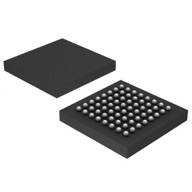
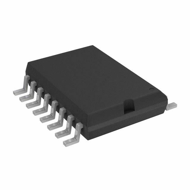
| 供应商器件封装 | 14-WSON (4x4) |
| 其它名称 | LMP91002SD/NOPBCT |
| 功率(W) | - |
| 包装 | 剪切带 (CT) |
| 封装/外壳 | 14-WFDFN 裸露焊盘 |
| 标准包装 | 1 |
| 电压-电源,数字 | - |
| 电压-电源,模拟 | 2.7 V ~ 3.6 V |
| 通道数 | 1 |


PDF Datasheet 数据手册内容提取
Product Sample & Technical Tools & Support & Folder Buy Documents Software Community LMP91002 SNIS163B–APRIL2012–REVISEDOCTOBER2015 LMP91002 Sensor AFE System: Configurable AFE Potentiostat for Low-Power Chemical Sensing Applications 1 Features 3 Description • TypicalValues,T =25°C The LMP91002 device is a programmable Analog 1 A Front End (AFE) for use in micro-power • SupplyVoltage2.7Vto3.6V electrochemical-sensing applications. It provides a • SupplyCurrent(AverageOverTime) <10µA complete signal path solution between a not biased • CellConditioningCurrentUpto10mA gas sensor and a microcontroller generating an outputvoltageproportionaltothecellcurrent. • ReferenceElectrodeBiasCurrent(85°C)900-pA (Maximum) The LMP91002’s programmability enables it support not biased electro-chemical gas sensor with a single • OutputDriveCurrent750µA design. The LMP91002 supports gas sensitivities • CompletePotentiostatCircuittoInterfacetoMost over a range of 0.5 nA/ppm to 9500 nA/ppm. It also NotBiasedGasSensors allows for an easy conversion of current ranges from • LowBiasVoltageDrift 5 μA to 750 μA full scale. The LMP91002’s • ProgrammableTIAGain2.75kΩto350kΩ transimpedance amplifier (TIA) gain is programmable through the I2C interface. The I2C interface can also • I2C-CompatibleDigitalInterface be used for sensor diagnostics. The LMP91002 is • AmbientOperatingTemperature –40°Cto85°C optimized for micro-power applications and operates • Package14-pinWSON over a voltage range of 2.7 V to 3.6 V. The total current consumption can be less than 10 μA. Further • SupportedbyWebenchSensorAFEDesigner power savings are possible by switching off the TIA amplifier and shorting the reference electrode to the 2 Applications workingelectrodewithaninternalswitch. • GasDetectors DeviceInformation(1) • AmperometricApplications PARTNUMBER PACKAGE BODYSIZE(NOM) • ElectrochemicalBloodGlucoseMeters LMP91002 WSON(14) 4.00mm×4.00mm (1) For all available packages, see the orderable addendum at theendofthedatasheet. TypicalApplication VREF VDD LMP91002 SCL I2C INTERFACE 3-Lead AND SDA MSP430 Electrochemical CONTROL REGISTERS Cell VREF CE + DIAGNOSTIC MENB A1 DIVIDER - CE RE RE DGND WE WE + VOUT TIA - RLoad RTIA C1 C2 AGND 1 An IMPORTANT NOTICE at the end of this data sheet addresses availability, warranty, changes, use in safety-critical applications, intellectualpropertymattersandotherimportantdisclaimers.PRODUCTIONDATA.
LMP91002 SNIS163B–APRIL2012–REVISEDOCTOBER2015 www.ti.com Table of Contents 1 Features.................................................................. 1 7.4 DeviceFunctionalModes........................................12 2 Applications........................................................... 1 7.5 Programming...........................................................12 3 Description............................................................. 1 7.6 RegisterMaps.........................................................14 4 RevisionHistory..................................................... 2 8 ApplicationandImplementation........................ 17 8.1 ApplicationInformation............................................17 5 PinConfigurationandFunctions......................... 3 8.2 TypicalApplication .................................................19 6 Specifications......................................................... 4 9 PowerSupplyRecommendations...................... 22 6.1 AbsoluteMaximumRatings......................................4 9.1 PowerConsumption................................................22 6.2 ESDRatings..............................................................4 10 Layout................................................................... 22 6.3 RecommendedOperatingConditions.......................4 6.4 ThermalInformation..................................................4 10.1 LayoutGuidelines.................................................22 6.5 ElectricalCharacteristics...........................................5 10.2 LayoutExample....................................................23 6.6 I2CInterface..............................................................6 11 DeviceandDocumentationSupport................. 25 6.7 TimingCharacteristics...............................................7 11.1 CommunityResources..........................................25 6.8 TypicalCharacteristics..............................................8 11.2 Trademarks...........................................................25 7 DetailedDescription............................................ 10 11.3 ElectrostaticDischargeCaution............................25 7.1 Overview.................................................................10 11.4 Glossary................................................................25 7.2 FunctionalBlockDiagram.......................................10 12 Mechanical,Packaging,andOrderable Information........................................................... 25 7.3 FeatureDescription.................................................10 4 Revision History NOTE:Pagenumbersforpreviousrevisionsmaydifferfrompagenumbersinthecurrentversion. ChangesfromRevisionA(March2013)toRevisionB Page • AddedESDRatingstable,FeatureDescriptionsection,DeviceFunctionalModes,ApplicationandImplementation section,PowerSupplyRecommendationssection,Layoutsection,DeviceandDocumentationSupportsection,and Mechanical,Packaging,andOrderableInformationsection.................................................................................................. 1 ChangesfromOriginal(March2013)toRevisionA Page • ChangedlayoutofNationalDataSheettoTIformat........................................................................................................... 18 2 SubmitDocumentationFeedback Copyright©2012–2015,TexasInstrumentsIncorporated ProductFolderLinks:LMP91002
LMP91002 www.ti.com SNIS163B–APRIL2012–REVISEDOCTOBER2015 5 Pin Configuration and Functions NHLPackage 14-PinWSON TopView DGND 1 14 CE MENB RE SCL WE SDA DAP VREF NC C1 VDD C2 AGND 7 8 VOUT PinFunctions(1) PIN I/O DESCRIPTION NO. NAME 1 DGND G Connecttoground 2 MENB D ModuleEnable.ActiveLow 3 SCL D I2CClock 4 SDA D I2CData 5 NC — Donotconnect.Notinternallyconnected 6 VDD P Voltagesupply 7 AGND GND AnalogGND 8 VOUT A Analogvoltagerepresentingsensoroutput 9 C2 A OptionalExternalcomponentnode2forTIA(filtercapacitororgainresistor) 10 C1 A OptionalExternalcomponentnode1forTIA(filtercapacitororgainresistor) 11 VREF A ExternalReferencevoltageinput 12 WE A WorkingElectrodeofthesensor. 13 RE A ReferenceElectrodeofthesensor. 14 CE A CounterElectrodeofthesensor. — DAP GND Dieattachedpad.ConnecttoGND. (1) A=analog,D=digital,P=power,G=GND Copyright©2012–2015,TexasInstrumentsIncorporated SubmitDocumentationFeedback 3 ProductFolderLinks:LMP91002
LMP91002 SNIS163B–APRIL2012–REVISEDOCTOBER2015 www.ti.com 6 Specifications 6.1 Absolute Maximum Ratings See (1)(2)(3) MIN MAX UNIT Voltagebetweenanytwopins 6 V CurrentthroughVDDorVSS 50 mA CurrentsunkandsourcedbyCEpin 10 mA Currentoutofotherpins(4) 5 mA Junctiontemperature(5) 150 °C Storagetemperature,T –65 150 °C stg (1) StressesbeyondthoselistedunderAbsoluteMaximumRatingsmaycausepermanentdamagetothedevice.Thesearestressratings only,whichdonotimplyfunctionaloperationofthedeviceattheseoranyotherconditionsbeyondthoseindicatedunderRecommended OperatingConditions.Exposuretoabsolute-maximum-ratedconditionsforextendedperiodsmayaffectdevicereliability. (2) Forsolderingspecifications,seeSNOA549. (3) IfMilitary/Aerospacespecifieddevicesarerequired,pleasecontacttheTexasInstrumentsSalesOffice/Distributorsforavailabilityand specifications. (4) Allnon-powerpinsofthisdeviceareprotectedagainstESDbysnapbackdevices.Voltageatsuchpinswillrisebeyondabsmaxif currentisforcedintopin. (5) ThemaximumpowerdissipationisafunctionofT ,θ ,andtheambienttemperature,T .Themaximumallowablepower J(MAX) JA A dissipationatanyambienttemperatureisP =(T -T )/θ AllnumbersapplyforpackagessoldereddirectlyontoaPCB. DMAX J(MAX) A JA 6.2 ESD Ratings VALUE UNIT Humanbodymodel(HBM),perANSI/ESDA/JEDECJS-001(1)(2) ±2000 V Electrostatic Charged-devicemodel(CDM),perJEDECspecificationJESD22-C101(3) ±1000 V (ESD) discharge MachineModel(MM) ±200 (1) JEDECdocumentJEP155statesthat500-VHBMallowssafemanufacturingwithastandardESDcontrolprocess. (2) HumanBodyModel,applicablestd.MIL-STD-883,Method3015.7.MachineModel,applicablestd.JESD22-A115-A(ESDMMstd.of JEDEC)Field-InducedCharge-DeviceModel,applicablestd.JESD22-C101-C(ESDFICDMstd.ofJEDEC). (3) JEDECdocumentJEP157statesthat250-VCDMallowssafemanufacturingwithastandardESDcontrolprocess. 6.3 Recommended Operating Conditions MIN MAX UNIT SupplyvoltageV =(VDD-AGND) 2.7 3.6 V S Temperature(1) –40 85 °C (1) ThemaximumpowerdissipationisafunctionofT ,θ ,andtheambienttemperature,T .Themaximumallowablepower J(MAX) JA A dissipationatanyambienttemperatureisP =(T -T )/θ AllnumbersapplyforpackagessoldereddirectlyontoaPCB. DMAX J(MAX) A JA 6.4 Thermal Information LMP91002 THERMALMETRIC(1) NHL(WSON) UNIT 14PINS R Junction-to-ambientthermalresistance (2) 44 °C/W θJA (1) Formoreinformationabouttraditionalandnewthermalmetrics,seetheSemiconductorandICPackageThermalMetricsapplication report,SPRA953. (2) ThemaximumpowerdissipationisafunctionofT ,θ ,andtheambienttemperature,T .Themaximumallowablepower J(MAX) JA A dissipationatanyambienttemperatureisP =(T -T )/θ AllnumbersapplyforpackagessoldereddirectlyontoaPCB. DMAX J(MAX) A JA 4 SubmitDocumentationFeedback Copyright©2012–2015,TexasInstrumentsIncorporated ProductFolderLinks:LMP91002
LMP91002 www.ti.com SNIS163B–APRIL2012–REVISEDOCTOBER2015 6.5 Electrical Characteristics Unlessotherwisespecified,alllimitsensuredforT =25°C,V =(V –AGND),V =3.3VandAGND=DGND=0V,V = A S DD S REF 2.5V,InternalZero=20%V .(1) REF PARAMETER TESTCONDITIONS MIN(2) TYP(3) MAX(2) UNIT POWERSUPPLYSPECIFICATION 3-leadamperometriccell TA=25ºC 10 13.5 mode Atthetemperature MODECN=0x03 extremes 15 T =25ºC 6.5 8 A Standbymode IS Supplycurrent MODECN=0x02 Atthetemperature 10 µA extremes T =25ºC 0.6 0.85 A Deepsleepmode MODECN=0x00 Atthetemperature 1 extremes POTENTIOSTAT T =25ºC –90 90 A VDD=2.7V; Internalzero50%VDD Atthetemperature –800 800 extremes I InputbiascurrentatREpin pA RE T =25ºC –90 90 A VDD=3.6V; Internalzero50%VDD Atthetemperature –900 900 extremes Minimumoperatingcurrent Sink 750 µA capability Source 750 I CE Minimumcharging Sink 10 capability(4) Source 10 mA Open-loopvoltagegainof 300mV≤VCE≤ TA=25ºC 120 AOL_A1 controlloopoperational Vs–300mV,–750µA≤ Atthetemperature dB amplifier(A1) ICE≤750µA extremes 104 Lowfrequencyintegrated en_RW noisebetweenREpinand 0.1Hzto10Hz(5) 3.4 µVpp WEpin 0%VREF,internalzero=20%VREF, –550 550 atthetemperatureextremes WEvoltageoffsetreferredto 0%VREF,internalzero=50%VREF, V –550 550 µV OS_RW RE atthetemperatureextremes 0%VREF,internalzero=67%VREF, –550 550 atthetemperatureextremes 0%VREF,internalzero=20%VREF –4 4 WEvoltageoffsetdrift TcV referredtoREfrom–40°Cto 0%VREF,internalzero=50%VREF –4 4 µV/°C OS_RW 85°C(6) 0%VREF,internalzero=67%VREF –4 4 (1) ElectricalTablevaluesapplyonlyforfactorytestingconditionsatthetemperatureindicated.Factorytestingconditionsresultinvery limitedself-heatingofthedevicesuchthatT =T .Noensuredspecificationofparametricperformanceisindicatedintheelectrical J A tablesunderconditionsofinternalself-heatingwhereT >T .AbsoluteMaximumRatingsindicatejunctiontemperaturelimitsbeyond J A whichthedevicemaybepermanentlydegraded,eithermechanicallyorelectrically. (2) Limitsare100%productiontestedat25°C.Limitsovertheoperatingtemperaturerangeareensuredthroughcorrelationsusing statisticalqualitycontrol(SQC)method. (3) Typicalvaluesrepresentthemostlikelyparametricnormasdeterminedatthetimeofcharacterization.Actualtypicalvaluesmayvary overtimeandwillalsodependontheapplicationandconfiguration.Thetypicalvaluesarenottestedandarenotensuredonshipped productionmaterial. (4) Atsuchcurrentsnoaccuracyoftheoutputvoltagecanbeexpected. (5) ThisparameterincludesbothA1andTIA'snoisecontribution. (6) OffsetvoltagetemperaturedriftisdeterminedbydividingthechangeinVOSatthetemperatureextremesbythetotaltemperature change.StartingfromthemeasuredvoltageoffsetattemperatureT1(V (T1)),thevoltageoffsetattemperatureT2(V (T2))is OS_RW OS_RW calculatedaccordingthefollowingformula:V (T2)=V (T1)+ABS(T2–T1)*TcV . OS_RW OS_RW OS_RW Copyright©2012–2015,TexasInstrumentsIncorporated SubmitDocumentationFeedback 5 ProductFolderLinks:LMP91002
LMP91002 SNIS163B–APRIL2012–REVISEDOCTOBER2015 www.ti.com Electrical Characteristics (continued) Unlessotherwisespecified,alllimitsensuredforT =25°C,V =(V –AGND),V =3.3VandAGND=DGND=0V,V = A S DD S REF 2.5V,InternalZero=20%V .(1) REF PARAMETER TESTCONDITIONS MIN(2) TYP(3) MAX(2) UNIT Transimpedancegain 5% accuracy Linearity ±0.05% 2.75 3.5 TIA_GAIN 7 7programmablegainresistors 14 ProgrammableTIAgains 35 kΩ 120 350 Maximumexternalgainresistor 350 20% 3programmablepercentagesofVREF 50% 67% Internalzerovoltage 20% TIA_ZV 3programmablepercentagesofVDD 50% 67% Internalzerovoltage ±0.04% accuracy Loadresistor 10 Ω RL Loadaccuracy 5% Internalzero20%VREF 80 110 Powersupplyrejectionratio PSRR 2.7V≤VDD≤5.25V Internalzero50%VREF 80 110 dB atREpin Internalzero67%VREF 80 110 EXTERNALREFERENCESPECIFICATION(7) Externalvoltagereference 1.5 VDD V VREF range Inputimpedance 10 MΩ (7) Incaseofexternalreferenceconnected,thenoiseofthereferencehastobeadded. 6.6 I2C Interface Unlessotherwisespecified,alllimitsensuredforatT =25°C,V =(VDD–AGND),2.7V<V <3.6VandAGND=DGND=0 A S S V,VREF=2.5V.(1) PARAMETER TESTCONDITIONS MIN(2) TYP(3) MAX(2) UNIT V InputHighVoltage Atthetemperatureextremes 0.7*VDD V IH V InputLowVoltage Atthetemperatureextremes 0.3*VDD V IL I =3mA,atthetemperature V OutputLowVoltage OUT 0.4 V OL extremes Hysteresis(4) Atthetemperatureextremes 0.1*VDD V C InputCapacitanceonalldigitalpins Atthetemperatureextremes 0.5 pF IN (1) ElectricalTablevaluesapplyonlyforfactorytestingconditionsatthetemperatureindicated.Factorytestingconditionsresultinvery limitedself-heatingofthedevicesuchthatT =T .Noensuredspecificationofparametricperformanceisindicatedintheelectrical J A tablesunderconditionsofinternalself-heatingwhereT >T .AbsoluteMaximumRatingsindicatejunctiontemperaturelimitsbeyond J A whichthedevicemaybepermanentlydegraded,eithermechanicallyorelectrically. (2) Limitsare100%productiontestedat25°C.Limitsovertheoperatingtemperaturerangeareensuredthroughcorrelationsusing statisticalqualitycontrol(SQC)method. (3) Typicalvaluesrepresentthemostlikelyparametricnormasdeterminedatthetimeofcharacterization.Actualtypicalvaluesmayvary overtimeandwillalsodependontheapplicationandconfiguration.Thetypicalvaluesarenottestedandarenotensuredonshipped productionmaterial. (4) Thisparameterisspecifiedbydesignorcharacterization. 6 SubmitDocumentationFeedback Copyright©2012–2015,TexasInstrumentsIncorporated ProductFolderLinks:LMP91002
LMP91002 www.ti.com SNIS163B–APRIL2012–REVISEDOCTOBER2015 6.7 Timing Characteristics Unlessotherwisespecified,alllimitsensuredforT =25°C,V =(VDD–AGND),V =3.3VandAGND=DGND=0V,VREF A S S =2.5V,InternalZero=20%VREF.Alllimitsapplyatthetemperatureextremes.RefertotimingdiagraminFigure1(1). PARAMETER TESTCONDITIONS MIN TYP MAX UNIT f ClockFrequency Atthetemperatureextremes 10 100 kHz SCL t ClockLowTime Atthetemperatureextremes 4.7 µs LOW t ClockHighTime Atthetemperatureextremes 4 µs HIGH Afterthisperiod,thefirstclockpulseis t Datavalid 4 µs HD;STA generatedatthetemperatureextremes Set-uptimeforarepeatedSTART t Atthetemperatureextremes 4.7 µs SU;STA condition t Dataholdtime(2) Atthetemperatureextremes 0 ns HD;DAT t DataSet-uptime Atthetemperatureextremes 250 ns SU;DAT t SDAfalltime(3) IL≤3mA,CL≤400pF, 250 ns f atthetemperatureextremes t Set-uptimeforSTOPcondition Atthetemperatureextremes 4 µs SU;STO BusfreetimebetweenaSTOPand t Atthetemperatureextremes 4.7 µs BUF STARTcondition t Datavalidtime Atthetemperatureextremes 3.45 µs VD;DAT t Datavalidacknowledgetime Atthetemperatureextremes 3.45 µs VD;ACK Pulsewidthofspikesthatmustbe tSP suppressedbytheinputfilter(3) Atthetemperatureextremes 50 ns t_timeout SCLandSDATimeout Atthetemperatureextremes 25 100 ms t I2CInterfaceEnabling Atthetemperatureextremes 600 ns EN;START t I2CInterfaceDisabling Atthetemperatureextremes 600 ns EN;STOP timebetweenconsecutiveI2C t Atthetemperatureextremes 600 ns EN;HIGH interfaceenablinganddisabling (1) ElectricalTablevaluesapplyonlyforfactorytestingconditionsatthetemperatureindicated.Factorytestingconditionsresultinvery limitedself-heatingofthedevicesuchthatT =T .Noensuredspecificationofparametricperformanceisindicatedintheelectrical J A tablesunderconditionsofinternalself-heatingwhereT >T .AbsoluteMaximumRatingsindicatejunctiontemperaturelimitsbeyond J A whichthedevicemaybepermanentlydegraded,eithermechanicallyorelectrically. (2) LMP91002providesaninternal300nsminimumholdtimetobridgetheundefinedregionofthefallingedgeofSCL. (3) Thisparameterisspecifiedbydesignorcharacterization. MENB70% 30% tEN;START tEN;STOP tEN;HIGH SDA 70% 30% tf tLOW tVD;DAT tHD;STA tBUF tSP 70% SCL 30% tHD;STA tSU;STA tSU;STO tHIGH tHD;DAT tSU;DAT tVD;ACK START 1/fSCL REPEATED STOP START START Figure1. I2CInterfaceTimingDiagram Copyright©2012–2015,TexasInstrumentsIncorporated SubmitDocumentationFeedback 7 ProductFolderLinks:LMP91002
LMP91002 SNIS163B–APRIL2012–REVISEDOCTOBER2015 www.ti.com 6.8 Typical Characteristics Unlessotherwisespecified,T =25°C,V =(VDD–AGND),2.7V<V <3.6VandAGND=DGND=0V,VREF=2.5V. A S S -100 -100 VDD = 2.7V 85°C -120 VDD = 3.3V -120 25°C -40°C -140 -140 -160 -160 V) -180 V) -180 (cid:29) (cid:29) S ( -200 S ( -200 O O V -220 V -220 -240 -240 -260 -260 -280 -280 -300 -300 -50 -25 0 25 50 75 100 2.7 2.8 2.9 3.0 3.1 3.2 3.3 3.4 3.5 3.6 TEMPERATURE (°C) SUPPLY VOLTAGE (V) Figure2.InputV vsTemperature Figure3.InputV vsVDD OS_RW OS_RW 140 1.0 VDD = 2.7V VDD = 3.3V 0.9 130 A) 0.8 (cid:29) 120 T ( 0.7 B) EN R (d 110 RR 0.6 SR CU 0.5 P Y 100 L 0.4 P P U 0.3 S 90 0.2 80 0.1 10 100 1k 10k 100k -50 -25 0 25 50 75 100 FREQUENCY (Hz) TEMPERATURE (°C) Figure4.ACPSRRvsFrequency Figure5.SupplyCurrentvsTemperature(DeepSleepMode) 1.0 7.50 85°C VDD = 2.7V 25°C VDD = 3.3V 0.9 -40°C 7.25 A) 0.8 A) (cid:29) (cid:29) 7.00 T ( 0.7 T ( N N 6.75 E E R 0.6 R R R 6.50 U U C 0.5 C Y Y 6.25 L 0.4 L P P UP 0.3 UP 6.00 S S 0.2 5.75 0.1 5.50 2.7 2.8 2.9 3.0 3.1 3.2 3.3 3.4 3.5 3.6 -50 -25 0 25 50 75 100 SUPPLY VOLTAGE (V) TEMPERATURE (°C) Figure6.SupplyCurrentvsVDD(DeepSleepMode) Figure7.SupplyCurrentvsTemperature(StandbyMode) 8 SubmitDocumentationFeedback Copyright©2012–2015,TexasInstrumentsIncorporated ProductFolderLinks:LMP91002
LMP91002 www.ti.com SNIS163B–APRIL2012–REVISEDOCTOBER2015 Typical Characteristics (continued) Unlessotherwisespecified,T =25°C,V =(VDD–AGND),2.7V<V <3.6VandAGND=DGND=0V,VREF=2.5V. A S S 7.50 11.0 85°C VDD = 2.7V 25°C 10.8 VDD = 3.3V 7.25 -40°C VDD = 5V A) A) 10.6 (cid:29) 7.00 (cid:29) T ( T ( 10.4 N 6.75 N E E 10.2 R R R 6.50 R 10.0 U U C C Y 6.25 Y 9.8 L L P P 9.6 UP 6.00 UP S S 9.4 5.75 9.2 5.50 9.0 2.7 2.8 2.9 3.0 3.1 3.2 3.3 3.4 3.5 3.6 -50 -25 0 25 50 75 100 SUPPLY VOLTAGE (V) TEMPERATURE (°C) Figure8.SupplyCurrentvsVDD(StandbyMode) Figure9.SupplyCurrentvsTemperature(3-Lead AmperometricMode) 11.0 1.5 85°C 10.8 25°C -40°C 1.0 A) 10.6 (cid:29) NT ( 10.4 V) 0.5 E 10.2 (cid:29) RR 10.0 W ( 0.0 U R C _ LY 9.8 EN -0.5 P 9.6 P U S 9.4 -1.0 9.2 9.0 -1.5 2.7 2.8 2.9 3.0 3.1 3.2 3.3 3.4 3.5 3.6 0 1 2 3 4 5 6 7 8 9 10 SUPPLY VOLTAGE (V) TIME (s) Figure10.SupplyCurrentvsVDD(3-LeadAmperometric Figure11.0.1-Hzto10-HzNoise Mode) Copyright©2012–2015,TexasInstrumentsIncorporated SubmitDocumentationFeedback 9 ProductFolderLinks:LMP91002
LMP91002 SNIS163B–APRIL2012–REVISEDOCTOBER2015 www.ti.com 7 Detailed Description 7.1 Overview The LMP91002 is a programmable AFE for use in micropower chemical sensing applications. The LMP91002 is designed for 3-lead non-biased gas sensors and for 2 leads galvanic cell. This device provides all of the functionality for detecting changes in gas concentration based on a delta current at the working electrode. The LMP91002 generates an output voltage proportional to the cell current. Transimpedance gain is user programmable through an I2C compatible interface from 2.75kΩ to 350kΩ making it easy to convert current ranges from 5µA to 750µA full scale. Optimized for micro-power applications, the LMP91002 AFE works over a voltage range of 2.7V to 3.6 V. The cell voltage is user selectable using the on board programmability. In addition, it is possible to connect an external transimpedance gain resistor. Depending on the configuration, total current consumption for the device can be less than 10µA. For power savings, the transimpedance amplifier can beturnedoffandinsteadaloadimpedanceequivalenttotheTIA’sinputsimpedanceisswitchedin. 7.2 Functional Block Diagram VREF VDD LMP91002 SCL I2C INTERFACE 3-Lead AND SDA Electrochemical CONTROL REGISTERS Cell VREF CE A1 + DIAGNOSTIC DIVIDER MENB - CE RE RE DGND WE WE + TIA VOUT - RLoad RTIA C1 C2 AGND 7.3 Feature Description 7.3.1 PotentiostatCircuitry The core of the LMP91002 is a potentiostat circuit. It consists of a differential input amplifier used to compare the potentialbetweentheworkingandreferenceelectrodestoazerobiaspotential..Theerrorsignalisamplifiedand applied to the counter electrode (through the Control Amplifier - A1). Any changes in the impedance between theworkingandreferenceelectrodeswillcauseachangeinthevoltageappliedtothecounterelectrode,inorder to maintain the constant voltage between working and reference electrodes. A Transimpedance Amplifier connected to the working electrode, is used to provide an output voltage that is proportional to the cell current. The working electrode is held at virtual ground (Internal ground) by the transimpedance amplifier. The potentiostat will compare the reference voltage to the desired bias potential and adjust the voltage at the counter electrodetomaintaintheproperworking-to-referencevoltage. 7.3.2 TransimpedanceAmplifier Thetransimpedanceamplifier(TIAinFunctionalBlockDiagram)has7programmableinternalgainresistors.This accommodates the full scale ranges of most existing sensors. Moreover an external gain resistor can be connectedtotheLMP91002betweenC1andC2pins.ThegainissetthroughtheI2Cinterface. 10 SubmitDocumentationFeedback Copyright©2012–2015,TexasInstrumentsIncorporated ProductFolderLinks:LMP91002
LMP91002 www.ti.com SNIS163B–APRIL2012–REVISEDOCTOBER2015 Feature Description (continued) 7.3.3 ControlAmplifier The control amplifier (A1 op amp in Functional Block Diagram) provides initial charge to the sensor. A1 has the capability to drive up to 10mA into the sensor in order to to provide a fast initial conditioning. A1 is able to sink and source current according to the connected gas sensor (reducing or oxidizing gas sensor). It can be powered down to reduce system power consumption. However powering down A1 is not recommended, as it may take a longtimeforthesensortorecoverfromthissituation. 7.3.4 InternalZero The internal Zero is the voltage at the non-inverting pin of the TIA. The internal zero can be programmed to be either 67%, 50% or 20%, of the supply, or the external reference voltage. This provides both sufficient headroom for the counter electrode of the sensor to swing, in case of sudden changes in the gas concentration, and best useoftheADC’sfullscaleinputrange. The Internal zero is provided through an internal voltage divider (Vref divider box in Functional Block Diagram). ThedividerisprogrammedthroughtheI2Cinterface. 7.3.5 2-LeadGalvanicCellinPotentiostatConfiguration When the LMP91002 is interfaced to a galvanic cell (for instance to an Oxygen gas sensor) referred to a reference, the Counter and the Reference pin of the LMP91002 are shorted together and connected to negative electrode of the galvanic cell. The positive electrode of the galvanic cell is then connected to the Working pin of theLMP91002. The LMP91002 is then configured in 3-lead amperometric cell mode (as for amperometric cell). In this configuration the Control Amplifier (A1) is ON and provides the internal zero voltage. The transimpedance amplifier (TIA) is also ON, it converts the current generated by the gas sensor in a voltage, according to the transimpedancegain: Gain=R TIA If different gains are required, an external resistor can be connected between the pins C1 and C2. In this case theinternalfeedbackresistorshouldbeprogrammedto“external”. VREF VDD SCL LMP91002 I2C INTERFACE AND SDA 2-Lead Sensor CONTROL such as Oxygen REGISTERS CE A1 + DIAGNOSTIC DVIVRIDEEFR MENB - VE- RE NC DGND VE+ WE + TIA VOUT RLoad - RTIA C1 C2 AGND Figure12. Two-LeadSensorConnections Copyright©2012–2015,TexasInstrumentsIncorporated SubmitDocumentationFeedback 11 ProductFolderLinks:LMP91002
LMP91002 SNIS163B–APRIL2012–REVISEDOCTOBER2015 www.ti.com 7.4 Device Functional Modes 7.4.1 TimeoutFeature The timeout is a safety feature to avoid bus lockup situation. If SCL is stuck low for a time exceeding t_timeout, theLMP91002willautomaticallyresetitsI2Cinterface.Also,inthecasetheLMP91002hangstheSDAforatime exceeding t_timeout, the LMP91002’s I2C interface will be reset so that the SDA line will be released. Since the SDAisanopen-drainwithanexternalresistorpull-up,thisalsoavoidshighpowerconsumptionwhenLMP91002 isdrivingthebusandtheSCLisstopped. 7.5 Programming 7.5.1 I2CInterface The I2C compatible interface operates in Standard mode (100kHz). Pull-up resistors or current sources are required on the SCL and SDA pins to pull them high when they are not being driven low. A logic zero is transmitted by driving the output low. A logic high is transmitted by releasing the output and allowing it to be pulled-up externally. The appropriate pull-up resistor values will depend upon the total bus capacitance and operatingspeed.TheLMP91002comeswitha7bitbusfixedaddress:1001000. 7.5.2 WriteandReadOperation In order to start any read or write operation with the LMP91002, MENB needs to be set low during the whole communication. Then the master generates a start condition by driving SDA from high to low while SCL is high. The start condition is always followed by a 7-bit slave address and a Read/Write bit. After these 8 bits have been transmitted by the master, SDA is released by the master and the LMP91002 either ACKs or NACKs the address. If the slave address matches, the LMP91002 ACKs the master. If the address doesn't match, the LMP91002 NACKs the master. For a write operation, the master follows the ACK by sending the 8-bit register address pointer. Then the LMP91002 ACKs the transfer by driving SDA low. Next, the master sends the 8-bit data to the LMP91002. Then the LMP91002 ACKs the transfer by driving SDA low. At this point the master shouldgenerateastopconditionandoptionallysettheMENBatlogichighlevel(refertoFigure15). A read operation requires the LMP91002 address pointer to be set first, also in this case the master needs setting at low logic level the MENB, then the master needs to write to the device and set the address pointer before reading from the desired register. This type of read requires a start, the slave address, a write bit, the address pointer, a Repeated Start (if appropriate), the slave address, and a read bit (refer to Figure 15). Followingthissequence,theLMP91002sendsoutthe8-bitdataoftheregister. WhenjustoneLMP91002ispresentontheI2CbustheMENBcanbetiedtoground(lowlogiclevel). MENB 1 9 1 9 SCL SDA A6 A5 A4 A3 A2 A1 A0 R/W D7 D6 D5 D4 D3 D2 D1 D0 Start by Ack Ack Master by by Frame 1 LMP91000 Frame 2 LMP91000 Serial Bus Address Byte Internal Address Register from Master Byte from Master MENB (continued) 1 9 SCL (continued) SDA D7 D6 D5 D4 D3 D2 D1 D0 (continued) Ack Stop by by Master LMP91000 Frame 3 Data Byte Figure13. (a)RegisterWriteTransaction 12 SubmitDocumentationFeedback Copyright©2012–2015,TexasInstrumentsIncorporated ProductFolderLinks:LMP91002
LMP91002 www.ti.com SNIS163B–APRIL2012–REVISEDOCTOBER2015 Programming (continued) MENB 1 9 1 9 SCL SDA A6 A5 A4 A3 A2 A1 A0 R/W D7 D6 D5 D4 D3 D2 D1 D0 Start by Ack Ack Stop by Master by by Master Frame 1 LMP91000 Frame 2 LMP91000 Serial Bus Address Byte Internal Address Register from Master Byte from Master Figure14. (b)PointerSetTransaction MENB 1 9 1 9 SCL SDA A6 A5 A4 A3 A2 A1 A0 R/W D7 D6 D5 D4 D3 D2 D1 D0 Start by Ack No Ack Stop Master by by by Frame 1 LMP91000 Frame 2 Master Master Serial Bus Address Byte Data Byte from from Master Slave (c)Registerreadtransaction Figure15. READandWRITETransaction 7.5.3 ConnectionofMoreThanOneLMP91002totheI2CBus The LMP91002 comes out with a unique and fixed I2C slave address. It is still possible to connect more than one LMP91002 to an I2C bus and select each device using the MENB pin. The MENB simply enables/disables the I2C communication of the LMP91002. When the MENB is at logic level low all the I2C communication is enabled, itisdisabledwhenMENBisathighlogiclevel. In a system based on a μcontroller and more than one LMP91002 connected to the I2C bus, the I2C lines (SDA and SCL) are shared, while the MENB of each LMP91002 is connected to a dedicate GPIO port of the μcontroller. The μcontroller starts communication asserting one out of N MENB signals where N is the total number of LMP91002s connected to the I2C bus. Only the enabled device will acknowledge the I2C commands. After finishing communicating with this particular LMP91002, the microcontroller de-asserts the corresponding MENB and repeats the procedure for other LMP91002s. Figure 16 shows the typical connection when more than one LMP91002isconnectedtotheI2Cbus. LMP91000 LMP91000 LMP91000 LMP91000 B B B B EN CL DA EN CL DA EN CL DA EN CL DA M S S M S S M S S M S S GPIO 1 GPIO 2 GPIO 3 GPIO N SCL µC SDA Figure16. MorethanoneLMP91002onI2Cbus Copyright©2012–2015,TexasInstrumentsIncorporated SubmitDocumentationFeedback 13 ProductFolderLinks:LMP91002
LMP91002 SNIS163B–APRIL2012–REVISEDOCTOBER2015 www.ti.com 7.6 Register Maps TheregistersareusedtoconfiguretheLMP91002. Ifwritingtoareservedbit,usermustwriteonly0.Readbackvalueisunspecifiedandshouldbediscarded. Table1.RegisterMap Offset Name PoweronDefault Access(1) Lockable? Section 00h STATUS 0x00 Readonly N Go 01h LOCK 0x01 R/W N Go 02hthrough09h RESERVED 10h TIACN 0x03 R/W Y Go 11h REFCN 0x20 R/W Y Go 12h MODECN 0x00 R/W N Go 13hthroughFFh RESERVED (1) LEGEND:R/W=Read/Write;R=Readonly;-n=valueafterreset 7.6.1 STATUSRegister(Offset=00h) Status Register. The status bit is an indication of the LMP91002's power-on status. If its readback is “0”, the LMP91002isnotreadytoacceptotherI2Ccommands. Figure17. STATUSRegister 7 6 5 4 3 2 1 0 Reserved STATUS R R Table2.STATUSRegisterFieldDescriptions Bit Name Function 7-1 RESERVED StatusofDevice 0 STATUS 0h=NotReady(default) 1h=Ready 7.6.2 LOCKRegister(Offset=01h) Protection Register. The lock bit enables and disables the writing of the TIACN and the REFCN registers. To changethecontentoftheTIACNandtheREFCNregisters,thelockbitmustbesetto “0”. Figure18. LOCKRegister 7 6 5 4 3 2 1 0 Reserved LOCK R/W Table3.LOCKRegisterFieldDescriptions Bit Name Function 7-1 RESERVED Writeprotection 0 LOCK 0h=Registers0x10,0x11inwritemode 1h=Registers0x10,0x11inreadonlymode(default) 14 SubmitDocumentationFeedback Copyright©2012–2015,TexasInstrumentsIncorporated ProductFolderLinks:LMP91002
LMP91002 www.ti.com SNIS163B–APRIL2012–REVISEDOCTOBER2015 7.6.3 TIACNRegister(Offset=10h) TIA Control Register. The parameters in the TIA control register allow the configuration of the transimpedance gain(R ). TIA Figure19. TIACNRegister 7 6 5 4 3 2 1 0 Reserved TIA_GAIN Reserved Table4.TIACNRegisterFieldDescriptions Bit Name Function 7-5 RESERVED RESERVED TIAfeedbackresistanceselection 000h=Externalresistance(default) 001h=2.75kΩ 010h=3.5kΩ 4-2 TIA_GAIN 011h=7kΩ 100h=14kΩ 101h=35kΩ 110h=120kΩ 111h=350kΩ 1-0 RESERVED RESERVED 7.6.4 REFCNRegister(Offset=11h) Reference Control Register. The parameters in the Reference control register allow the configuration of the Internal zero, and reference source. When the reference source is external, the reference is provided by a reference voltage connected to the VREF pin. In this condition the internal zero is defined as a percentage of VREFvoltageinsteadofthesupplyvoltage. Figure20. REFCNRegister 7 6 5 4 3 2 1 0 REF_SOURCE INT_Z Reserved DIAGNOSTIC Table5.REFCNRegisterFieldDescriptions BIT NAME FUNCTION Referencevoltagesourceselection 7 REF_SOURCE 0h=Internal(default) 1h=external Internalzeroselection(Percentageofthesourcereference) 00h=20% 6-5 INT_Z 01h=50%(default) 10h=67% 4 RESERVED RESERVED Diagnosticstep(Percentageofthesourcereference) 3-0 DIAGNOSTIC 0000h=0%(default) 0001h=1% Copyright©2012–2015,TexasInstrumentsIncorporated SubmitDocumentationFeedback 15 ProductFolderLinks:LMP91002
LMP91002 SNIS163B–APRIL2012–REVISEDOCTOBER2015 www.ti.com 7.6.5 MODECNRegister(Offset=12h) Mode Control Register. The parameters in the mode register allow the configuration of the operation mode of the LMP91002. Figure21. MODECNRegister 7 6 5 4 3 2 1 0 FET_SHORT Reserved OP_MODE Table6.MODECNRegisterFieldDescriptions BIT NAME FUNCTION ShortingFETfeature 7 FET_SHORT 0h=Disabled(default) 1h=Enabled 6-3 RESERVED RESERVED ModeofOperationselection 000h=DeepSleep(default) 2-0 OP_MODE 010h=Standby 011h=3-leadamperometriccell 16 SubmitDocumentationFeedback Copyright©2012–2015,TexasInstrumentsIncorporated ProductFolderLinks:LMP91002
LMP91002 www.ti.com SNIS163B–APRIL2012–REVISEDOCTOBER2015 8 Application and Implementation NOTE Information in the following applications sections is not part of the TI component specification, and TI does not warrant its accuracy or completeness. TI’s customers are responsible for determining suitability of components for their purposes. Customers should validateandtesttheirdesignimplementationtoconfirmsystemfunctionality. 8.1 Application Information 8.1.1 GasSensorInterface The LMP91002 supports both 3-lead and 2-lead gas sensors. Most of the toxic gas sensors are amperometric cells with 3 leads (Counter, Worker and Reference). These leads should be connected to the LMP91002 in the potentiostattopology. 8.1.1.1 3-LeadAmperometricCellInPotentiostatConfiguration Most of the amperometric cell have 3 leads (Counter, Reference and Working electrodes). The interface of the 3- lead gas sensor to the LMP91002 is straightforward. The leads of the gas sensor should be connected to the LMP91002pinswhichhavethematchingname The LMP91002 is then configured in 3-lead amperometric cell mode; in this configuration the Control Amplifier (A1) is ON and provides the internal zero voltage and bias in case of biased gas sensor. The transimpedance amplifier (TIA) is ON, it converts the current generated by the gas sensor in a voltage, according to the transimpedancegain: Gain=R TIA If different gains are required, an external resistor can be connected between the pins C1 and C2. In this case the internal feedback resistor should be programmed to “external”. The R together with the output Load capacitanceofthegassensoractsasalowpassfilter. VREF VDD LMP91002 SCL I2C INTERFACE 3-Lead AND SDA Electrochemical CONTROL REGISTERS Cell VREF CE A1 + DIAGNOSTIC DIVIDER MENB - CE RE RE DGND WE WE + TIA VOUT - RLoad RTIA C1 C2 AGND Figure22. 3-LeadAmperometricCell Copyright©2012–2015,TexasInstrumentsIncorporated SubmitDocumentationFeedback 17 ProductFolderLinks:LMP91002
LMP91002 SNIS163B–APRIL2012–REVISEDOCTOBER2015 www.ti.com Application Information (continued) 8.1.2 SensorTestProcedure The LMP91002 has all the hardware and programmability features to implement some test procedures. The purposeofthetestprocedureisto: a. testproperfunctionofthesensor(statusofhealth) b. testproperconnectionofthesensortotheLMP91002 The test procedure is very easy. The diagnostic block is user programmable through the digital interface. A step voltage can be applied by the end user to the positive input of A1. As a consequence a transient current will start flowing into the sensor (to charge its internal capacitance) and it will be detected by the TIA. If the current transient is not detected, either a sensor fault or a connection problem is present. The slope and the aspect of the transient response can also be used to detect sensor aging (for example, a cell that is drying and no longer efficientlyconductsthecurrent).Afteritisverifiedthatthesensorisworkingproperly,theLMP91002needstobe reset to its original configuration. It is not required to observe the full transient in order to contain the testing time. All the needed information are included in the transient slopes (both edges). Figure 23 shows an example test procedure, a Carbon Monoxide sensor is connected to the LMP91002, a 25-mVpp pulse is applied between ReferenceandWorkingpin. Thefollowingprocedureshowshowtoimplementthesensortest.Preliminaryconditions: TheLMP91002isunlockedanditisin3-LeadAmperometricCellMode 1. Put in the [3:0] bit of the register REFCN (0x11) the 0001b value, leaving the other bit unchanged. This operationwillapplyapotential(V )betweenREandWEpin(V >V ),V =1%Sourcereference. RW RE WE RW 2. Put in the [3:0] bit of the register REFCN (0x11) the 0000b value, leaving the other bit unchanged. This operationwillremovethepotential(V )betweenREandWEpin(V >V ),V =0V. RW RE WE RW Thewidthofthepulseissimplythetimebetweenthetwowritingoperation. LMP91000 OUTPUT TEST PULSE V) DI V/ V) m DI 500 mV/ E ( 50 LTTAG ULSE ( O P V T T U U P P N T I U O TIME (25ms/DIV) Figure23. TestProcedureExample 18 SubmitDocumentationFeedback Copyright©2012–2015,TexasInstrumentsIncorporated ProductFolderLinks:LMP91002
LMP91002 www.ti.com SNIS163B–APRIL2012–REVISEDOCTOBER2015 8.2 Typical Application VREF VDD LMP91002 SCL I2C INTERFACE 3-Lead AND SDA MSP430 Electrochemical CONTROL REGISTERS Cell VREF CE + DIAGNOSTIC MENB A1 DIVIDER - CE RE RE DGND WE WE + VOUT TIA - RLoad RTIA C1 C2 AGND Figure24. AFEGasDetector 8.2.1 DesignRequirements The primary design requirement is selecting the appropriate TIA gain for the expected range of current over the operating range of the sensor. This gain should set the VOUT range to fall within the limits of the full-scale voltage for the ADC that is sampling the signal. For example, assume the current output range of the sensor is 0 to 100,000 nA, and the full scale ADC input range is 0 to 1 V. Because Gain = R , the appropriate relationship TIA is: ISENSOR×Gain=R ×10–4A≤1V (1) TIA Hence, R < 104 Ω. In this case, the closest programmed gain value is 7 kΩ (see Table 4). However, if TIA optimization of the full-scale range is desired, then alternatively, R can be programmed to 350 kΩ, and a 10- TIA kΩresistorconnectedbetweenpinsC1andC2.Thiswillgiveanequivalentresistanceof9.7kΩ. 8.2.2 DetailedDesignProcedure 8.2.2.1 SmartGasSensorAnalogFrontEnd The LMP91002 together with an external EEPROM represents the core of a SMART GAS SENSOR AFE. In the EEPROM it is possible to store the information related to the GAS sensor type, calibration and LMP91002's configuration (content of registers 10h, 11h, 12h). At startup the microcontroller reads the EEPROM's content and configures the LMP91002. A typical smart gas sensor AFE is shown in Figure 25. The connection of MENB to the hardware address pin A0 of the EEPROM allows the microcontroller to select the LMP91002 and its correspondingEEPROMwhenmorethanonesmartgassensorAFEispresentontheI2Cbus. NOTE OnlyEEPROMI2CaddresseswithA0=0shouldbeusedinthisconfiguration. Copyright©2012–2015,TexasInstrumentsIncorporated SubmitDocumentationFeedback 19 ProductFolderLinks:LMP91002
LMP91002 SNIS163B–APRIL2012–REVISEDOCTOBER2015 www.ti.com Typical Application (continued) LMP91000 I2C EEPROM B MEN SCL SDA A0 SCL SDA MENB SCL SDA Figure25. SmartGasSensorAFE 8.2.2.2 SmartGasSensorAFESonI2CBus The connection of Smart gas sensor AFEs on the I2C bus is the natural extension of the previous concepts. Also in this case the microcontroller starts communication asserting 1 out of N MENB signals where N is the total number of smart gas sensor AFE connected to the I2C bus. Only one of the devices (either LMP91002 or its corresponding EEPROM) in the smart gas sensor AFE enabled will acknowledge the I2C commands. When the communication with this particular module ends, the microcontroller de-asserts the corresponding MENB and repeats the procedure for other modules. Figure 26 shows the typical connection when several smart gas sensor AFEsareconnectedtotheI2Cbus. LMP91000 I2C EEPROM LMP91000 I2C EEPROM LMP91000 I2C EEPROM B B B MEN SCL SDA A0 SCL SDA MEN SCL SDA A0 SCL SDA MEN SCL SDA A0 SCL SDA SMART SENSOR AFE SMART SENSOR AFE SMART SENSOR AFE GPIO 1 GPIO 2 GPIO N SCL µC SDA Figure26. SmartGasSensorAFEsonI2CBus 20 SubmitDocumentationFeedback Copyright©2012–2015,TexasInstrumentsIncorporated ProductFolderLinks:LMP91002
LMP91002 www.ti.com SNIS163B–APRIL2012–REVISEDOCTOBER2015 Typical Application (continued) 8.2.3 ApplicationCurves V) V) DI DI V/ V/ m I m I 0 WE TPUT (200 WE (cid:29)A/DIV) UT TIA (20 237..k75(cid:13)k5(cid:13)k(cid:13) (cid:29)A/DIV) D OU 23..75k5(cid:13)k(cid:13) (50WE OUTP 1314520kk(cid:13)(cid:13)k(cid:13) (50WE ZE 71k4(cid:13)k(cid:13) I D 350k(cid:13) I LI 35k(cid:13) ZE MA 120k(cid:13) LI 350k(cid:13) A R M O R N O N TIME (200(cid:29)s/DIV) TIME (200(cid:29)s/DIV) Figure27.I StepCurrentResponse(Rise) Figure28.I StepCurrentResponse(Fall) WE WE 2.0 LMP91000 1.9 1.8 1.7 V) 1.6 T ( U 1.5 O V 1.4 1.3 1.2 RTIA=35k(cid:13), 1.1 Rload=10(cid:13), 1.0 0 25 50 75 100 125 150 TIME (s) Figure29.AVOUTStepResponse100ppmto400ppmCO (COGasSensorConnectedtoLMP91002) Copyright©2012–2015,TexasInstrumentsIncorporated SubmitDocumentationFeedback 21 ProductFolderLinks:LMP91002
LMP91002 SNIS163B–APRIL2012–REVISEDOCTOBER2015 www.ti.com 9 Power Supply Recommendations 9.1 Power Consumption The LMP91002 is intended for use in portable devices, so the power consumption is as low as possible in order to ensure a long battery life. The total power consumption for the LMP91002 is below 10 µA at 3.3-V average over time, (this excludes any current drawn from any pin). A typical usage of the LMP91002 is in a portable gas detectoranditspowerconsumptionissummarizedinTable7.Thishasthefollowingassumptions: • PowerOnonlyhappensafewtimesoverlife,soitspowerconsumptioncanbeignored • DeepSleepmodeisnotused • Thesystemisusedabout8hoursaday,and16hoursadayitisinStandbymode. This results in an average power consumption of approximately 7.8 µA. This can potentially be further reduced, by using the Standby mode between gas measurements. It may even be possible, depending on the sensor used, to go into deep sleep for some time between measurements, further reducing the average power consumption. Table7.PowerConsumptionScenario 3-LEADAMPEROMETRIC DEEPSLEEP STANDBY TOTAL CELL Currentconsumption(µA)typicalvalue 0.6 6.5 10 TimeON(%) 0 60 39 Average(µA) 0 3.9 3.9 7.8 Notes A1 OFF ON ON TIA OFF OFF ON I2Cinterface ON ON ON 10 Layout 10.1 Layout Guidelines Figure 30 and Figure 31 show an example layout for the LMP91002. Figure 30 shows the top layer, and Figure 31 shows the bottom layer. Figure 30 shows that the sensor electrodes may be arranged around the LMP91002 so that the sensor sets directly over the LMP91002, creating a compact layout. There are very few components needed for the LMP91002: one or more bypass capacitors attached to VDD, and one or two optional external components attached to pins C1 or C2 of the TIA that can provide extra filtering or gain. In the layout shown here, the VDD bypass capacitor is on the top layer, close to the LMP91002, while the optional components for the TIA are placed on the bottom layer. However, these components may also be placed on the toplayer. 22 SubmitDocumentationFeedback Copyright©2012–2015,TexasInstrumentsIncorporated ProductFolderLinks:LMP91002
LMP91002 www.ti.com SNIS163B–APRIL2012–REVISEDOCTOBER2015 10.2 Layout Example CE WE LMP91002 RE Figure30. LayoutExample –TopLayer Copyright©2012–2015,TexasInstrumentsIncorporated SubmitDocumentationFeedback 23 ProductFolderLinks:LMP91002
LMP91002 SNIS163B–APRIL2012–REVISEDOCTOBER2015 www.ti.com Layout Example (continued) CE WE Node C2 Node C1 RE Optional external components Figure31. LayoutExample –BottomLayer 24 SubmitDocumentationFeedback Copyright©2012–2015,TexasInstrumentsIncorporated ProductFolderLinks:LMP91002
LMP91002 www.ti.com SNIS163B–APRIL2012–REVISEDOCTOBER2015 11 Device and Documentation Support 11.1 Community Resources The following links connect to TI community resources. Linked contents are provided "AS IS" by the respective contributors. They do not constitute TI specifications and do not necessarily reflect TI's views; see TI's Terms of Use. TIE2E™OnlineCommunity TI'sEngineer-to-Engineer(E2E)Community.Createdtofostercollaboration amongengineers.Ate2e.ti.com,youcanaskquestions,shareknowledge,exploreideasandhelp solveproblemswithfellowengineers. DesignSupport TI'sDesignSupport QuicklyfindhelpfulE2Eforumsalongwithdesignsupporttoolsand contactinformationfortechnicalsupport. 11.2 Trademarks E2EisatrademarkofTexasInstruments. Allothertrademarksarethepropertyoftheirrespectiveowners. 11.3 Electrostatic Discharge Caution Thesedeviceshavelimitedbuilt-inESDprotection.Theleadsshouldbeshortedtogetherorthedeviceplacedinconductivefoam duringstorageorhandlingtopreventelectrostaticdamagetotheMOSgates. 11.4 Glossary SLYZ022—TIGlossary. Thisglossarylistsandexplainsterms,acronyms,anddefinitions. 12 Mechanical, Packaging, and Orderable Information The following pages include mechanical, packaging, and orderable information. This information is the most current data available for the designated devices. This data is subject to change without notice and revision of thisdocument.Forbrowser-basedversionsofthisdatasheet,refertotheleft-handnavigation. Copyright©2012–2015,TexasInstrumentsIncorporated SubmitDocumentationFeedback 25 ProductFolderLinks:LMP91002
PACKAGE OPTION ADDENDUM www.ti.com 6-Feb-2020 PACKAGING INFORMATION Orderable Device Status Package Type Package Pins Package Eco Plan Lead/Ball Finish MSL Peak Temp Op Temp (°C) Device Marking Samples (1) Drawing Qty (2) (6) (3) (4/5) LMP91002SD/NOPB ACTIVE WSON NHL 14 1000 Green (RoHS SN Level-3-260C-168 HR -40 to 85 L91002 & no Sb/Br) LMP91002SDE/NOPB ACTIVE WSON NHL 14 250 Green (RoHS SN Level-3-260C-168 HR -40 to 85 L91002 & no Sb/Br) LMP91002SDX/NOPB ACTIVE WSON NHL 14 4500 Green (RoHS SN Level-3-260C-168 HR -40 to 85 L91002 & no Sb/Br) (1) The marketing status values are defined as follows: ACTIVE: Product device recommended for new designs. LIFEBUY: TI has announced that the device will be discontinued, and a lifetime-buy period is in effect. NRND: Not recommended for new designs. Device is in production to support existing customers, but TI does not recommend using this part in a new design. PREVIEW: Device has been announced but is not in production. Samples may or may not be available. OBSOLETE: TI has discontinued the production of the device. (2) RoHS: TI defines "RoHS" to mean semiconductor products that are compliant with the current EU RoHS requirements for all 10 RoHS substances, including the requirement that RoHS substance do not exceed 0.1% by weight in homogeneous materials. Where designed to be soldered at high temperatures, "RoHS" products are suitable for use in specified lead-free processes. TI may reference these types of products as "Pb-Free". RoHS Exempt: TI defines "RoHS Exempt" to mean products that contain lead but are compliant with EU RoHS pursuant to a specific EU RoHS exemption. Green: TI defines "Green" to mean the content of Chlorine (Cl) and Bromine (Br) based flame retardants meet JS709B low halogen requirements of <=1000ppm threshold. Antimony trioxide based flame retardants must also meet the <=1000ppm threshold requirement. (3) MSL, Peak Temp. - The Moisture Sensitivity Level rating according to the JEDEC industry standard classifications, and peak solder temperature. (4) There may be additional marking, which relates to the logo, the lot trace code information, or the environmental category on the device. (5) Multiple Device Markings will be inside parentheses. Only one Device Marking contained in parentheses and separated by a "~" will appear on a device. If a line is indented then it is a continuation of the previous line and the two combined represent the entire Device Marking for that device. (6) Lead/Ball Finish - Orderable Devices may have multiple material finish options. Finish options are separated by a vertical ruled line. Lead/Ball Finish values may wrap to two lines if the finish value exceeds the maximum column width. Important Information and Disclaimer:The information provided on this page represents TI's knowledge and belief as of the date that it is provided. TI bases its knowledge and belief on information provided by third parties, and makes no representation or warranty as to the accuracy of such information. Efforts are underway to better integrate information from third parties. TI has taken and continues to take reasonable steps to provide representative and accurate information but may not have conducted destructive testing or chemical analysis on incoming materials and chemicals. TI and TI suppliers consider certain information to be proprietary, and thus CAS numbers and other limited information may not be available for release. Addendum-Page 1
PACKAGE OPTION ADDENDUM www.ti.com 6-Feb-2020 In no event shall TI's liability arising out of such information exceed the total purchase price of the TI part(s) at issue in this document sold by TI to Customer on an annual basis. Addendum-Page 2
PACKAGE MATERIALS INFORMATION www.ti.com 20-Sep-2016 TAPE AND REEL INFORMATION *Alldimensionsarenominal Device Package Package Pins SPQ Reel Reel A0 B0 K0 P1 W Pin1 Type Drawing Diameter Width (mm) (mm) (mm) (mm) (mm) Quadrant (mm) W1(mm) LMP91002SD/NOPB WSON NHL 14 1000 178.0 12.4 4.3 4.3 1.3 8.0 12.0 Q1 LMP91002SDE/NOPB WSON NHL 14 250 178.0 12.4 4.3 4.3 1.3 8.0 12.0 Q1 LMP91002SDX/NOPB WSON NHL 14 4500 330.0 12.4 4.3 4.3 1.3 8.0 12.0 Q1 PackMaterials-Page1
PACKAGE MATERIALS INFORMATION www.ti.com 20-Sep-2016 *Alldimensionsarenominal Device PackageType PackageDrawing Pins SPQ Length(mm) Width(mm) Height(mm) LMP91002SD/NOPB WSON NHL 14 1000 210.0 185.0 35.0 LMP91002SDE/NOPB WSON NHL 14 250 210.0 185.0 35.0 LMP91002SDX/NOPB WSON NHL 14 4500 367.0 367.0 35.0 PackMaterials-Page2
MECHANICAL DATA NHL0014B SDA14B (Rev A) www.ti.com
IMPORTANTNOTICEANDDISCLAIMER TI PROVIDES TECHNICAL AND RELIABILITY DATA (INCLUDING DATASHEETS), DESIGN RESOURCES (INCLUDING REFERENCE DESIGNS), APPLICATION OR OTHER DESIGN ADVICE, WEB TOOLS, SAFETY INFORMATION, AND OTHER RESOURCES “AS IS” AND WITH ALL FAULTS, AND DISCLAIMS ALL WARRANTIES, EXPRESS AND IMPLIED, INCLUDING WITHOUT LIMITATION ANY IMPLIED WARRANTIES OF MERCHANTABILITY, FITNESS FOR A PARTICULAR PURPOSE OR NON-INFRINGEMENT OF THIRD PARTY INTELLECTUAL PROPERTY RIGHTS. These resources are intended for skilled developers designing with TI products. You are solely responsible for (1) selecting the appropriate TI products for your application, (2) designing, validating and testing your application, and (3) ensuring your application meets applicable standards, and any other safety, security, or other requirements. These resources are subject to change without notice. TI grants you permission to use these resources only for development of an application that uses the TI products described in the resource. Other reproduction and display of these resources is prohibited. No license is granted to any other TI intellectual property right or to any third party intellectual property right. TI disclaims responsibility for, and you will fully indemnify TI and its representatives against, any claims, damages, costs, losses, and liabilities arising out of your use of these resources. TI’s products are provided subject to TI’s Terms of Sale (www.ti.com/legal/termsofsale.html) or other applicable terms available either on ti.com or provided in conjunction with such TI products. TI’s provision of these resources does not expand or otherwise alter TI’s applicable warranties or warranty disclaimers for TI products. Mailing Address: Texas Instruments, Post Office Box 655303, Dallas, Texas 75265 Copyright © 2020, Texas Instruments Incorporated