ICGOO在线商城 > 集成电路(IC) > 数据采集 - 模数转换器 > ADS1240E

 Datasheet下载
- 型号: ADS1240E
- 制造商: Texas Instruments
- 库位|库存: xxxx|xxxx
- 要求:
| 数量阶梯 | 香港交货 | 国内含税 |
| +xxxx | $xxxx | ¥xxxx |
查看当月历史价格
查看今年历史价格
ADS1240E产品简介:
ICGOO电子元器件商城为您提供ADS1240E由Texas Instruments设计生产,在icgoo商城现货销售,并且可以通过原厂、代理商等渠道进行代购。 ADS1240E价格参考¥16.66-¥38.39。Texas InstrumentsADS1240E封装/规格:数据采集 - 模数转换器, 24 Bit Analog to Digital Converter 4 Input 1 Sigma-Delta 24-SSOP。您可以下载ADS1240E参考资料、Datasheet数据手册功能说明书,资料中有ADS1240E 详细功能的应用电路图电压和使用方法及教程。
Texas Instruments(德州仪器)的ADS1240E是一款高精度、低功耗的24位模数转换器(ADC),广泛应用于需要高分辨率和高精度数据采集的场景。以下是其主要应用场景:

 1. 工业自动化与控制
   ADS1240E常用于工业自动化系统中,特别是在需要精确测量温度、压力、流量等物理量的应用中。例如,在智能传感器、工业控制器和数据采集系统中,ADS1240E可以提供高精度的模拟信号转换为数字信号,确保系统的稳定性和准确性。

 2. 医疗设备
   在医疗设备领域,ADS1240E适用于需要高精度测量的场合,如心电图(ECG)、脑电图(EEG)、血压监测仪等。它的高分辨率和低噪声特性使得它能够准确捕捉微弱的生物电信号,帮助医生进行更精确的诊断。

 3. 环境监测
   环境监测设备通常需要长时间、高精度地采集各种环境参数,如空气质量、水质、土壤湿度等。ADS1240E的低功耗和高精度特性使其成为这类应用的理想选择,能够在恶劣环境下持续工作并保持数据的准确性。

 4. 精密测量仪器
   在实验室或工业环境中,精密测量仪器如电子秤、压力计、应变计等需要高精度的ADC来确保测量结果的准确性。ADS1240E的24位分辨率和内置滤波功能使其能够满足这些仪器对精度和抗干扰的要求。

 5. 智能家居与物联网
   在智能家居和物联网(IoT)应用中,ADS1240E可以用于智能传感器节点,采集温度、湿度、光照等环境参数,并将这些数据传输到云端进行分析。其低功耗设计特别适合电池供电的设备,延长了设备的使用寿命。

 6. 电力监控与能源管理
   在电力监控和能源管理系统中,ADS1240E可以用于监测电压、电流、功率等参数,帮助实现高效的能源管理和故障检测。其高精度和可靠性使得它能够在电力系统中发挥重要作用。

总之,ADS1240E凭借其高精度、低功耗和广泛的适用性,成为了众多数据采集和传感应用中的关键组件,尤其适合那些对测量精度和稳定性要求较高的场景。
| 参数 | 数值 |
| 产品目录 | 集成电路 (IC)半导体 |
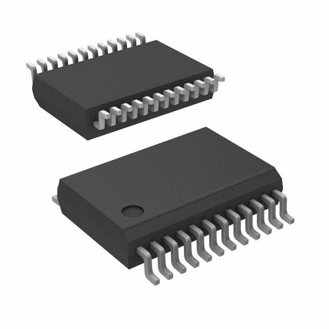
| 描述 | IC ADC 24-BIT SER PROGBL 24-SSOP模数转换器 - ADC 24-Bit Anlg-to-Dig Converter |
| 产品分类 | |
| 品牌 | Texas Instruments |
| 产品手册 | |
| 产品图片 |
|
| rohs | 符合RoHS无铅 / 符合限制有害物质指令(RoHS)规范要求 |
| 产品系列 | 数据转换器IC,模数转换器 - ADC,Texas Instruments ADS1240E- |
| 数据手册 | |
| 产品型号 | ADS1240E |
| PCN其它 | |
| 产品培训模块 | http://www.digikey.cn/PTM/IndividualPTM.page?site=cn&lang=zhs&ptm=13240 |
| 产品目录页面 | |
| 产品种类 | 模数转换器 - ADC |
| 位数 | 24 |
| 供应商器件封装 | 24-SSOP |
| 信噪比 | Yes |
| 其它名称 | 296-9301-5 |
| 分辨率 | 24 bit |
| 制造商产品页 | http://www.ti.com/general/docs/suppproductinfo.tsp?distId=10&orderablePartNumber=ADS1240E |
| 包装 | 管件 |
| 商标 | Texas Instruments |
| 安装类型 | 表面贴装 |
| 安装风格 | SMD/SMT |
| 封装 | Tube |
| 封装/外壳 | 24-SSOP(0.209",5.30mm 宽) |
| 封装/箱体 | SSOP-24 |
| 工作温度 | -40°C ~ 85°C |
| 工作电源电压 | 2.7 V to 5.25 V |
| 工厂包装数量 | 60 |
| 接口类型 | Serial SPI |
| 数据接口 | SPI |
| 最大功率耗散 | 1.9 mW |
| 最大工作温度 | + 85 C |
| 最小工作温度 | - 40 C |
| 标准包装 | 60 |
| 电压参考 | 0.1 V to 5 V |
| 电压源 | 模拟和数字 |
| 系列 | ADS1240 |
| 结构 | Sigma-Delta |
| 视频文件 | http://www.digikey.cn/classic/video.aspx?PlayerID=1364138032001&width=640&height=455&videoID=44659313001 |
| 转换器数 | 1 |
| 转换器数量 | 1 |
| 转换速率 | 15 S/s |
| 输入数和类型 | 4 个单端,单极2 个差分,单极 |
| 输入类型 | Differential |
| 通道数量 | 4 Channel |
| 采样率(每秒) | 15 |


- 商务部:美国ITC正式对集成电路等产品启动337调查
- 曝三星4nm工艺存在良率问题 高通将骁龙8 Gen1或转产台积电
- 太阳诱电将投资9.5亿元在常州建新厂生产MLCC 预计2023年完工
- 英特尔发布欧洲新工厂建设计划 深化IDM 2.0 战略
- 台积电先进制程称霸业界 有大客户加持明年业绩稳了
- 达到5530亿美元!SIA预计今年全球半导体销售额将创下新高
- 英特尔拟将自动驾驶子公司Mobileye上市 估值或超500亿美元
- 三星加码芯片和SET,合并消费电子和移动部门,撤换高东真等 CEO
- 三星电子宣布重大人事变动 还合并消费电子和移动部门
- 海关总署:前11个月进口集成电路产品价值2.52万亿元 增长14.8%


PDF Datasheet 数据手册内容提取
ADS1240 ADS1240 ADS1241 ADS1241 SBAS173C – JUNE 2001 – REVISED NOVEMBER 2003 24-Bit ANALOG-TO-DIGITAL CONVERTER FEATURES DESCRIPTION (cid:1) 24 BITS NO MISSING CODES The ADS1240 and ADS1241 are precision, wide dynamic range, (cid:1) SIMULTANEOUS 50Hz AND 60Hz REJECTION delta-sigma, Analog-to-Digital (A/D) converters with 24-bit resolution (–90dB MINIMUM) operating from 2.7V to 5.25V power supplies. The delta-sigma A/D (cid:1) 0.0015% INL converter provides up to 24 bits of no missing code performance and effective resolution of 21 bits. (cid:1) 21 BITS EFFECTIVE RESOLUTION (PGA = 1), 19 BITS (PGA = 128) The input channels are multiplexed. Internal buffering can be selected to provide very high input impedance for direct connection (cid:1) PGA GAINS FROM 1 TO 128 to transducers or low-level voltage signals. Burnout current sources (cid:1) SINGLE CYCLE SETTLING are provided that allow for detection of an open or shorted sensor. (cid:1) PROGRAMMABLE DATA OUTPUT RATES An 8-bit Digital-to-Analog (D/A) converter provides an offset cor- (cid:1) EXTERNAL DIFFERENTIAL REFERENCE rection with a range of 50% of the Full-Scale Range (FSR). OF 0.1V TO 5V The Programmable Gain Amplifier (PGA) provides selectable gains of (cid:1) ON-CHIP CALIBRATION 1 to 128, with an effective resolution of 19 bits at a gain of 128. The (cid:1) SPI™ COMPATIBLE A/D conversion is accomplished with a 2nd-order delta-sigma modu- lator and programmable Finite-Impulse Response (FIR) filter that (cid:1) 2.7V TO 5.25V SUPPLY RANGE provides a simultaneous 50Hz and 60Hz notch. The reference input (cid:1) 600µW POWER CONSUMPTION is differential and can be used for ratiometric conversion. (cid:1) UP TO EIGHT INPUT CHANNELS The serial interface is SPI compatible. Up to eight bits of data (cid:1) UP TO EIGHT DATA I/O I/O are also provided that can be used for input or output. The ADS1240 and ADS1241 are designed for high-resolution measure- ment applications in smart transmitters, industrial process control, APPLICATIONS weigh scales, chromatography, and portable instrumentation. (cid:1) INDUSTRIAL PROCESS CONTROL (cid:1) WEIGH SCALES AVDD AGND VREF+VREF– XIN XOUT (cid:1) LIQUID/GAS CHROMATOGRAPHY (cid:1) BLOOD ANALYSIS AVDD (cid:1) SMART TRANSMITTERS Clock Generator (cid:1) PORTABLE INSTRUMENTATION 2µA Offset DAC AIN0/D0 AIN1/D1 A = 1:128 AIN2/D2 AIN3/D3 MUX BUF + PGA 2Mnodd-uOlardtoerr DFiigltietarl Controller Registers AIN4/D4 AIN5/D5 AIN6/D6 AIN7/D7 POL AINCOM SCLK ADS1241 Serial Interface DIN Only 2µA DOUT CS AGND BUFEN DVDD DGND PDWN DSYNC RESET DRDY Please be aware that an important notice concerning availability, standard warranty, and use in critical applications of Texas Instruments semiconductor products and disclaimers thereto appears at the end of this data sheet. All trademarks property of their respective owners. PRODUCTION DATA information is current as of publication date. Copyright © 2001-2003, Texas Instruments Incorporated Products conform to specifications per the terms of Texas Instruments standard warranty. Production processing does not necessarily include testing of all parameters. www.ti.com
ABSOLUTE MAXIMUM RATINGS(1) ELECTROSTATIC AV to DGND......................................................................–0.3V to +6V DISCHARGE SENSITIVITY DD DV to DGND......................................................................–0.3V to +6V DD Input Current...............................................................100mA, Momentary This integrated circuit can be damaged by ESD. Texas Instru- DGND to AGND....................................................................–0.3V to 0.3V Input Current.................................................................10mA, Continuous ments recommends that all integrated circuits be handled with AIN.................................................................AGND –0.5V to AVDD + 0.5V appropriate precautions. Failure to observe proper handling Digital Input Voltage to DGND.................................–0.3V to DV + 0.3V DD and installation procedures can cause damage. Digital Output Voltage to DGND..............................–0.3V to DV + 0.3V DD Maximum Junction Temperature...................................................+150°C ESD damage can range from subtle performance degradation Operating Temperature Range.........................................–40°C to +85°C Storage Temperature Range..........................................–60°C to +150°C to complete device failure. Precision integrated circuits may be Lead Temperature (soldering, 10s) .............................................. +300°C more susceptible to damage because very small parametric changes could cause the device not to meet its published NOTE: (1) Stresses above these ratings may cause permanent damage. Exposure to absolute maximum conditions for extended periods may degrade specifications. device reliability. EVALUATION MODULE ORDERING INFORMATION PRODUCT DESCRIPTION ADS1241EVM ADS1240 and ADS1241 Evaluation Module PACKAGE/ORDERING INFORMATION SPECIFIED PACKAGE TEMPERATURE PACKAGE ORDERING TRANSPORT PRODUCT PACKAGE-LEAD DESIGNATOR(1) RANGE MARKING NUMBER MEDIA, QUANTITY ADS1240 SSOP-24 DB –40°C to +85°C ADS1240E ADS1240E Rails, 60 " " " " " ADS1240E/1K Tape and Reel, 1000 ADS1241 SSOP-28 DB –40°C to +85°C ADS1241E ADS1241E Rails, 48 " " " " " ADS1241E/1K Tape and Reel, 1000 NOTE: (1) For the most current specifications and package information, refer to our web site at www.ti.com. ° ° DIGITAL CHARACTERISTICS: –40 C to +85 C, DV 2.7V to 5.25V DD PARAMETER CONDITIONS MIN TYP MAX UNITS Digital Input/Output Logic Family CMOS Logic Level: V 0.8 • DV DV V IH DD DD V DGND 0.2 • DV V IL DD V I = 1mA DV – 0.4 V OH OH DD V I = 1mA DGND DGND + 0.4 V OL OL Input Leakage: I V = DV 10 µA IH I DD I V = 0 –10 µA IL I Master Clock Rate: f 1 5 MHz OSC Master Clock Period: t 1/f 200 1000 ns OSC OSC ADS1240, 1241 2 www.ti.com SBAS173C
ELECTRICAL CHARACTERISTICS: AV = 5V DD All specifications T to T , AV = +5V, DV = +2.7V to 5.25V, f = 19.2kHz, PGA = 1, Buffer ON, f = 15Hz, and V = +2.5V, unless otherwise specified. MIN MAX DD DD MOD DATA REF ADS1240 ADS1241 PARAMETER CONDITIONS MIN TYP MAX UNITS ANALOG INPUT (A 0 – A 7, A ) IN IN INCOM Analog Input Range Buffer OFF AGND – 0.1 AV + 0.1 V DD Buffer ON AGND + 0.05 AV – 1.5 V DD Full-Scale Input Range (In+) – (In–), See Block Diagram, RANGE = 0 ±V /PGA V REF RANGE = 1 ±V /(2 • PGA) V REF Differential Input Impedance Buffer OFF 5/PGA MΩ Buffer ON 5 GΩ Bandwidth f = 3.75Hz –3dB 1.65 Hz DATA f = 7.50Hz –3dB 3.44 Hz DATA f = 15.00Hz –3dB 14.6 Hz DATA Programmable Gain Amplifier User-Selectable Gain Ranges 1 128 Input Capacitance 9 pF Input Leakage Current Modulator OFF, T = 25°C 5 pA Burnout Current Sources 2 µA OFFSET DAC Offset DAC Range RANGE = 0 ±V /(2 • PGA) V REF RANGE = 1 ±V /(4 • PGA) V REF Offset Monotonicity 8 Bits Offset DAC Gain Error ±10 % Offset DAC Gain Error Drift 1 ppm/°C SYSTEM PERFORMANCE Resolution No Missing Codes 24 Bits Integral Nonlinearity End Point Fit ±0.0015 % of FS Offset Error(1) 7.5 ppm of FS Offset Drift(1) 0.02 ppm of FS/°C Gain Error 0.005 % Gain Error Drift(1) 0.5 ppm/°C Common-Mode Rejection at DC 100 dB f = 60Hz, f = 15Hz 130 dB CM DATA f = 50Hz, f = 15Hz 120 dB CM DATA Normal-Mode Rejection f = 50Hz, f = 15Hz 100 dB SIG DATA f = 60Hz, f = 15Hz 100 dB SIG DATA Output Noise See Typical Characteristics Power-Supply Rejection at DC, dB = –20 log(∆V /∆V )(2) 80 95 dB OUT DD VOLTAGE REFERENCE INPUT V V ≡ (REF IN+) – (REF IN–), RANGE = 0 0.1 2.5 2.6 V REF REF Reference Input Range REF IN+, REF IN– 0 AV V DD RANGE = 1 0.1 AV V DD Common-Mode Rejection at DC 120 dB Common-Mode Rejection f = 60Hz, f = 15Hz 120 dB VREFCM DATA Bias Current(3) V = 2.5V 1.3 µA REF POWER-SUPPLY REQUIREMENTS Power-Supply Voltage AV 4.75 5.25 V DD Analog Current PDWN = 0, or SLEEP 1 nA PGA = 1, Buffer OFF 120 250 µA PGA = 128, Buffer OFF 400 675 µA PGA = 1, Buffer ON 160 300 µA PGA = 128, Buffer ON 760 1275 µA Digital Current Normal Mode, DV = 5V 80 125 µA DD SLEEP Mode, DV = 5V 60 µA DD Read Data Continuous Mode, DV = 5V 230 µA DD PDWN 0.5 nA Power Dissipation PGA = 1, Buffer OFF, DV = 5V 1.1 1.9 mW DD NOTES: (1) Calibration can minimize these errors to the level of the noise. (2) ∆V is a change in digital result. OUT (3) 12pF switched capacitor at f clock frequency. SAMP ADS1240, 1241 3 SBAS173C www.ti.com
ELECTRICAL CHARACTERISTICS: AV = 3V DD All specifications –40°C to +85°C, AV = +3V, DV = +2.7V to 5.25V, f = 19.2kHz, PGA = 1, Buffer ON, f = 15Hz, and V = +1.25V, unless otherwise specified. DD DD MOD DATA REF ADS1240 ADS1241 PARAMETER CONDITIONS MIN TYP MAX UNITS ANALOG INPUT (A 0 – A 7, A ) IN IN INCOM Analog Input Range Buffer OFF AGND – 0.1 AV + 0.1 V DD Buffer ON AGND + 0.05 AV – 1.5 V DD Full-Scale Input Voltage Range (In+) – (In–) See Block Diagram, RANGE = 0 ±V /PGA V REF RANGE = 1 ±V /(2 • PGA) V REF Input Impedance Buffer OFF 5/PGA MΩ Differential Buffer ON 5 GΩ Bandwidth f = 3.75Hz –3dB 1.65 Hz DATA f = 7.50Hz –3dB 3.44 Hz DATA f = 15.00Hz –3dB 14.6 Hz DATA Programmable Gain Amplifier User-Selectable Gain Ranges 1 128 Input Capacitance 9 pF Input Leakage Current Modulator OFF, T = 25°C 5 pA Burnout Current Sources 2 µA OFFSET DAC Offset DAC Range RANGE = 0 ±V /(2 • PGA) V REF RANGE = 1 ±V /(4 • PGA) V REF Offset DAC Monotonicity 8 Bits Offset DAC Gain Error ±10 % Offset DAC Gain Error Drift 2 ppm/°C SYSTEM PERFORMANCE Resolution No Missing Codes 24 Bits Integral Nonlinearity End Point Fit ±0.0015 % of FS Offset Error(1) 15 ppm of FS Offset Drift(1) 0.04 ppm of FS/°C Gain Error 0.01 % Gain Error Drift(1) 1.0 ppm/°C Common-Mode Rejection at DC 100 dB f = 60Hz, f = 15Hz 130 dB CM DATA f = 50Hz, f = 15Hz 120 dB CM DATA Normal-Mode Rejection f = 50Hz, f = 15Hz 100 dB SIG DATA f = 60Hz, f = 15Hz 100 dB SIG DATA Output Noise See Typical Characteristics Power-Supply Rejection at DC, dB = –20 log(∆V /∆V )(2) 75 90 dB OUT DD VOLTAGE REFERENCE INPUT V V ≡ (REF IN+) – (REF IN–), RANGE = 0 0.1 1.25 1.30 V REF REF Reference Input Range REF IN+, REF IN– 0 AV V DD RANGE = 1 0.1 2.5 2.6 V Common-Mode Rejection at DC 120 dB Common-Mode Rejection f = 60Hz, f = 15Hz 120 dB VREFCM DATA Bias Current(3) V = 1.25 0.65 µA REF POWER-SUPPLY REQUIREMENTS Power-Supply Voltage AV 2.7 3.3 V DD Analog Current PDWN = 0, or SLEEP 1 nA PGA = 1, Buffer OFF 107 225 µA PGA = 128, Buffer OFF 355 600 µA PGA = 1, Buffer ON 118 275 µA PGA = 128, Buffer ON 483 1225 µA Digital Current Normal Mode, DV = 3V 50 100 µA DD SLEEP Mode, DV = 3V 40 µA DD Read Data Continuous Mode, DV = 3V 113 µA DD PDWN = 0 0.5 nA Power Dissipation PGA = 1, Buffer OFF, DV = 3V 0.6 1.2 mW DD NOTES: (1) Calibration can minimize these errors to the level of the noise. (2) ∆V is a change in digital result. OUT (3) 12pF switched capacitor at f clock frequency. SAMP ADS1240, 1241 4 www.ti.com SBAS173C
PIN CONFIGURATION (ADS1240) PIN CONFIGURATION (ADS1241) Top View SSOP Top View SSOP DV 1 28 BUFEN DD DVDD 1 24 BUFEN DGND 2 27 DRDY DGND 2 23 DRDY X 3 26 SCLK IN XIN 3 22 SCLK XOUT 4 25 DOUT XOUT 4 21 DOUT RESET 5 24 DIN RESET 5 20 DIN DSYNC 6 23 CS DSYNC 6 19 CS PDWN 7 22 POL ADS1240 ADS1241 PDWN 7 18 POL DGND 8 21 AV DD DGND 8 17 AVDD VREF+ 9 20 AGND VREF+ 9 16 AGND VREF– 10 19 AINCOM VREF– 10 15 AINCOM AIN0/D0 11 18 AIN3/D3 AIN0/D0 11 14 AIN3/D3 AIN1/D1 12 17 AIN2/D2 AIN1/D1 12 13 AIN2/D2 AIN4/D4 13 16 AIN7/D7 A 5/D5 14 15 A 6/D6 IN IN PIN DESCRIPTIONS (ADS1240) PIN DESCRIPTIONS (ADS1241) PIN PIN NUMBER NAME DESCRIPTION NUMBER NAME DESCRIPTION 1 DV Digital Power Supply 1 DV Digital Power Supply DD DD 2 DGND Digital Ground 2 DGND Digital Ground 3 X Clock Input IN 3 X Clock Input IN 4 X Clock Output, used with external crystals. OUT 4 XOUT Clock Output, used with external crystals. 5 RESET Active LOW, resets the entire device. 5 RESET Active LOW, resets the entire device. 6 DSYNC Active LOW, Synchronization Control 6 DSYNC Active LOW, Synchronization Control 7 PDWN Active LOW, Power Down. The power down func- tion shuts down the analog and digital circuits. 7 PDWN Active LOW, Power Down. The power down func- tion shuts down the analog and digital circuits. 8 DGND Digital Ground 9 V Positive Differential Reference Input 8 DGND Digital Ground REF+ 10 V Negative Differential Reference Input 9 V Positive Differential Reference Input REF– REF+ 11 A 0/D0 Analog Input 0 / Data I/O 0 IN 10 VREF– Negative Differential Reference Input 12 AIN1/D1 Analog Input 1 / Data I/O 1 11 AIN0/D0 Analog Input 0 / Data I/O 0 13 AIN4/D4 Analog Input 4 / Data I/O 4 12 AIN1/D1 Analog Input 1 / Data I/O 1 14 AIN5/D5 Analog Input 5 / Data I/O 5 13 AIN2/D2 Analog Input 2 / Data I/O 2 15 AIN6/D6 Analog Input 6 / Data I/O 6 16 A 7/D7 Analog Input 7 / Data I/O 7 14 A 3/D3 Analog Input 3 / Data I/O 3 IN IN 17 A 2/D2 Analog Input 2 / Data I/O 2 15 A Analog Input Common, connect to AGND if unused. IN INCOM 18 A 3/D3 Analog Input 3 / Data I/O 3 IN 16 AGND Analog Ground 19 A Analog Input Common, connect to AGND if unused. INCOM 17 AVDD Analog Power Supply 20 AGND Analog Ground 18 POL Serial Clock Polarity 21 AVDD Analog Power Supply 19 CS Active LOW, Chip Select 22 POL Serial Clock Polarity 23 CS Active LOW, Chip Select 20 D Serial Data Input, Schmitt Trigger IN 24 D Serial Data Input, Schmitt Trigger 21 D Serial Data Output IN OUT 25 D Serial Data Output 22 SCLK Serial Clock, Schmitt Trigger OUT 26 SCLK Serial Clock, Schmitt Trigger 23 DRDY Active LOW, Data Ready 27 DRDY Active LOW, Data Ready 24 BUFEN Buffer Enable 28 BUFEN Buffer Enable ADS1240, 1241 5 SBAS173C www.ti.com
TIMING DIAGRAMS CS t t t t 3 1 2 10 SCLK (POL = 0) SCLK (POL = 1) t4 t5 t6 t2 t11 DIN MSB LSB (Command or Command and Data) t7 t8 t9 DOUT MSB(1) LSB(1) NOTE: (1) Bit order = 0. SCLK Reset Waveform ADS1240 or ADS1241 Resets On Falling Edge 300 • t < t < 500 • t OSC 12 OSC t13 t13 t13 : > 5 • tOSC SCLK 550 • tOSC < t14 < 750 • tOSC 1050 • t < t < 1250 • t t t t OSC 15 OSC 12 14 15 DIAGRAM 1. t t 16 DATA DRDY RESET, DSYNC, PDWN t t 17 18 SCLK t 19 DIAGRAM 2. TIMING CHARACTERISTICS TABLES SPEC DESCRIPTION MIN MAX UNITS t SCLK Period 4 t Periods 1 OSC 3 DRDY Periods t SCLK Pulse Width, HIGH and LOW 200 ns 2 t CS low to first SCLK Edge; Setup Time(2) 0 ns 3 t D Valid to SCLK Edge; Setup Time 50 ns 4 IN t Valid D to SCLK Edge; Hold Time 50 ns 5 IN t Delay between last SCLK edge for D and first SCLK edge for D : 6 IN OUT RDATA, RDATAC, RREG, WREG 50 t Periods OSC t (1) SCLK Edge to Valid New D 50 ns 7 OUT t (1) SCLK Edge to D , Hold Time 0 ns 8 OUT t Last SCLK Edge to D Tri-State 6 10 t Periods 9 OUT OSC NOTE: D goes tri-state immediately when CS goes HIGH. OUT t CS LOW time after final SCLK edge. 0 ns 10 t Final SCLK edge of one command until first edge SCLK 11 of next command: RREG, WREG, DSYNC, SLEEP, RDATA, RDATAC, STOPC 4 t Periods OSC SELFGCAL, SELFOCAL, SYSOCAL, SYSGCAL 2 DRDY Periods SELFCAL 4 DRDY Periods RESET (also SCLK Reset or RESET Pin) 16 t Periods OSC t Pulse Width 4 t Periods 16 OSC t Allowed analog input change for next valid conversion. 5000 t Periods 17 OSC t DOR update, DOR data not valid. 4 t Periods 18 OSC t First SCLK after DRDY goes LOW: 19 RDATAC Mode 10 t Periods OSC Any other mode 0 t Periods OSC NOTES: (1) Load = 20pF10kΩ to DGND. (2) CS may be tied LOW. ADS1240, 1241 6 www.ti.com SBAS173C
TYPICAL CHARACTERISTICS All specifications, AV = +5V, DV = +5V, f = 2.4576MHz, PGA = 1, f = 15Hz, and V ≡ (REF IN+) – (REF IN–) = +2.5V, unless otherwise specified. DD DD OSC DATA REF EFFECTIVE NUMBER OF BITS vs PGA SETTING EFFECTIVE NUMBER OF BITS vs PGA SETTING 21.5 22 DR = 10 21.0 21 20.5 DR = 10 DR = 01 20 20.0 B (rms) 19.5 B (rms) 19 DR = 01 O 19.0 O 18 EN 18.5 DR = 00 EN DR = 00 17 18.0 Buffer ON Buffer OFF 16 17.5 17.0 15 1 2 4 8 16 32 64 128 1 2 4 8 16 32 64 128 PGA Setting PGA Setting EFFECTIVE NUMBER OF BITS vs PGA SETTING NOISE vs INPUT SIGNAL 20.5 2.0 20.0 1.8 DR = 10 1.6 19.5 S) F 1.4 ms) 19.0 DR = 01 m of 1.2 ENOB (r 111887...505 DR = 00 se (rms, pp 100...086 oi 17.0 N 0.4 Buffer OFF, V = 1.25V REF 16.5 0.2 16.0 0 1 2 4 8 16 32 64 128 –2.5 –1.5 –0.5 0.5 1.5 2.5 PGA Setting VIN (V) COMMON-MODE REJECTION RATIO POWER SUPPLY REJECTION RATIO vs FREQUENCY vs FREQUENCY 140 140 120 120 100 100 R (dB) 80 R (dB) 80 MR 60 SR 60 C P 40 40 20 20 Buffer ON Buffer ON 0 0 1 10 100 1k 10k 100k 1 10 100 1k 10k 100k Frequency of Power Supply (Hz) Frequency of Power Supply (Hz) ADS1240, 1241 7 SBAS173C www.ti.com
TYPICAL CHARACTERISTICS (Cont.) All specifications, AV = +5V, DV = +5V, f = 2.4576MHz, PGA = 1, f = 15Hz, and V ≡ (REF IN+) – (REF IN–) = +2.5V, unless otherwise specified. DD DD OSC DATA REF OFFSET vs TEMPERATURE GAIN vs TEMPERATURE (Cal at 25°C) (Cal at 25°C) 50 1.00010 PGA1 PGA16 1.00006 0 m of FS) –50 malized) 1.00002 Offset (pp –100 PGA64 Gain (Nor 00..9999999984 PGA128 –150 0.99990 –200 0.99986 –50 –30 –10 10 30 50 70 90 –50 –30 –10 10 30 50 70 90 Temperature (°C) Temperature (°C) INTEGRAL NONLINEARITY vs INPUT SIGNAL ANALOG CURRENT vs TEMPERATURE 10 150 8 140 –40°C AVDD = 5 6 130 4 120 S) +85°C m of F 20 µnt (A) 111000 p e AV = 3 L (p –2 Curr 90 DD N I –4 80 +25°C –6 70 Buffer OFF –8 60 –10 50 –2.5 –2.0 –1.5 –1.0 –0.5 0 0.5 1.0 1.5 2.0 2.5 –50 –30 –10 10 30 50 70 90 V (V) Temperature (°C) IN ANALOG CURRENT vs PGA DIGITAL CURRENT vs SUPPLY 900 300 AV = 5V, Buffer = ON DD 800 Buffer = OFF 250 700 600 200 A) A) SLEEP Normal Normal µ (OG 500 AVDD = 3V, Buffer = ON µ (AL 150 4.91MHz 4.91MHz 2.45MHz ANAL 400 Buffer = OFF DIGIT I 300 I 100 200 50 100 SLEEP Power Down 2.45MHz 0 0 1 2 4 8 16 32 64 128 3.0 3.5 4.0 4.5 5.0 PGA Setting V (V) DD ADS1240, 1241 8 www.ti.com SBAS173C
TYPICAL CHARACTERISTICS (Cont.) All specifications, AV = +5V, DV = +5V, f = 2.4576MHz, PGA = 1, f = 15Hz, and V ≡ (REF IN+) – (REF IN–) = +2.5V, unless otherwise specified. DD DD OSC DATA REF OFFSET DAC OFFSET vs TEMPERATURE NOISE HISTOGRAM (Cal at 25°C) 3500 200 10k Readings V = 0V 170 3000 IN 140 s ce 2500 R) 110 Occurren 2000 pm of FS 8500 mber of 11500000 Offset (p –2100 Nu –40 500 –70 –100 0 –50 –30 –10 10 30 50 70 90 –3.5–3.0–2.5–2.0–1.5 –1 –0.5 0 0.5 1.0 1.5 2.0 2.5 3.0 3.5 Temperature (°C) ppm of FS OFFSET DAC GAIN vs TEMPERATURE OFFSET DAC (Cal at 25°C) NOISE vs SETTING 1.00020 0.8 1.00016 0.7 1.00012 1.00008 S) 0.6 ain (Normalized) 1100....00990099009900994062 e (rms, ppm of F 000...543 G 0.99988 Nois 0.2 0.99984 0.99980 0.1 0.99976 0 –50 –30 –10 10 30 50 70 90 –128 –96 –64 –32 0 32 64 96 128 Temperature (°C) Offset DAC Setting ADS1240, 1241 9 SBAS173C www.ti.com
OVERVIEW channel. With this method, it is possible to have up to eight single-ended input channels or four independent differential INPUT MULTIPLEXER input channels for the ADS1241, and four single-ended input The input multiplexer provides for any combination of differ- channels or two independent differential input channels for ential inputs to be selected on any of the input channels, as the ADS1240. Note that AINCOM can be treated as an input shown in Figure 1. For example, if A 0 is selected as the channel. IN positive differential input channel, any other channel can be The ADS1240 and ADS1241 feature a single-cycle settling selected as the negative terminal for the differential input digital filter that provides valid data on the first conversion after a new channel selection. In order to minimize the settling error, synchronize MUX changes to the conversion beginning, which is indicated by the falling edge of DRDY. In other words, issuing a MUX change through the WREG AIN0/D0 command immediately after DRDY goes LOW minimizes the settling error. Increasing the time between the conversion AIN1/D1 AVDD beginning (DRDY goes LOW) and the MUX change com- mand (t ) results in a settling error in the conversion DELAY AIN2/D2 Burnout Current Source data, as shown in Figure 2. BURNOUT CURRENT SOURCES AIN3/D3 The Burnout Current Sources can be used to detect sensor Input short-circuit or open-circuit conditions. Setting the Burnout AIN4/D4 Buffer Current Sources (BOCS) bit in the SETUP register activates two 2µA current sources called burnout current sources. One AIN5/D5 of the current sources is connected to the converter’s nega- tive input and the other is connected to the converter’s Burnout Current Source AIN6/D6 positive input. AGND Figure 3 shows the situation for an open-circuit sensor. This is a potential failure mode for many kinds of remotely con- AIN7/D7 nected sensors. The current source on the positive input acts as a pull-up, causing the positive input to go to the positive ADS1241 AINCOM analog supply, and the current source on the negative input Only acts as a pull-down, causing the negative input to go to ground. The ADS1240/41 therefore outputs full-scale (7FFFFF FIGURE 1. Input Multiplexer Configuration. Hex). New Conversion Begins, Previous Conversion Data Complete Previous Conversion New Conversion Complete DRDY tDELAY SCLK (POL = 0) DIN MSB LSB SETTLING ERROR vs DELAY TIME fCLK = 2.4576MHz 10.000000 1.000000 %) 0.100000 Error ( 0.010000 Settling 00..000010010000 0.000010 0.000001 0 2 4 6 8 10 12 14 16 Delay Time, tDELAY (ms) FIGURE 2. Input Multiplexer Configuration. ADS1240, 1241 10 www.ti.com SBAS173C
The buffer draws additional current when activated. The current required by the buffer depends on the PGA setting. AV DD When the PGA is set to 1, the buffer uses approximately 50µA; when the PGA is set to 128, the buffer uses approxi- 2µA mately 500µA. AV DD PGA OPEN CIRCUIT ADC CODE = 0x7FFFFF H The Programmable Gain Amplifier (PGA) can be set to gains 0V of 1, 2, 4, 8, 16, 32, 64, or 128. Using the PGA can improve the effective resolution of the A/D converter. For instance, with a 2µA PGA of 1 on a 5V full-scale signal, the A/D converter can resolve down to 1µV. With a PGA of 128 and a full-scale signal of 39mV, the A/D converter can resolve down to 75nV. AV DD current increases with PGA settings higher than 4. FIGURE 3. Burnout detection while sensor is open-circuited. OFFSET DAC Figure 4 shows a short-circuited sensor. Since the inputs are The input to the PGA can be shifted by half the full-scale input shorted and at the same potential, the ADS1240/41 signal range of the PGA using the Offset DAC (ODAC) register. The outputs are approximately zero. (Note that the code for ODAC register is an 8-bit value; the MSB is the sign and the shorted inputs is not exactly zero due to internal series seven LSBs provide the magnitude of the offset. Using the resistance, low-level noise and other error sources.) offset DAC does not reduce the performance of the A/D converter. For more details on the ODAC, please refer to TI application report SBAA077. AV DD MODULATOR 2µA The modulator is a single-loop second-order system. The modulator runs at a clock speed (f ) that is derived from MOD AV /2 DD the external clock (f ). The frequency division is deter- OSC SHORT mined by the SPEED bit in the SETUP register, as shown in ADC CODE ≅ 0 CIRCUIT Table I. AV /2 DD 2µA SPEED DR BITS 1st NOTCH f BIT f 00 01 10 FREQ. OSC MOD 2.4576MHz 0 19,200Hz 15Hz 7.5Hz 3.75Hz 50/60Hz 1 9,600Hz 7.5Hz 3.75Hz 1.875Hz 25/30Hz 4.9152MHz 0 38,400Hz 30Hz 15Hz 7.5Hz 100/120Hz 1 19,200Hz 15Hz 7.5Hz 3.75Hz 50/60Hz FIGURE 4. Burnout detection while sensor is short-circuited. TABLE I. Output Configuration. INPUT BUFFER CALIBRATION The input impedance of the ADS1240/41 without the buffer enabled is approximately 5MΩ/PGA. For systems requiring The offset and gain errors can be minimized with calibration. very high input impedance, the ADS1240/41 provides a The ADS1240 and ADS1241 support both self and system chopper-stabilized differential FET-input voltage buffer. When calibration. activated, the buffer raises the ADS1240/41 input impedance Self-calibration of the ADS1240 and ADS1241 corrects inter- to approximately 5GΩ. nal offset and gain errors and is handled by three commands: The buffer’s input range is approximately 50mV to AV – SELFCAL, SELFGAL, and SLEFOCAL. The SELFCAL com- DD 1.5V. The buffer’s linearity will degrade beyond this range. mand performs both an offset and gain calibration. SELFGCAL Differential signals should be adjusted so that both signals performs a gain calibration and SELFOCAL performs an are within the buffer’s input range. offset calibration, each of which takes two tDATA periods to complete. During self-calibration, the ADC inputs are discon- The buffer can be enabled using the BUFEN pin or the nected internally from the input pins. The PGA must be set to BUFEN bit in the ACR register. The buffer is on when the 1 prior to issuing a SELFCAL or SELFGCAL command. Any BUFEN pin is high and the BUFEN bit is set to one. If the PGA is allowed when issuing a SELFOCAL command. For BUFEN pin is low, the buffer is disabled. If the BUFEN bit is example, if using PGA = 64, first set PGA = 1 and issue set to zero, the buffer is also disabled. ADS1240, 1241 11 SBAS173C www.ti.com
SELFGCAL. Afterwards set PGA = 64 and issue SELFOCAL. For operation with a reference voltage greater than (AV – DD X 1.5) volts, the buffer must also be turned off during gain self- C IN 1 calibration to avoid exceeding the buffer input range. Crystal System calibration corrects both internal and external offset X OUT and gain errors. While performing system calibration, the C2 appropriate signal must be applied to the inputs. The system offset calibration command (SYSOCAL) requires a zero input differential signal (see Table IV, page 18). It then computes FIGURE 5. Crystal Connection. the offset that nullifies the offset in the system. The system gain calibration command (SYSGCAL) requires a positive full-scale input signal. It then computes a value to nullify the CLOCK PART gain error in the system. Each of these calibrations takes two SOURCE FREQUENCY C C NUMBER 1 2 tDATA periods to complete. System gain calibration is recom- Crystal 2.4576 0-20pF 0-20pF ECS, ECSD 2.45 - 32 mended for the best gain calibration at higher PGAs. Crystal 4.9152 0-20pF 0-20pF ECS, ECSL 4.91 Crystal 4.9152 0-20pF 0-20pF ECS, ECSD 4.91 Calibration should be performed after power on, a change in Crystal 4.9152 0-20pF 0-20pF CTS, MP 042 4M9182 temperature, or a change of the PGA. The RANGE bit (ACR bit 2) must be zero during calibration. TABLE II. Recommended Crystals. Calibration removes the effects of the ODAC; therefore, dis- able the ODAC during calibration, and enable again after DIGITAL FILTER calibration is complete. The ADS1240 and ADS1241 have a 1279 tap linear phase At the completion of calibration, the DRDY signal goes low, Finite Impulse Response (FIR) digital filter that a user can indicating the calibration is finished. The first data after configure for various output data rates. When a 2.4576MHz calibration should be discarded since it may be corrupt from crystal is used, the device can be programmed for an output calibration data remaining in the filter. The second data is data rate of 15Hz, 7.5Hz, or 3.75Hz. Under these conditions, always valid. the digital filter rejects both 50Hz and 60Hz interference. Figure 6 shows the digital filter frequency response for data output rates of 15Hz, 7.5Hz, and 3.75Hz. EXTERNAL VOLTAGE REFERENCE If a different data output rate is desired, a different crystal The ADS1240 and ADS1241 require an external voltage frequency can be used. However, the rejection frequencies reference. The selection for the voltage reference value is shift accordingly. For example, a 3.6864MHz master clock with made through the ACR register. the default register condition has: The external voltage reference is differential and is repre- (3.6864MHz/2.4576MHz) • 15Hz = 22.5Hz data output rate sented by the voltage difference between the pins: +V REF and –V . The absolute voltage on either pin, +V or and the first and second notch is: REF REF –V can range from AGND to AV . However, the follow- REF, DD 1.5 • (50Hz and 60Hz) = 75Hz and 90Hz ing limitations apply: For AV = 5.0V and RANGE = 0 in the ACR, the differential DD DATA I/O INTERFACE V must not exceed 2.5V. REF The ADS1240 has four pins and the ADS1241 has eight pins For AV = 5.0V and RANGE = 1 in the ACR, the differential DD that serve a dual purpose as both analog inputs and data V must not exceed 5V. REF I/O. These pins are powered from AV and are configured DD For AV = 3.0V and RANGE = 0 in the ACR, the differential through the IOCON, DIR, and DIO registers. These pins DD V must not exceed 1.25V. can be individually configured as either analog inputs or data REF I/O. See Figure 7 (page 14) for the equivalent schematic of For AV = 3.0V and RANGE = 1 in the ACR, the differential DD an Analog/Data I/O pin. V must not exceed 2.5V. REF The IOCON register defines the pin as either an analog input or data I/O. The power-up state is an analog input. If the pin CLOCK GENERATOR is configured as an analog input in the IOCON register, the The clock source for the ADS1240 and ADS1241 can be DIR and DIO registers have no effect on the state of the pin. provided from a crystal, oscillator, or external clock. When the If the pin is configured as data I/O in the IOCON register, clock source is a crystal, external capacitors must be provided then DIR and DIO are used to control the state of the pin. to ensure start-up and stable clock frequency. This is shown in The DIR register controls the direction of the data pin, either both Figure 5 and Table II. X is only for use with external OUT as an input or output. If the pin is configured as an input in crystals and it should not be used as a clock driver for external the DIR register, then the corresponding DIO register bit circuitry. reflects the state of the pin. Make sure the pin is driven to a ADS1240, 1241 12 www.ti.com SBAS173C
ADS1240 AND ADS1241 FREQUENCY RESPONSE FROM 45Hz to 65Hz FILTER RESPONSE WHEN f = 15Hz WHEN f = 15Hz DATA DATA 0 –40 –20 –50 –40 –60 –70 –60 B) dB) –80 e (d –80 Gain ( –100 gnitud –1–0900 –120 Ma –110 –140 –120 –160 –130 –180 –140 0 20 40 60 80 100 120 140 160 180 200 45 50 55 60 65 Frequency (Hz) Frequency (Hz) ADS1240 AND ADS1241 FREQUENCY RESPONSE FROM 45Hz to 65Hz FILTER RESPONSE WHEN f = 7.5Hz WHEN f = 7.5Hz DATA DATA 0 –40 –20 –50 –40 –60 –70 –60 B) Gain (dB) –1–0800 gnitude (d –1––089000 –120 Ma –110 –140 –120 –160 –130 –180 –140 0 20 40 60 80 100 120 140 160 180 200 45 50 55 60 65 Frequency (Hz) Frequency (Hz) ADS1240 AND ADS1241 FREQUENCY RESPONSE FROM 45Hz to 65Hz FILTER RESPONSE WHEN fDATA = 3.75Hz WHEN fDATA = 3.75Hz 0 –40 –20 –50 –40 –60 –70 –60 B) dB) –80 e (d –80 Gain ( –100 gnitud –1–0900 –120 Ma –110 –140 –120 –160 –130 –180 –140 0 20 40 60 80 100 120 140 160 180 200 45 50 55 60 65 Frequency (Hz) Frequency (Hz) f = 2.4576MHz, SPEED = 0 or f = 4.9152MHz, SPEED = 1 OSC OSC ATTENUATION DATA –3dB OUTPUT RATE BANDWIDTH f = 50 ± 0.3Hz f = 60 ± 0.3Hz f = 50 ± 1Hz f = 60 ± 1Hz IN IN IN IN 15Hz 14.6Hz –80.8dB –87.3dB –68.5dB –76.1dB 7.5Hz 3.44Hz –85.9dB –87.4dB –71.5dB –76.2dB 3.75Hz 1.65Hz –93.8dB –88.6dB –86.8dB –77.3dB FIGURE 6. Filter Frequency Responses. ADS1240, 1241 13 SBAS173C www.ti.com
logic one or zero when configured as an input to prevent Data Continuous Mode (RDATAC) command should not be excess current dissipation. If the pin is configured as an issued when D and D are connected. While in RDATAC IN OUT output in the DIR register, then the corresponding DIO mode, D looks for the STOPC or RESET command. If IN register bit value determines the state of the output pin either of these 8-bit bytes appear on D (which is con- OUT (0 = AGND, 1 = AV ). nected to D ), the RDATAC mode ends. DD IN It is still possible to perform A/D conversions on a pin configured as data I/O. This may be useful as a test mode, DATA READY DRDY PIN where the data I/O pin is driven and an A/D conversion is The DRDY line is used as a status signal to indicate when done on the pin. data is ready to be read from the internal data register. DRDY goes LOW when a new data word is available in the DOR register. It is reset HIGH when a read operation from IOCON the data register is complete. It also goes HIGH prior to the DIR updating of the output register to indicate when not to read from the device to ensure that a data read is not attempted while the register is being updated. DIO WRITE A x/Dx The status of DRDY can also be obtained by interrogating bit IN To Analog Mux 7 of the ACR register (address 2 ). The serial interface can H DIO READ operate in 3-wire mode by tying the CS input LOW. In this case, the SCLK, D , and D lines are used to communi- IN OUT cate with the ADS1240 and ADS1241. This scheme is FIGURE 7. Analog/Data Interface Pin. suitable for interfacing to microcontrollers. If CS is required as a decoding signal, it can be generated from a port bit of SERIAL PERIPHERAL INTERFACE the microcontroller. The Serial Peripheral Interface (SPI) allows a controller to communicate synchronously with the ADS1240 and ADS1241. DSYNC OPERATION The ADS1240 and ADS1241 operate in slave-only mode. Synchronization can be achieved either through the DSYNC The serial interface is a standard four-wire SPI (CS, SCLK, pin or the DSYNC command. When the DSYNC pin is used, D and D ) interface that supports both serial clock IN OUT the digital circuitry is reset on the falling edge of DSYNC. polarities (POL pin). While DSYNC is LOW, the serial interface is deactivated. Chip Select (CS) Reset is released when DSYNC is taken HIGH. Synchroni- The chip select (CS) input must be externally asserted zation occurs on the next rising edge of the system clock before communicating with the ADS1240 or ADS1241. CS after DSYNC is taken HIGH. must stay LOW for the duration of the communication. When the DSYNC command is sent, the digital filter is reset Whenever CS goes HIGH, the serial interface is reset. CS on the edge of the last SCLK of the DSYNC command. The may be hard-wired LOW. modulator is held in RESET until the next edge of SCLK is Serial Clock (SCLK) detected. Synchronization occurs on the next rising edge of the system clock after the first SCLK following the DSYNC The serial clock (SCLK) features a Schmitt-triggered input command. and is used to clock D and D data. Make sure to have IN OUT a clean SCLK to prevent accidental double-shifting of the data. If SCLK is not toggled within 3 DRDY pulses, the serial POWER-UP—SUPPLY VOLTAGE RAMP RATE interface resets on the next SCLK pulse and starts a new The power-on reset circuitry was designed to accommodate communication cycle. A special pattern on SCLK resets the digital supply ramp rates as slow as 1V/10ms. To ensure entire chip; see the RESET section for additional information. proper operation, the power supply should ramp monotoni- Clock Polarity (POL) cally. The clock polarity input (POL) controls the polarity of SCLK. When POL is LOW, data is clocked on the falling edge of RESET SCLK and SCLK should be idled LOW. Likewise, when POL The user can reset the registers to their default values in is HIGH, the data is clocked on the rising edge of SCLK and three different ways: by asserting the RESET pin; by issuing SCLK should be idled HIGH. the RESET command; or by applying a special waveform on the SCLK (the SCLK Reset Waveform, as shown in the Data Input (D ) and Data Output (D ) IN OUT Timing Diagram). Note: if both POL and SCLK pins are held The data input (D ) and data output (D ) receive and send IN OUT high, applying the SCLK Reset Waveform to the CS pin also data from the ADS1240 and ADS1241. D is high imped- OUT resets the part. ance when not in use to allow D and D to be connected IN OUT together and driven by a bidirectional bus. Note: the Read ADS1240, 1241 14 www.ti.com SBAS173C
ADS1240 AND ADS1241 tion needed to configure the part, such as data format, multiplexer settings, calibration settings, data rate, etc. The REGISTER set of the 16 registers are shown in Table III. The operation of the device is set up through individual registers. Collectively, the registers contain all the informa- ADDRESS REGISTER BIT 7 BIT 6 BIT 5 BIT 4 BIT 3 BIT 2 BIT 1 BIT 0 00 SETUP ID ID ID ID BOCS PGA2 PGA1 PGA0 H 01 MUX PSEL3 PSEL2 PSEL1 PSEL0 NSEL3 NSEL2 NSEL1 NSEL0 H 02 ACR DRDY U/B SPEED BUFEN BIT ORDER RANGE DR1 DR0 H 03 ODAC SIGN OSET6 OSET5 OSET4 OSET3 OSET2 OSET1 OSET0 H 04 DIO DIO_7 DIO_6 DIO_5 DIO_4 DIO_3 DIO_2 DIO_1 DIO_0 H 05 DIR DIR_7 DIR_6 DIR_5 DIR_4 DIR_3 DIR_2 DIR_1 DIR_0 H 06 IOCON IO7 IO6 IO5 IO4 IO3 IO2 IO1 IO0 H 07 OCR0 OCR07 OCR06 OCR05 OCR04 OCR03 OCR02 OCR01 OCR00 H 08 OCR1 OCR15 OCR14 OCR13 OCR12 OCR11 OCR10 OCR09 OCR08 H 09 OCR2 OCR23 OCR22 OCR21 OCR20 OCR19 OCR18 OCR17 OCR16 H 0A FSR0 FSR07 FSR06 FSR05 FSR04 FSR03 FSR02 FSR01 FSR00 H 0B FSR1 FSR15 FSR14 FSR13 FSR12 FSR11 FSR10 FSR09 FSR08 H 0C FSR2 FSR23 FSR22 FSR21 FSR20 FSR19 FSR18 FSR17 FSR16 H 0D DOR2 DOR23 DOR22 DOR21 DOR20 DOR19 DOR18 DOR17 DOR16 H 0E DOR1 DOR15 DOR14 DOR13 DOR12 DOR11 DOR10 DOR09 DOR08 H 0F DOR0 DOR07 DOR16 FSR21 DOR04 DOR03 DOR02 DOR01 DOR00 H TABLE III. Registers. DETAILED REGISTER DEFINITIONS MUX (Address 01 ) Multiplexer Control Register H SETUP (Address 00 ) Setup Register Reset Value = 01 H H Reset Value = iiii0000 bit 7 bit 6 bit 5 bit 4 bit 3 bit 2 bit 1 bit 0 bit 7 bit 6 bit 5 bit 4 bit 3 bit 2 bit 1 bit 0 PSEL3 PSEL2 PSEL1 PSEL0 NSEL3 NSEL2 NSEL1 NSEL0 ID ID ID ID BOCS PGA2 PGA1 PGA0 bit 7-4 PSEL3: PSEL2: PSEL1: PSEL0: Positive Channel bit 7-4 Factory Programmed Bits Select bit 3 BOCS: Burnout Current Source 0000 = AIN0 (default) 0 = Disabled (default) 0001 = AIN1 1 = Enabled 0010 = AIN2 0011 = A 3 bit 2-0 PGA2: PGA1: PGA0: Programmable Gain Amplifier IN 0100 = A 4 Gain Selection IN 0101 = A 5 000 = 1 (default) IN 0110 = A 6 001 = 2 IN 0111 = A 7 010 = 4 IN 1xxx = AINCOM (except when xxx = 111) 011 = 8 1111 = Reserved 100 = 16 101 = 32 bit 3-0 NSEL3: NSEL2: NSEL1: NSEL0: Negative Channel 110 = 64 Select 111 = 128 0000 = AIN0 0001 = A 1 (default) IN 0010 = A 2 IN 0011 = A 3 IN 0100 = A 4 IN 0101 = A 5 IN 0110 = A 6 IN 0111 = A 7 IN 1xxx = AINCOM (except when xxx = 111) 1111 = Reserved ADS1240, 1241 15 SBAS173C www.ti.com
ACR (Address 02 ) Analog Control Register ODAC (Address 03 ) Offset DAC H Reset Value = X0 Reset Value = 00 H H bit 7 bit 6 bit 5 bit 4 bit 3 bit 2 bit 1 bit 0 bit 7 bit 6 bit 5 bit 4 bit 3 bit 2 bit 1 bit 0 DRDY U/B SPEED BUFEN BIT ORDER RANGE DR1 DR0 SIGN OSET6 OSET5 OSET4 OSET3 OSET2 OSET1 OSET0 bit 7 DRDY: Data Ready (Read Only) bit 7 Sign This bit duplicates the state of the DRDY pin. 0 = Positive bit 6 U/B: Data Format 1 = Negative 0 = Bipolar (default) 1 = Unipolar Offset= VREF •OSET[6:0] RANGE=0 2•PGA 127 U/B ANALOG INPUT DIGITAL OUTPUT (Hex) +FSR 0x7FFFFF V OSET[6:0] 0 Zero 0x000000 Offset= REF • RANGE=1 –FSR 0x800000 4•PGA 127 +FSR 0xFFFFFF 1 Zero 0x000000 NOTE: The offset DAC must be enabled after calibration or the calibration –FSR 0x000000 nullifies the effects. bit 5 SPEED: Modulator Clock Speed DIO (Address 04 ) Data I/O 0 = f = f /128 (default) H MOD OSC Reset Value = 00 1 = f = f /256 H MOD OSC bit 7 bit 6 bit 5 bit 4 bit 3 bit 2 bit 1 bit 0 bit 4 BUFEN: Buffer Enable 0 = Buffer Disabled (default) DIO 7 DIO 6 DIO 5 DIO 4 DIO 3 DIO 2 DIO 1 DIO 0 1 = Buffer Enabled If the IOCON register is configured for data, a value written bit 3 BIT ORDER: Data Output Bit Order to this register appears on the data I/O pins if the pin is 0 = Most Significant Bit Transmitted First (default) configured as an output in the DIR register. Reading this 1 = Least Significant Bit Transmitted First register returns the value of the data I/O pins. This configuration bit controls only the bit order Bit 4 to bit 7 is not used in ADS1240. within the byte of data that is shifted out. Data is always shifted out of the part most significant byte DIR (Address 05 ) Direction Control for Data I/O H first. Data is always shifted into the part most Reset Value = FF H significant bit first. bit 7 bit 6 bit 5 bit 4 bit 3 bit 2 bit 1 bit 0 bit 2 RANGE: Range Select DIR7 DIR6 DIR5 DIR4 DIR3 DIR2 DIR1 DIR0 0 = Full-Scale Input Range equal to ±V REF (default). Each bit controls whether the corresponding data I/O pin is 1 = Full-Scale Input Range equal to ±1/2 V an output (= 0) or input (= 1). The default power-up state is REF NOTE: This allows reference voltages as high as as inputs. AV , but even with a 5V reference voltage the Bit 4 to bit 7 is not used in ADS1240. DD calibration must be performed with this bit set to 0. bit 1-0 DR1: DR0: Data Rate IOCON (Address 06 ) I/O Configuration Register H (f = 2.4576MHz, SPEED = 0) Reset Value = 00 OSC H 00 = 15Hz (default) bit 7 bit 6 bit 5 bit 4 bit 3 bit 2 bit 1 bit 0 01 = 7.5Hz IO7 IO6 IO5 IO4 IO3 IO2 IO1 IO0 10 = 3.75Hz 11 = Reserved bit 7-0 IO7: IO0: Data I/O Configuration 0 =Analog (default) 1 =Data Configuring the pin as a data I/O pin allows it to be controlled through the DIO and DIR registers. Bit 4 to bit 7 is not used in ADS1240. OCR0 (Address 07 ) Offset Calibration Coefficient H (Least Significant Byte) Reset Value = 00 H bit 7 bit 6 bit 5 bit 4 bit 3 bit 2 bit 1 bit 0 OCR07 OCR06 OCR05 OCR04 OCR03 OCR02 OCR01 OCR00 ADS1240, 1241 16 www.ti.com SBAS173C
OCR1 (Address 08 ) Offset Calibration Coefficient FSR2 (Address 0C ) Full-Scale Register H H (Middle Byte) (Most Significant Byte) Reset Value = 00 Reset Value = 55 H H bit 7 bit 6 bit 5 bit 4 bit 3 bit 2 bit 1 bit 0 bit 7 bit 6 bit 5 bit 4 bit 3 bit 2 bit 1 bit 0 OCR15 OCR14 OCR13 OCR12 OCR11 OCR10 OCR09 OCR08 FSR23 FSR22 FSR21 FSR20 FSR19 FSR18 FSR17 FSR16 OCR2 (Address 09 ) Offset Calibration Coefficient DOR2 (Address 0D ) Data Output Register H H (Most Significant Byte) (Most Significant Byte) (Read Only) Reset Value = 00 Reset Value = 00 H H bit 7 bit 6 bit 5 bit 4 bit 3 bit 2 bit 1 bit 0 bit 7 bit 6 bit 5 bit 4 bit 3 bit 2 bit 1 bit 0 OCR23 OCR22 OCR21 OCR20 OCR19 OCR18 OCR17 OCR16 DOR23 DOR22 DOR21 DOR20 DOR19 DOR18 DOR17 DOR16 FSR0 (Address 0A ) Full-Scale Register DOR1 (Address 0E ) Data Output Register H H (Least Significant Byte) (Middle Byte) (Read Only) Reset Value = 59 Reset Value = 00 H H bit 7 bit 6 bit 5 bit 4 bit 3 bit 2 bit 1 bit 0 bit 7 bit 6 bit 5 bit 4 bit 3 bit 2 bit 1 bit 0 FSR07 FSR06 FSR05 FSR04 FSR03 FSR02 FSR01 FSR00 DOR15 DOR14 DOR13 DOR12 DOR11 DOR10 DOR09 DOR08 FSR1 (Address 0B ) Full-Scale Register DOR0 (Address 0F ) Data Output Register H H (Middle Byte) (Least Significant Byte) (Read Only) Reset Value = 55 Reset Value = 00 H H bit 7 bit 6 bit 5 bit 4 bit 3 bit 2 bit 1 bit 0 bit 7 bit 6 bit 5 bit 4 bit 3 bit 2 bit 1 bit 0 FSR15 FSR14 FSR13 FSR12 FSR11 FSR10 FSR09 FSR08 DOR07 DOR06 DOR05 DOR04 DOR03 DOR02 DOR01 DOR00 ADS1240, 1241 17 SBAS173C www.ti.com
ADS1240 AND ADS1241 CONTROL COMMAND DEFINITIONS The commands listed in Table IV control the operations of Operands: the ADS1240 and ADS1241. Some of the commands are n = count (0 to 127) stand-alone commands (e.g., RESET) while others require r = register (0 to 15) additional bytes (e.g., WREG requires the count and data bytes). x = don’t care COMMANDS DESCRIPTION OP CODE 2nd COMMAND BYTE RDATA Read Data 0000 0001 (01 ) — H RDATAC Read Data Continuously 0000 0011(03 ) — H STOPC Stop Read Data Continuously 0000 1111(0F ) — H RREG Read from REG “rrrr” 0001 rrrr(1x ) xxxx_nnnn (# of regs-1) H WREG Write to REG “rrrr” 0101 rrrr(5x ) xxxx_nnnn (# of regs-1) H SELFCAL Offset and Gain Self Cal 1111 0000(F0 ) — H SELFOCAL Self Offset Cal 1111 0001(F1 ) — H SELFGCAL Self Gain Cal 1111 0010(F2 ) — H SYSOCAL Sys Offset Cal 1111 0011(F3 ) — H SYSGCAL Sys GainCal 1111 0100(F4 ) — H WAKEUP Wakup from SLEEP Mode 1111 1011 (FB ) — H DSYNC Sync DRDY 1111 1100(FC ) — H SLEEP Put in SLEEP Mode 1111 1101(FD ) — H RESET Reset to Power-Up Values 1111 1110(FE ) — H NOTE: The received data format is always MSB First; the data out format is set by the BIT ORDER bit in the ACR register. TABLE IV. Command Summary. RDATA–Read Data RDATAC–Read Data Continuous Description: Read the most recent conversion result from the Description: Read Data Continuous mode enables the con- Data Output Register (DOR). This is a 24-bit value. tinuous output of new data on each DRDY. This command eliminates the need to send the Read Data Command on each Operands: None DRDY. This mode may be terminated by either the STOPC Bytes: 1 command or the RESET command. Wait at least 10 f after OSC Encoding: 0000 0001 DRDY falls before reading. Data Transfer Sequence: Operands: None Bytes: 1 Encoding: 0000 0011 D 0000 0001 • • •(1) xxxx xxxx xxxx xxxx xxxx xxxx IN Data Transfer Sequence: Command terminated when “uuuu uuuu” equals STOPC or D MSB Mid-Byte LSB RESET. OUT NOTE: (1) For wait time, refer to timing specification. DRDY DIN 0000 0011 • • •(1) uuuu uuuu uuuu uuuu uuuu uuuu • • • DOUT MSB Mid-Byte LSB DRDY • • • DOUT MSB Mid-Byte LSB NOTE: (1) For wait time, refer to timing specification. ADS1240, 1241 18 www.ti.com SBAS173C
STOPC–Stop Continuous SELFCAL–Offset and Gain Self Calibration Description: Ends the continuous data output mode. Issue Description: Starts the process of self calibration. The Offset after DRDY goes LOW. Calibration Register (OCR) and the Full-Scale Register (FSR) Operands: None are updated with new values after this operation. Bytes: 1 Operands: None Encoding: 0000 1111 Bytes: 1 Data Transfer Sequence: Encoding: 1111 0000 Data Transfer Sequence: DRDY D 1111 0000 D xxx 0000 1111 IN IN SELFOCAL–Offset Self Calibration RREG–Read from Registers Description: Starts the process of self-calibration for offset. Description: Output the data from up to 16 registers starting The Offset Calibration Register (OCR) is updated after this with the register address specified as part of the instruction. operation. The number of registers read will be one plus the second byte count. If the count exceeds the remaining registers, the ad- Operands: None dresses wrap back to the beginning. Bytes: 1 Operands: r, n Encoding: 1111 0001 Bytes: 2 Data Transfer Sequence: Encoding: 0001 rrrr xxxx nnnn Data Transfer Sequence: D 1111 0001 Read Two Registers Starting from Register 01 (MUX) IN H DIN 0001 0001 0000 0001 • • •(1) xxxx xxxx xxxx xxxx SELFGCAL–Gain Self Calibration Description: Starts the process of self-calibration for gain. D MUX ACR OUT The Full-Scale Register (FSR) is updated with new values after NOTE: (1) For wait time, refer to timing specification. this operation. Operands: None Bytes: 1 WREG–Write to Registers Encoding: 1111 0010 Description: Write to the registers starting with the register Data Transfer Sequence: address specified as part of the instruction. The number of registers that will be written is one plus the value of the second byte. DIN 1111 0010 Operands: r, n Bytes: 2 Encoding: 0101 rrrr xxxx nnnn Data Transfer Sequence: Write Two Registers Starting from 04 (DIO) H D 0101 0100 xxxx 0001 Data for DIO Data for DIR IN ADS1240, 1241 19 SBAS173C www.ti.com
SYSOCAL–System Offset Calibration DSYNC–Sync DRDY Description: Initiates a system offset calibration. The input Description: Synchronizes the ADS1240 and ADS1241 to an should be set to 0V, and the ADS1240 and ADS1241 compute external event. the OCR value that compensates for offset errors. The Offset Operands: None Calibration Register (OCR) is updated after this operation. The Bytes: 1 user must apply a zero input signal to the appropriate analog Encoding: 1111 1100 inputs. The OCR register is automatically updated afterwards. Data Transfer Sequence: Operands: None Bytes: 1 D 1111 1100 Encoding: 1111 0011 IN Data Transfer Sequence: SLEEP–Sleep Mode D 1111 0011 IN Description: Puts the ADS1240 and ADS1241 into a low power sleep mode. To exit sleep mode, issue the WAKEUP SYSGCAL–System Gain Calibration command. Operands: None Description: Starts the system gain calibration process. For Bytes: 1 a system gain calibration, the input should be set to the reference voltage and the ADS1240 and ADS1241 compute Encoding: 1111 1101 the FSR value that will compensate for gain errors. The FSR Data Transfer Sequence: is updated after this operation. To initiate a system gain D 1111 1101 calibration, the user must apply a full-scale input signal to the IN appropriate analog inputs. FCR register is updated automati- cally. RESET–Reset to Default Values Operands: None Bytes: 1 Description: Restore the registers to their power-up values. This command stops the Read Continuous mode. Encoding: 1111 0100 Data Transfer Sequence: Operands: None Bytes: 1 Encoding: 1111 1110 D 1111 0100 IN Data Transfer Sequence: D 1111 1110 WAKEUP IN Description: Wakes the ADS1240 and ADS1241 from SLEEP mode. Operands: None Bytes: 1 Encoding: 1111 1011 Data Transfer Sequence: D 1111 1011 IN ADS1240, 1241 20 www.ti.com SBAS173C
APPLICATION EXAMPLES ADS1240. GENERAL-PURPOSE WEIGH SCALE HIGH PRECISION WEIGH SCALE Figure 8 shows a typical schematic of a general-purpose Figure 9 shows the typical schematic of a high-precision weigh scale application using the ADS1240. In this example, weigh scale application using the ADS1240. The front-end the internal PGA is set to either 64 or 128 (depending on the differential amplifier helps maximize the dynamic range. maximum output voltage of the load cell) so that the load cell output can be directly applied to the differential inputs of 2.7V ~ 5.25V 2.7V ~ 5.25V EMI Filter AV DV V DD DD DD V REF+ EMI Filter A 0 IN Load Cell DRDY SCLK ADS1240 DOUT SPI MoSr Po4th3e0rx µ4Pxx D OUT CS EMI Filter A 1 IN X MCLK IN VREF– XOUT AGND DGND GND EMI Filter FIGURE 8. Schematic of a General-Purpose Weigh Scale. 2.7V ~ 5.25V 2.7V ~ 5.25V EMI Filter AV DV V DD DD DD V REF+ EMI Filter R I OPA2335 A 0 IN Load Cell RF DRDY SCLK RG CI AADDSS11224401 DOUT SPI MoSr Po4th3e0rx µ4Pxx D IN R F CS R I EMI Filter OPA2335 A 1 IN X MCLK IN X V OUT REF– AGND DGND GND EMI Filter G = 1 + 2 • R/R F G FIGURE 9. Block Diagram for a High-Precision Weigh Scale. ADS1240, 1241 21 SBAS173C www.ti.com
f f f = OSC = OSC DEFINITION OF TERMS MOD mfactor 128•2SPEED f —the frequency, or switching speed, of the input sam- An attempt has been made to be consistent with the termi- SAMP nology used in this data sheet. In that regard, the definition PGA SETTING SAMPLING FREQUENCY of each term is given as follows: 1, 2, 4, 8 f = fOSC SAMP mfactor Analog Input Voltage—the voltage at any one analog input f •2 relative to AGND. 16 f = OSC SAMP mfactor Analog Input Differential Voltage—given by the following f •4 32 f = OSC equation: (IN+) – (IN–). Thus, a positive digital output is SAMP mfactor produced whenever the analog input differential voltage is f •8 positive, while a negative digital output is produced whenever 64, 128 fSAMP= mOSfaCctor the differential is negative. For example, when the converter is configured with a 2.5V reference and placed in a gain setting of 1, the positive pling capacitor. The value is given by one of the following full-scale output is produced when the analog input differen- equations: tial is 2.5V. The negative full-scale output is produced when f —the frequency of the digital output data produced by the differential is –2.5V. In each case, the actual input DATA the ADS1240 and ADS1241, f is also referred to as the voltages must remain within the AGND to AV range. DATA DD Data Rate. Conversion Cycle—the term conversion cycle usually refers Full-Scale Range (FSR)—as with most A/D converters, the to a discrete A/D conversion operation, such as that per- full-scale range of the ADS1240 and ADS1241 is defined as formed by a successive approximation converter. As used the input, that produces the positive full-scale digital output here, a conversion cycle refers to the t time period. DATA minus the input, that produces the negative full-scale digital Data Rate—The rate at which conversions are completed. output. See definition for f . DATA For example, when the converter is configured with a 2.5V f reference and is placed in a gain setting of 2, the full-scale f = OSC DATA 128•2SPEED•1280•2DR range is: [1.25V (positive full-scale) minus –1.25V (negative full-scale)] = 2.5V. SPEED = 0, 1 DR = 0, 1, 2 Least Significant Bit (LSB) Weight—this is the theoretical amount of voltage that the differential voltage at the analog fOSC—the frequency of the crystal oscillator or CMOS com- input has to change in order to observe a change in the patible input signal at the XIN input of the ADS1240 and output data of one least significant bit. It is computed as ADS1241. follows: f —the frequency or speed at which the modulator of the MOD Full−ScaleRange ADS1240 and ADS1241 is running. This depends on the LSBWeight= 2N–1 SPEED bit as given by the following equation: where N is the number of bits in the digital output. t —the inverse of f , or the period between each data DATA DATA SPEED = 0 SPEED = 1 output. mfactor 128 256 5V SUPPLY ANALOG INPUT(1) GENERAL EQUATIONS DIFFERENTIAL PGA OFFSET FULL-SCALE DIFFERENTIAL PGA SHIFT GAIN SETTING FULL-SCALE RANGE INPUT VOLTAGES(2) RANGE RANGE INPUT VOLTAGES(2) RANGE 1 5V ±2.5V ±1.25V 2•V ±V ±V REF REF REF 2 2.5V ±1.25V ±0.625V PGA PGA 2•PGA 4 1.25V ±0.625V ±312.5mV 8 0.625V ±312.5mV ±156.25mV RANGE = 0 1362 135162..255mmVV ±±17586.1.2255mmVV ±±3798..0162255mmVV PVRGEAF 2±•VPRGEFA 4±•VPRGEFA 64 78.125mV ±39.0625mV ±19.531mV 128 39.0625mV ±19.531mV ±9.766mV RANGE = 1 NOTES: (1) With a 2.5V reference. (2) Refer to electrical specification for analog input voltage range. TABLE VI. Full-Scale Range versus PGA Setting. ADS1240, 1241 22 www.ti.com SBAS173C
IMPORTANT NOTICE Texas Instruments Incorporated and its subsidiaries (TI) reserve the right to make corrections, modifications, enhancements, improvements, and other changes to its products and services at any time and to discontinue any product or service without notice. Customers should obtain the latest relevant information before placing orders and should verify that such information is current and complete. All products are sold subject to TI’s terms and conditions of sale supplied at the time of order acknowledgment. TI warrants performance of its hardware products to the specifications applicable at the time of sale in accordance with TI’s standard warranty. Testing and other quality control techniques are used to the extent TI deems necessary to support this warranty. Except where mandated by government requirements, testing of all parameters of each product is not necessarily performed. TI assumes no liability for applications assistance or customer product design. Customers are responsible for their products and applications using TI components. To minimize the risks associated with customer products and applications, customers should provide adequate design and operating safeguards. TI does not warrant or represent that any license, either express or implied, is granted under any TI patent right, copyright, mask work right, or other TI intellectual property right relating to any combination, machine, or process in which TI products or services are used. Information published by TI regarding third-party products or services does not constitute a license from TI to use such products or services or a warranty or endorsement thereof. Use of such information may require a license from a third party under the patents or other intellectual property of the third party, or a license from TI under the patents or other intellectual property of TI. Reproduction of information in TI data books or data sheets is permissible only if reproduction is without alteration and is accompanied by all associated warranties, conditions, limitations, and notices. Reproduction of this information with alteration is an unfair and deceptive business practice. TI is not responsible or liable for such altered documentation. Resale of TI products or services with statements different from or beyond the parameters stated by TI for that product or service voids all express and any implied warranties for the associated TI product or service and is an unfair and deceptive business practice. TI is not responsible or liable for any such statements. Following are URLs where you can obtain information on other Texas Instruments products and application solutions: Products Applications Amplifiers amplifier.ti.com Audio www.ti.com/audio Data Converters dataconverter.ti.com Automotive www.ti.com/automotive DSP dsp.ti.com Broadband www.ti.com/broadband Interface interface.ti.com Digital Control www.ti.com/digitalcontrol Logic logic.ti.com Military www.ti.com/military Power Mgmt power.ti.com Optical Networking www.ti.com/opticalnetwork Microcontrollers microcontroller.ti.com Security www.ti.com/security Telephony www.ti.com/telephony Video & Imaging www.ti.com/video Wireless www.ti.com/wireless Mailing Address: Texas Instruments Post Office Box 655303 Dallas, Texas 75265 Copyright 2003, Texas Instruments Incorporated