ICGOO在线商城 > 集成电路(IC) > 数据采集 - 模数转换器 > AD7711ANZ
 Datasheet下载
- 型号: AD7711ANZ
- 制造商: Analog
- 库位|库存: xxxx|xxxx
- 要求:
| 数量阶梯 | 香港交货 | 国内含税 |
| +xxxx | $xxxx | ¥xxxx |
查看当月历史价格
查看今年历史价格
AD7711ANZ产品简介:
ICGOO电子元器件商城为您提供AD7711ANZ由Analog设计生产,在icgoo商城现货销售,并且可以通过原厂、代理商等渠道进行代购。 AD7711ANZ价格参考。AnalogAD7711ANZ封装/规格:数据采集 - 模数转换器, 24 Bit Analog to Digital Converter 2 Input 1 Sigma-Delta 24-PDIP。您可以下载AD7711ANZ参考资料、Datasheet数据手册功能说明书,资料中有AD7711ANZ 详细功能的应用电路图电压和使用方法及教程。
AD7711ANZ 是由 Analog Devices Inc.(ADI)生产的一款高精度、低功耗的 24 位模数转换器(ADC),属于数据采集系统中的关键组件。其应用场景主要集中在需要高分辨率和高精度信号测量的领域,以下是一些典型的应用场景:

 1. 工业自动化与控制
   - AD7711ANZ 可用于工业传感器的数据采集,例如压力、温度、流量或液位传感器。其高分辨率特性能够准确捕捉微小的信号变化,适用于精密控制和监测系统。
   - 在工业现场总线系统中,该芯片可用于将模拟信号转换为数字信号,以便传输到中央控制系统进行分析和处理。

 2. 医疗设备
   - 医疗仪器如电子秤、血压计、血糖仪等需要高精度的信号测量,AD7711ANZ 的低噪声和高分辨率特性非常适合这些应用。
   - 在心电图(ECG)和脑电图(EEG)设备中,该芯片可以精确地采集人体微弱的生物电信号。

 3. 称重与衡器系统
   - AD7711ANZ 常用于电子秤和衡器系统中,尤其是需要高精度测量的场合,例如实验室天平或工业称重设备。它可以直接连接桥式传感器(如应变片),并提供高精度的重量读数。

 4. 环境监测
   - 在环境监测设备中,AD7711ANZ 可用于测量温度、湿度、气体浓度等参数。例如,在气象站或空气质量检测设备中,它可以准确采集传感器输出的模拟信号。

 5. 音频处理
   - 由于 AD7711ANZ 具有较高的分辨率和较低的噪声水平,也可以用于高保真音频信号的数字化处理,尤其是在专业音频设备或声学测量仪器中。

 6. 科学仪器
   - 在实验室设备中,如光谱仪、色谱仪或其他精密测量仪器中,AD7711ANZ 可以实现对微弱信号的高精度采集和转换。

 特点总结
- 高分辨率:24 位分辨率,适合需要极高精度的应用。
- 低功耗:适合便携式或电池供电的设备。
- 内置可编程增益放大器(PGA):支持多种输入信号范围,简化了设计。
- 易于使用:支持 SPI 接口,便于与微控制器或其他数字系统集成。

总之,AD7711ANZ 广泛应用于需要高精度数据采集的领域,尤其是在工业、医疗、环境监测和科学仪器等对测量精度要求极高的场景中表现出色。
| 参数 | 数值 |
| 产品目录 | 集成电路 (IC)半导体 |
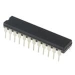
| 描述 | IC ADC 24BIT RTD I SOURCE 24-DIP模数转换器 - ADC CMOS 24B w/ Matched RTD Excitation Crnt |
| 产品分类 | |
| 品牌 | Analog Devices |
| 产品手册 | |
| 产品图片 |
|
| rohs | 符合RoHS无铅 / 符合限制有害物质指令(RoHS)规范要求 |
| 产品系列 | 数据转换器IC,模数转换器 - ADC,Analog Devices AD7711ANZ- |
| 数据手册 | |
| 产品型号 | AD7711ANZ |
| 产品目录页面 | |
| 产品种类 | 模数转换器 - ADC |
| 位数 | 24 |
| 供应商器件封装 | 24-PDIP |
| 信噪比 | 131 dB |
| 分辨率 | 24 bit |
| 包装 | 管件 |
| 商标 | Analog Devices |
| 安装类型 | 通孔 |
| 安装风格 | Through Hole |
| 封装 | Tube |
| 封装/外壳 | 24-DIP(0.300",7.62mm) |
| 封装/箱体 | PDIP-24 |
| 工作温度 | -40°C ~ 80°C |
| 工作电源电压 | 5 V |
| 工厂包装数量 | 15 |
| 接口类型 | Serial (3-Wire, 4-Wire) |
| 数据接口 | 串行 |
| 最大功率耗散 | 53 mW |
| 最大工作温度 | + 125 C |
| 最小工作温度 | - 55 C |
| 标准包装 | 15 |
| 特性 | PGA |
| 电压参考 | Internal, External |
| 电压源 | 模拟和数字,双 ± |
| 系列 | AD7711 |
| 结构 | Sigma-Delta |
| 转换器数 | 1 |
| 转换器数量 | 1 |
| 转换速率 | 1.028 kS/s |
| 输入数和类型 | 1 个单端,单极1 个单端,双极1 个差分,单极1 个差分,双极 |
| 输入类型 | Single-Ended |
| 通道数量 | 2 Channel |
| 采样率(每秒) | 1.03k |


PDF Datasheet 数据手册内容提取
LC2MOS Signal Conditioning ADC with RTD Excitation Currents AD7711 FEATURES FUNCTIONAL BLOCK DIAGRAM Charge-Balancing ADC REF REF 24 Bits, No Missing Codes AVDD DVDD IN (–) IN (+) VBIAS REF OUT (cid:4)0.0015% Nonlinearity AVDD 2-Channel Programmable Gain Front End 2.5V REFERENCE Gains from 1 to 128 4.5(cid:3)A 1 Differential Input CHARGE-BALANCING A/D CONVERTER 1 Single-Ended Input AIN1(+) LAobwili-tPya tsos RFielatedr/ Wwirtihte P Croaglibrarmatmioanb Cleo eFfiflticeire Cntustoffs AIN1(–) MU PGA AMUOTDOU(cid:1)-ZL-E(cid:2)ARTOOERD DFIIGLTITEARL SYNC RTD Excitation Current Sources X AIN2 A = 1–128 Bidirectional Microcontroller Serial Interface MCLK Internal/External Reference Option 200(cid:3)A AVDD GENCELROACTKION MINCLK Single- or Dual-Supply Operation RTD1 OUT Low Power (25 mW typ) with Power-Down Mode 200(cid:3)A SERIAL INTERFACE (7 mW typ) CONTROL OUTPUT RTD2 REGISTER REGISTER APPLICATIONS AD7711 RTD Transducers Process Control Smart Transmitters AGND DGND VSS RFS TFS MODE SDATA SCLKDRDY A0 Portable Industrial Instruments The AD7711 is ideal for use in smart, microcontroller based systems. Gain settings, signal polarity, input channel selection, GENERAL DESCRIPTION and RTD current control can be configured in software using The AD7711 is a complete analog front end for low frequency the bidirectional serial port. The AD7711 contains self- measurement applications. The device accepts low level signals calibration, system calibration, and background calibration directly from a transducer and outputs a serial digital word. It options, and also allows the user to read and write the on-chip employs a (cid:1)-(cid:2) conversion technique to realize up to 24 bits of calibration registers. no missing codes performance. The input signal is applied to a proprietary programmable gain front end based around an ana- CMOS construction ensures low power dissipation, and a software log modulator. The modulator output is processed by an on-chip programmable power-down mode reduces the standby power digital filter. The first notch of this digital filter can be pro- consumption to only 7 mW typical. The part is available in a grammed via the on-chip control register, allowing adjustment 24-lead, 0.3-inch-wide, plastic and hermetic dual-in-line pack- of the filter cutoff and settling time. age (DIP) as well as a 24-lead small outline (SOIC) package. The part features one differential analog input and one single- PRODUCT HIGHLIGHTS ended analog input as well as a differential reference input. 1. The programmable gain front end allows the AD7711 to Normally, one of the input channels will be used as the main accept input signals directly from an RTD transducer, channel with the second channel used as an auxiliary input to removing a considerable amount of signal conditioning. periodically measure a second voltage. It can be operated from a On-chip current sources provide excitation for 3-wire and single supply (by tying the V pin to AGND), provided that the SS 4-wire RTD configurations. input signals on the analog inputs are more positive than –30mV. By taking the V pin negative, the part can convert signals 2. No missing codes ensure true, usable, 23-bit dynamic range SS down to –VREF on its inputs. The part provides two current coupled with excellent ±0.0015% accuracy. The effects of sources that can be used to provide excitation in 3-wire and 4-wire temperature drift are eliminated by on-chip self-calibration, RTD configurations. The AD7711 thus performs all signal which removes zero-scale and full-scale errors. conditioning and conversion for a single- or dual-channel system. 3. The AD7711 is ideal for microcontroller or DSP processor applications with an on-chip control register that allows control over filter cutoff, input gain, channel selection, signal polarity, RTD current control, and calibration modes. 4. The AD7711 allows the user to read and to write the on-chip REV.G calibration registers. This means that the microcontroller has much greater control over the calibration procedure. Information furnished by Analog Devices is believed to be accurate and reliable. However, no responsibility is assumed by Analog Devices for its use, nor for any infringements of patents or other rights of third parties that may result from its use. No license is granted by implication or otherwise One Technology Way, P.O. Box 9106, Norwood, MA 02062-9106, U.S.A. under any patent or patent rights of Analog Devices. Trademarks and Tel: 781/329-4700 www.analog.com registered trademarks are the property of their respective owners. Fax: 781/326-8703 © 2004 Analog Devices, Inc. All rights reserved.
AD7711–SPECIFICATIONS (AV = +5V (cid:4) 5%; DV = +5V (cid:4) 5%; V = 0V or –5V (cid:4) 5%; REF IN(+) = DD DD SS +2.5V; REFIN(–) = AGND; MCLK IN = 10MHz unless otherwise stated. All specifications T to T , unless otherwise noted.) MIN MAX Parameter A, S Versions1 Unit Conditions/Comments STATIC PERFORMANCE No Missing Codes 24 Bits min Guaranteed by Design. For Filter Notches £ 60 Hz 22 Bits min For Filter Notch = 100 Hz 18 Bits min For Filter Notch = 250 Hz 15 Bits min For Filter Notch = 500 Hz 12 Bits min For Filter Notch = 1 kHz Output Noise See Tables I and II Depends on Filter Cutoffs and Selected Gain Integral Nonlinearity @ 25∞C ±0.0015 % FSR max Filter Notches £ 60 Hz TMIN to TMAX ±0.003 % FSR max Typically ±0.0003% Positive Full-Scale Error2, 3 See Note 4 Excluding Reference Full-Scale Drift5 1 mV/∞C typ Excluding Reference. For Gains of 1, 2 0.3 mV/∞C typ Excluding Reference. For Gains of 4, 8, 16, 32, 64, 128 Unipolar Offset Error2 See Note 4 Unipolar Offset Drift5 0.5 mV/∞C typ For Gains of 1, 2 0.25 mV/∞C typ For Gains of 4, 8, 16, 32, 64, 128 Bipolar Zero Error2 See Note 4 Bipolar Zero Drift5 0.5 mV/∞C typ For Gains of 1, 2 0.25 mV/∞C typ For Gains of 4, 8, 16, 32, 64, 128 Gain Drift 2 ppm/∞C typ Bipolar Negative Full-Scale Error2 @ 25∞C ±0.003 % FSR max Excluding Reference TMIN to TMAX ±0.006 % FSR max Typically ±0.0006% Bipolar Negative Full-Scale Drift5 1 mV/∞C typ Excluding Reference. For Gains of 1, 2 0.3 mV/∞C typ Excluding Reference. For Gains of 4, 8, 16, 32, 64, 128 ANALOG INPUTS/REFERENCE INPUTS Normal Mode 50 Hz Rejection6 100 dB min For Filter Notches of 10 Hz, 25 Hz, 50 Hz, ±0.02 ¥ fNOTCH Normal Mode 60 Hz Rejection6 100 dB min For Filter Notches of 10 Hz, 30 Hz, 60 Hz, ±0.02 ¥ fNOTCH DC Input Leakage Current @ 25∞C6 10 pA max T to T 1 nA max MIN MAX Sampling Capacitance6 20 pF max AIN1/REF IN Common-Mode Rejection (CMR) 100 dB min At DC and AV = 5 V DD Common-Mode Rejection (CMR) 90 dB min At DC and AV = 10 V DD Common-Mode 50 Hz Rejection6 150 dB min For Filter Notches of 10 Hz, 25 Hz, 50 Hz, ±0.02 ¥ fNOTCH Common-Mode 60 Hz Rejection6 150 dB min For Filter Notches of 10 Hz, 30 Hz, 60 Hz, ±0.02 ¥ fNOTCH Common-Mode Voltage Range7 V to AV V min to V max SS DD Analog Inputs8 Input Voltage Range9 For Normal Operation. Depends on Gain Selected 0 to +V 10 max Unipolar Input Range (B/U Bit of Control Register = 1) REF ±VREF max Bipolar Input Range (B/U Bit of Control Register = 0) Input Sampling Rate, f See Table III S AIN2 Offset Error 2.5 mV max Removed by System Calibrations but not by Self-Calibration AIN2 Offset Drift 1.5 mV/∞C typ Reference Inputs REF IN(+) – REF IN(–) Voltage11 +2.5 to +5 V min to V max For Specified Performance. Part Is Functional with Lower V Voltages REF Input Sampling Rate, f f /256 S CLK IN REFERENCE OUTPUT Output Voltage 2.5 V nom Initial Tolerance @ 25∞C ±1 % max Drift 20 ppm/∞C typ Output Noise 30 mV typ Peak-to-Peak Noise. 0.1 Hz to 10 Hz Bandwidth Line Regulation (AV ) 1 mV/V max DD Load Regulation 1.5 mV/mA max Maximum Load Current 1 mA External Current 1 mA max NOTES 1Temperature range is as follows: A Version = –40∞C to +85∞C; S Version = –55∞C to +125∞C. See also Note 16. 2Applies after calibration at the temperature of interest. 3Positive full-scale error applies to both unipolar and bipolar input ranges. 4These errors will be of the order of the output noise of the part, as shown in Table I, after system calibration. These errors will be 20mV typical after self-calibration or background calibration. 5Recalibration at any temperature or use of the background calibration mode will remove these drift errors. 6These numbers are guaranteed by design and/or characterization. 7This common-mode voltage range is allowed, provided the input voltage on AIN(+) and AIN(–) does not exceed AV + 30 mV and V – 30 mV. DD SS 8The analog inputs present a very high impedance dynamic load that varies with clock frequency and input sample rate. The maximum recommended source resis- tance depends on the selected gain (see Tables IV and V). 9The analog input voltage range on the AIN1(+) input is given here with respect to the voltage on the AIN1(–) input. The input voltage range on the AIN2 input is with respect to AGND. The absolute voltage on the analog inputs should not go more positive than AV + 30 mV, or more negative than V – 30 mV. DD SS 10V = REF IN(+) – REF IN(–). REF 11The reference input voltage range may be restricted by the input voltage range requirement on the V input. BIAS –2– REV. G
AD7711 Parameter A, S Versions1 Unit Conditions/Comments V INPUT12 BIAS Input Voltage Range AVDD – 0.85 ¥ VREF See VBIAS Input Section or AV – 3.5 V max Whichever Is Smaller; +5 V/–5 V or +10 V/0 V DD Nominal AV /V DD SS or AV – 2.1 V max Whichever Is Smaller; +5 V/0 V Nominal AV /V DD DD SS VSS + 0.85 ¥ VREF See VBIAS Input Section or V + 3 V min Whichever Is Greater; +5 V/–5 V or +10 V/0 V SS Nominal AV /V DD SS or V + 2.1 V min Whichever Is Greater; +5 V/0 V Nominal AV /V SS DD SS V Rejection 65 to 85 dB typ Increasing with Gain BIAS LOGIC INPUTS Input Current ±10 mA max All Inputs except MCLK IN V , Input Low Voltage 0.8 V max INL V , Input High Voltage 2.0 V min INH MCLK IN Only V , Input Low Voltage 0.8 V max INL V , Input High Voltage 3.5 V min INH LOGIC OUTPUTS V , Output Low Voltage 0.4 V max I = 1.6 mA OL SINK VOH, Output High Voltage 4.0 V min ISOURCE = 100 mA Floating State Leakage Current ±10 mA max Floating State Output Capacitance13 9 pF typ TRANSDUCER BURNOUT Current 4.5 mA nom Initial Tolerance @ 25∞C ±10 % typ Drift 0.1 %/∞C typ RTD EXCITATION CURRENTS (RTD1, RTD2) Output Current 200 mA nom Initial Tolerance @ 25∞C ±20 % max Drift 20 ppm/∞C typ Initial Matching @ 25∞C ±1 % max Matching between RTD1 and RTD2 Currents Drift Matching 3 ppm/∞C typ Matching between RTD1 and RTD2 Current Drift Line Regulation (AV ) 200 nA/V max AV = 5 V DD DD Load Regulation 200 nA/V max Output Compliance AV – 2 V max DD SYSTEM CALIBRATION Positive Full-Scale Calibration Limit14 (1.05 ¥ VREF)/GAIN V max GAIN Is the Selected PGA Gain (between 1 and 128) Negative Full-Scale Calibration Limit14 –(1.05 ¥ VREF)/GAIN V max GAIN Is the Selected PGA Gain (between 1 and 128) Offset Calibration Limit15 –(1.05 ¥ VREF)/GAIN V max GAIN Is the Selected PGA Gain (between 1 and 128) Input Span15 0.8 ¥ VREF/GAIN V min GAIN Is the Selected PGA Gain (between 1 and 128) (2.1 ¥ VREF)/GAIN V max GAIN Is the Selected PGA Gain (between 1 and 128) NOTES 12The AD7711 is tested with the following V voltages. With AV = 5 V and V = 0 V, V = 2.5 V; with AV = 10 V and V = 0 V, V = 5 V, and BIAS DD SS BIAS DD SS BIAS with AV = 5 V and V = –5 V, V = 0 V. DD SS BIAS 13Guaranteed by design, not production tested. 14After calibration, if the analog input exceeds positive full scale, the converter outputs all 1s. If the analog input is less than negative full scale, the device outputs all 0s. 15These calibration and span limits apply, provided the absolute voltage on the analog inputs does not exceed AV + 30 mV or go more negative than V – 30 mV. DD SS The offset calibration limit applies to both the unipolar zero point and the bipolar zero point. REV. G –3–
AD7711–SPECIFICATIONS Parameter A, S Versions1 Unit Conditions/Comments POWER REQUIREMENTS Power Supply Voltages AVDD Voltage16 5 to 10 V nom ±5% for Specified Performance DVDD Voltage17 5 V nom ±5% for Specified Performance AV – V Voltage 10.5 V max For Specified Performance DD SS Power Supply Currents AV Current 4 mA max DD DV Current 4.5 mA max DD V Current 1.5 mA max V = –5 V SS SS Power Supply Rejection18 Rejection w.r.t. AGND; Assumes V Is Fixed BIAS Positive Supply (AV and DV ) See Note 19 dB typ DD DD Negative Supply (V ) 90 dB typ SS Power Dissipation Normal Mode 45 mW max AV = DV = +5 V, V = 0 V; Typically 25 mW DD DD SS 52.5 mW max AV = DV = +5V, V = –5 V; Typically 30 mW DD DD SS Standby (Power-Down) Dissipation 15 mW max AV = DV = +5V, V = 0 V or –5 V; Typically 7 mW DD DD SS NOTES 16The AD7711 is specified with a 10 MHz clock for AVDD voltages of 5 V ± 5%. It is specified with an 8 MHz clock for AVDD voltages greater than 5.25 V and less than 10.5V. Operating with AVDD voltages in the range 5.25 V to 10.5 V is only guaranteed over the 0∞C to 70∞C temperature range. 17The ±5% tolerance on the DVDD input is allowed provided DVDD does not exceed AVDD by more than 0.3 V. 18Measured at dc and applies in the selected pass band. PSRR at 50 Hz will exceed 120 dB with filter notches of 10 Hz, 25 Hz, or 50 Hz. PSRR at 60 Hz will exceed 120 dB with filter notches of 10 Hz, 30 Hz, or 60 Hz. 19PSRR depends on gain: Gain of 1 = 70 dB typ; Gain of 2: 75 dB typ; Gain of 4 = 80 dB typ; Gains of 8 to 128 = 85 dB typ. These numbers can be improved (to 95 dB typ) by deriving the V voltage (via Zener diode or reference) from the AV supply. BIAS DD Specifications subject to change without notice. ABSOLUTE MAXIMUM RATINGS* REF OUT to AGND . . . . . . . . . . . . . . . . . . . . –0.3 V to AV DD (TA = 25∞C, unless otherwise noted.) Digital Input Voltage to DGND . . . . .–0.3 V to AVDD + 0.3 V Digital Output Voltage to DGND . . . –0.3 V to DV + 0.3 V AV to DV . . . . . . . . . . . . . . . . . . . . . . . –0.3 V to +12 V DD DD DD Operating Temperature Range AV to V . . . . . . . . . . . . . . . . . . . . . . . . . . –0.3 V to +12 V DD SS AV to AGND . . . . . . . . . . . . . . . . . . . . . . –0.3 V to +12 V Commercial (A Version) . . . . . . . . . . . . . . . .–40∞C to +85∞C DD AV to DGND . . . . . . . . . . . . . . . . . . . . . . –0.3 V to +12 V Extended (S Version) . . . . . . . . . . . . . . . . .–55∞C to +125∞C DD DV to AGND . . . . . . . . . . . . . . . . . . . . . . . –0.3 V to +6 V Storage Temperature Range . . . . . . . . . . . . .–65∞C to +150∞C DD DV to DGND . . . . . . . . . . . . . . . . . . . . . . . –0.3 V to +6 V Lead Temperature (Soldering, 10 secs) . . . . . . . . . . . . . 300∞C DD V to AGND . . . . . . . . . . . . . . . . . . . . . . . . . +0.3 V to –6 V Power Dissipation (Any Package) to 75∞C . . . . . . . . . .450 mW SS V to DGND . . . . . . . . . . . . . . . . . . . . . . . . . +0.3 V to –6 V *Stresses above those listed under Absolute Maximum Ratings may cause perma- SS Analog Input Voltage to AGND nent damage to the device. This is a stress rating only; functional operation of the . . . . . . . . . . . . . . . . . . . . . . . . . V – 0.3 V to AV + 0.3 V device at these or any other conditions above those listed in the operational SS DD sections of the specification is not implied. Exposure to absolute maximum rating Reference Input Voltage to AGND conditions for extended periods may affect device reliability. . . . . . . . . . . . . . . . . . . . . . . . . . V – 0.3 V to AV + 0.3 V SS DD ORDERING GUIDE Model Temperature Range Package Option* AD7711AN –40∞C to +85∞C N-24 AD7711AR –40∞C to +85∞C R-24 AD7711AR-REEL –40∞C to +85∞C R-24 AD7711AR-REEL7 –40∞C to +85∞C R-24 AD7711AQ –40∞C to +85∞C Q-24 AD7711SQ –55∞C to +125∞C Q-24 EVAL-AD7711EB Evaluation Board *N = Plastic DIP, Q = CERDIP, R = SOIC. CAUTION ESD (electrostatic discharge) sensitive device. Electrostatic charges as high as 4000 V readily accumulate on the human body and test equipment and can discharge without detection. Although the AD7711 features proprietary ESD protection circuitry, permanent damage may occur on devices subjected to high energy electrostatic discharges. Therefore, proper ESD precautions are recommended to avoid performance degradation or loss of functionality. –4– REV. G
AD7711 TIMING CHARACTERISTICS1, 2 (DVDD = +5V (cid:1) 5%; AVDD = +5V or +10 V3 (cid:1) 5%; VSS = 0 V or –5 V (cid:1) 10%; AGND = DGND = 0 V; f = 10MHz; Input Logic 0 = 0 V, Logic 1 = DV , unless otherwise noted.) CLK IN DD Limit at T , T MIN MAX Parameter (A, S Versions) Unit Conditions/Comments f 4, 5 400 kHz min Master Clock Frequency: Crystal Oscillator or Externally CLKIN Supplied for Specified Performance 10 MHz max 2 t 0.4 × t ns min Master Clock Input Low Time; t = 1/f CLK IN LO CLK IN CLK IN CLK IN t 0.4 × t ns min Master Clock Input High Time CLK IN HI CLK IN t6 50 ns max Digital Output Rise Time. Typically 20 ns r t6 50 ns max Digital Output Fall Time. Typically 20 ns f t 1000 ns min SYNC Pulse Width 1 Self-Clocking Mode t 0 ns min DRDY to RFS Setup Time 2 t 0 ns min DRDY to RFS Hold Time 3 t 2 × t ns min A0 to RFS Setup Time 4 CLK IN t 0 ns min A0 to RFS Hold Time 5 t 4 × t + 20 ns max RFS Low to SCLK Falling Edge 6 CLK IN t 7 4 × t + 20 ns max Data Access Time (RFS Low to Data Valid) 7 CLK IN t 7 t /2 ns min SCLK Falling Edge to Data Valid Delay 8 CLK IN t /2+ 30 ns max CLK IN t t /2 ns nom SCLK High Pulse Width 9 CLK IN t 3 × t /2 ns nom SCLK Low Pulse Width 10 CLK IN t 50 ns min A0 to TFS Setup Time 14 t 0 ns min A0 to TFS Hold Time 15 t 4 × t + 20 ns max TFS to SCLK Falling Edge Delay Time 16 CLK IN t 4 × t ns min TFS to SCLK Falling Edge Hold Time 17 CLK IN t 0 ns min Data Valid to SCLK Setup Time 18 t 10 ns min Data Valid to SCLK Hold Time 19 NOTES 1Guaranteed by design, not production tested. All input signals are specified with tr = tf = 5 ns (10% to 90% of 5 V) and timed from a voltage level of 1.6 V. 2See Figures 10 to 13. 3The AD7711 is specified with a 10 MHz clock for AV voltages of 5 V ± 5%. It is specified with an 8 MHz clock for AV voltages greater than 5.25V and less DD DD than 10.5V. 4CLK IN duty cycle range is 45% to 55%. CLK IN must be supplied whenever the AD7711 is not in STANDBY mode. If no clock is present in this case, the device can draw higher current than specified and possibly become uncalibrated. 5The AD7711 is production tested with f at 10 MHz (8 MHz for AV > 5.25 V). It is guaranteed by characterization to operate at 400kHz. CLK IN DD 6Specified using 10% and 90% points on waveform of interest. 7These numbers are measured with the load circuit of Figure 1 and defined as the time required for the output to cross 0.8 V or 2.4 V. REV.G –5–
AD7711 TIMING CHARACTERISTICS Limit at T , T MIN MAX Parameter (A, S Versions) Unit Conditions/Comments External Clocking Mode f f /5 MHz max Serial Clock Input Frequency SCLK CLK IN t 0 ns min DRDY to RFS Setup Time 20 t 0 ns min DRDY to RFS Hold Time 21 t22 2 ¥ tCLK IN ns min A0 to RFS Setup Time t 0 ns min A0 to RFS Hold Time 23 t247 4 ¥ tCLK IN ns max Data Access Time (RFS Low to Data Valid) t 7 10 ns min SCLK Falling Edge to Data Valid Delay 25 2 ¥ tCLK IN + 20 ns max t26 2 ¥ tCLK IN ns min SCLK High Pulse Width t27 2 ¥ tCLK IN ns min SCLK Low Pulse Width t t + 10 ns max SCLK Falling Edge to DRDY High 28 CLK IN t 8 10 ns min SCLK to Data Valid Hold Time 29 t + 10 ns max CLK IN t 10 ns min RFS/TFS to SCLK Falling Edge Hold Time 30 t318 5 ¥ tCLK IN/2 + 50 ns max RFS to Data Valid Hold Time t 0 ns min A0 to TFS Setup Time 32 t 0 ns min A0 to TFS Hold Time 33 t34 4 ¥ tCLK IN ns min SCLK Falling Edge to TFS Hold Time t35 2 ¥ tCLK IN – SCLK High ns min Data Valid to SCLK Setup Time t 30 ns min Data Valid to SCLK Hold Time 36 NOTES 8These numbers are derived from the measured time taken by the data output to change 0.5 V when loaded with the circuit of Figure 1. The measured number is then extrapolated back to remove effects of charging or discharging the 100 pF capacitor. This means that the times quoted in the Timing Characteristics are the true bus relinquish times of the part and, as such, are independent of external bus loading capacitances. Specifications subject to change without notice. PIN CONFIGURATION DIP AND SOIC 1.6mA SCLK 1 24 DGND MCLK IN 2 23 DVDD TO OUTPUT +2.1V MCLK OUT 3 22 SDATA PIN 100pF A0 4 21 DRDY SYNC 5 20 RFS AD7711 200(cid:3)A MODE 6 TOP VIEW 19 TFS AIN1(+) 7 (Not to Scale) 18 AGND Figure 1.Load Circuit for Access Time and Bus AIN1(–) 8 17 AIN2 Relinquish Time RTD1 9 16 REF OUT RTD2 10 15 REF IN(+) VSS 11 14 REF IN(–) AVDD 12 13 VBIAS –6– REV. G
AD7711 PIN FUNCTION DESCRIPTIONS Pin Mnemonic Function 1 SCLK Serial Clock. Logic input/output, depending on the status of the MODE pin. When MODE is high, the device is in its self-clocking mode, and the SCLK pin provides a serial clock output. This SCLK becomes active when RFS or TFS goes low, and goes high impedance when either RFS or TFS returns high or when the device has completed transmission of an output word. When MODE is low, the device is in its external clocking mode and the SCLK pin acts as an input. This input serial clock can be a continuous clock with all 2 data transmitted in a continuous train of pulses. Alternatively, it can be a noncontinuous clock with the information being transmitted to the AD7711 in smaller batches of data. 2 MCLK IN Master Clock Signal for the Device. This can be provided in the form of a crystal or external clock. A crystal can be tied across the MCLK IN and MCLK OUT pins. Alternatively, the MCLK IN pin can be driven with a CMOS-compatible clock and MCLK OUT left unconnected. The clock input frequency is nominally 10 MHz. 3 MCLK OUT When the master clock for the device is a crystal, the crystal is connected between MCLK IN and MCLK OUT. 4 A0 Address Input. With this input low, reading and writing to the device is to the control register. With this input high, access is to either the data register or the calibration registers. 5 SYNC Logic Input. Allows for synchronization of the digital filters when using a number of AD7711s. It resets the nodes of the digital filter. 6 MODE Logic Input. When this pin is high, the device is in its self-clocking mode; with this pin low, the device is in its external clocking mode. 7 AIN1(+) Analog Input Channel 1. Positive input of the programmable gain differential analog input. The AIN1(+) input is connected to an output current source that can be used to check that an external transducer has burned out or gone open circuit. This output current source can be turned on/off via the control register. 8 AIN1(–) Analog Input Channel 1. Negative input of the programmable gain differential analog input. 9 RTD1 Constant Current Output. A nominal 200mA constant current is provided at this pin; this current can be used as the excitation current for RTDs. This current can be turned on or off via the control register. 10 RTD2 Constant Current Output. A nominal 200mA constant current is provided at this pin; this current can be used as the excitation current for RTDs. This current can be turned on or off via the control register, and can be used to eliminate lead resistance errors in 3-wire RTD configurations. 11 V Analog Negative Supply, 0 V to –5 V. Tied to AGND for single-supply operation. The input voltage on AIN1 SS or AIN2 should not go > 30 mV negative w.r.t. V for correct operation of the device. SS 12 AV Analog Positive Supply Voltage, 5 V to 10 V. DD 13 VBIAS Input Bias Voltage. This input voltage should be set such that VBIAS + 0.85 ¥ VREF < AVDD and VBIAS – 0.85 ¥ VREF > VSS where VREF is REF IN(+) – REF IN(–). Ideally, this should be tied halfway between AVDD and V . Thus with AV = 5 V and V = 0 V, it can be tied to REF OUT; with AV = +5 V and SS DD SS DD V = –5 V, it can be tied to AGND; with AV = 10 V, it can be tied to 5 V. SS DD 14 REF IN(–) Reference Input. The REF IN(–) can lie anywhere between AV and V provided REF IN(+) is greater DD SS than REF IN(–). 15 REF IN(+) Reference Input. The reference input is differential provided REF IN(+) is greater than REF IN(–). REF IN(+) can lie anywhere between AV and V . DD SS 16 REF OUT Reference Output. The internal 2.5 V reference is provided at this pin. This is a single-ended output that is referred to AGND. It is a buffered output capable of providing 1 mA to an external load. 17 AIN2 Analog Input Channel 2. Single-ended programmable gain analog input. 18 AGND Ground Reference Point for Analog Circuitry. 19 TFS Transmit Frame Synchronization. Active low logic input used to write serial data to the device with serial data expected after the falling edge of this pulse. In the self-clocking mode, the serial clock becomes active after TFS goes low. During a write operation to the AD7711, the SDATA line should not return to high impedance until after TFS returns high. REV.G –7–
AD7711 Pin Mnemonic Function 20 RFS Receive Frame Synchronization. Active low logic input used to access serial data from the device. In the self-clocking mode, the SCLK and SDATA lines both become active after RFS goes low. In the external clocking mode, the SDATA line becomes active after RFS goes low. 21 DRDY Logic Output. A falling edge indicates that a new output word is available for transmission. The DRDY pin will return high upon completion of transmission of a full output word. DRDY is also used to indicate when the AD7711 has completed its on-chip calibration sequence. 22 SDATA Serial Data. Input/output with serial data being written to either the control register or the calibration registers and serial data being accessed from the control register, calibration registers, or the data register. During an output data read operation, serial data becomes active after RFS goes low (provided DRDY is low). During a write operation, valid serial data is expected on the rising edges of SCLK when TFS is low. The output data coding is natural binary for unipolar inputs and offset binary for bipolar inputs. 23 DV Digital Supply Voltage, 5 V. DV should not exceed AV by more than 0.3 V in normal operation. DD DD DD 24 DGND Ground Reference Point for Digital Circuitry. TERMINOLOGY Positive Full-Scale Overrange Intergral Nonlinearity Positive full-scale overrange is the amount of overhead avail- This is the maximum deviation of any code from a straight line able to handle input voltages on the AIN1(+) input greater passingthroughtheendpointsofthetransferfunction. The end- than AIN1(–) + V /GAIN or on the AIN2 input greater REF points of the transfer function are zero-scale (not to be confused than + V /GAIN (for example, noise peaks or excess REF withbipolarzero),apoint0.5LSBbelowthefirstcode transi- voltages due to system gain errors in system calibration rou- tion (000...000 to 000...001) and full scale, a point 0.5LSB tines) without introducing errors due to overloading the analog abovethelastcodetransition(111...110to 111...111). The modulator or to overflowing the digital filter. error is expressed as a percentage of full scale. Negative Full-Scale Overrange Positive Full-Scale Error This is the amount of overhead available to handle voltages on Positive full-scale error is the deviation of the last code transi- AIN1(+) below AIN1(–) – V /GAIN or on AIN2 below REF tion (111...110 to 111...111) from the ideal input full-scale –V /GAIN without overloading the analog modulator or over- REF voltage. For AIN1(+), the ideal full-scale input voltage is flowing the digital filter. Note that the analog input will accept (AIN1(–) + V /GAIN – 3/2 LSBs); for AIN2, the ideal full- negative voltage peaks on AIN1(+) even in the unipolar mode REF scale input voltage is V /GAIN – 3/2 LSBs. It applies to both provided that AIN1(+) is greater than AIN1(–) and greater than REF unipolar and bipolar analog input ranges. V – 30mV. SS Unipolar Offset Error Offset Calibration Range Unipolar offset error is the deviation of the first code transition In the system calibration modes, the AD7711 calibrates its from the ideal voltage. For AIN1(+), the ideal input voltage is offset with respect to the analog input. The offset calibration (AIN1(–) + 0.5 LSB); for AIN2, the ideal input is 0.5 LSB range specification defines the range of voltages that the AD7711 when operating in the unipolar mode. can accept and still calibrate offset accurately. Bipolar Zero Error Full-Scale Calibration Range This is the deviation of the midscale transition (0111...111 This is the range of voltages that the AD7711 can accept in the to 1000...000) fromtheideal input voltage. For AIN1(+), the system calibration mode and still calibrate full-scale correctly. ideal input voltage is (AIN1(–) – 0.5LSB); for AIN2, the ideal input is – 0.5 LSB when operating in the bipolar mode. Input Span In system calibration schemes, two voltages applied in sequence Bipolar Negative Full-Scale Error to the AD7711’s analog input define the analog input range. This is the deviation of the first code transition from the ideal The input span specification defines the minimum and maxi- input voltage. For (AIN1(+), the ideal input voltage is (AIN1(–) mum input voltages from zero- to full-scale that the AD7711 – V /GAIN + 0.5 LSB); for AIN2 the ideal input is – V /GAIN can accept and still calibrate gain accurately. REF REF + 0.5 LSB when operating in the bipolar mode. –8– REV. G
AD7711 CONTROL REGISTER (24 BITS) A write to the device with the A0 input low writes data to the control register. A read to the device with the A0 input low accesses the contents of the control register. The control register is 24 bits wide; 24 bits of data must be written to the registers or the data will not be loaded. In other words, it is not possible to write just the first 12-bits of data into the control register. If more than 24 clock pulses are provided before TFS returns high, then all clock pulses after the 24th clock pulse are ignored. Similarly, a read operation from the control register should access 24 bits of data. MSB 2 MD2 MD1 MD0 G2 G1 G0 CH PD WL RO BO B/U FS11 FS10 FS9 FS8 FS7 FS6 FS5 FS4 FS3 FS2 FS1 FS0 LSB Operating Mode MD2 MD1 MD0 Operating Mode 0 0 0 Normal Mode. This is the normal mode of operation where a read to the device with A0 high accesses data from the data register. This is the default condition of these bits after the internal power-on reset. 0 0 1 Activate Self-Calibration. This activates self-calibration on the channel selected by CH. This is a one-step calibration sequence, and when complete, the part returns to normal mode (with MD2, MD1, MD0 of the control register returning to 0, 0, 0). The DRDY output indicates when this self-calibration is complete. For this calibration type, the zero-scale calibration is done internally on shorted (zeroed) inputs, and the full-scale calibration is done internally on V . REF 0 1 0 Activate System Calibration. This activates system calibration on the channel selected by CH. This is a two-step calibration sequence, with the zero-scale calibration done first on the selected input channel and DRDY indicating when this zero-scale calibration is complete. The part returns to normal mode at the end of this first step in the two-step sequence. 0 1 1 Activate System Calibration. This is the second step of the system calibration sequence with full-scale calibration being performed on the selected input channel. Once again, DRDY indicates when the full- scale calibration is complete. When this calibration is complete, the part returns to normal mode. 1 0 0 Activate System Offset Calibration. This activates system offset calibration on the channel selected by CH. This is a one-step calibration sequence and, when complete, the part returns to normal mode with DRDY indicating when this system offset calibration is complete. For this calibration type, the zero-scale calibration is done on the selected input channel, and the full-scale calibration is done internally on V . REF 1 0 1 Activate Background Calibration. This activates background calibration on the channel selected by CH. If the background calibration mode is on, the AD7711 provides continuous self-calibration of the reference and shorted (zeroed) inputs. This calibration takes place as part of the conversion sequence, extending the conversion time and reducing the word rate by a factor of 6. The major advantage is that the user does not have to recalibrate the device when there is a change in the ambient temperature. In this mode, the shorted (zeroed) inputs and V , as well as the analog input voltage, are continuously moni- REF tored and the calibration registers of the device are automatically updated. 1 1 0 Read/Write Zero-Scale Calibration Coefficients. A read to the device with A0 high accesses the contents of the zero-scale calibration coefficients of the channel selected by CH. A write to the device with A0 high writes data to the zero-scale calibration coefficients of the channel selected by CH. The word length for reading and writing these coefficients is 24 bits, regardless of the status of the WL bit of the control register. Therefore, 24 bits of data must be written to the calibration register or the new data will not be transferred to the calibration register. 1 1 1 Read/Write Full-Scale Calibration Coefficients. A read to the device with A0 high accesses the contents of the full-scale calibration coefficients of the channel selected by CH. A write to the device with A0 high writes data to the full-scale calibration coefficients of the channel selected by CH. The word length for reading and writing these coefficients is 24 bits, regardless of the status of the WL bit of the control register. Therefore, 24 bits of data must be written to the calibration register, or the new data will not be transferred to the calibration register. REV.G –9–
AD7711 PGA Gain G2 Gl G0 Gain 0 0 0 1 (Default Condition after the Internal Power-On Reset) 0 0 1 2 0 1 0 4 0 1 1 8 1 0 0 16 1 0 1 32 1 1 0 64 1 1 1 128 CHANNEL SELECTION CH Channel 0 AIN1 (Default Condition after Internal Power-On Reset) 1 AIN2 Power-Down PD 0 Normal Operation (Default Condition after Internal Power-On Reset) 1 Power-Down Word Length WL Output Word Length 0 16-bit (Default Condition after Internal Power-On Reset) 1 24-bit RTD Excitation Current IO 0 Off (Default Condition after Internal Power-On Reset) 1 On Burnout Current BO 0 Off (Default Condition after Internal Power-On Reset) 1 On Bipolar/Unipolar Selection (Both Inputs) B/U 0 Bipolar (Default Condition after Internal Power-On Reset) 1 Unipolar FILTER SELECTION (FS11–FS0) time) for the device is equal to the frequency selected for the The on-chip digital filter provides a sinc3(or (sinx/x)3) filter first notch of the filter. For example, if the first notch of the response. The 12 bits of data programmed into these bits deter- filter is selected at 50 Hz, a new word is available at a 50 Hz rate mine the filter cutoff frequency, the position of the first notch of or every 20 ms. If the first notch is at 1 kHz, a new word is avail- the filter and the data rate for the part. In association with the able every 1 ms. gain selection, it also determines the output noise (and therefore The settling time of the filter to a full-scale step input change the effective resolution) of the device. is worst case 4 ¥ 1/(output data rate). This settling time is to The first notch of the filter occurs at a frequency determined by 100% of the final value. For example, with the first filter notch the relationship: filter first notch frequency = (f /512)/code at 50 Hz, the settling time of the filter to a full-scale step input CLK IN where code is the decimal equivalent of the code in bits FS0 to change is 80 ms max. If the first notch is at 1 kHz, the settling FS11 and is in the range 19 to 2,000. With the nominal f time of the filter to a full-scale input step is 4 ms max. This CLK IN of 10 MHz, this results in a first notch frequency range from settling time can be reduced to 3 ¥ 1/(output data rate) by syn- 9.76 Hz to 1.028 kHz. To ensure correct operation of the chronizing the step input change to a reset of the digital filter. In AD7711, the value of the code loaded to these bits must be other words, if the step input takes place with SYNC low, the within this range. Failure to do this will result in unspecified settling time is 3 ¥ 1/(output data rate). If a change of channels operation of the device. takes place, the settling time is 3 ¥ 1/(output data rate) regard- less of the SYNC input. Changing the filter notch frequency, as well as the selected gain, impacts resolution. Tables I and II and Figure 2 show the effect The –3 dB frequency is determined by the programmed first of the filter notch frequency and gain on the effective resolution notch frequency according to the relationship: of the AD7711. The output data rate (or effective conversion filter –3 dB frequency = 0.262 ¥ first notch frequency. –10– REV. G
AD7711 Tables I and II show the output rms noise for some typical notch frequencies. Meanwhile, device noise is added in the PGA notch and –3 dB frequencies. The numbers given are for the and, therefore, effective resolution suffers a little at high gains bipolar input ranges with a V of 2.5 V. These numbers are for lower notch frequencies. REF typical and are generated with an analog input voltage of 0 V. At the lower filter notch settings (below 60 Hz), the no missing The output noise from the part comes from two sources. The codes performance of the device is at the 24-bit level. At the higher first is the electrical noise in the semiconductor devices used in settings, more codes will be missed until at the 1 kHz notch setting, the implementation of the modulator (device noise). The second no missing codes performance is guaranteed only to the 12-bit occurs when the analog input signal is converted into the digital level. However, since the effective resolution of the part is 10.5 bits 2 domain adding quantization noise. The device noise is at a low for this filter notch setting, this no missing codes performance level and is largely independent of frequency. The quantization should be more than adequate for all applications. noise starts at an even lower level but rises rapidly with increas- ing frequency to become the dominant noise source. Conse- The effective resolution of the device is defined as the ratio of the quently, lower filter notch settings (below 60 Hz approximately) output rms noise to the input full scale. This does not remain tend to be device-noise dominated while higher notch settings constant with increasing gain or with increasing bandwidth. are dominated by quantization noise. Changing the filter notch Table II is the same as Table I except that the output is expressed and cutoff frequency in the quantization-noise dominated region in terms of effective resolution (the magnitude of the rms noise results in a more dramatic improvement in noise performance with respect to 2 ¥ VREF/GAIN, or the input full scale). It is pos- than it does in the device-noise dominated region as shown in sible to do post filtering on the device to improve the output data Table I. Furthermore, quantization noise is added after the PGA, rate for a given –3 dB frequency and also to further reduce the so effective resolution is independent of gain for the higher filter output noise (see the Digital Filtering section). Table I. Output Noise vs. Gain and First Notch Frequency First Notch of Typical Output RMS Noise ((cid:3)V) Filter and O/P –3dB Data Rate1 Frequency Gain of 1 Gain of 2 Gain of 4 Gain of 8 Gain of 16 Gain of 32 Gain of 64 Gain of 128 10Hz2 2.62Hz 1.0 0.78 0.48 0.33 0.25 0.25 0.25 0.25 25Hz2 6.55Hz 1.8 1.1 0.63 0.50 0.44 0.41 0.38 0.38 30Hz2 7.86Hz 2.5 1.31 0.84 0.57 0.46 0.43 0.4 0.4 50Hz2 13.1 Hz 4.33 2.06 1.2 0.64 0.54 0.46 0.46 0.46 60Hz2 15.72 Hz 5.28 2.36 1.33 0.87 0.63 0.62 0.6 0.56 100Hz3 26.2 Hz 13 6.4 3.7 1.8 1.1 0.9 0.65 0.65 250Hz3 65.5 Hz 130 75 25 12 7.5 4 2.7 1.7 500Hz3 131 Hz 0.6 ¥ 103 0.26 ¥ 103 140 70 35 25 15 8 1kHz3 262 Hz 3.1 ¥ 103 1.6 ¥ 103 0.7 ¥ 103 0.29 ¥ 103 180 120 70 40 NOTES 1The default condition (after the internal power-on reset) for the first notch of filter is 60 Hz. 2For these filter notch frequencies, the output rms noise is primarily dominated by device noise, and, as a result, is independent of the value of the reference voltage. Therefore, increasing the reference voltage will give an increase in the effective resolution of the device (that is, the ratio of the rms noise to the input full scale is increased because the output rms noise remains constant as the input full scale increases). 3For these filter notch frequencies, the output rms noise is dominated by quantization noise, and, as a result, is proportional to the value of the reference voltage. Table II. Effective Resolution vs. Gain and First Notch Frequency First Notch of Effective Resolution* (Bits) Filter and O/P –3dB Data Rate Frequency Gain of 1 Gain of 2 Gain of 4 Gain of 8 Gain of 16 Gain of 32 Gain of 64 Gain of 128 10Hz 2.62Hz 22.5 21.5 21.5 21 20.5 19.5 18.5 17.5 25Hz 6.55Hz 21.5 21 21 20 19.5 18.5 17.5 16.5 30Hz 7.86Hz 21 21 20.5 20 19.5 18.5 17.5 16.5 50Hz 13.1Hz 20 20 20 20 19 18.5 17.5 16.5 60Hz 15.72Hz 20 20 20 19.5 19 18 17 16 100Hz 26.2Hz 18.5 18.5 18.5 18.5 18 17.5 17 16 250Hz 65.5Hz 15 15 15.5 15.5 15.5 15.5 15 14.5 500Hz 131Hz 13 13 13 13 13 12.5 12.5 12.5 1kHz 262Hz 10.5 10.5 11 11 11 10.5 10 10 *Effective resolution is defined as the magnitude of the output rms noise with respect to the input full scale (i.e., 2 ¥ VREF/GAIN). The above table applies for a V of 2.5 V and resolution numbers are rounded to the nearest 0.5 LSB. REF REV.G –11–
AD7711 Figure 2 shows similar information to that outlined in Table I. A/D converter (sigma-delta modulator) converts the sampled In these plots, however, the output rms noise is shown for the signal into a digital pulse train whose duty cycle contains the full range of available cutoffs frequencies. The numbers given in digital information. The programmable gain function on the these plots are typical values at 25∞C. analog input is also incorporated in this sigma-delta modulator with the input sampling frequency being modified to give the higher gains. A sinc3 digital low-pass filter processes the out- 10000 put of the sigma-delta modulator and updates the output GAIN OF 1 register at a rate determined by the first notch frequency of GAIN OF 2 this filter. The output data can be read from the serial port 1000 GAIN OF 4 randomly or periodically at any rate up to the output register GAIN OF 8 V update rate. The first notch of this digital filter (and therefore (cid:3) E – 100 its –3 dB frequency) can be programmed via an on-chip con- S OI trol register. The programmable range for this first notch N T frequency is 9.76 Hz to 1.028 kHz, giving a programmable range U P 10 for the –3 dB frequency of 2.58 Hz to 269 Hz. T U O The basic connection diagram for the part is shown in Figure 3. 1 This figure shows the AD7711 in the external clocking mode with both the AV and DV pins of the AD7711 being driven DD DD from the analog 5 V supply. Some applications have separate 0.1 10 100 1000 10000 supplies for both AVDD and DVDD, and in some cases, the ana- NOTCH FREQUENCY – Hz log supply exceeds the 5 V digital supply (see the Power Sup- Figure 2a.Output Noise vs. Gain and Notch plies and Grounding section). Frequency (Gains of 1 to 8) ANALOG +5V SUPPLY 10(cid:3)F 0.1(cid:3)F 0.1(cid:3)F 1000 AVDD DVDD GAIN OF 16 DIFFERENTIAL AIN1(+) DRDY DATA READY 100 GAIN OF 32 ANALOG INPUT AIN1(–) TFS TRANSMIT (WRITE) (cid:3)– V GAIN OF 64 ASINNAGLLOEG-E INNDPEUDT AIN2 AD7711 RFS RECEIVE (READ) SE GAIN OF 128 RTD1 SDATA SERIAL DATA T NOI 10 RTD2 SCLK SERIAL CLOCK U ANALOG GROUND AGND P A0 ADDRESS INPUT UT VSS O DIGITAL GROUND DGND MODE 1 REF OUT SYNC +5V REF IN(+) MCLK OUT VBIAS 0.1 REF IN(–) MCLK IN 10 100 1000 10000 NOTCH FREQUENCY – Hz Figure 2b.Output Noise vs. Gain and Notch Figure 3.Basic Connection Diagram Frequency (Gains of 16 to 128) The AD7711 provides a number of calibration options that can be programmed via the on-chip control register. A calibration CIRCUIT DESCRIPTION cycle may be initiated at any time by writing to this control The AD7711 is a sigma-delta A/D converter with on-chip digital register. The part can perform self-calibration using the on-chip filtering for measuring wide dynamic range, low frequency signals calibration microcontroller and SRAM to store calibration such as those in RTD applications, industrial control, or process parameters. Other system components may also be included in control applications. It contains a sigma-delta (or charge-bal- the calibration loop to remove offset and gain errors in the input ancing) ADC, a calibration microcontroller with on-chip static channel using the system calibration mode. Another option is a RAM, a clock oscillator, a digital filter, and a bidirectional serial background calibration mode where the part continuously communications port. performs self-calibration and updates the calibration coeffi- The part contains two analog input channels, a programmable cients. Once the part is in this mode, the user does not have to gain differential analog input, and a programmable gain single- issue periodic calibration commands to the device or recalibrate ended input. The gain range is from 1 to 128 allowing the part when there is a change in the ambient temperature or power to accept unipolar signals of 0 mV to 20 mV and 0 V to 2.5 V supply voltage. or bipolar signals in the range ±20 mV to ±2.5 V when the The AD7711 gives the user access to the on-chip calibration reference input voltage equals 2.5 V. The input signal to the registers, allowing the microprocessor to read the device calibra- selected analog input channel is continuously sampled at a tion coefficients and also to write its own calibration coefficients rate determined by the frequency of the master clock, MCLK to the part from prestored values in E2PROM. This gives the IN, and the selected gain (see Table III). A charge-balancing –12– REV. G
AD7711 microprocessor much greater control over the AD7711’s cali- low-pass filter or integrator. It also illustrates the derivation of bration procedure. It also means that the user can verify the the alternative name for these devices, charge-balancing ADCs. calibration is correct by comparing the coefficients after calibra- tion with prestored values in E2PROM. DIFFERENTIAL AMPLIFIER INTEGRATOR The AD7711 can be operated in single-supply systems provided COMPARATOR that the analog input voltage does not go more negative than VIN (cid:1) –30 mV. For larger bipolar signals, a V of –5 V is required by SS the part. For battery operation, the AD7711 also offers a pro- 2 +FS grammable standby mode that reduces idle power consumption to typically 7 mW. DAC –FS THEORY OF OPERATION Figure 5.Basic Charge-Balancing ADC The general block diagram of a sigma-delta ADC is shown in The device consists of a differential amplifier (whose output is Figure 4. It contains the following elements: the difference between the analog input and the output of a ∑ A sample-hold amplifier. 1-bit DAC), an integrator, and a comparator. The term charge- ∑ A differential amplifier or subtracter. balancing comes from the fact that this system is a negative feedback loop that tries to keep the net charge on the integrator ∑ An analog low-pass filter. capacitor at zero, by balancing charge injected by the input ∑ A 1-bit A/D converter (comparator). voltage with charge injected by the 1-bit DAC. When the analog ∑ A 1-bit DAC. input is zero, the only contribution to the integrator output ∑ A digital low-pass filter. comes from the 1-bit DAC. For the net charge on the integrator capacitor to be zero, the DAC output must spend half its time at +FS and half its time at –FS. Assuming ideal components, the COMPARATOR S/H AMP duty cycle of the comparator will be 50%. + ANALOG LOW-PASS DIGITAL – FILTER FILTER When a positive analog input is applied, the output of the 1-bit DAC must spend a larger proportion of the time at +FS, so the DIGITAL duty cycle of the comparator increases. When a negative input DAC DATA voltage is applied, the duty cycle decreases. Figure 4.General Sigma-Delta ADC The AD7711 uses a second-order sigma-delta modulator and a In operation, the analog signal sample is fed to the subtracter, digital filter that provides a rolling average of the sampled out- along with the output of the 1-bit DAC. The filtered difference put. After power-up, or if there is a step change in the input signal is fed to the comparator, which samples the difference voltage, there is a settling time that must elapse before valid signal at a frequency many times that of the analog signal sampling data is obtained. frequency (oversampling). Input Sample Rate Oversampling is fundamental to the operation of sigma-delta The modulator sample frequency for the device remains at ADCs. Using the quantization noise formula for an ADC, fCLK IN/512 (19.5 kHz @ fCLK IN = 10 MHz) regardless of the SNR = (6.02 ¥ number of bits + 1.76) dB, sceolmecbteinda gtiaoinn .o Hf mowueltvieprl,e ginaipnust gsraematpelre tsh paenr ¥m1o adrue laactohri ecvyecdle b ayn ad a 1-bit ADC or comparator yields an SNR of 7.78 dB. scaling the ratio of reference capacitor to input capacitor. As a The AD7711 samples the input signal at a frequency of 39 kHz or result of the multiple sampling, the input sample rate of greater (see Table III). As a result, the quantization noise is the device varies with the selected gain (see Table III). The spread over a much wider frequency than that of the band of effective input impedance is 1/C ¥ fS where C is the input sam- interest. The noise in the band of interest is reduced still further pling capacitance and fS is the input sample rate. by analog filtering in the modulator loop, which shapes the quantization noise spectrum to move most of the noise energy to Table III. Input Sampling Frequency vs. Gain frequencies outside the bandwidth of interest. The noise perfor- Gain Input Sampling Frequency (f ) mance is thus improved from this 1-bit level to the performance S outlined in Tables I and II and in Figure 2. 1 f /256 (39 kHz @ f = 10 MHz) CLK IN CLK IN The output of the comparator provides the digital input for the 2 2 ¥ fCLK IN/256 (78 kHz @ fCLK IN = 10 MHz) 1-bit DAC, so that the system functions as a negative feedback 4 4 ¥ fCLK IN/256 (156 kHz @ fCLK IN = 10 MHz) loop that tries to minimize the difference signal. The digital data 8 8 ¥ fCLK IN/256 (312 kHz @ fCLK IN = 10 MHz) that represents the analog input voltage is contained in the duty 16 8 ¥ fCLK IN/256 (312 kHz @ fCLK IN = 10 MHz) cycle of the pulse train appearing at the output of the compara- 32 8 ¥ fCLK IN/256 (312 kHz @ fCLK IN = 10 MHz) tor. It can be retrieved as a parallel binary data-word using a 64 8 ¥ fCLK IN/256 (312 kHz @ fCLK IN = 10 MHz) digital filter. 128 8 ¥ fCLK IN/256 (312 kHz @ fCLK IN = 10 MHz) Sigma-delta ADCs are generally described by the order of the analog low-pass filter. A simple example of a first-order sigma- DIGITAL FILTERING delta ADC is shown in Figure 5. This contains only a first-order The AD7711’s digital filter behaves like a similar analog filter, with a few minor differences. REV.G –13–
AD7711 First, since digital filtering occurs after the A-to-D conversion notch frequency of the filter. Since the output data rate ex- process, it can remove noise injected during the conversion ceeds the Nyquist criterion, the output rate for a given band- process. Analog filtering cannot do this. width will satisfy most application requirements. However, there may be some applications that require a higher data rate On the other hand, analog filtering can remove noise super- for a given bandwidth and noise performance. Applications imposed on the analog signal before it reaches the ADC. Digital that need this higher data rate will require some post filtering filtering cannot do this, and noise peaks riding on signals near following the digital filter of the AD7711. full scale have the potential to saturate the analog modulator and digital filter, even though the average value of the signal is For example, if the required bandwidth is 7.86 Hz but the required within limits. To alleviate this problem, the AD7711 has update rate is 100 Hz, the data can be taken from the AD7711 overrange headroom built into the sigma-delta modulator and at the 100 Hz rate giving a –3 dB bandwidth of 26.2 Hz. Post digital filter, which allows overrange excursions of 5% above the filtering can be applied to this to reduce the bandwidth and analog input range. If noise signals are larger than this, consid- output noise to the 7.86 Hz bandwidth level, while maintaining eration should be given to analog input filtering, or to reducing an output rate of 100 Hz. the input channel voltage so that its full scale is half that of the Post filtering can also be used to reduce the output noise from analog input channel full scale. This will provide an overrange the device for bandwidths below 2.62 Hz. At a gain of 128, the capability greater than 100% at the expense of reducing the output rms noise is 250 nV. This is essentially device noise or dynamic range by 1 bit (50%). white noise, and since the input is chopped, the noise has a flat Filter Characteristics frequency response. By reducing the bandwidth below 2.62 Hz, The cutoff frequency of the digital filter is determined by the the noise in the resultant pass band can be reduced. A reduction value loaded to Bits FS0 to FS11 in the control register. At the in bandwidth by a factor of 2 results in a ÷2 reduction in the maximum clock frequency of 10 MHz, the minimum cutoff output rms noise. This additional filtering will result in a longer frequency of the filter is 2.58 Hz while the maximum program- settling time. mable cutoff frequency is 269 Hz. Antialias Considerations Figure 6 shows the filter frequency response for a cutoff fre- The digital filter does not provide any rejection at integer mul- quency of 2.62 Hz, which corresponds to a first filter notch fre- tiples of the modulator sample frequency (n ¥ 19.5 kHz, where quency of 10 Hz. This is a (sinx/x)3 response (also called sinc3) n = 1, 2, 3 . . . ). This means that there are frequency bands, that provides >100 dB of 50 Hz and 60 Hz rejection. Program- ±f3 dB wide (f3 dB is the cutoff frequency selected by FS0 to FS11), ming a different cutoff frequency via FS0–FS11 does not alter where noise passes unattenuated to the output. However, due to the profile of the filter response; it changes the frequency of the the AD7711’s high oversampling ratio, these bands occupy only notches as outlined in the Control Register section. a small fraction of the spectrum, and most broadband noise is filtered. In any case, because of the high oversampling ratio a 0 simple, RC, single-pole filter is generally sufficient to attenuate –20 the signals in these bands on the analog input and thus provide –40 adequate antialiasing filtering. –60 If passive components are placed in front of the AD7711, care –80 must be taken to ensure that the source impedance is low enough dB–100 so as not to introduce gain errors in the system. The dc input – AIN –120 impedance for the AD7711 is over 1 GW. The input appears as G–140 a dynamic load that varies with the clock frequency and with the –160 selected gain (see Figure 7). The input sample rate, as shown –180 in Table III, determines the time allowed for the analog input –200 capacitor, CIN, to be charged. External impedances result in a –220 longer charge time for this capacitor, which may result in gain errors being introduced on the analog inputs. Table IV shows the –240 0 10 20 30 40 50 60 allowable external resistance/capacitance values such that no FREQUENCY – Hz gain error to the 16-bit level is introduced while Table V shows Figure 6.Frequency Response of AD7711 Filter the allowable external resistance/capacitance values such that no Since the AD7711 contains this on-chip, low-pass filtering, gain error to the 20-bit level is introduced. Both inputs of the there is a settling time associated with step function inputs, and differential input channel (AIN1) look into similar input circuitry. data on the output will be invalid after a step change until the settling time has elapsed. The settling time depends upon the notch frequency chosen for the filter. The output data rate AD7711 equates to this filter notch frequency and the settling time of the 7kR(cid:5)I NTTYP HIGH filter to a full-scale step input is four times the output data AIN IMPEDANCE >1G(cid:5) period. In applications using both input channels, the settling CINT 11.5pF TYP time of the filter must be allowed to elapse before data from the second channel is accessed. VBIAS SWITCHING FREQUENCY DEPENDS Post Filtering ON fCLKIN AND SELECTED GAIN The on-chip modulator provides samples at a 19.5 kHz output rate. The on-chip digital filter decimates these samples to provide Figure 7.Analog Input Impedance data at an output rate that corresponds to the programmed first –14– REV. G
AD7711 Table IV. External Series Resistance That Will Not Introduce For 4-wire RTD applications, one of these excitation currents is 16-Bit Gain Error used to provide the excitation current for the RTD; the second current source can be left unconnected. For 3-wire RTD con- External Capacitance (pF) figurations, the second on-chip current source can be used to Gain 0 50 100 500 1000 5000 eliminate errors due to voltage drops across lead resistances. Figures 19 to 21 in the Applications section show some RTD 1 184 kW 45.3 kW 27.1 kW 7.3 kW 4.1 kW 1.1 kW configurations with the AD7711. 2 88.6 kW 22.1 kW 13.2 kW 3.6 kW 2.0 kW 560 W 4 41.4 kW 10.6 kW 6.3 kW 1.7 kW 970 W 270 W The temperature coefficient of the RTD current sources is 2 8–128 17.6 kW 4.8 kW 2.9 kW 790 W 440 W 120 W typically 20 ppm/∞C with a typical matching between the tem- perature coefficients of both current sources of 3 ppm/∞C. For applications where the absolute value of the temperature coeffi- Table V. External Series Resistance That Will Not Introduce cient is too large, the following schemes can be used to remove 20-Bit Gain Error the drift error. External Capacitance (pF) The conversion result from the AD7711 is ratiometric to the Gain 0 50 100 500 1000 5000 VREF voltage. Therefore, if the VREF voltage varies with the RTD temperature coefficient, the temperature drift from the current 1 145 kW 34.5 kW 20.4 kW 5.2 kW 2.8 kW 700 W source will be removed. For 4-wire RTD applications, the refer- 2 70.5 kW 16.9 kW 10 kW 2.5 kW 1.4 kW 350 W ence voltage can be made ratiometric to RTD current source 4 31.8 kW 8.0 kW 4.8 kW 1.2 kW 670 W 170 W by using the second current with a low TC resistor to generate 8–128 13.4 kW 3.6 kW 2.2 kW 550 W 300 W 80 W the reference voltage for the part. In this case, if a 12.5kW The numbers in Tables IV and V assume a full-scale change resistor is used, the 200mA current source generates 2.5V across the resistor. This 2.5V can be applied to the REF IN(+) input on the analog input. In any case, the error introduced due to of the AD7711 and with the REF IN(–) input at ground, it will longer charging times is a gain error that can be removed using supply a V of 2.5 V for the part. For 3-wire RTD configura- the system calibration capabilities of the AD7711, provided REF tions, the reference voltage for the part is generated by placing a the resultant span is within the limits of the system calibration techniques. low TC resistor (12.5kW for 2.5 V reference) in series with one of the constant current sources. The RTD current sources can be driven to within 2 V of AV . The reference input of the ANALOG INPUT FUNCTIONS DD AD7711 is differential so the REF IN(+) and REF IN(–) of the Analog Input Ranges AD7711 are driven from either side of the resistor. Both schemes Both analog inputs are programmable gain input channels that ensure that the reference voltage for the part tracks the RTD can handle either unipolar or bipolar input signals. The AIN1 current sources over temperature and, thereby, remove the channel is a differential channel with a common-mode range temperature drift error. from V to AV , provided the absolute value of the analog SS DD input voltage lies between V – 30 mV and AV + 30 mV. Bipolar/Unipolar Inputs SS DD The AIN2 input channel is a single-ended input that is referred The two analog inputs on the AD7711 can accept either unipo- to as AGND. lar or bipolar input voltage ranges. Bipolar or unipolar options are chosen by programming the B/U bit of the control register. The dc input leakage current is 10 pA maximum at 25∞C (±1 nA This programs both channels for either unipolar or bipolar over temperature). This results in a dc offset voltage developed operation. Programming the part for either type of operation across the source impedance. However, this dc offset effect can does not change any of the input signal conditioning; it simply be compensated for by a combination of the differential input changes the data output coding, using binary for unipolar inputs capability of the part and its system calibration mode. and offset binary for bipolar inputs. Burnout Current The AIN1 input channel is differential and, as a result, the The AIN1(+) input of the AD7711 contains a 4.5 mA current voltage to which the unipolar and bipolar signals are referenced source that can be turned on/off via the control register. This is the voltage on the AIN1(–) input. For example, if AIN1(–) is current source can be used in checking that a transducer has not 1.25 V and the AD7711 is configured for unipolar operation burned out or gone open circuit before attempting to take mea- with a gain of 1 and a V of 2.5 V, the input voltage range on surements on that channel. If the current is turned on and REF the AIN1(+) input is 1.25 V to 3.75 V. If AIN1(–) is 1.25 V, allowed to flow into the transducer and a measurement of the and the AD7711 is configured for bipolar mode with a gain of input voltage on the AIN1 input is taken, it can indicate that the 1 and a V of 2.5 V, the analog input range on the AIN1(+) transducer has burned out or gone open circuit. For normal REF input is –1.25 V to +3.75 V. For the AIN2 input, the input operation, this burnout current is turned off by writing a 0 to signals are referenced to AGND. the BO bit in the control register. RTD Excitation Current REFERENCE INPUT/OUTPUT The AD7711 also contains two matched 200 mA constant cur- The AD7711 contains a temperature compensated 2.5 V reference rent sources that are provided at the RTD1 and RTD2 pins of that has an initial tolerance of ±1%. This reference voltage is the device. These currents can be turned on/off via the control provided at the REF OUT pin, and it can be used as the reference register. Writing a 1 to the RO bit of the control register enables voltage for the part by connecting the REF OUT pin to the REF these excitation currents. REV.G –15–
AD7711 IN(+) pin. This REF OUT pin is a single-ended output, refer- For maximum internal headroom, the V voltage should be BIAS enced to AGND, which is capable of providing up to 1 mA to set halfway between AV and V . The difference between DD SS an external load. In applications where REF OUT is connected AVDD and (VBIAS + 0.85 ¥ VREF) determines the amount of directly to REF IN(+), REF IN(–) should be tied to AGND to headroom the circuit has at the upper end, while the difference provide the nominal 2.5 V reference for the AD7711. between VSS and (VBIAS – 0.85 ¥ VREF) determines the amount of headroom the circuit has at the lower end. When choosing a The reference inputs of the AD7711, REF IN(+) and REF IN(–), V voltage, ensure that it stays within prescribed limits. For provide a differential reference input capability. The common- BIAS single 5 V operation, the selected V voltage must ensure that mode range for these differential inputs is from V to AV . BIAS SS DD The nominal differential voltage, V (REF IN(+) – REF IN(–)), VBIAS ± 0.85 ¥ VREF does not exceed AVDD or VSS or that the REF V voltage itself is greater than V + 2.1 V and less than is 2.5 V for specified operation, but the reference voltage can go BIAS SS to 5 V with no degradation in performance if the absolute value AVDD – 2.1 V. For single 10 V operation or dual ±5 V opera- of REF IN(+) and REF IN(–) does not exceed its AV and tion, the selected VBIAS voltage must ensure that VBIAS ¥ 0.85 ¥ DD V does not exceed AV or V or that the V voltage V limits and the V input voltage range limits are obeyed. REF DD SS BIAS SS BIAS itself is greater than V + 3 V or less than AV – 3 V. For The part is also functional with V voltages down to 1 V but with SS DD REF example, with AV = 4.75 V, V = 0 V, and V = 2.5 V, the degraded performance because the output noise will, in terms DD SS REF allowable range for the V voltage is 2.125 V to 2.625 V. With of LSB size, be larger. REF IN(+) must always be greater than BIAS AV = 9.5 V, V = 0 V, and V = 5 V, the range for V REF IN(–) for correct operation of the AD7711. DD SS REF BIAS is 4.25 V to 5.25 V. With AV = +4.75 V, V = –4.75 V, DD SS Both reference inputs provide a high impedance, dynamic load and V = +2.5 V, the V range is –2.625 V to +2.625 V. REF BIAS similar to the analog inputs. The maximum dc input leakage The V voltage does have an effect on the AV power sup- current is 10 pA (±1 nA over temperature), and source resis- BIAS DD ply rejection performance of the AD7711. If the V voltage tance may result in gain errors on the part. The reference inputs BIAS tracks the AV supply, it improves the power supply rejection look like the analog input (see Figure 7). In this case, R is DD INT from the AV supply line from 80 dB to 95 dB. Using an 5 kW typ and CINT varies with gain. The input sample rate is DD external Zener diode connected between the AV line and f /256 and does not vary with gain. For gains of 1 to 8, C DD CLK IN INT V as the source for the V voltage gives the improvement is 20 pF; for a gain of 16, it is 10 pF; for a gain of 32, it is 5 pF; for BIAS BIAS in AV power supply rejection performance. a gain of 64, it is 2.5 pF; and for a gain of 128, it is 1.25 pF. DD The digital filter of the AD7711 removes noise from the refer- USING THE AD7711 ence input just as it does with the analog input, and the same SYSTEM DESIGN CONSIDERATIONS limitations apply regarding lack of noise rejection at integer The AD7711 operates differently from successive approxima- multiples of the sampling frequency. The output noise perfor- tion ADCs or integrating ADCs. Because it samples the signal mance outlined in Tables I and II assumes a clean reference. If continuously, like a tracking ADC, there is no need for a start the reference noise in the bandwidth of interest is excessive, it convert command. The output register is updated at a rate can degrade the performance of the AD7711. Using the on-chip determined by the first notch of the filter, and the output can reference as the reference source for the part (connecting be read at any time, either synchronously or asynchronously. REF OUT to REF IN) results in degraded output noise perfor- Clocking mance from the AD7711 for portions of the noise table that are The AD7711 requires a master clock input, which may be an dominated by the device noise. The on-chip reference noise external TTL/CMOS compatible clock signal applied to the effect is eliminated in ratiometric applications where the refer- MCLK IN pin with the MCLK OUT pin left unconnected. ence is used to provide the excitation voltage for the analog Alternatively, a crystal of the correct frequency can be connected front end. The connection shown in Figure 8 is recommended between MCLK IN and MCLK OUT, in which case the clock when using the on-chip reference. Recommended reference circuit will function as a crystal-controlled oscillator. For lower voltage sources for the AD7711 include the AD580 and AD680 clock frequencies, a ceramic resonator may be used instead of 2.5 V references. the crystal. For these lower frequency oscillators, external capacitors may be required on either the ceramic resonator or on the crystal. REF OUT REF IN(+) The input sampling frequency, the modulator sampling frequency, the –3 dB frequency, the output update rate, and the calibration REF IN(–) AD7711 time are all directly related to the master clock frequency, f Reducing the master clock frequency by a factor of 2 will CLK IN. Figure 8.REF OUT/REF IN Connection halve the above frequencies and update rate and will double the calibration time. V Input BIAS The V input determines at what voltage the internal analog The current drawn from the DV power supply is also directly BIAS DD circuitry is biased. It essentially provides the return path for related to f . Reducing f by a factor of 2 will halve the CLK IN CLK IN analog currents flowing in the modulator and, as such, it should DV current but will not affect the current drawn from the DD be driven from a low impedance point to minimize errors. AV power supply. DD System Synchronization If multiple AD7711s are operated from a common master clock, they can be synchronized to update their output registers simul- taneously. A falling edge on the SYNC input resets the filter and –16– REV. G
AD7711 places the AD7711 into a consistent, known state. A common going low. If DRDY is low before (or goes low during) the cali- signal to the AD7711s’ SYNC inputs will synchronize their bration command, it may take up to one modulator cycle before operation. This would typically be done after each AD7711 has DRDY goes high to indicate that calibration is in progress. performed its own calibration or has had calibration coefficients Therefore, DRDY should be ignored for up to one modulator loaded to it. cycle after the last bit of the calibration command is written to the control register. The SYNC input can also be used to reset the digital filter in systems where the turn-on time of the digital power supply Self-Calibration (DV ) is very long. In such cases, the AD7711 starts operat- In the self-calibration mode with a unipolar input range, the 2 DD ing internally before the DV line has reached its minimum zero-scale point used in determining the calibration coefficients DD operating level, 4.75 V. With a low DV voltage, the is with both inputs shorted (that is, AIN1(+) = AIN1(–) = DD AD7711’s internal digital filter logic does not operate correctly. V for AIN1 and AIN2 = V for AIN2), and the full-scale BIAS BIAS Thus, the AD7711 may have clocked itself into an incorrect point is V . The zero-scale coefficient is determined by con- REF operating condition by the time DV has reached its correct verting an internal shorted input node. The full-scale coefficient DD level. The digital filter is reset upon issue of a calibration com- is determined from the span between this shorted input conver- mand (whether it is self-calibration, system calibration, or back- sion and a conversion on an internal V node. The self- REF ground calibration) to the AD7711. This ensures correct calibration mode is invoked by writing the appropriate values operation of the AD7711. In systems where the power-on de- (0, 0, 1) to the MD2, MD1, and MD0 bits of the control regis- fault conditions of the AD7711 are acceptable, and no calibra- ter. In this calibration mode, the shorted input node is switched tion is performed after power-on, issuing a SYNC pulse to the into the modulator first and a conversion is performed; the V REF AD7711 resets the AD7711’s digital filter logic. An R, C on the node is then switched in and another conversion is performed. SYNC line, with R, C time constant longer than the DV When the calibration sequence is complete, the calibration coeffi- DD power-on time, performs the SYNC function. cients updated, and the filter resettled to the analog input voltage, the DRDY output goes low. The self-calibration procedure takes Accuracy into account the selected gain on the PGA. Sigma-delta ADCs, like VFCs and other integrating ADCs, do not contain any source of nonmonotonicity and inherently offer For bipolar input ranges in the self-calibrating mode, the sequence no missing codes performance. The AD7711 achieves excellent is very similar to that just outlined. In this case, the two points linearity by the use of high quality, on-chip silicon dioxide capaci- that the AD7711 calibrates are midscale (bipolar zero) and tors, which have a very low capacitance/voltage coefficient. The positive full scale. device also achieves low input drift through the use of chopper System Calibration stabilized techniques in its input stage. To ensure excellent System calibration allows the AD7711 to compensate for system performance over time and temperature, the AD7711 uses digital gain and offset errors as well as its own internal errors. System calibration techniques that minimize offset and gain error. calibration performs the same slope factor calculations as self- Autocalibration calibration but uses voltage values presented by the system to Autocalibration on the AD7711 removes offset and gain errors the AIN inputs for the zero- and full-scale points. System from the device. A calibration routine should be initiated on the calibration is a two-step process. The zero-scale point must device whenever there is a change in the ambient operating be presented to the converter first. It must be applied to the temperature or supply voltage. It should also be initiated if there converter before the calibration step is initiated and must is a change in the selected gain, filter notch, or bipolar/unipolar remain stable until the step is complete. System calibration is input range. However, if the AD7711 is in background calibra- initiated by writing the appropriate values (0, 1, 0) to the MD2, tion mode, these changes are taken care of automatically (after MD1, and MD0 bits of the control register. The DRDY output the settling time of the filter has been allowed for). from the device signals when the step is complete by going low. After the zero-scale point is calibrated, the full-scale point is The AD7711 offers self-calibration, system calibration, and applied and the second step of the calibration process is initiated background calibration facilities. For calibration to occur on by again writing the appropriate values (0, 1, 1) to MD2, MD1, the selected channel, the on-chip microcontroller must record and MD0. Again the full-scale voltage must be set up before the the modulator output for two different input conditions. These calibration is initiated, and it must remain stable throughout the are zero-scale and full-scale points. With these readings, the calibration step. DRDY goes low at the end of this second step to microcontroller can calculate the gain slope for the input-to- indicate that the system calibration is complete. In the unipolar output transfer function of the converter. Internally, the part mode, the system calibration is performed between the two end- works with a resolution of 33 bits to determine its conversion points of the transfer function; in the bipolar mode, it is performed result of either 16 bits or 24 bits. between midscale and positive full scale. The AD7711 also provides the facility to write to the on-chip This two-step system calibration mode offers another feature. calibration registers, and in this manner, the span and offset for After the sequence has been completed, additional offset or gain the part can be adjusted by the user. The offset calibration regis- calibrations can be performed by themselves to adjust the zero ter contains a value that is subtracted from all conversion reference point or the system gain. This is achieved by perform- results, while the full-scale calibration register contains a value ing the first step of the system calibration sequence (by writing that is multiplied by all conversion results. The offset calibration 0, 1, 0 to MD2, MD1, MD0). This adjusts the zero-scale or coefficient is subtracted from the result prior to the multiplica- offset point but does not change the slope factor from that set tion by the full-scale coefficient. In the first three modes outlined during a full system calibration sequence. here, the DRDY line indicates that calibration is complete by REV.G –17–
AD7711 System calibration can also be used to remove any errors from Span and Offset Limits an antialiasing filter on the analog input. A simple R, C anti- Whenever a system calibration mode is used, there are limits on aliasing filter on the front end may introduce a gain error on the the amount of offset and span that can be accommodated. The analog input voltage, but the system calibration can be used to range of input span in both the unipolar and bipolar modes has a remove this error. minimum value of 0.8 ¥ VREF/GAIN and a maximum value of System Offset Calibration 2.1 ¥ VREF/GAIN. System offset calibration is a variation of both the system cali- The amount of offset that can be accommodated depends on bration and self-calibration. In this case, the zero-scale point whether the unipolar or bipolar mode is being used. This offset for the system is presented to the AIN input of the converter. range is limited by the requirement that the positive full-scale System offset calibration is initiated by writing 1, 0, 0 to MD2, calibration limit is £ 1.05 ¥ VREF/GAIN. Therefore, the offset MD1, MD0. The system zero-scale coefficient is determined by range plus the span range cannot exceed 1.05 ¥ VREF/GAIN. If converting the voltage applied to the AIN input, while the full- the span is at its minimum (0.8 ¥ VREF/GAIN), the maximum scale coefficient is determined from the span between this AIN the offset can be is (0.25 ¥ VREF/GAIN). conversion and a conversion on V . The zero-scale point REF In bipolar mode, the system offset calibration range is again should be applied to the AIN input for the duration of the cali- restricted by the span range. The span range of the converter in bration sequence. This is a one-step calibration sequence with bipolar mode is equidistant around the voltage used for the zero- DRDY going low when the sequence is completed. In unipolar scale point; thus the offset range plus half the span range cannot mode, the system offset calibration is performed between the exceed (1.05 ¥ VREF/GAIN). If the span is set to 2 ¥ VREF/GAIN, two endpoints of the transfer function; in bipolar mode, it is the offset span cannot move more than ±(0.05 ¥ VREF/GAIN) performed between midscale and positive full scale. before the endpoints of the transfer function exceed the input Background Calibration overrange limits ±(1.05 ¥ VREF/GAIN). If the span range is set to The AD7711 also offers a background calibration mode where the minimum ±(0.4 ¥ VREF/GAIN), the maximum allowable the part interleaves its calibration procedure with its normal offset range is ±(0.65 ¥ VREF/GAIN). conversion sequence. In the background calibration mode, the same voltages are used as the calibration points that are used in POWER-UP AND CALIBRATION the self-calibration mode, that is, shorted inputs and VREF. The On power-up, the AD7711 performs an internal reset that sets background calibration mode is invoked by writing 1, 0, 1 to the contents of the control register to a known state. However, to MD2, MD1, MD0 of the control register. When invoked, the ensure correct calibration for the device, a calibration routine background calibration mode reduces the output data rate of the should be performed after power-up. AD7711 by a factor of 6 while the –3 dB bandwidth remains The power dissipation and temperature drift of the AD7711 unchanged. The advantage is that the part is continually per- are low, and no warm-up time is required before the initial forming calibration and automatically updating its calibration calibration is performed. However, if an external reference is coefficients. As a result, the effects of temperature drift, sup- being used, this reference must have stabilized before calibra- ply sensitivity, and time drift on zero- and full-scale errors are tion is initiated. automatically removed. When the background calibration mode is turned on, the part will remain in this mode until Bits MD2, Drift Considerations MD1, and MD0 of the control register are changed. With back- The AD7711 uses chopper stabilization techniques to minimize ground calibration mode on, the first result from the AD7711 input offset drift. Charge injection in the analog switches and dc will be incorrect because the full-scale calibration will not have leakage currents at the sampling node are the primary sources of been performed. For a step change on the input, the second offset voltage drift in the converter. The dc input leakage current is output update will have settled to 100% of the final value. essentially independent of the selected gain. Gain drift within the converter depends primarily upon the temperature tracking of the Table VI summarizes the calibration modes and the calibration internal capacitors. It is not affected by leakage currents. points associated with them. It also gives the duration from when the calibration is invoked to when valid data is available to the user. Table VI. Calibration Truth Table Cal Type MD2, MD1, MD0 Zero-Scale Cal Full-Scale Cal Sequence Duration Self-Cal 0, 0, 1 Shorted Inputs VREF One-Step 9 ¥ 1/Output Rate System Cal 0, 1, 0 AIN Two-Step 4 ¥ 1/Output Rate System Cal 0, 1, 1 AIN Two-Step 4 ¥ 1/Output Rate System Offset Cal 1, 0, 0 AIN VREF One-Step 9 ¥ 1/Output Rate Background Cal 1, 0, 1 Shorted Inputs VREF One-Step 6 ¥ 1/Output Rate –18– REV. G
AD7711 Measurement errors due to offset drift or gain drift can be elimi- It is also important that power is applied to the AD7711 before nated at any time by recalibrating the converter or by operating signals at REF IN, AIN, or the logic input pins in order to avoid the part in the background calibration mode. Using the system latch-up. If separate supplies are used for the AD7711 and the calibration mode can also minimize offset and gain errors in the system digital circuitry, the AD7711 should be powered up first. signal conditioning circuitry. Integral and differential linearity If it is not possible to guarantee this, current limiting resistors errors are not significantly affected by temperature changes. should be placed in series with the logic inputs. ANALOG DIGITAL 5V POWER SUPPLIES AND GROUNDING SUPPLY SUPPLY 2 Because the analog inputs and reference input are differential, 10(cid:3)F 0.1(cid:3)F 0.1(cid:3)F most of the voltages in the analog modulator are common-mode voltages. V provides the return path for most of the analog BIAS currents flowing in the analog modulator. As a result, the V AVDD DVDD BIAS input should be driven from a low impedance to minimize errors AD7711 due to charging/discharging impedances on this line. When the internal reference is used as the reference source for the part, AGND is the ground return for this reference voltage. Figure 9.Recommended Decoupling Scheme The analog and digital supplies to the AD7711 are independent and separately pinned out to minimize coupling between the DIGITAL INTERFACE analog and digital sections of the device. The digital filter will The AD7711’s serial communications port provides a flexible provide rejection of broadband noise on the power supplies, arrangement to allow easy interfacing to industry-standard except at integer multiples of the modulator sampling frequency. microprocessors, microcontrollers, and digital signal processors. The digital supply (DV ) must not exceed the analog positive A serial read to the AD7711 can access data from the output DD supply (AV ) by more than 0.3 V in normal operation. If separate register, the control register, or the calibration registers. A serial DD analog and digital supplies are used, the recommended decoupling write to the AD7711 can write data to the control register or the scheme is shown in Figure 9. In systems where AV = 5 V and calibration registers. DD DVDD = 5 V, it is recommended that AVDD and DVDD are Two different modes of operation are available, optimized for driven from the same 5 V supply, although each supply should be different types of interfaces where the AD7711 can act either as decoupled separately as shown in Figure 9. It is preferable that master in the system (it provides the serial clock) or as slave (an the common supply is the system’s analog 5 V supply. external serial clock can be provided to the AD7711). These two modes, labelled self-clocking mode and external clocking mode, are discussed in detail in the following sections. REV.G –19–
AD7711 Self-Clocking Mode Data can be accessed from the output data register only when The AD7711 is configured for its self-clocking mode by tying DRDY is low. If RFS goes low with DRDY high, no data trans- the MODE pin high. In this mode, the AD7711 provides the fer takes place. DRDY does not have any effect on reading data serial clock signal used for the transfer of data to and from the from the control register or from the calibration registers. AD7711. This self-clocking mode can be used with processors Figure 10 shows a timing diagram for reading from the AD7711 that allow an external device to clock their serial port, including in the self-clocking mode. The read operation shows a read from most digital signal processors and microcontrollers such as the the AD7711’s output data register. A read from the control 68HC11 and 68HC05. It also allows easy interfacing to serial- register or calibration registers is similar, but, in these cases, the parallel conversion circuits in systems with parallel data commu- DRDY line is not related to the read function. Depending on nication, allowing interfacing to 74XX299 universal shift the output update rate, it can go low at any stage in the control/ registers without any additional decoding. In the case of shift calibration register read cycle without affecting the read, and its registers, the serial clock line should have a pull-down resistor status should be ignored. A read operation from either the con- instead of the pull-up resistor shown in Figures 10 and 11. trol or calibration registers must always read 24 bits of data Read Operation from the respective register. Data can be read from either the output register, the control Figure 10 shows a read operation from the AD7711. For the register, or the calibration registers. A0 determines whether the timing diagram shown, it is assumed that there is a pull-up data read accesses data from the control register or from the resistor on the SCLK output. With DRDY low, the RFS output/calibration registers. This A0 signal must remain valid input is brought low. RFS going low enables the serial clock of for the duration of the serial read operation. With A0 high, data the AD7711 and also places the MSB of the word on the serial is accessed from either the output register or the calibration data line. All subsequent data bits are clocked out on a high to registers. With A0 low, data is accessed from the control register. low transition of the serial clock and are valid prior to the follow- The function of the DRDY line is dependent only on the output ing rising edge of this clock. The final active falling edge of update rate of the device and the reading of the output data SCLK clocks out the LSB, and this LSB is valid prior to the final register. DRDY goes low when a new data-word is available in active rising edge of SCLK. Coincident with the next falling the output data register. It is reset high when the last bit of data edge of SCLK, DRDY is reset high. DRDY going high turns off (either 16th bit or 24th bit) is read from the output register. If the SCLK and the SDATA outputs, which means the data hold data is not read from the output register, the DRDY line re- time for the LSB is slightly shorter than for all other bits. mains low. The output register continues to be updated at the output update rate but DRDY will not indicate this. A read from the device in this circumstance accesses the most recent word in the output register. If a new data-word becomes available to the output register while data is being read from the output register, DRDY will not indicate this and the new data-word will be lost to the user. DRDY is not affected by reading from the control register or the calibration registers. DRDY (O) t2 t3 A0 (I) t4 t5 RFS (I) t6 t9 SCLK (O) t 7 t8 t10 THREE-STATE SDATA (O) MSB LSB Figure 10.Self-Clocking Mode, Output Data Read Operation –20– REV. G
AD7711 Write Operation Read Operation Data can be written to either the control register or the calibra- As with self-clocking mode, data can be read from either the tion registers. In either case, the write operation is not affected output register, the control register, or the calibration registers. by the DRDY line and does not have any effect on the status of A0 determines whether the data read accesses data from the DRDY. A write operation to the control register or the calibra- control register or from the output/calibration registers. This A0 tion register must always write 24 bits. signal must remain valid for the duration of the serial read Figure 11 shows a write operation to the AD7711. A0 deter- operation. With A0 high, data is accessed from either the output mines whether a write operation transfers data to the control register or from the calibration registers. With A0 low, data is 2 register or to the calibration registers. This A0 signal must accessed from the control register. remain valid for the duration of the serial write operation. The The function of the DRDY line is dependent only on the output falling edge of TFS enables the internally generated SCLK update rate of the device and the reading of the output data output. The serial data to be loaded to the AD7711 must be register. DRDY goes low when a new data-word is available in valid on the rising edge of this SCLK signal. Data is clocked the output data register. It is reset high when the last bit of data into the AD7711 on the rising edge of the SCLK signal with the (either the 16th bit or 24th bit) is read from the output register. MSB transferred first. On the last active high time of SCLK, the If data is not read from the output register, the DRDY line LSB is loaded to the AD7711. Subsequent to the next falling remains low. The output register continues to be updated at the edge of SCLK, the SCLK output is turned off. (The timing dia- output update rate, but DRDY will not indicate this. A read gram in Figure 11 assumes a pull-up resistor on the SCLK line.) from the device in this circumstance accesses the most recent External Clocking Mode word in the output register. If a new data-word becomes avail- The AD7711 is configured for external clocking mode by tying able to the output register while data is being read from the the MODE pin low. In this mode, SCLK of the AD7711 is config- output register, DRDY will not indicate this and the new data- ured as an input, and an external serial clock must be provided to word will be lost to the user. DRDY is not affected by reading this SCLK pin. This external clocking mode is designed for direct from the control register or the calibration register. interface to systems that provide a serial clock output that is syn- Data can be accessed from the output data register only when chronized to the serial data output, including microcontrollers DRDY is low. If RFS goes low while DRDY is high, no data such as the 80C51, 87C51, 68HC11, 68HC05, and most digital transfer will take place. DRDY does not have any effect on reading signal processors. data from the control register or from the calibration registers. A0 (I) t 14 t 15 TFS (I) t16 t17 t 9 SCLK (O) t t18 19 t10 SDATA (I) MSB LSB Figure 11.Self-Clocking Mode, Control/Calibration Register Write Operation REV.G –21–
AD7711 Figures 12a and 12b show timing diagrams for reading from the resets the DRDY line high. This rising edge of DRDY turns off AD7711 in external clocking mode. In Figure 12a, all the data is the serial data output. read from the AD7711 in one operation. In Figure 12b, the data Figure 12b shows a timing diagram for a read operation where is read from the AD7711 over a number of read operations. Both RFS returns high during the transmission of the word and read operations show a read from the AD7711’s output data returns low again to access the rest of the data-word. Timing register. A read from the control register or calibration registers is parameters and functions are very similar to that outlined for similar, but, in these cases, the DRDY line is not related to the Figure 12a, but Figure 12b has a number of additional times to read function. Depending on the output update rate, it can go show timing relationships when RFS returns high in the middle low at any stage in the control/calibration register read cycle of transferring a word. without affecting the read, and its status should be ignored. A RFS should return high during a low time of SCLK. On the read operation from either the control or calibration registers rising edge of RFS, the SDATA output is turned off. DRDY must always read 24 bits of data. remains low and will remain low until all bits of the data-word Figure 12a shows a read operation from the AD7711 where are read from the AD7711, regardless of the number of times RFS remains low for the duration of the data-word transmission. RFS changes state during the read operation. Depending on the With DRDY low, the RFS input is brought low. The input time between the falling edge of SCLK and the rising edge of SCLK signal should be low between read and write operations. RFS, the next bit (BIT N+1) may appear on the data bus before RFS going low places the MSB of the word to be read on the RFS goes high. When RFS returns low again, it activates the serial data line. All subsequent data bits are clocked out on a SDATA output. When the entire word is transmitted, the high to low transition of the serial clock and are valid prior to DRDY line will go high, turning off the SDATA output as shown the following rising edge of this clock. The penultimate falling in Figure 12a. edge of SCLK clocks out the LSB and the final falling edge DRDY (O) t20 t21 A0 (I) t 22 t 23 RFS (I) t 26 t 28 SCLK (I) t24 t25 t27 t 29 THREE-STATE SDATA (O) MSB LSB Figure 12a.External Clocking Mode, Output Data Read Operation DRDY (O) t 20 A0 (I) t 22 RFS (I) t26 t30 SCLK (I) t24 t25 t27 t31 t24 t25 THREE-STATE SDATA (O) MSB BIT N BIT N+1 Figure 12b.External Clocking Mode, Output Data Read Operation (RFS Returns High during Read Operation) –22– REV. G
AD7711 Write Operation MSB transferred first. On the last active high time of SCLK, the Data can be written to either the control register or calibration LSB is loaded to the AD7711. registers. In either case, the write operation is not affected by Figure 13b shows a timing diagram for a write operation to the the DRDY line and does not have any effect on the status of AD7711 with TFS returning high during the operation and DRDY. A write operation to the control register or the calibra- returning low again to write the rest of the data-word. Timing tion register must always write 24 bits. parameters and functions are very similar to that outlined for Figure 13a shows a write operation to the AD7711 with TFS Figure 13a, but Figure 13b has a number of additional times to remaining low for the duration of the operation. A0 determines show timing relationships when TFS returns high in the middle 2 whether a write operation transfers data to the control register of transferring a word. or to the calibration registers. This A0 signal must remain valid Data to be loaded to the AD7711 must be valid prior to the for the duration of the serial write operation. As before, the serial rising edge of the SCLK signal. TFS should return high during clock line should be low between read and write operations. The the low time of SCLK. After TFS returns low again, the next bit serial data to be loaded to the AD7711 must be valid on the of the data-word to be loaded to the AD7711 is clocked in on high level of the externally applied SCLK signal. Data is clocked next high level of the SCLK input. On the last active high time into the AD7711 on the high level of this SCLK signal with the of the SCLK input, the LSB is loaded to the AD7711. A0 (I) t 32 t 33 TFS (I) t 26 t 34 SCLK (I) t t 27 t 36 35 SDATA (I) MSB LSB Figure 13a.External Clocking Mode, Control/Calibration Register Write Operation A0 (I) t 32 TFS (I) t26 t30 SCLK (I) t t 27 35 t t36 t35 36 SDATA (I) MSB BIT N BIT N+1 Figure 13b.External Clocking Mode, Control/Calibration Register Write Operation (TFS Returns High during Write Operation) REV.G –23–
AD7711 SIMPLIFYING THE EXTERNAL CLOCKING MODE INTERFACE START In many applications, the user may not need to write to the on-chip calibration registers. In this case, the serial interface to CONFIGURE AND the AD7711 in external clocking mode can be simplified by INITIALIZE (cid:3)C/(cid:3)P SERIAL PORT connecting the TFS line to the A0 input of the AD7711 (see Figure 14). This means that any write to the device will load data to the control register (because A0 is low while TFS is low), and any read to the device will access data from the output BRING RFS, TFS HIGH data register or from the calibration registers (because A0 is high while RFS is low). Note that in this arrangement, the user does not have the capability of reading from the control register. POLL DRDY RFS FOUR SDATA INTERFACE AD7711 LINES SCLK TFS DRDY LOW? NO A0 YES Figure 14.Simplified Interface with TFS Connected to A0 BRING Another method of simplifying the interface is to generate the RFS LOW TFS signal from an inverted RFS signal. However, generating the signals the opposite way around (RFS from an inverted TFS) will cause writing errors. (cid:6)3 READ MICROCOMPUTER/MICROPROCESSOR INTERFACING SERIAL BUFFER The AD7711’s flexible serial interface allows easy interface to most microcomputers and microprocessors. Figure 15 shows a flowchart for a typical programming sequence for reading data BRING from the AD7711 to a microcomputer, while Figure 16 shows a RFS HIGH flowchart for writing data to the AD7711. Figures 17, 18, and 19 show some typical interface circuits. Figure 15 shows continuous read operations from the AD7711 REVERSE ORDER OF BITS output register where the DRDY line is continuously polled. Depending on the microprocessor configuration, the DRDY line may come to an interrupt input, in which case DRDY will auto- matically generate an interrupt without being polled. The read- Figure 15. Flowchart for Continuous Read Operations ing of the serial buffer could be anything from one read to the AD7711 operation up to three read operations (where 24 bits of data Figure 16 shows a single 24-bit write operation to the AD7711 are read into an 8-bit serial register). A read operation to the control or calibration registers. This shows data being transferred control/calibration registers is similar, but, in this case, the status from data memory to the accumulator before being written to of DRDY can be ignored. The A0 line is brought low when the the serial buffer. Some microprocessor systems allow data to be RFS line is brought low during a read from the control register. written directly to the serial buffer from data memory. Writing The flowchart also shows the bits being reversed after they have data to the serial buffer from the accumulator generally consists been read in from the serial port. This depends on whether the of either two or three write operations, depending on the size of microprocessor expects the MSB of the word first or the LSB of the serial buffer. the word first. The AD7711 outputs the MSB first. Figure 16 also shows the option of the bits being reversed before being written to the serial buffer, which depends on whether the first bit transmitted by the microprocessor is the MSB or the LSB. The AD7711 expects the MSB as the first bit in the data stream. In cases where the data is being read or being written in bytes and the data has to be reversed, the bits have to be reversed for every byte. –24– REV. G
AD7711 Table VII shows some typical 8XC51 code used for a single 24-bit START read from the output register of the AD7711. Table VIII shows some typical code for a single write operation to the control register of the AD7711. The 8XC51 outputs the LSB first in a CONFIGURE AND write operation, while the AD7711 expects the MSB first so the INITIALIZE (cid:3)C/(cid:3)P SERIAL PORT data to be transmitted has to be rearranged before being written to the output serial register. Similarly, the AD7711 outputs the MSB first during a read operation that the 8XC51 expects the 2 BRING LSB first. Therefore, the data that is read into the serial buffer RFS, TFS AND needs to be rearranged before the correct data-word from the A0 HIGH AD7711 is available in the accumulator. LOAD DATA FROM Table VII. 8XC51 Code for Reading from the AD7711 ADDRESS TO ACCUMULATOR MOV SCON,#00010001B; Configure 8051 for MODE 0 MOV IE,#00010000B; Disable All Interrupts SETB 90H; Set P1.0, Used as RFS REVERSE ORDER OF SETB 91H; Set P1.1, Used as TFS BITS SETB 93H; Set P1.3, Used as A0 MOV R1,#003H; Sets Number of Bytes to Be Read in Read Operation BRING MOV R0,#030H; Start Address for where Bytes Will TFS AND A0 LOW Be Loaded MOV R6,#004H; Use P1.2 as DRDY (cid:6)3 WAIT: WRITE DATA FROM NOP; ACCUMULATOR TO SERIAL BUFFER MOV A,P1; Read Port 1 ANL A,R6; Mask Out All Bits Except DRDY JZ READ; If Zero Read SJMP WAIT; Otherwise Keep Polling BRING TFS AND A0 HIGH READ: CLR 90H; Bring RFS Low CLR 98H; Clear Receive Flag END POLL: JB 98H, READ1 Tests Receive Interrupt Flag Figure 16. Flowchart for Single Write Operation SJMP POLL to the AD7711 READ 1: MOV A,SBUF; Read Buffer AD7711 to 8051 Interface RLC A; Rearrange Data Figure 17 shows an interface between the AD7711 and the 8XC51 MOV B.0,C; Reverse Order of Bits microcontroller. The AD7711 is configured for external clocking RLC A; MOV B.1,C; RLC A; MOV B.2,C; mode, while the 8XC51 is configured in its Mode 0 serial interface RLC A; MOV B.3,C; RLC A; MOV B.4,C; mode. The DRDY line from the AD7711 is connected to the Port RLC A; MOV B.5,C; RLC A; MOV B.6,C; P1.2 input of the 8XC51, so the DRDY line is polled by the RLC A; MOV B.7,C; 8XC51. The DRDY line can be connected to the INT1 input of MOV A,B; the 8XC51 if an interrupt driven system is preferred. MOV @R0,A; Write Data to Memory INC R0; Increment Memory Location DVDD DEC R1 Decrement Byte Counter MOV A,R1 SYNC JZ END Jump if Zero P1.0 RFS JMP WAIT Fetch Next Byte P1.1 TFS END: 8XC51 P1.2 DRDY AD7711 SETB 90H Bring RFS High P1.3 A0 FIN: P3.0 SDATA SJMP FIN P3.1 SCLK MODE Figure 17. AD7711 to 8XC51 Interface REV.G –25–
AD7711 Table VIII. 8XC51 Code for Writing to the AD7711 DVDD DVDD MOV SCON,#00000000B; Configure 8051 for MODE 0 SS SYNC and Enable Serial Reception PC0 RFS MOV IE,#10010000B; Enable Transmit Interrupt MOV IP,#00010000B; Prioritize the Transmit Interrupt PC1 TFS SETB 91H; Bring TFS High 68HC11 PC2 DRDY AD7711 SETB 90H; Bring RFS High PC3 A0 MOV R1,#003H; Sets Number of Bytes to Be Written SCK SCLK in a Write Operation MISO SDATA MOV R0,#030H; Start Address in RAM for Bytes MOV A,#00H; Clear Accumulator MOSI MODE MOV SBUF,A; Initialize the Serial Port WAIT: Figure 18. AD7711 to 68HC11 Interface JMP WAIT; Wait for Interrupt INT ROUTINE: APPLICATIONS NOP; Interrupt Subroutine 4-Wire RTD Configurations MOV A,R1; Load R1 to Accumulator Figure 19 shows a 4-wire RTD application where the RTD JZ FIN; If Zero Jump to FIN transducer is interfaced directly to the AD7711. In the 4-wire DEC R1; Decrement R1 Byte Counter configuration, there are no errors associated with lead resistances MOV A,@R; Move Byte into the Accumulator because no current flows in the measurement leads connected to INC R0; Increment Address AIN1(+) and AIN1(–). One of the RTD current sources is used RLC A; Rearrange Data from LSB First to provide the excitation current for the RTD. A common nominal to MSB First resistance value for the RTD is 100W and, therefore, the RTD MOV B.0,C; RLC A; MOV B.1,C; RLC A; will generate a 20mV signal that can be handled directly by the MOV B.2,C; RLC A; MOV B.3,C; RLC A; analog input of the AD7711. In the circuit shown, the second MOV B.4,C; RLC A; MOV B.5,C; RLC A; RTD excitation current is used to generate the reference voltage MOV B.6,C; RLC A; MOV B.7,C; MOV A,B; for the AD7711. This reference voltage is developed across R REF CLR 93H; Bring A0 Low and applied to the differential reference inputs. For the nominal CLR 91H; Bring TFS Low reference voltage of 2.5V, RREF is 12.5kW. This scheme ensures MOV SBUF,A; Write to Serial Port that the analog input voltage span remains ratiometric to the RETI; Return from Subroutine reference voltage. Any errors in the analog input voltage due to FIN: the temperature drift of the RTD current source is compensated SETB 91H; Set TFS High for by the variation in the reference voltage. The typical matching SETB 93H; Set A0 High between the RTD current sources is less than 3ppm/∞C. RETI; Return from Interrupt Subroutine 5V AD7711 to 68HC11 Interface AVDD DVDD Figure 18 shows an interface between the AD7711 and the 68HC11 microcontroller. The AD7711 is configured for its 200(cid:3)A RTD2 external clocking mode, while the SPI port is used on the 68HC11 is in single-chip mode. The DRDY line from the REF IN(+) AD7711 is connected to the Port PC2 input of the 68HC11, so RREF REF IN(–) CINIRTCEURINTARLY the DRDY line is polled by the 68HC11. The DRDY line can be connected to the IRQ input of the 68HC11 if an interrupt 200(cid:3)A driven system is preferred. The 68HC11 MOSI and MISO lines RTD1 should be configured for wire-OR operation. Depending on the AIN1(+) interface configuration, it may be necessary to provide bidirec- tional buffers between the 68HC11 MOSI and MISO lines. RTD PGA AIN1(–) A = 1–128 The 68HC11 is configured in the master mode with its CPOL AGND Logic 0 bit set to a Logic 0 and its CPHA bit set to a Logic 1. AD7711 With a 10 MHz master clock on the AD7711, the interface will operate with all four serial clock rates of the 68HC11. VSS DGND Figure 19. 4-Wire RTD Application with the AD7711 –26– REV. G
AD7711 3-Wire RTD Configurations The circuit in Figure 21 shows an alternate 3-wire configura- One possible 3-wire configuration using the AD7711 is outlined tion. In this case, the circuit has the same benefits in terms of in Figure 20. In the 3-wire configuration, the lead resistances eliminating lead resistance errors as outlined in Figure 20, but it will result in errors if only one current source is used because has the additional benefit that the reference voltage is derived the 200mA will flow through RL1, developing a voltage error from one of the current sources. This gives all the benefits of between AIN1(+) and AIN1(–). In the scheme outlined below, eliminating RTD tempco errors as outlined in Figure 19. The the second RTD current source is used to compensate for the voltage on either RTD input can go to within 2V of the AV DD error introduced by the 200mA flowing through RL1. The second supply. The circuit is shown for a 2.5V reference. 2 RTD current flows through R . Assuming R and R are L2 L1 L2 equal (the leads would normally be of the same material and of equal length) and RTD1 and RTD2 match, then the error voltage AVDD DVDD REF IN(–) REF IN(+) across R equals the error voltage across R and no error voltage L2 L1 is developed between AIN1(+) and AIN1(–). Twice the voltage RTD1 INTERNAL viso dlteavgeel,o ipt ewdi lal cnroots si nRtLro3 dbuucte b aencya uesrer otrhsi.s Tish ae ccoirmcumito inn- mFiogduere 20 12.5k(cid:5) 200(cid:3)A CIRCUITRY shows the reference voltage for the AD7711 derived from the RL1 AIN1(+) part’s own internal reference. PGA RTD AIN1(–) A = 1–128 ANALOG 5V SUPPLY RL2 AVDD DVDD REF IN(+) REF OUT REF IN(–) RTD2 200(cid:3)A AD7711 RL3 2.5V AGND 200(cid:3)A REFERENCE RTD1 DGND VSS RL1 AIN1(+) Figure 21.Alternate 3-Wire Configuration INTERNAL PGA RTD AIN1(–) CIRCUITRY A = 1–128 RL2 RTD2 RL3 200(cid:3)A AD7711 AGND DGND VSS Figure 20. 3-Wire RTD Application with the AD7711 OUTLINE DIMENSIONS 24-Lead Plastic Dual In-Line Package [PDIP] (N-24) Dimensions shown in inches and (millimeters) 1.185 (30.01) 1.165 (29.59) 0.295 (7.49) 1.145 (29.08) 0.285 (7.24) 0.275 (6.99) 24 13 1 12 0.325 (8.26) 0.310 (7.87) 0.180 0.300 (7.62) (4.57) 0.015 (0.38) MIN 0.150 (3.81) MAX 0.135 (3.43) 0.120 (3.05) 0.150 (3.81) 0.130 (3.30) 0.015 (0.38) 0.110 (2.79) 0.022 (0.56) 0.100 0.060 (1.52) SEATING 0.010 (0.25) 0.018 (0.46) (B2.S5C4) 0.050 (1.27) PLANE 0.008 (0.20) 0.014 (0.36) 0.045 (1.14) COMPLIANT TO JEDEC STANDARDS MO-095AG CONTROLLING DIMENSIONS ARE IN INCHES; MILLIMETER DIMENSIONS (IN PARENTHESES) ARE ROUNDED-OFF INCH EQUIVALENTS FOR REFERENCE ONLY AND ARE NOT APPROPRIATE FOR USE IN DESIGN REV.G –27–
AD7711 OUTLINE DIMENSIONS 24-Lead Ceramic Dual In-Line Package [CERDIP] (Q-24) Dimensions shown in inches and (millimeters) 0.005 (0M.1I3N) 0.098 (2M.4A9X) 0.310 (7.87) G) 24 13 0.220 (5.59) 04( PIN 1 3/ – 1 12 –0 0 0.060 (1.52) 7 0.200 (5.08) 1.280 (32.51) MAX 0.015 (0.38) 0.320 (8.13) 11 MAX 0.290 (7.37) 0 0.150 (3.81) C MIN 0.015 (0.38) 0.200 (5.08) 15 0.008 (0.20) 0.125 (3.18) 0.100 0.070 (1.78) SEATING 0 0.023 (0.58) (2.54) 0.030 (0.76) PLANE BSC 0.014 (0.36) CONTROLLING DIMENSIONS ARE IN INCHES; MILLIMETER DIMENSIONS (IN PARENTHESES) ARE ROUNDED-OFF INCH EQUIVALENTS FOR REFERENCE ONLY AND ARE NOT APPROPRIATE FOR USE IN DESIGN 24-Lead Standard Small Outline Package [SOIC] Wide Body (R-24) Dimensions shown in millimeters and (inches) 15.60 (0.6142) 15.20 (0.5984) 24 13 7.60 (0.2992) 7.40 (0.2913) 10.65 (0.4193) 1 12 10.00 (0.3937) 22..6355 ((00..10094235)) 00..7255 ((00..00209958))(cid:6) 45(cid:7) 0.30 (0.0118) 0.10 (0.0039) 8(cid:7) COPL0A.1N0ARITY 1.27B (0S.C0500) 00..5311 ((00..00210212)) SPLEAANTIENG 00..3230 ((00..00103709)) 0(cid:7) 10..2470 ((00..00510507)) COMPLIANT TO JEDEC STANDARDS MS-013AD CONTROLLING DIMENSIONS ARE IN MILLIMETERS; INCH DIMENSIONS (IN PARENTHESES) ARE ROUNDED-OFF MILLIMETER EQUIVALENTS FOR REFERENCE ONLY AND ARE NOT APPROPRIATE FOR USE IN DESIGN Revision History Location Page 3/04—Data Sheet changed from REV. F to REV. G. Changes to SPECIFICATIONS . . . . . . . . . . . . . . . . . . . . . . . . . . . . . . . . . . . . . . . . . . . . . . . . . . . . . . . . . . . . . . . . . . . . . . . . . . . .2 Changes to ORDERING GUIDE . . . . . . . . . . . . . . . . . . . . . . . . . . . . . . . . . . . . . . . . . . . . . . . . . . . . . . . . . . . . . . . . . . . . . . . . . . .4 Deleted AD7711 to ADSP-2105 Interface section . . . . . . . . . . . . . . . . . . . . . . . . . . . . . . . . . . . . . . . . . . . . . . . . . . . . . . . . . . . . . . 26 Changes to AD7711 to 68HC11 Interface section . . . . . . . . . . . . . . . . . . . . . . . . . . . . . . . . . . . . . . . . . . . . . . . . . . . . . . . . . . . . . . 26 Updated OUTLINE DIMENSIONS . . . . . . . . . . . . . . . . . . . . . . . . . . . . . . . . . . . . . . . . . . . . . . . . . . . . . . . . . . . . . . . . . . . . . . .27 –28– REV. G
Mouser Electronics Authorized Distributor Click to View Pricing, Inventory, Delivery & Lifecycle Information: A nalog Devices Inc.: AD7711ARZ-REEL AD7711ARZ-REEL7 AD7711ARZ AD7711AQ AD7711AR AD7711AAR AD7711AR-REEL7 AD7711ANZ AD7711ASQ AD7711AARZ