ICGOO在线商城 > 集成电路(IC) > 数据采集 - 模数转换器 > ADS1234IPW
 Datasheet下载
- 型号: ADS1234IPW
- 制造商: Texas Instruments
- 库位|库存: xxxx|xxxx
- 要求:
| 数量阶梯 | 香港交货 | 国内含税 |
| +xxxx | $xxxx | ¥xxxx |
查看当月历史价格
查看今年历史价格
ADS1234IPW产品简介:
ICGOO电子元器件商城为您提供ADS1234IPW由Texas Instruments设计生产,在icgoo商城现货销售,并且可以通过原厂、代理商等渠道进行代购。 ADS1234IPW价格参考¥59.87-¥89.43。Texas InstrumentsADS1234IPW封装/规格:数据采集 - 模数转换器, 24 Bit Analog to Digital Converter 4 Input 1 Sigma-Delta 28-TSSOP。您可以下载ADS1234IPW参考资料、Datasheet数据手册功能说明书,资料中有ADS1234IPW 详细功能的应用电路图电压和使用方法及教程。
Texas Instruments(德州仪器)的ADS1234IPW是一款高精度、低功耗的24位模数转换器(ADC),适用于多种应用场景,特别是在需要高精度数据采集和处理的领域。以下是该型号的主要应用场景:

 1. 工业自动化与控制
ADS1234IPW广泛应用于工业自动化系统中,用于精确测量各种传感器输出的模拟信号,如温度、压力、湿度等。它能够将这些模拟信号转换为数字信号,供微控制器或处理器进行进一步处理和分析。其高分辨率和低噪声特性使其非常适合用于工业控制系统中的精密测量。

 2. 医疗设备
在医疗设备中,ADS1234IPW可用于心电图(ECG)、血压监测、血糖仪等设备。这些设备要求高精度的数据采集,以确保测量结果的准确性。ADS1234IPW的24位分辨率和低噪声性能能够满足这些需求,提供可靠的生理信号采集。

 3. 环境监测
ADS1234IPW也适用于环境监测系统,如空气质量监测、水质检测等。它可以精确地采集来自各种传感器的信号,如气体浓度、水温、pH值等,并将其转换为数字信号,以便后续的数据处理和分析。其低功耗特性使得它可以在电池供电的便携式设备中使用,延长设备的工作时间。

 4. 智能电网与能源管理
在智能电网和能源管理系统中,ADS1234IPW可以用于电力参数的精确测量,如电压、电流、功率等。通过高精度的模数转换,它可以帮助实现更高效的能源管理和监控,减少能源浪费并提高系统的可靠性。

 5. 农业与物联网
在农业物联网(IoT)应用中,ADS1234IPW可以用于土壤湿度、光照强度、空气湿度等环境参数的监测。这些数据对于精准农业至关重要,能够帮助农民优化灌溉、施肥等操作,提高作物产量和质量。

 6. 便携式测试仪器
ADS1234IPW还适用于便携式测试仪器,如万用表、示波器等。它的高精度和低功耗特性使得它可以在小型化、便携化的设备中提供高性能的数据采集功能,满足工程师和技术人员的需求。

总之,ADS1234IPW凭借其高精度、低功耗和广泛的适用性,成为众多高精度数据采集应用的理想选择。
| 参数 | 数值 |
| 产品目录 | 集成电路 (IC)半导体 |
| 描述 | IC ADC 24BIT BRDG SENSOR 28TSSOP模数转换器 - ADC 24-Bit Ultra Low-Noise |
| 产品分类 | |
| 品牌 | Texas Instruments |
| 产品手册 | |
| 产品图片 |
|
| rohs | 符合RoHS无铅 / 符合限制有害物质指令(RoHS)规范要求 |
| 产品系列 | 数据转换器IC,模数转换器 - ADC,Texas Instruments ADS1234IPW- |
| 数据手册 | |
| 产品型号 | ADS1234IPW |
| 产品培训模块 | http://www.digikey.cn/PTM/IndividualPTM.page?site=cn&lang=zhs&ptm=13240 |
| 产品目录页面 | |
| 产品种类 | 模数转换器 - ADC |
| 位数 | 24 |
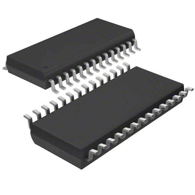
| 供应商器件封装 | 28-TSSOP |
| 信噪比 | Yes |
| 其它名称 | 296-18673-5 |
| 分辨率 | 24 bit |
| 制造商产品页 | http://www.ti.com/general/docs/suppproductinfo.tsp?distId=10&orderablePartNumber=ADS1234IPW |
| 包装 | 管件 |
| 单位重量 | 117.500 mg |
| 商标 | Texas Instruments |
| 安装类型 | 表面贴装 |
| 安装风格 | SMD/SMT |
| 封装 | Tube |
| 封装/外壳 | 28-TSSOP(0.173",4.40mm 宽) |
| 封装/箱体 | TSSOP-28 |
| 工作温度 | -40°C ~ 105°C |
| 工作电源电压 | 2.7 V to 5.3 V |
| 工厂包装数量 | 50 |
| 接口类型 | Serial SPI |
| 数据接口 | 串行 |
| 最大功率耗散 | 13.1 mW |
| 最大工作温度 | + 105 C |
| 最小工作温度 | - 40 C |
| 标准包装 | 50 |
| 特性 | PGA |
| 电压参考 | 5 V |
| 电压源 | 模拟和数字 |
| 系列 | ADS1234 |
| 结构 | Sigma-Delta |
| 视频文件 | http://www.digikey.cn/classic/video.aspx?PlayerID=1364138032001&width=640&height=455&videoID=44659313001 |
| 转换器数 | 1 |
| 转换器数量 | 1 |
| 转换速率 | 80 S/s |
| 输入数和类型 | 4 个单端,单极2 个差分,双极 |
| 输入类型 | Differential |
| 通道数量 | 4 Channel |
| 采样率(每秒) | 10,80 |


- 商务部:美国ITC正式对集成电路等产品启动337调查
- 曝三星4nm工艺存在良率问题 高通将骁龙8 Gen1或转产台积电
- 太阳诱电将投资9.5亿元在常州建新厂生产MLCC 预计2023年完工
- 英特尔发布欧洲新工厂建设计划 深化IDM 2.0 战略
- 台积电先进制程称霸业界 有大客户加持明年业绩稳了
- 达到5530亿美元!SIA预计今年全球半导体销售额将创下新高
- 英特尔拟将自动驾驶子公司Mobileye上市 估值或超500亿美元
- 三星加码芯片和SET,合并消费电子和移动部门,撤换高东真等 CEO
- 三星电子宣布重大人事变动 还合并消费电子和移动部门
- 海关总署:前11个月进口集成电路产品价值2.52万亿元 增长14.8%


PDF Datasheet 数据手册内容提取
ADS1232 ADS1234 www.ti.com SBAS350F–JUNE2005–REVISEDFEBRUARY2008 24-Bit Analog-to-Digital Converter For Bridge Sensors FEATURES DESCRIPTION 1 • CompleteFront-EndforBridgeSensors The ADS1232 and ADS1234 are precision 24-bit 2 • Upto23.5EffectiveBits analog-to-digital converters (ADCs). With an onboard, • Onboard,Low-NoisePGA low-noise programmable gain amplifier (PGA), precision delta-sigma ADC and internal oscillator, the • RMSNoise: ADS1232/4 provide a complete front-end solution for 17nVat10SPS(PGA=128) bridge sensor applications including weigh scales, 44nVat80SPS(PGA=128) straingaugesandpressuresensors. • 19.2-BitNoise-FreeResolutionatGain=64 The input multiplexer accepts either two (ADS1232) • Over100dBSimultaneous50Hzand60Hz or four (ADS1234) differential inputs. The ADS1232 Rejection also includes an onboard temperature sensor to • FlexibleClocking: monitorambient temperature. The onboard, low-noise PGA has a selectable gain of 1, 2, 64, or 128 Low-DriftOnboardOscillator(±3%) supporting a full-scale differential input of ±2.5V, OptionalExternalCrystal ±1.25V, ±39mV, or ±19.5mV. The delta-sigma ADC • SelectableGainsof1,2,64,and128 has 23.5-bit effective resolution and is comprised of a • EasyRatiometricMeasurements– 3rd-order modulator and 4th-order digital filter. Two ExternalVoltageReferenceupto5V data rates are supported: 10SPS (with both 50Hz and 60Hz rejection) and 80SPS. The ADS1232/4 can be • Selectable10SPSor80SPSDataRates clocked externally using an oscillator or a crystal. • Two-ChannelDifferentialInputwithBuilt-In There is also an internal oscillator available that TemperatureSensor(ADS1232) requires no external components. Offset calibration is • Four-ChannelDifferentialInput(ADS1234) performed on-demand and the ADS1232/4 can be put in a low-power standby mode or shut off • SimpleSerialDigitalInterface completelyinpower-downmode.Allof the features of • SupplyRange:2.7Vto5.3V the ADS1232/4 are operated through simple • –40(cid:176) Cto+105(cid:176) CTemperatureRange pin-driven control. There are no digital registers to program in order to simplify software development. APPLICATIONS Data are output over an easily-isolated serial interface that connects directly to the MSP430 and • WeighScales othermicrocontrollers. • StrainGauges The ADS1232 is available in a TSSOP-24 package • PressureSensors and the ADS1234 is in a TSSOP-28. Both are fully • IndustrialProcessControl specifiedfrom-40(cid:176) Cto+105(cid:176) C. AVDD CAP REFP REFN DVDD Gain = GAIN [1:0] AINP1 1, 2, 64, or 128 AINN1 PDWN AINP2 DRDY/DOUT AINN2 Input PGA DSADC Mux SCLK AINP3 ADS1234 AINN3 Internal Oscillator Only AINP4 SPEED External Oscillator AINN4 (1) A1/TEMP A0 AGND CAP CLKIN/XTAL1 XTAL2 DGND NOTE: (1) A1 for ADS1234, TEMP for ADS1232. 1 Pleasebeawarethatanimportantnoticeconcerningavailability,standardwarranty,anduseincriticalapplicationsof TexasInstrumentssemiconductorproductsanddisclaimerstheretoappearsattheendofthisdatasheet. Alltrademarksarethepropertyoftheirrespectiveowners. 2 PRODUCTIONDATAinformationiscurrentasofpublicationdate. Copyright©2005–2008,TexasInstrumentsIncorporated Products conform to specifications per the terms of the Texas Instruments standard warranty. Production processing does not necessarilyincludetestingofallparameters.
ADS1232 ADS1234 www.ti.com SBAS350F–JUNE2005–REVISEDFEBRUARY2008 This integrated circuit can be damaged by ESD. Texas Instruments recommends that all integrated circuits be handled with appropriateprecautions.Failuretoobserveproperhandlingandinstallationprocedurescancausedamage. ESDdamagecanrangefromsubtleperformancedegradationtocompletedevicefailure.Precisionintegratedcircuitsmaybemore susceptibletodamagebecauseverysmallparametricchangescouldcausethedevicenottomeetitspublishedspecifications. ORDERING INFORMATION For the most current package and ordering information, see the Package Option Addendum at the end of this datasheet,orseetheTIwebsiteatwww.ti.com. ABSOLUTE MAXIMUM RATINGS overoperatingfree-airtemperaturerange(unlessotherwisenoted)(1) ADS1232,ADS1234 UNIT AVDDtoAGND –0.3to+6 V DVDDtoDGND –0.3to+6 V AGNDtoDGND –0.3to+0.3 V InputCurrent 100,Momentary mA InputCurrent 10,Continuous mA AnalogInputVoltagetoAGND –0.3toAVDD+0.3 V DigitalInputVoltagetoDGND –0.3toDVDD+0.3 V MaximumJunctionTemperature +150 (cid:176) C OperatingTemperatureRange –40to+105 (cid:176) C StorageTemperatureRange –60to+150 (cid:176) C (1) StressesbeyondthoselistedunderAbsoluteMaximumRatingsmaycausepermanentdamagetothedevice.Thesearestressratings only,andfunctionaloperationofthedeviceattheseoranyotherconditionsbeyondthoseindicatedunderRecommendedOperating Conditionsisnotimplied.Exposuretoabsolute-maximum-ratedconditionsforextendedperiodsmayaffectdevicereliability. 2 Copyright©2005–2008,TexasInstrumentsIncorporated ProductFolderLink(s):ADS1232ADS1234
ADS1232 ADS1234 www.ti.com SBAS350F–JUNE2005–REVISEDFEBRUARY2008 ELECTRICAL CHARACTERISTICS AllspecificationsatT =–40(cid:176) Cto+105(cid:176) C,AVDD=DVDD=VREFP=+5V,andVREFN=AGND,unlessotherwisenoted. A ADS1232,ADS1234 PARAMETER CONDITIONS MIN TYP MAX UNIT AnalogInputs Full-ScaleInputVoltage (AINP–AINN) ±0.5VREF/Gain V AINxPorAINxNwithrespecttoGND, AGND–0.1 AVDD+0.1 V Common-ModeInputRange Gain=1,2 Gain=64,128 AGND+1.5V AVDD–1.5V V Gain=1 ±3 nA DifferentialInputCurrent Gain=2 ±6 nA Gain=64,128 ±3.5 nA SystemPerformance Resolution NoMissingCodes 24 Bits InternalOscillator,SPEED=High 78 80 82.4 SPS InternalOscillator,SPEED=Low 9.75 10 10.3 SPS DataRate ExternalOscillator,SPEED=High fCLK/61,440 SPS ExternalOscillator,SPEED=Low fCLK/491,520 SPS DigitalFilterSettlingTime FullSettling 4 Conversions DifferentialInput,End-PointFit ±0.0002 ±0.001 %ofFSR(1) Gain=1,2 IntegralNonlinearity(INL) DifferentialInput,End-PointFit ±0.0004 %ofFSR Gain=64,128 Gain=1 ±0.2 ±5 ppmofFS InputOffsetError(2) Gain=128 ±0.02 ±1 ppmofFS Gain=1 ±0.3 µV/(cid:176)C InputOffsetDrift Gain=128 ±10 nV/(cid:176)C Gain=1 ±0.001 ±0.02 % GainError(3) Gain=128 ±0.01 ±0.1 % Gain=1 ±0.2 ppm/(cid:176)C GainDrift Gain=128 ±2.5 ppm/(cid:176)C InternalOscillator,fDATA=10SPS 100 110 dB Normal-ModeRejection(4) fIN=50Hzor60Hz,±1Hz ExternalOscillator,fDATA=10SPS 120 130 dB fIN=50Hzor60Hz,±1Hz atDC,Gain=1,ΔV=1V 95 110 dB Common-ModeRejection atDC,Gain=128,ΔV=0.1V 95 110 dB Input-ReferredNoise SeeNoisePerformanceTables atDC,Gain=1,ΔV=1V 100 120 dB Power-SupplyRejection atDC,Gain=128,ΔV=0.1V 100 120 dB VoltageReferenceInput VoltageReferenceInput(VREF) VREF=VREFP–VREFN 1.5 AVDD AVDD+0.1V V NegativeReferenceInput(VREFN) AGND–0.1 VREFP–1.5 V PositiveReferenceInput(VREFP) VREFN+1.5 AVDD+0.1 V VoltageReference 10 nA InputCurrent (1) FSR=full-scalerange=V /Gain. REF (2) Offsetcalibrationcanminimizetheseerrorstothelevelofnoiseatanytemperature. (3) Gainerrorsarecalibratedatthefactory(AVDD=+5V,allgains,T =+25(cid:176) C). A (4) Specificationisassuredbythecombinationofdesignandfinalproductiontest. Copyright©2005–2008,TexasInstrumentsIncorporated 3 ProductFolderLink(s):ADS1232ADS1234
ADS1232 ADS1234 www.ti.com SBAS350F–JUNE2005–REVISEDFEBRUARY2008 ELECTRICAL CHARACTERISTICS (continued) AllspecificationsatT =–40(cid:176) Cto+105(cid:176) C,AVDD=DVDD=VREFP=+5V,andVREFN=AGND,unlessotherwisenoted. A ADS1232,ADS1234 PARAMETER CONDITIONS MIN TYP MAX UNIT Digital LogicLevels VIH 0.7DVDD DVDD+0.1 V VIL DGND 0.2DVDD V VOH IOH=1mA DVDD–0.4 V VOL IOL=1mA 0.2DVDD V InputLeakage 0<VIN<DVDD ±10 m A ExternalClockInputFrequency 0.2 4.9152 8 MHz (fCLKIN) SerialClockInputFrequency(fSCLK) 5 MHz PowerSupply Power-SupplyVoltage 2.7 5.3 V (AVDD,DVDD) NormalMode,AVDD=3V, 600 1300 m A Gain=1,2 NormalMode,AVDD=3V, 1350 2500 m A Gain=64,128 AnalogSupplyCurrent NGoarinm=al1M,o2de,AVDD=5V, 650 1300 m A NormalMode,AVDD=5V, 1350 2500 m A Gain=64,128 StandbyMode 0.1 1 m A Power-Down 0.1 1 µA NormalMode,DVDD=3V, 60 95 µA Gain=1,2 NormalMode,DVDD=3V, 75 120 µA Gain=64,128 NormalMode,DVDD=5V, 95 130 µA Gain=1,2 DigitalSupplyCurrent Normalmode,DVDD=5V, 75 120 µA Gain=64,128 StandbyMode,SCLK=High,DVDD=3V 45 80 µA StandbyMode,SCLK=High,DVDD=5V 65 80 m A Power-Down 0.2 1.3 µA NormalMode,AVDD=DVDD=3V, 2 4.2 mW Gain=1,2 NormalMode,AVDD=DVDD=5V, 3.7 7.2 mW Gain=1,2 PowerDissipation,Total NormalMode,AVDD=DVDD=3V, 4.3 7.9 mW Gain=64,128 NormalMode,AVDD=DVDD=5V, 7.1 13.1 mW Gain=64,128 StandbyMode,AVDD=DVDD=5V 0.3 0.4 mW 4 Copyright©2005–2008,TexasInstrumentsIncorporated ProductFolderLink(s):ADS1232ADS1234
ADS1232 ADS1234 www.ti.com SBAS350F–JUNE2005–REVISEDFEBRUARY2008 NOISE PERFORMANCE The ADS1232/4 offer outstanding noise performance that can be optimized for a given full-scale range using the on-chip programmable gain amplifier. Table 1 through Table 4 summarize the typical noise performance with inputsshortedexternallyfordifferentgains,datarates,andvoltagereferencevalues. TheRMSandPeak-to-Peaknoisearereferredtotheinput.TheEffectiveNumberofBits(ENOB)isdefinedas: • ENOB=ln(FSR/RMSnoise)/ln(2) TheNoise-FreeBitsaredefinedas: • Noise-FreeBits=ln(FSR/Peak-to-PeakNoise)/ln(2) WhereFSR(Full-ScaleRange)=V /Gain REF Table1.AVDD=5V,V =5V,DataRate=10SPS REF GAIN RMSNOISE PEAK-TO-PEAKNOISE(1) ENOB(RMS) NOISE-FREEBITS 1 420nV 1.79µV 23.5 21.4 2 270nV 900nV 23.1 21.4 64 19nV 125nV 22.0 19.2 128 17nV 110nV 21.1 18.4 (1) Peak-to-peaknoisedataarebasedondirectmeasurement. Table2.AVDD=5V,V =5V,DataRate=80SPS REF GAIN RMSNOISE PEAK-TO-PEAKNOISE(1) ENOB(RMS) NOISE-FREEBITS 1 1.36µV 8.3µV 21.8 19.2 2 850nV 5.5µV 21.5 18.8 64 48nV 307nV 20.6 18 128 44nV 247nV 19.7 17.2 (1) Peak-to-peaknoisedataarebasedondirectmeasurement. Table3.AVDD=3V,V =3V,DataRate=10SPS REF GAIN RMSNOISE PEAK-TO-PEAKNOISE(1) ENOB(RMS) NOISE-FREEBITS 1 450nV 2.8µV 22.6 20 2 325nV 1.8µV 22.1 19.7 64 20nV 130nV 21.2 18.5 128 18nV 115nV 20.3 17.6 (1) Peak-to-peaknoisedataarebasedondirectmeasurement. Table4.AVDD=3V,V =3V,DataRate=80SPS REF GAIN RMSNOISE PEAK-TO-PEAKNOISE(1) ENOB(RMS) NOISE-FREEBITS 1 2.2µV 12µV 20.4 17.9 2 1.2µV 6.8µV 20.2 17.8 64 54nV 340nV 19.7 17.1 128 48nV 254nV 18.9 16.5 (1) Peak-to-peaknoisedataarebasedondirectmeasurementof1024samples. Copyright©2005–2008,TexasInstrumentsIncorporated 5 ProductFolderLink(s):ADS1232ADS1234
ADS1232 ADS1234 www.ti.com SBAS350F–JUNE2005–REVISEDFEBRUARY2008 PIN CONFIGURATION DVDD 1 28 DRDY/DOUT DVDD 1 24 DRDY/DOUT DGND 2 27 SCLK DGND 2 23 SCLK CLKIN/XTAL1 3 26 PDWN CLKIN/XTAL1 3 22 PDWN XTAL2 4 25 SPEED XTAL2 4 21 SPEED DGND 5 24 GAIN1 DGND 5 20 GAIN1 DGND 6 23 GAIN0 DGND 6 19 GAIN0 A1 7 22 AVDD ADS1232 ADS1234 TEMP 7 18 AVDD A0 8 21 AGND A0 8 17 AGND CAP 9 20 REFP CAP 9 16 REFP CAP 10 19 REFN CAP 10 15 REFN AINP1 11 18 AINP2 AINP1 11 14 AINP2 AINN1 12 17 AINN2 AINN1 12 13 AINN2 AINP3 13 16 AINP4 AINN3 14 15 AINN4 6 Copyright©2005–2008,TexasInstrumentsIncorporated ProductFolderLink(s):ADS1232ADS1234
ADS1232 ADS1234 www.ti.com SBAS350F–JUNE2005–REVISEDFEBRUARY2008 PINDESCRIPTIONS TERMINAL ANALOG/DIGITAL NAME ADS1232 ADS1234 INPUT/OUTPUT DESCRIPTION DVDD 1 1 Digital DigitalPowerSupply:2.7Vto5.3V DGND 2 2 Digital DigitalGround CLKIN/ ExternalClockInput:typically4.9152MHz.Tielowtoactivateinternaloscillator.Canalsouse 3 3 Digital/DigitalInput XTAL1 externalcrystalacrossCLKIN/XTAL1andXTAL2pins.Seetextformoredetails. XTAL2 4 4 Digital Externalcrystalconnection DGND 5 5 Digital DigitalGround DGND 6 6 Digital DigitalGround TEMP 7 – DigitalInput OnboardTemperatureDiodeEnable InputMuxSelectInputpin(MSB) InputMuxSelectInputpin(LSB): A1 A0 Channel A1 – 7 DigitalInput 0 0 AIN1 A0 8 8 0 1 AIN2 1 0 AIN3 1 1 AIN4 CAP 9 9 Analog GainAmpBypassCapacitorConnection CAP 10 10 Analog GainAmpBypassCapacitorConnection AINP1 11 11 AnalogInput PositiveAnalogInputChannel1 AINN1 12 12 AnalogInput NegativeAnalogInputChannel1 AINP3 – 13 AnalogInput PositiveAnalogInputChannel3 AINN3 – 14 AnalogInput NegativeAnalogInputChannel3 AINN4 – 15 AnalogInput NegativeAnalogInputChannel4 AINP4 – 16 AnalogInput PositiveAnalogInputChannel4 AINN2 13 17 AnalogInput NegativeAnalogInputChannel2 AINP2 14 18 AnalogInput PositiveAnalogInputChannel2 REFN 15 19 AnalogInput NegativeReferenceInput REFP 16 20 AnalogInput PositiveReferenceInput AGND 17 21 Analog AnalogGround AVDD 18 22 Analog AnalogPowerSupply,2.7Vto5.3V GainSelect GAIN1 GAIN0 GAIN GAIN0 19 23 0 0 1 DigitalInput GAIN1 20 24 0 1 2 1 0 64 1 1 128 DataRateSelect: SPEED DATARATE SPEED 21 25 DigitalInput 0 10SPS 1 80SPS PDWN 22 26 DigitalInput Power-Down:HoldingthispinlowpowersdowntheentireconverterandresetstheADC. SerialClock:Clockoutdataontherisingedge.AlsousedtoinitiateOffsetCalibrationandSleep SCLK 23 27 DigitalInput modes.Seetextformoredetails. Dual-PurposeOutput: DRDY/ 24 28 DigitalOutput DataReady:Indicatesvaliddatabygoinglow. DOUT DataOutput:Outputsdata,MSBfirst,onthefirstrisingedgeofSCLK. Copyright©2005–2008,TexasInstrumentsIncorporated 7 ProductFolderLink(s):ADS1232ADS1234
ADS1232 ADS1234 www.ti.com SBAS350F–JUNE2005–REVISEDFEBRUARY2008 TYPICAL CHARACTERISTICS AtT =+25(cid:176) C,AVDD=DVDD=VREFP=5V,andVREFN=AGND,unlessotherwisenoted. A NOISEPLOT NOISEPLOT 6 25 PGA=1 5 DataRate=10SPS 20 4 15 B) 3 B) 10 S S (L 2 (L 5 de 1 de o o 0 C - 1 C put - 2 put - 5 Out - 3 Out- 10 - 4 - 15 - 5 - 20 PGA=128 DataRate=10SPS - 6 - 25 0 200 400 600 800 1000 0 200 400 600 800 1000 Time(ReadingNumber) Time(ReadingNumber) Figure1. Figure2. NOISEHISTOGRAM NOISEHISTOGRAM 300 100 PGA=1 PGA=128 DataRate=10SPS 90 DataRate=10SPS 250 80 70 200 ce ce 60 n n e e urr 150 urr 50 c c Oc Oc 40 100 30 20 50 10 0 0 - 4 - 2 0 2 4 - 16 - 8 0 8 16 OutputCode(LSB) OutputCode(LSB) Figure3. Figure4. NOISEPLOT NOISEPLOT 22.5 70 PGA=128 PGA=1 17.5 DataRate=80SPS DataRate=80SPS 50 12.5 B) B) 30 S 7.5 S de(L 2.5 de(L 10 o o utC - 2.5 utC - 10 p p Out - 7.5 Out - 30 - 12.5 - 50 - 17.5 - 22.5 - 70 0 200 400 600 800 1000 0 200 400 600 800 1000 Time(ReadingNumber) Time(ReadingNumber) Figure5. Figure6. 8 Copyright©2005–2008,TexasInstrumentsIncorporated ProductFolderLink(s):ADS1232ADS1234
ADS1232 ADS1234 www.ti.com SBAS350F–JUNE2005–REVISEDFEBRUARY2008 TYPICAL CHARACTERISTICS (continued) AtT =+25(cid:176) C,AVDD=DVDD=VREFP=5V,andVREFN=AGND,unlessotherwisenoted. A NOISEHISTOGRAM NOISEHISTOGRAM 180 50 PGA=1 PGA=128 160 DataRate=80SPS 45 DataRate=80SPS 40 140 35 120 ce ce 30 n 100 n a a ur ur 25 Occ 80 Occ 20 60 15 40 10 20 5 0 0 - 12 - 6 0 6 12 - 40 - 20 0 20 40 OutputCode(LSB) OutputCode(LSB) Figure7. Figure8. OFFSETDRIFT(–40(cid:176) Cto+25(cid:176) C) OFFSETDRIFT(+25(cid:176) Cto+105(cid:176) C) 35 35 PGA = 1 PGA = 1 30 Data Rate = 10SPS 30 Data Rate = 10SPS 90 Samples from 3 Lots 90 Samples from 3 Lots 25 25 nts 20 nts 20 u u Co 15 Co 15 10 10 5 5 0 0 0 0 0 0 0 0 0 0 0 0 0 0 0 0 0 0 0 0 0 0 0 0 0 0 0 0 0 0 0 0 0 0 0 0 0 0 0 0 0 0 0 0 0 0 0 0 6 5 4 3 2 1 1 2 3 4 5 6 5 4 3 2 1 1 2 3 4 5 - - - - - - - - - - - Offset Drift (nV/°C) Offset Drift (nV/°C) Figure9. Figure10. GAINDRIFT(–40(cid:176) Cto+25(cid:176) C) GAINDRIFT(+25(cid:176) Cto+105(cid:176) C) 18 20 PGA = 1 PGA = 1 16 Data Rate = 10SPS 18 Data Rate = 10SPS 14 90 Samples from 3 Lots 16 90 Samples from 3 Lots 14 12 12 s 10 s unt unt 10 Co 8 Co 8 6 6 4 4 2 2 0 0 2109876543210123456789012 098765432101234567890 1.1.1.0.0.0.0.0.0.0.0.0. 0.0.0.0.0.0.0.0.0.1.1.1. 1.0.0.0.0.0.0.0.0.0. 0.0.0.0.0.0.0.0.0.1. ------------ ---------- Gain Drift (ppm/°C) Gain Drift (ppm/°C) Figure11. Figure12. Copyright©2005–2008,TexasInstrumentsIncorporated 9 ProductFolderLink(s):ADS1232ADS1234
ADS1232 ADS1234 www.ti.com SBAS350F–JUNE2005–REVISEDFEBRUARY2008 TYPICAL CHARACTERISTICS (continued) AtT =+25(cid:176) C,AVDD=DVDD=VREFP=5V,andVREFN=AGND,unlessotherwisenoted. A OFFSETDRIFT(–40(cid:176) Cto+25(cid:176) C) OFFSETDRIFT(+25(cid:176) Cto+105(cid:176) C) 30 20 PGA = 128 PGA = 128 Data Rate = 10SPS 18 Data Rate = 10SPS 25 90 Samples from 3 Lots 16 90 Samples from 3 Lots 14 20 12 Counts 15 Counts 108 10 6 4 5 2 0 0 0 0 0 0 0 0 0 0 0 0 0 0 5 0 5 0 5 0 5 0 5 0 5 0 5 4 3 2 1 1 2 3 4 5 3 2 2 1 1 - 1 1 2 2 3 - - - - - - - - - - Offset Drift (nV/°C) Offset Drift (nV/°C) Figure13. Figure14. GAINDRIFT(–40(cid:176) Cto+25(cid:176) C) GAINDRIFT(+25(cid:176) Cto+105(cid:176) C) 25 20 PGA = 128 PGA = 128 18 Data Rate = 10SPS Data Rate = 10SPS 20 90 Samples from 3 Lots 16 90 Samples from 3 Lots 14 15 12 unts unts 10 o o C 10 C 8 6 5 4 2 0 0 0 5 0 5 0 5 0 5 0 5 0 0 5 0 5 0 5 0 5 0 5 0 5 0 0. 1. 1. 2. 2. 3. 3. 4. 4. 5. 0. 1. 1. 2. 2. 3. 3. 4. 4. 5. 5. 6. Gain Drift (ppm/°C) Gain Drift (ppm/°C) Figure15. Figure16. OFFSETvsTEMPERATURE GAINERRORvsTEMPERATURE 1000 0.04 PGA=128 PGA=128 DataRate=10SPS DataRate=10SPS 0.03 500 %)0.02 V) ( et(n 0 Error0.01 s Off ain G 0 - 500 - 0.01 - 1000 - 0.02 - 50 - 30 - 10 10 30 50 70 90 110 - 50 - 30 - 10 10 30 50 70 90 110 Temperature((cid:1)C) Temperature((cid:1)C) Figure17. Figure18. 10 Copyright©2005–2008,TexasInstrumentsIncorporated ProductFolderLink(s):ADS1232ADS1234
ADS1232 ADS1234 www.ti.com SBAS350F–JUNE2005–REVISEDFEBRUARY2008 TYPICAL CHARACTERISTICS (continued) AtT =+25(cid:176) C,AVDD=DVDD=VREFP=5V,andVREFN=AGND,unlessotherwisenoted. A NOISEvsINPUTSIGNAL NOISEvsINPUTSIGNAL 1000 50 PGA=1 PGA=128 900 45 DataRate=10SPS DataRate=10SPS 800 40 700 35 V) V) (n 600 (n 30 e e ois 500 ois 25 N N S 400 S 20 M M R 300 R 15 200 10 100 5 0 0 - 2.5 - 2.0 - 1.5 - 1.0 - 0.5 0 0.5 1.0 1.5 2.0 2.5 - 19 - 14.25 - 9.5 - 4.75 0 4.75 9.5 14.25 19 V (V) V (mV) IN IN Figure19. Figure20. INTEGRALNONLINEARITY INTEGRALNONLINEARITY vsINPUTSIGNAL vsINPUTSIGNAL 5 25 10 390.625 PGA=1 PGA=128 4 20 8 312.5 3 15 6 234.375 R) 2 10 R) 4 156.25 mofFS 10 50 m(V) mofFS 20 708.125 (nV) (pp - 1 - 5 INL (pp- 2 - 78.125INL L L IN - 2 - 10 IN- 4 - 156.25 - 3 - 15 - 6 - 234.375 - 4 - 20 - 8 - 312.5 - 5 - 25 - 10 - 390.625 - 2.5 - 2.0 - 1.5 - 1.0 - 0.5 0 0.5 1.0 1.5 2.0 2.5 - 19 - 14.25 - 9.5 - 4.75 0 4.75 9.5 14.25 19 V (V) V (mV) IN IN Figure21. Figure22. ANALOGCURRENT DIGITALCURRENT vsTEMPERATURE vsTEMPERATURE 2000 120 NormalMode,PGA=64,128 NormalMode,PGA=1,2 100 1600 A) A) NormalMode,PGA=64,128 80 mCurrent( 1200 NormalMode,PGA=1,2 mCurrent( 60 SleepMode,AllPGAs alog 800 gital 40 An Di 400 20 0 0 - 50 - 30 - 10 10 30 50 70 90 110 - 50 - 30 - 10 10 30 50 70 90 110 Temperature((cid:1)C) Temperature((cid:1)C) Figure23. Figure24. Copyright©2005–2008,TexasInstrumentsIncorporated 11 ProductFolderLink(s):ADS1232ADS1234
ADS1232 ADS1234 www.ti.com SBAS350F–JUNE2005–REVISEDFEBRUARY2008 TYPICAL CHARACTERISTICS (continued) AtT =+25(cid:176) C,AVDD=DVDD=VREFP=5V,andVREFN=AGND,unlessotherwisenoted. A DATARATE vsTEMPERATURE 10.06 SPEED=LOW CLKIN/XTAL1=LOW(InternalOscillator) 10.01 S) P S ( ate 9.96 R a at D 9.91 9.86 - 50 - 30 - 10 10 30 50 70 90 110 Temperature((cid:1)C) Figure25. 12 Copyright©2005–2008,TexasInstrumentsIncorporated ProductFolderLink(s):ADS1232ADS1234
ADS1232 ADS1234 www.ti.com SBAS350F–JUNE2005–REVISEDFEBRUARY2008 OVERVIEW TEMPERATURE SENSOR (ADS1232 only) The ADS1232 and ADS1234 are highly integrated, On-chip diodes provide temperature-sensing 24-bit ADCs that include an input multiplexer, capability. By setting the TEMP pin high, the selected low-noise PGA, third-order delta-sigma (ΔΣ) analog inputs are disconnected and the inputs to the modulator, and fourth-order digital filter. With ADC are connected to the anodes of two diodes input-referred RMS noise down to 17nV, the scaled to 1x and 80x in current and size, as shown in ADS1232/4 are ideally suited for measuring the very Figure 26. By measuring the difference in voltage of low signals produced by bridge sensors in these diodes, temperature changes can be inferred applicationssuchas weigh scales, strain gauges, and from a baseline temperature. Typically, the difference pressuresensors. in diode voltage is 111.7mV at 25(cid:176) C with a temperature coefficient of 379m V/(cid:176) C. With PGA = 1 Clocking can be supplied by an external oscillator, an and 2, the difference voltage output from the PGA will external crystal, or by a precision internal oscillator. be 111.7mV and 223.4mV, respectively. With PGA = Data can be output at 10SPS for excellent 50Hz and 64 and 128, it is impossible to use the temperature 60Hz rejection, or at 80SPS when higher speeds are sensor function. A similar structure is used in the needed. The ADS1232/4 are easy to configure, and MSC1210 for temperature measurement. For more all digital control is accomplished through dedicated information, see TI application report SBAA100, pins; there are no registers to program. A simple Using the MSC121x as a High-Precision Intelligent two-wireserialinterfaceretrievesthedata. Temperature Sensor, available for download at www.ti.com. ANALOG INPUTS (AINPx, AINNx) The input signal to be measured is applied to the input pins AINPx and AINNx. The positive internal input is generalized as AINP, and the negative ADS1232Only internal input generalized as AINN. The signal is selected through the input mux, which is controlled by AVDD pins A0 and A1 (ADS1234 only), as shown in Table 5. For the ADS1232, the A1 pin is replaced by 10I 1I the TEMP pin to activate the onboard diodes (see the Temperature Sensor section for more details). The AINP ADS1232/4 accept differential input signals, but can AINN also measure unipolar signals. When measuring unipolar (or single-ended signals) with respect to 1X 8X ground, connect the negative input (AINNx) to ground and connect the input signal to the positive input (AINPx). Note that when the ADS1232/4 are configured this way, only half of the converter full-scale range is used, since only positive digital AINP1 outputcodesareproduced. AINN1 AINP2 Table5.InputChannelSelectionwithA0andA1 AINN2 (ADS1234only) AINP3 MUXPINS SELECTEDANALOGINPUTS AINN3 A1 A0 POSITIVEINPUT NEGATIVEINPUT AINP4 0 0 AINP1 AINN1 AINN4 0 1 AINP2 AINN2 1 0 AINP3 AINN3 ADS1234Only A1 A0 1 1 AINP4 AINN3 Figure26.MeasurementoftheTemperature SensorintheInputMultiplexer Copyright©2005–2008,TexasInstrumentsIncorporated 13 ProductFolderLink(s):ADS1232ADS1234
ADS1232 ADS1234 www.ti.com SBAS350F–JUNE2005–REVISEDFEBRUARY2008 LOW-NOISE PGA BypassCapacitor The ADS1232/4 features a low-drift, low-noise PGA By applying a 0.1µF external capacitor (C ) across EXT that provides a complete front-end solution for bridge two capacitor pins and the combination of the internal sensors. A simplified diagram of the PGA is shown in 2kΩ resistor R on-chip, a low-pass filter (with a INT Figure 27. It consists of two chopper-stabilized cornerfrequencyof720Hz)iscreated to bandlimit the amplifiers (A1 and A2) and three accurately-matched signal path prior to the modulator input. This low-pass resistors (R , R , and R ), which construct a filter serves two purposes. First, the input signal is 1 F1 F2 differential front-end stage with a gain of 64, followed bandlimited to prevent aliasing as well as to filter out by gain stage A3. The PGA inputs are equipped with the high-frequency noise. Second, it attenuates the an EMI filter, as shown in Figure 27. The cut-off chopping residue from the PGA (for gains of 64 and frequency of the EMI filter is 19.6MHz. If the PGA is 128 only) to improve temperature drift performance. It set to 1 or 2, the gain-of-64 stage is bypassed and is not required to use high quality capacitors (such as shut down to save power. With the combination of ceramic or tantalum capacitors) for a general both gain stages, the PGA can be set to 64 or 128. application. However, high quality capacitors such as The PGA of the ADS1232/4 can be set to 1, 2, 64, or polyarerecommendedforhighlinearityapplications. 128 with pins GAIN1 (MSB) and GAIN0 (LSB). By using AVDD as the reference input, the bipolar input VOLTAGE REFERENCE INPUTS ranges from ±2.5V to ±19.5mV, while the unipolar (REFP, REFN) ranges from 2.5V to 19.5mV. When the PGA is set to The voltage reference used by the modulator is 1 or 2, the absolute inputs can go rail-to-rail without generated from the voltage difference between REFP significant performance degradation. However, the and REFN: V = REFP – REFN. The reference inputs of the ADS1232/4 are protected with internal REF inputs use a structure similar to that of the analog diodes connected to the power-supply rails. These inputs. In order to increase the reference input diodes will clamp the applied signal to prevent it from impedance, a switching buffer circuitry is used to damagingtheinputcircuitry.Onthe other hand, when reduce the input equivalent capacitance. The thePGAissetto 64 or 128, the operating input range reference drift and noise impact ADC performance. In is limited to (AGND + 1.5V) to (AVDD – 1.5V), in order to achieve best results, pay close attention to order to prevent saturating the differential front-end the reference noise and drift specifications. A circuitryanddegradingperformance. simplified diagram of the circuitry on the reference inputs is shown in Figure 28. The switches and CAP capacitors can be modeled with an effective 450W impedanceof: AINP 18pF A1 RINT Z (cid:1) 1 EFF 2f C MOD BUF R Gain of 1 or 2 F1 Where: f =modulatorsamplingfrequency(76.8kHz) R A3 ADC MOD 1 R F2 C =inputcapacitanceofthebuffer BUF FortheADS1232/4: R INT 450W A2 AINN 18pF CAP Figure27.SimplifiedDiagramofthePGA 14 Copyright©2005–2008,TexasInstrumentsIncorporated ProductFolderLink(s):ADS1232ADS1234
ADS1232 ADS1234 www.ti.com SBAS350F–JUNE2005–REVISEDFEBRUARY2008 Z (cid:1) 1 (cid:1)500M(cid:1) EFF (2)(76.8kHz)(13fF) Crystal Oscillator CLKIN/XTAL1 CLK_DETECT VREFP VREFN Internal EN Oscillator XTAL2 S0 S1 S MUX AVDD AVDD To ADC ESD Protection CBUF Z =500MW (1) Figure29.EquivalentCircuitryoftheClock EFF Source When the clock source is a crystal, simply connect the 4.9152MHz crystal across the CLKIN/XTAL1 and XTAL2 pins. Table 6 shows the recommended part (1)f =76.8kHz MOD numbers. Due to the low-power design of the parallel resonant driver circuitry onboard, both the Figure28.SimplifiedReferenceInputCircuitry CLKIN/XTAL1 and XTAL2 pins are only for use with external crystals; they should not be used as clock ESD diodes protect the reference inputs. To prevent output drivers for external circuitry. No external these diodes from turning on, make sure the voltages capacitors are used with the crystal; it is on the reference pins do not go below GND by more recommended to place the crystal close to the part in than 100mV, and likewise, do not exceed AVDD by order to reduce board stray capacitance for both the 100mV: CLKIN/XTAL1 and XTAL2 pins and to insure proper operation. GND–100mV<(REFPorREFN)<AVDD+100mV Table6.RecommendedCrystals CLOCK SOURCES MANUFACTURER FREQUENCY PARTNUMBER The ADS1232/4 can use an external clock source, ECS 4.9152MHz ECS-49-20-1 external crystal, or internal oscillator to accommodate ECS 4.9152MHz ECS-49-20-4 a wide variety of applications. Figure 29 shows the equivalent circuitry of the clock source. The CLK_DETECT block determines whether the crystal oscillator/external clock signal is applied to the An external oscillator may be used by driving the CLKIN/XTAL1 pin so that the internal oscillator is CLKIN/XTAL1 pin directly. The Electrical bypassed or activated. When the CLKIN/XTAL1 pin Characteristics table shows the allowable frequency frequency is above ~200kHz, the CLK_DETECT range. output goes low and shuts down the internal oscillator. When the XIN pin frequency is below ~200kHz, the CLK_DETECT output goes high and activates the internal oscillator. It is highly recommended to hard-wire the CLKIN/XTAL1 pin to groundwhentheinternaloscillatorischosen. Copyright©2005–2008,TexasInstrumentsIncorporated 15 ProductFolderLink(s):ADS1232ADS1234
ADS1232 ADS1234 www.ti.com SBAS350F–JUNE2005–REVISEDFEBRUARY2008 FREQUENCY RESPONSE Figure 31(b) shows the zoom in plot for both 50Hz and 60Hz notches with the SPEED pin tied low The ADS1232/4 use a sinc4 digital filter with the (10SPS data rate). With only a ±3% variation of the frequency response (f = 4.9152MHz) shown in CLK internal oscillator, over 100dB of normal-mode Figure 30. The frequency response repeats at rejectionisachieved. multiples of the modulator sampling frequency of 76.8kHz. The overall response is that of a low-pass filter with a –3dB cutoff frequency of 3.32Hz with the 0 DataRate=10SPS SPEED pin tied low (10SPS data rate) and 11.64Hz withtheSPEEDpintiedhigh(80SPSdatarate). - 50 B) d 0 ( n - 20 f =4.9152MHz Gai CLK - 100 - 40 - 60 dB) - 80 - 150 n( - 100 0 10 20 30 40 50 60 70 80 90 100 Gai - 120 Frequency(Hz) - 140 (a) - 160 - 50 - 180 DataRate=10SPS - 200 0 38.4 76.8 Frequency(kHz) B) d n( - 100 ai G Figure30.FrequencyResponse To help see the response at lower frequencies, Figure 31(a) illustrates the response out to 100Hz, - 150 when the data rate = 10SPS. Notice that signals at 46474849505152535455565758596061626364 multiples of 10Hz are rejected, and therefore Frequency(Hz) simultaneousrejectionof50Hzand60Hzisachieved. (b) The benefit of using a sinc4 filter is that every frequency notch has four zeros on the same location. Figure31.FrequencyResponseOutTo100Hz This response, combined with the low drift internal oscillator, provides an excellent normal-mode The ADS1232/4 data rate and frequency response rejectionofline-cycleinterference. scale directly with clock frequency. For example, if f increases from 4.9152MHz to 6.144MHz when CLK the SPEED pin is tied high, the data rate increases from 80SPS to 100SPS, while notches also increase from 80Hz to 100Hz. Note that this is only possible whentheexternalclocksourceisapplied. 16 Copyright©2005–2008,TexasInstrumentsIncorporated ProductFolderLink(s):ADS1232ADS1234
ADS1232 ADS1234 www.ti.com SBAS350F–JUNE2005–REVISEDFEBRUARY2008 SETTLING TIME switching input channels. Another example would be toggling the TEMP pin, which switches the internal After changing the input multiplexer, the first data are AINP, AINN signals to connect to either the external fully settled. In both the ADS1232/4, the digital filter is AINPx, AINNx pins or to the TEMP diode (see allowedtosettleaftertogglingeitherthe A1 or A0 pin. Figure26). Toggling any of these digital pins will hold the DRDY/DOUT line high until the digital filter is fully Note that when settling data, five readings may be settled. For example, if A0 changes from low to high, required. If the change in input occurs in the middle selecting a different input channel, DRDY/DOUT of the first conversion, four more full conversions of immediately goes high, and DRDY/DOUT goes low the fully-settled input are required to get fully-settled when fully-settled data are ready for retrieval. There data. Discard the first four readings because they is no need to discard any data. Figure 32 shows the contain only partially-settled data.Figure 33 illustrates timing of the DRDY/DOUT line as the input the settling time for the ADS1232/4 in Continuous multiplexerchanges. Conversionmode. In certain instances, large and/or abrupt changes in input will require four data cycles to settle. One example of such a change would be an external multiplexer in front of the ADS1232/4, which can cause large changes in input voltage simply by A1 or A0 t 1 DRDY/DOUT t S Figure32.ExampleofSettlingTimeAfterChangingtheInputMultiplexer SYMBOL DESCRIPTION(1) MIN MAX UNITS t SetuptimeforchangingtheA1orA0pins 40 50 m s S Settlingtime(DRDY/DOUT SPEED=1 51 51 ms t 1 heldhigh) SPEED=0 401 401 ms (1) Valuesgivenforf =4.9152MHz.Fordifferentf frequencies,scaleproportionaltoCLKperiod.Expecta±3%variationwhenan CLK CLK internaloscillatorisused. Toggled TEMP Pin orAbrupt Change in External V IN V IN 2nd conversion; 3rd conversion; 4th conversion; 5th conversion; Start of 1st conversion; VINsettled, but VINsettled, but VINsettled, but VINand digital conversion. includes digital filter digital filter digital filter filter both DRDY/DOUT unsettled VIN. unsettled. unsettled. unsettled. settled. Conversion Time Figure33.SettlingTimeinContinuousConversionMode Copyright©2005–2008,TexasInstrumentsIncorporated 17 ProductFolderLink(s):ADS1232ADS1234
ADS1232 ADS1234 www.ti.com SBAS350F–JUNE2005–REVISEDFEBRUARY2008 DATA RATE DATA READY/DATA OUTPUT (DRDY/DOUT) The ADS1232/4 data rate is set by the SPEED pin, This digital output pin serves two purposes. First, it as shown in Table 7. When SPEED is low, the data indicates when new data are ready by going low. rate is nominally 10SPS. This data rate provides the Afterwards, on the first rising edge of SCLK, the lowest noise, and also has excellent rejection of both DRDY/DOUT pin changes function and begins 50Hz and 60Hz line-cycle interference. For outputting the conversion data, most significant bit applications requiring fast data rates, setting SPEED (MSB) first. Data are shifted out on each subsequent highselectsadatarateofnominally80SPS. SCLK rising edge. After all 24 bits have been retrieved, the pin can be forced high with an Table7.DataRateSettings additional SCLK. It will then stay high until new data are ready. This configuration is useful when polling DATARATE on the status of DRDY/DOUT to determine when to SPEED InternalOscillator External begindataretrieval. PIN or4.9152MHzCrystal Oscillator 0 10SPS fCLKIN/491,520 SERIAL CLOCK INPUT (SCLK) 1 80SPS f /61,440 CLKIN This digital input shifts serial data out with each rising edge. This input has built-in hysteresis, but care DATA FORMAT shouldstillbetakentoensureacleansignal. Glitches The ADS1232/4 output 24 bits of data in binary two’s or slow-rising signals can cause unwanted additional complement format. The least significant bit (LSB) shifting. For this reason, it is best to make sure the has a weight of 0.5V /(223 – 1). The positive rise-and-falltimesofSCLKarelessthan50ns. REF full-scale input produces an output code of 7FFFFFh and the negative full-scale input produces an output code of 800000h. The output clips at these codes for signals exceeding full-scale. Table 8 summarizes the idealoutputcodesfordifferentinputsignals. Table8.IdealOutputCodevsInputSignal(1) INPUTSIGNALV IN (AINP–AINN) IDEALOUTPUTCODE ≥+0.5V /Gain 7FFFFFh REF (+0.5V /Gain)/(223–1) 000001h REF 0 000000h (–0.5V /Gain)/(223–1) FFFFFFh REF ≤–0.5V /Gain 800000h REF (1) Excludeseffectsofnoise,INL,offset,andgainerrors. 18 Copyright©2005–2008,TexasInstrumentsIncorporated ProductFolderLink(s):ADS1232ADS1234
ADS1232 ADS1234 www.ti.com SBAS350F–JUNE2005–REVISEDFEBRUARY2008 DATA RETRIEVAL indicating that new data are being updated. To avoid having DRDY/DOUT remain in the state of the last The ADS1232/4 continuously convert the analog bit, the user can shift SCLK to force DRDY/DOUT input signal. To retrieve data, wait until DRDY/DOUT high, as shown in Figure 35. This technique is useful goes low, as shown in Figure 34. After this occurs, when a host controlling the device is polling begin shifting out the data by applying SCLKs. Data DRDY/DOUTtodeterminewhendataareready. are shifted out MSB first. It is not required to shift out all 24 bits of data, but the data must be retrieved before new data are updated (within t ) or else it will 7 be overwritten. Avoid data retrieval during the update period (t ). DRDY/DOUT remains at the state of the 6 last bit shifted out until it is taken high (see t ), 6 Data DataReady NewDataReady MSB LSB DRDY/DOUT 23 22 21 0 t t 4 5 t t t 2 3 6 SCLK 1 24 t 3 t 7 Figure34.DataRetrievalTiming SYMBOL DESCRIPTION MIN TYP MAX UNITS t DRDY/DOUTlowtofirstSCLKrisingedge 0 ns 2 t SCLKpositiveornegativepulsewidth 100 ns 3 SCLKrisingedgetonewdatabitvalid:propagation t 50 ns 4 delay t SCLKrisingedgetoolddatabitvalid:holdtime 0 ns 5 t (1) Dataupdating:noreadbackallowed 39 m s 6 SPEED=1 12.5 ms t (1) Conversiontime(1/datarate) 7 SPEED=0 100 ms (1) Valuesgivenforf =4.9152MHz.Fordifferentf frequencies,scaleproportionaltoCLKperiod. CLK CLK Data DataReady NewDataReady DRDY/DOUT 23 22 21 0 SCLK 1 24 25 25thSCLKtoForceDRDY/DOUTHigh Figure35.DataRetrievalwithDRDY/DOUTForcedHighAfterwards Copyright©2005–2008,TexasInstrumentsIncorporated 19 ProductFolderLink(s):ADS1232ADS1234
ADS1232 ADS1234 www.ti.com SBAS350F–JUNE2005–REVISEDFEBRUARY2008 OFFSET CALIBRATION When the calibration is completed, DRDY/DOUT goes low, indicating that new data are ready. The Offset calibration can be initiated at any time to analog input pins are disconnected within the ADC remove the ADS1232/4 inherited offset error. To and the appropriate signal is applied internally to initiate offset calibration, apply at least two additional perform the calibration. The first conversion after a SCLKs after retrieving 24 bits of data. Figure 36 calibration is fully settled and valid for use. The offset shows the timing pattern. The 25th SCLK will send calibrationtakesexactlythesametime as specified in DRDY/DOUT high. The falling edge of the 26th SCLK (t )rightafterthefallingedgeofthe26thSCLK. will begin the calibration cycle. Additional SCLK 8 pulses may be sent after the 26th SCLK; however, activity on SCLK should be minimized during offset calibrationforbestresults. DataReadyAfterCalibration DRDY/DOUT 23 22 21 0 23 CalibrationBegins SCLK 1 24 25 26 t 8 Figure36.Offset-CalibrationTiming SYMBOL DESCRIPTION MIN MAX UNITS SPEED=1 101.28 101.29 ms t (1) Firstdatareadyaftercalibration 8 SPEED=0 801.02 801.03 ms (1) Valuesgivenforf =4.9152MHz.Fordifferentf frequencies,scaleproportionaltoCLKperiod.Expecta±3%variationwhenan CLK CLK internaloscillatorisused. 20 Copyright©2005–2008,TexasInstrumentsIncorporated ProductFolderLink(s):ADS1232ADS1234
ADS1232 ADS1234 www.ti.com SBAS350F–JUNE2005–REVISEDFEBRUARY2008 STANDBY MODE When t has passed with SCLK held high, Standby 10 mode will activate. DRDY/DOUT stays high when Standby mode dramatically reduces power Standby mode begins. SCLK must remain high to consumptionbyshuttingdownmostof the circuitry. In stay in Standby mode. To exit Standby mode Standby mode, the entire analog circuitry is powered (wakeup), set SCLK low. The first data after exiting down and only the clock source circuitry is awake to Standbymodeisvalid. reduce the wake-up time from the Standby mode. To enter Standby mode, simply hold SCLK high after DRDY/DOUTgoeslow;seeFigure37.Standbymode can be initiated at any time during readback; it is not necessarytoretrieveall24bitsofdatabeforehand. DataReady StandbyMode DRDY/DOUT 23 22 21 0 23 StartConversion SCLK 1 24 t 9 t t 10 11 Figure37.StandbyModeTiming(canbeusedforsingleconversions) SYMBOL DESCRIPTION MIN MAX UNITS t (1) SCLKhighafterDRDY/DOUTgoeslow SPEED=1 0 12.44 ms 9 toactivateStandbymode SPEED=0 0 99.94 ms SPEED=1 12.46 ms t (1) Standbymodeactivationtime 10 SPEED=0 99.96 ms SPEED=1 52.51 52.51 ms t (1) DatareadyafterexitingStandbymode 11 SPEED=0 401.8 401.8 ms (1) Valuesgivenforf =4.9152MHz.Fordifferentf frequencies,scaleproportionaltoCLKperiod.Expecta±3%variationwhenan CLK CLK internaloscillatorisused. Copyright©2005–2008,TexasInstrumentsIncorporated 21 ProductFolderLink(s):ADS1232ADS1234
ADS1232 ADS1234 www.ti.com SBAS350F–JUNE2005–REVISEDFEBRUARY2008 STANDBY MODE WITH Toforceanoffset-calibrationwithStandbymode,shift OFFSET-CALIBRATION 25 SCLKs and take the SCLK pin high to enter Standby mode. Offset-calibration then begins after Offset-calibration can be set to run immediately after wake-up; see Figure 38 for the appropriate timing. exiting Standby mode. This is useful when the Note the extra time needed after wake-up for ADS1232/4 is put in Standby mode for long periods calibration before data are ready. The first data after of time, and offset-calibration is desired afterwards to Standby mode with offset-calibration is fully settled compensate for temperature or supply voltage andcanbeusedrightaway. changes. DataReadyAfterCalibration StandbyMode DRDY/DOUT 23 22 21 0 23 BeginCalibration SCLK 1 24 25 t t 10 12 Figure38.StandbyModewithOffset-CalibrationTiming(canbeusedforsingleconversions) SYMBOL DESCRIPTION MIN MAX UNITS t (1) DatareadyafterexitingStandbymode SPEED=1 103 103 ms 12 andcalibration SPEED=0 803 803 ms (1) Valuesgivenforf =4.9152MHz.Fordifferentf frequencies,scaleproportionaltoCLKperiod.Expecta±3%variationwhenan CLK CLK internaloscillatorisused. 22 Copyright©2005–2008,TexasInstrumentsIncorporated ProductFolderLink(s):ADS1232ADS1234
ADS1232 ADS1234 www.ti.com SBAS350F–JUNE2005–REVISEDFEBRUARY2008 POWER-UP SEQUENCE AVDD When powering up the ADS1232/34, AVDD and DVDD DVDD must be powered up before the PDWN pin goes high, as shown in Figure 39. If PDWN is not PDWN controlled by a microprocessor, a simple RC delay circuitmustbeimplemented,asshowninFigure40. ³10ms POWER-DOWN MODE Figure39.Power-UpTimingSequence Power-Down mode shuts down the entire ADC circuitry and reduces the total power consumption DVDD(1) close to zero. To enter Power-Down mode, simply hold the PDWN pin low. Power-Down mode also resets the entire circuitry to free the ADC circuitry from locking up to an unknown state. Power-Down 1kW mode can be initiated at any time during readback; it Connect to ADS1232/34 is not necessary to retrieve all 24 bits of data PDWNpin beforehand. Figure 41 shows the wake-up timing 2.2nF fromPower-Downmode. NOTE: (1) AVDD must be powered up at least 10ms beforePDWNgoes high. Figure40.RCDelayCircuit Start Conversion Data Ready CLK Soure Power-Down Mode Wakeup t PDWN 14 DRDY/DOUT t t 13 11 SCLK Figure41.Wake-UpTimingfromPower-DownMode SYMBOL DESCRIPTION TYP UNITS Internalclock 7.95 m s t Wake-uptimeafterPower-Downmode Externalclock 0.16 m s 13 Crystaloscillator(1) 5.6 ms t (2) PDWNpulsewidth 26(min) m s 14 (1) NocapacitorsonCLKIN/XTAL1orXTAL2outputs. (2) Valuegivenforf =4.9152MHz.Fordifferentf frequencies,thescaleisproportionaltotheCLKperiodexceptfora±3%variation CLK CLK whenaninternaloscillatorisused. Copyright©2005–2008,TexasInstrumentsIncorporated 23 ProductFolderLink(s):ADS1232ADS1234
ADS1232 ADS1234 www.ti.com SBAS350F–JUNE2005–REVISEDFEBRUARY2008 APPLICATION EXAMPLES Therefore: (cid:3) (cid:4) Weigh-ScaleSystem Noise−FreeCounts(cid:2)(cid:3)2(18.4(cid:1)1)(cid:4) 10mV (cid:2)177,385 39mV Figure 42 shows a typical ADS1232 hook-up as part With +5V supply voltage, 177,385 noise-free counts of a weigh-scale system. In this setup, the ADS1232 can be expected from the ADS1232/4 with the is configured to channel one input with a gain of 128 onboardPGAsetto128. at a 10SPS data rate. Note that the internal oscillator is used by grounding the CLKIN/XTAL1 pin. The user Thermocouple can also apply either a 4.9152MHz crystal across the CLKIN/XTAL1 and XTAL2 pins, or simply apply a See Figure 43 for the ADS1232 in a thermocouple clock to the CLKIN/XTAL1 pin. For a typical 2mV/V application. In this example, a type k thermocouple is load cell, the maximum output signal is approximately used; the temperature range is from –260(cid:176) C to 10mV for a single +5V excitation voltage. The +900(cid:176) C when the gain is set to 64 to maximize the ADS1232/4 can achieve 18.4 noise-free bits at full input range of the ADS1232. R and a 1 10SPS when the PGA = 128 (refer to Table 1). With REF1004-2.5V are used to set the common-mode the extra software filtering/averaging (typically done voltage to 2.5V for ungrounded junction byamicroprocessor),anextrabitcanbeexpected. thermocouples. With a gain of 128, the ADS1232 (cid:2) (cid:3) Noise−FreeCounts(cid:1)(cid:2)2BITEff(cid:3) FSLC ihnipguht-rehsaosluatiotnypaipcapllicnaotiiosnes.of 17nVRMS for extremely FS AD If either a wider temperature range application is Where: required (up to +1350(cid:176) C, for example), or a grounded BIT = effective noise-free bits (18.4 + 1 bit junction thermocouple is used, pin 1 of the EFF fromsoftwarefiltering/averaging) thermocouple can be grounded (see Figure 44). When the gain is set to 2, the ADS1232 input has a FS =full-scaleoutputoftheloadcell(10mV) LC typical 500nV offset error and a noise level of FS = full-scale input of the ADS1232/4 (39mV AD 270nV , which is good for all kinds of low-voltage whenPGA=128) RMS output sensors. Note that to calculate the actual thermocouple temperature, the ADS1232 internal temperature sensor can be accessed in order to measure the cold junction temperature along with the thermocouplereading. 24 Copyright©2005–2008,TexasInstrumentsIncorporated ProductFolderLink(s):ADS1232ADS1234
ADS1232 ADS1234 www.ti.com SBAS350F–JUNE2005–REVISEDFEBRUARY2008 5V 3V 0.1mF 18 1 AVDD DVDD VDD 20 ADS1232 GAIN1 16 19 REFP GAIN0 9 Gain = 128 CAP 24 0.1mF DRDY/DOUT 10 23 CAP SCLK - + 22 MSP430x4xx PDWN or Other 11 4 AINP1 XTAL2 Microprocessor 12 AINN1 14 3 AINP2 CLKIN/XTAL1 13 21 AINN2 SPEED 8 A0 15 7 REFN TEMP AGND DGND GND 17 2, 5, 6 Figure42.WeighScaleApplication 5V 3V R 0.1mF 18 1 1 50kW AVDD DVDD VDD ADS1232 20 GAIN1 REF1004- 2.5V 16 19 REFP GAIN0 Gain = 128 9 CAP 24 0.1mF DRDY/DOUT 10 23 2 CAP SCLK 22 MSP430x4xx PDWN or Other 11 4 AINP1 XTAL2 Microprocessor 1 12 AINN1 14 3 Thermocouple Type k AINP2 CLKIN/XTAL1 13 21 AINN2 SPEED 8 A0 15 7 REFN TEMP AGND DGND GND 17 2, 5, 6 Figure43.UngroundedJunctionThermocoupleApplication Copyright©2005–2008,TexasInstrumentsIncorporated 25 ProductFolderLink(s):ADS1232ADS1234
ADS1232 ADS1234 www.ti.com SBAS350F–JUNE2005–REVISEDFEBRUARY2008 5V 3V 18 1 R1 0.1mF AVDD DVDD VDD 50kW 19 ADS1232 GAIN0 16 20 Gain = 2 REFP GAIN1 9 REF1004- 2.5V CAP 24 0.1mF DRDY/DOUT 10 23 2 CAP SCLK 22 PDWN MSP430x4xx 11 4 or Other AINP1 XTAL2 Microprocessor 1 12 AINN1 14 3 Thermocouple Type k AINP2 CLKIN/XTAL1 13 21 AINN2 SPEED 8 A0 15 7 REFN TEMP AGND DGND GND 17 2, 5, 6 Figure44.GroundedJunctionThermocoupleApplication 26 Copyright©2005–2008,TexasInstrumentsIncorporated ProductFolderLink(s):ADS1232ADS1234
ADS1232 ADS1234 www.ti.com SBAS350F–JUNE2005–REVISEDFEBRUARY2008 RTDsandThermistors By using both differential channels of the ADS1232, the temperature change in lead resistance, R , can Figure 45 shows a typical schematic for a style 2 L be eliminated. This condition is accomplished by (three-wire) RTD application. R and R are used to 1 2 usingthefollowingformula: excite the RTD as well as establish the common-modevoltageoftheADS1232PGA. (AINP1–AINN1)–2(AINP2–AINN2). 5V 3V 0.1mF 18 1 AVDD DVDD VDD 20 ADS1232 GAIN1 16 19 REFP GAIN0 9 Gain = 128 CAP 24 R 0.1mF DRDY/DOUT 1 33kW 10 23 CAP SCLK 22 MSP430x4xx PDWN R L or Other 14 4 AINP2 XTAL2 Microprocessor R 11 L AINP1 RTD 13 3 AINN2 CLKIN/XTAL1 R L 12 21 AINN1 SPEED R 8 332kW A0 15 7 REFN TEMP AGND DGND GND 17 2, 5, 6 NOTE: RLis lead resistance. Figure45.Style2(Three-Wire)RTDSchematic Copyright©2005–2008,TexasInstrumentsIncorporated 27 ProductFolderLink(s):ADS1232ADS1234
ADS1232 ADS1234 www.ti.com SBAS350F–JUNE2005–REVISEDFEBRUARY2008 SUMMARY OF SERIAL INTERFACE WAVEFORMS DRDY/DOUT 23 22 21 0 MSB LSB SCLK 1 24 (a)DataRetrieval DRDY/DOUT 23 22 21 0 SCLK 1 24 25 (b)DataRetrievalwithDRDY/DOUTForcedHighAfterwards DataReady AfterCalibration DRDY/DOUT 23 22 21 0 CalibrationBegins SCLK 1 24 25 26 (c)Offset−CalibrationTiming DataReady Standby Mode DRDY/DOUT 23 22 21 0 Start Conversion SCLK 1 24 (d)StandbyMode/SingleConversions DataReady AfterCalibration Standby Mode DRDY/DOUT 23 22 21 0 CalibrationBegins SCLK 1 24 25 (e)StandbyMode/SingleConversionswithOffsetCalibration Figure46.SummaryofSerialInterfaceWaveforms 28 Copyright©2005–2008,TexasInstrumentsIncorporated ProductFolderLink(s):ADS1232ADS1234
ADS1232 ADS1234 www.ti.com SBAS350F–JUNE2005–REVISEDFEBRUARY2008 Revision History ChangesfromRevisionE(October2007)toRevisionF ............................................................................................... Page • ChangedAVDDtodeltaVinCommon-ModeRejectionsectioninElectricalCharacteristicstable....................................... 3 • ChangedAVDDtodeltaVinPower-SupplyRejectionsectioninElectricalCharacteristicstable......................................... 3 ChangesfromRevisionD(September2007)toRevisionE .......................................................................................... Page • CorrectedunitvaluesinElectricalCharacteristicstable........................................................................................................ 3 ChangesfromRevisionC(June2006)toRevisionD .................................................................................................... Page • DeletedLogicLevelV rowforCLKIN/XTALtestconditioninElectricalCharacteristics..................................................... 3 IH • AddedoffsetdriftandgaindrifthistogramplotstoTypicalCharacteristics(Figure9toFigure16)...................................... 9 • ChangeddifferencevoltageoutputforPGA=2from323.4mVto223.4mVinTemperatureSensorsection.................... 13 • AddedtexttoVoltageReferenceInputssectionregardingreferenceanddriftnoise......................................................... 14 • ChangedZ equation........................................................................................................................................................ 15 EFF • ChangedFigure28 ............................................................................................................................................................. 15 • ChangedFigure29 ............................................................................................................................................................. 15 • DeletedlastsentenceofClockSourcessection................................................................................................................. 15 • ChangedtextinSettlingTimesection................................................................................................................................. 17 • ChangedFigure32 ............................................................................................................................................................. 17 • ChangedFigure33 ............................................................................................................................................................. 17 • Deleted2ndsentenceofSerialClockInputsection............................................................................................................ 18 • AddedPower-UpSequencesection,withnewtextandtwonewfigures(Figure39andFigure40)................................. 23 • ChangedFigure42 ............................................................................................................................................................. 25 • ChangedFigure43 ............................................................................................................................................................. 25 • ChangedFigure44 ............................................................................................................................................................. 26 • ChangedFigure45 ............................................................................................................................................................. 27 ChangesfromRevisionB(September2005)toRevisionC .......................................................................................... Page • DeletedlastrowfromAbsoluteMaximumRatingstable....................................................................................................... 2 • ChangedAnalogInputssectionofElectricalCharacteristicstable....................................................................................... 3 • ChangedthetypicalvalueinlastrowofVoltageReferenceInputsectionofElectricalCharacteristicstable...................... 3 • Addedfootnote1toTable1,Table2,Table3,andTable4................................................................................................. 5 • ChangedfourthsentenceinTemperatureSensorsectionofOverview.............................................................................. 13 • AddedfifthandsixthsentencestoTemperatureSensorsectionofOverview.................................................................... 13 • AddedfourthandfifthsentencestoLow-NoisePGAsectionofOverview.......................................................................... 14 • ChangedFigure27.............................................................................................................................................................. 14 • Changedt tot inthirdparagraphofStandbyModesectionofOverview...................................................................... 21 11 10 • Changedminandmaxvariablesoft rowintablebelowFigure37.................................................................................. 21 10 • ChangedFigure41.............................................................................................................................................................. 23 • AddedlastrowandsecondfootnotetotablebelowFigure41............................................................................................ 23 Copyright©2005–2008,TexasInstrumentsIncorporated 29 ProductFolderLink(s):ADS1232ADS1234
PACKAGE OPTION ADDENDUM www.ti.com 6-Feb-2020 PACKAGING INFORMATION Orderable Device Status Package Type Package Pins Package Eco Plan Lead/Ball Finish MSL Peak Temp Op Temp (°C) Device Marking Samples (1) Drawing Qty (2) (6) (3) (4/5) ADS1232IPW ACTIVE TSSOP PW 24 60 Green (RoHS NIPDAU Level-2-260C-1 YEAR -40 to 105 ADS1232 & no Sb/Br) ADS1232IPWG4 ACTIVE TSSOP PW 24 60 Green (RoHS NIPDAU Level-2-260C-1 YEAR -40 to 105 ADS1232 & no Sb/Br) ADS1232IPWR ACTIVE TSSOP PW 24 2000 Green (RoHS NIPDAU Level-2-260C-1 YEAR -40 to 105 ADS1232 & no Sb/Br) ADS1232IPWRG4 ACTIVE TSSOP PW 24 2000 Green (RoHS NIPDAU Level-2-260C-1 YEAR -40 to 105 ADS1232 & no Sb/Br) ADS1234IPW ACTIVE TSSOP PW 28 50 Green (RoHS NIPDAU Level-2-260C-1 YEAR -40 to 105 ADS1234 & no Sb/Br) ADS1234IPWG4 ACTIVE TSSOP PW 28 50 Green (RoHS NIPDAU Level-2-260C-1 YEAR -40 to 105 ADS1234 & no Sb/Br) ADS1234IPWR ACTIVE TSSOP PW 28 2000 Green (RoHS NIPDAU Level-2-260C-1 YEAR -40 to 105 ADS1234 & no Sb/Br) (1) The marketing status values are defined as follows: ACTIVE: Product device recommended for new designs. LIFEBUY: TI has announced that the device will be discontinued, and a lifetime-buy period is in effect. NRND: Not recommended for new designs. Device is in production to support existing customers, but TI does not recommend using this part in a new design. PREVIEW: Device has been announced but is not in production. Samples may or may not be available. OBSOLETE: TI has discontinued the production of the device. (2) RoHS: TI defines "RoHS" to mean semiconductor products that are compliant with the current EU RoHS requirements for all 10 RoHS substances, including the requirement that RoHS substance do not exceed 0.1% by weight in homogeneous materials. Where designed to be soldered at high temperatures, "RoHS" products are suitable for use in specified lead-free processes. TI may reference these types of products as "Pb-Free". RoHS Exempt: TI defines "RoHS Exempt" to mean products that contain lead but are compliant with EU RoHS pursuant to a specific EU RoHS exemption. Green: TI defines "Green" to mean the content of Chlorine (Cl) and Bromine (Br) based flame retardants meet JS709B low halogen requirements of <=1000ppm threshold. Antimony trioxide based flame retardants must also meet the <=1000ppm threshold requirement. (3) MSL, Peak Temp. - The Moisture Sensitivity Level rating according to the JEDEC industry standard classifications, and peak solder temperature. (4) There may be additional marking, which relates to the logo, the lot trace code information, or the environmental category on the device. (5) Multiple Device Markings will be inside parentheses. Only one Device Marking contained in parentheses and separated by a "~" will appear on a device. If a line is indented then it is a continuation of the previous line and the two combined represent the entire Device Marking for that device. Addendum-Page 1
PACKAGE OPTION ADDENDUM www.ti.com 6-Feb-2020 (6) Lead/Ball Finish - Orderable Devices may have multiple material finish options. Finish options are separated by a vertical ruled line. Lead/Ball Finish values may wrap to two lines if the finish value exceeds the maximum column width. Important Information and Disclaimer:The information provided on this page represents TI's knowledge and belief as of the date that it is provided. TI bases its knowledge and belief on information provided by third parties, and makes no representation or warranty as to the accuracy of such information. Efforts are underway to better integrate information from third parties. TI has taken and continues to take reasonable steps to provide representative and accurate information but may not have conducted destructive testing or chemical analysis on incoming materials and chemicals. TI and TI suppliers consider certain information to be proprietary, and thus CAS numbers and other limited information may not be available for release. In no event shall TI's liability arising out of such information exceed the total purchase price of the TI part(s) at issue in this document sold by TI to Customer on an annual basis. Addendum-Page 2
PACKAGE MATERIALS INFORMATION www.ti.com 26-Feb-2019 TAPE AND REEL INFORMATION *Alldimensionsarenominal Device Package Package Pins SPQ Reel Reel A0 B0 K0 P1 W Pin1 Type Drawing Diameter Width (mm) (mm) (mm) (mm) (mm) Quadrant (mm) W1(mm) ADS1232IPWR TSSOP PW 24 2000 330.0 16.4 6.95 8.3 1.6 8.0 16.0 Q1 ADS1234IPWR TSSOP PW 28 2000 330.0 16.4 6.9 10.2 1.8 12.0 16.0 Q1 PackMaterials-Page1
PACKAGE MATERIALS INFORMATION www.ti.com 26-Feb-2019 *Alldimensionsarenominal Device PackageType PackageDrawing Pins SPQ Length(mm) Width(mm) Height(mm) ADS1232IPWR TSSOP PW 24 2000 350.0 350.0 43.0 ADS1234IPWR TSSOP PW 28 2000 350.0 350.0 43.0 PackMaterials-Page2
PACKAGE OUTLINE PW0024A TSSOP - 1.2 mm max height SCALE 2.000 SMALL OUTLINE PACKAGE SEATING PLANE C 6.6 TYP 6.2 A 0.1 C PIN 1 INDEX AREA 22X 0.65 24 1 2X 7.9 7.15 7.7 NOTE 3 12 13 0.30 24X B 4.5 0.19 1.2 MAX 4.3 0.1 C A B NOTE 4 0.25 GAGE PLANE 0.15 0.05 (0.15) TYP SEE DETAIL A 0.75 0 -8 0.50 DETA 20AIL A TYPICAL 4220208/A 02/2017 NOTES: 1. All linear dimensions are in millimeters. Any dimensions in parenthesis are for reference only. Dimensioning and tolerancing per ASME Y14.5M. 2. This drawing is subject to change without notice. 3. This dimension does not include mold flash, protrusions, or gate burrs. Mold flash, protrusions, or gate burrs shall not exceed 0.15 mm per side. 4. This dimension does not include interlead flash. Interlead flash shall not exceed 0.25 mm per side. 5. Reference JEDEC registration MO-153. www.ti.com
EXAMPLE BOARD LAYOUT PW0024A TSSOP - 1.2 mm max height SMALL OUTLINE PACKAGE 24X (1.5) SYMM (R0.05) TYP 1 24X (0.45) 24 22X (0.65) SYMM 12 13 (5.8) LAND PATTERN EXAMPLE EXPOSED METAL SHOWN SCALE: 10X SOLDER MASK METAL METAL UNDER SOLDER MASK OPENING SOLDER MASK OPENING EXPOSED METAL EXPOSED METAL 0.05 MAX 0.05 MIN ALL AROUND ALL AROUND NON-SOLDER MASK SOLDER MASK DEFINED DEFINED (PREFERRED) SOLDE15.000R MASK DETAILS 4220208/A 02/2017 NOTES: (continued) 6. Publication IPC-7351 may have alternate designs. 7. Solder mask tolerances between and around signal pads can vary based on board fabrication site. www.ti.com
EXAMPLE STENCIL DESIGN PW0024A TSSOP - 1.2 mm max height SMALL OUTLINE PACKAGE 24X (1.5) SYMM (R0.05) TYP 1 24X (0.45) 24 22X (0.65) SYMM 12 13 (5.8) SOLDER PASTE EXAMPLE BASED ON 0.125 mm THICK STENCIL SCALE: 10X 4220208/A 02/2017 NOTES: (continued) 8. Laser cutting apertures with trapezoidal walls and rounded corners may offer better paste release. IPC-7525 may have alternate design recommendations. 9. Board assembly site may have different recommendations for stencil design. www.ti.com
None
None
IMPORTANTNOTICEANDDISCLAIMER TI PROVIDES TECHNICAL AND RELIABILITY DATA (INCLUDING DATASHEETS), DESIGN RESOURCES (INCLUDING REFERENCE DESIGNS), APPLICATION OR OTHER DESIGN ADVICE, WEB TOOLS, SAFETY INFORMATION, AND OTHER RESOURCES “AS IS” AND WITH ALL FAULTS, AND DISCLAIMS ALL WARRANTIES, EXPRESS AND IMPLIED, INCLUDING WITHOUT LIMITATION ANY IMPLIED WARRANTIES OF MERCHANTABILITY, FITNESS FOR A PARTICULAR PURPOSE OR NON-INFRINGEMENT OF THIRD PARTY INTELLECTUAL PROPERTY RIGHTS. These resources are intended for skilled developers designing with TI products. You are solely responsible for (1) selecting the appropriate TI products for your application, (2) designing, validating and testing your application, and (3) ensuring your application meets applicable standards, and any other safety, security, or other requirements. These resources are subject to change without notice. TI grants you permission to use these resources only for development of an application that uses the TI products described in the resource. Other reproduction and display of these resources is prohibited. No license is granted to any other TI intellectual property right or to any third party intellectual property right. TI disclaims responsibility for, and you will fully indemnify TI and its representatives against, any claims, damages, costs, losses, and liabilities arising out of your use of these resources. TI’s products are provided subject to TI’s Terms of Sale (www.ti.com/legal/termsofsale.html) or other applicable terms available either on ti.com or provided in conjunction with such TI products. TI’s provision of these resources does not expand or otherwise alter TI’s applicable warranties or warranty disclaimers for TI products. Mailing Address: Texas Instruments, Post Office Box 655303, Dallas, Texas 75265 Copyright © 2020, Texas Instruments Incorporated