
 Datasheet下载
- 型号: ADM3251EARWZ
- 制造商: Analog
- 库位|库存: xxxx|xxxx
- 要求:
| 数量阶梯 | 香港交货 | 国内含税 |
| +xxxx | $xxxx | ¥xxxx |
查看当月历史价格
查看今年历史价格
ADM3251EARWZ产品简介:
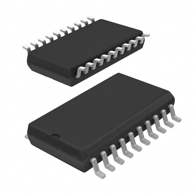
ICGOO电子元器件商城为您提供ADM3251EARWZ由Analog设计生产,在icgoo商城现货销售,并且可以通过原厂、代理商等渠道进行代购。 ADM3251EARWZ价格参考。AnalogADM3251EARWZ封装/规格:数字隔离器, RS232 Digital Isolator 2500Vrms 2 Channel 460Kbps 25kV/µs CMTI 20-SOIC (0.295", 7.50mm Width)。您可以下载ADM3251EARWZ参考资料、Datasheet数据手册功能说明书,资料中有ADM3251EARWZ 详细功能的应用电路图电压和使用方法及教程。
ADM3251EARWZ是Analog Devices Inc.推出的一款集成隔离电源和信号的全双工/半双工数字隔离RS-232收发器,广泛应用于需要电气隔离通信接口的工业与嵌入式系统中。其主要应用场景包括工业自动化控制设备(如PLC、HMI)、仪器仪表、医疗设备以及通信基础设施等。

该器件集成了DC-DC转换器和三通道iCoupler®数字隔离技术,可实现高达2.5kV的隔离耐压,有效防止接地环路干扰、噪声耦合及高压冲击对系统造成损害,提升系统的安全性和可靠性。因其无需外接隔离电源,简化了设计并节省了PCB空间,特别适用于空间受限且要求高抗扰能力的场合。

此外,ADM3251EARWZ支持±15kV ESD保护,适应恶劣工作环境,常用于需长距离串行通信的RS-232接口隔离,例如工控机与传感器、执行器之间的数据传输,或在医疗设备中实现患者连接部分与主控电路之间的安全隔离。总之,它是一款高性能、高集成度的隔离解决方案,适用于对安全性、稳定性和紧凑设计有较高要求的工业与医疗应用。
| 参数 | 数值 |
| 产品目录 | |
| 描述 | DGTL ISO 2.5KV 2CH RS232 20SOIC数字隔离器 Iso SGL CH Line Dvr/Rcvr |
| 产品分类 | |
| 品牌 | Analog Devices Inc |
| 产品手册 | |
| 产品图片 |
|
| rohs | 符合RoHS无铅 / 符合限制有害物质指令(RoHS)规范要求 |
| 产品系列 | 接口 IC,数字隔离器,Analog Devices ADM3251EARWZIsoPower®, iCoupler® |
| 数据手册 | |
| 产品型号 | ADM3251EARWZ |
| PCN设计/规格 | |
| 上升/下降时间(典型值) | 2.3ns, 2.3ns |
| 产品培训模块 | http://www.digikey.cn/PTM/IndividualPTM.page?site=cn&lang=zhs&ptm=19143http://www.digikey.cn/PTM/IndividualPTM.page?site=cn&lang=zhs&ptm=25559 |
| 产品种类 | |
| 传播延迟tpLH/tpHL(最大值) | - |
| 供应商器件封装 | 20-SOIC |
| 共模瞬态抗扰度(最小值) | 25kV/µs |
| 关闭 | No Shutdown |
| 包装 | 管件 |
| 协议 | RS232 |
| 双工 | 全 |
| 商标 | Analog Devices |
| 安装类型 | 表面贴装 |
| 安装风格 | SMD/SMT |
| 封装 | Tube |
| 封装/外壳 | 20-SOIC(0.295",7.50mm 宽) |
| 封装/箱体 | SOIC-20 |
| 工作温度 | -40°C ~ 85°C |
| 工厂包装数量 | 37 |
| 技术 | 磁耦合 |
| 接收器滞后 | 100mV |
| 数据速率 | 460Kbps |
| 最大工作温度 | + 85 C |
| 最大数据速率 | 460 kb/s |
| 最小工作温度 | - 40 C |
| 标准包装 | 37 |
| 电压-电源 | 3.3V,5V |
| 电压-隔离 | 2500Vrms |
| 电源电压-最大 | 5.5 V |
| 电源电压-最小 | 4.5 V |
| 电源电流 | 110 mA |
| 类型 | RS232 |
| 系列 | ADM3251E |
| 绝缘电压 | 2.5 kVrms |
| 脉宽失真(最大) | - |
| 输入-输入侧1/输入侧2 | 1/1 |
| 通道数 | 2 |
| 通道数量 | 1 Channel |
| 通道类型 | 单向 |
| 配用 | /product-detail/zh/EVAL-ADM3251EEBZ/EVAL-ADM3251EEBZ-ND/1938223/product-detail/zh/EVAL-ADM3251EEB1Z/EVAL-ADM3251EEB1Z-ND/2606893 |
| 隔离式电源 | 是 |
| 驱动器/接收器数 | 1/1 |


- 商务部:美国ITC正式对集成电路等产品启动337调查
- 曝三星4nm工艺存在良率问题 高通将骁龙8 Gen1或转产台积电
- 太阳诱电将投资9.5亿元在常州建新厂生产MLCC 预计2023年完工
- 英特尔发布欧洲新工厂建设计划 深化IDM 2.0 战略
- 台积电先进制程称霸业界 有大客户加持明年业绩稳了
- 达到5530亿美元!SIA预计今年全球半导体销售额将创下新高
- 英特尔拟将自动驾驶子公司Mobileye上市 估值或超500亿美元
- 三星加码芯片和SET,合并消费电子和移动部门,撤换高东真等 CEO
- 三星电子宣布重大人事变动 还合并消费电子和移动部门
- 海关总署:前11个月进口集成电路产品价值2.52万亿元 增长14.8%

PDF Datasheet 数据手册内容提取
Isolated, Single-Channel RS-232 Line Driver/Receiver Data Sheet ADM3251E FEATURES FUNCTIONAL BLOCK DIAGRAM 2.5 kV fully isolated (power and data) RS-232 transceiver C1 C3 C2 C4 0.1µF 0.1µF 0.1µF 0.1µF isoPower integrated, isolated dc-to-dc converter 16V 10V 0.1µF 16V 16V 460 kbps data rate 1 Tx and 1 Rx C1+ C1– V+ VISO C2+ C2– V– Meets EIA/TIA-232E specifications ADM3251E VOLTAGE VOLTAGE ESD protection on R and T pins DOUBLER INVERTER IN OUT ±8 kV: contact discharge VCC ±15 kV: air gap discharge OSC RECT REG 0.1 μF charge pump capacitors 0.1µF High common-mode transient immunity: >25 kV/μs ROUT DECODE ENCODE R RIN* Safety and regulatory approvals UL recognition TIN ENCODE DECODE T TOUT 2500 V rms for 1 minute per UL 1577 VDDEI NC eErNti f6i0ca7t4e7 o-5f -C2o (nVfDorEm 0i8t8y4 Teil 2): 2003-01 *INTERNAL 5kΩ PULGL-NDDOWN RESISTOR ON THE RS-232 INPUT. GNDISO 07388-001 CSA Component Acceptance Notice #5A Figure 1. Operating temperature range: −40°C to +85°C Wide body, 20-lead SOIC package APPLICATIONS High noise data communications Industrial communications General-purpose RS232 data links Industrial/telecommunications diagnostic ports Medical equipment GENERAL DESCRIPTION The ADM3251E1 is a high speed, 2.5 kV fully isolated, single- transformer. Special care must be taken during printed circuit channel RS-232/V.28 transceiver device that operates from a board (PCB) layout to meet emissions standards. Refer to single 5 V power supply. Due to the high ESD protection on the Application Note AN-0971, Control of Radiated Emissions with R and T pins, the device is ideally suited for operation in isoPower Devices, for details on board layout considerations. IN OUT electrically harsh environments or where RS-232 cables are The ADM3251E conforms to the EIA/TIA-232E and ITU-T V. 28 frequently being plugged and unplugged. specifications and operates at data rates up to 460 kbps. The ADM3251E incorporates dual-channel digital isolators Four external 0.1 μF charge pump capacitors are used for the with isoPower™ integrated, isolated power. There is no requirement voltage doubler/inverter, permitting operation from a single to use a separate isolated dc-to-dc converter. Chip-scale trans- 5 V supply. former iCoupler® technology from Analog Devices, Inc., is used The ADM3251E is available in a 20-lead, wide body SOIC package both for the isolation of the logic signals as well as for the inte- and is specified over the −40°C to +85°C temperature range. grated dc-to-dc converter. The result is a total isolation solution. The ADM3251E contains isoPower technology that uses high frequency switching elements to transfer power through the 1 Protected by U.S. Patents 5,952,849; 6,873,065; and 7,075,329. Rev. G Document Feedback Information furnished by Analog Devices is believed to be accurate and reliable. However, no responsibility is assumed by Analog Devices for its use, nor for any infringements of patents or other One Technology Way, P.O. Box 9106, Norwood, MA 02062-9106, U.S.A. rights of third parties that may result from its use. Specifications subject to change without notice. No license is granted by implication or otherwise under any patent or patent rights of Analog Devices. Tel: 781.329.4700 ©2008–2013 Analog Devices, Inc. All rights reserved. Trademarks and registered trademarks are the property of their respective owners. Technical Support www.analog.com
ADM3251E Data Sheet TABLE OF CONTENTS Features .............................................................................................. 1 Theory of Operation ...................................................................... 11 Applications ....................................................................................... 1 Isolation of Power and Data ...................................................... 11 Functional Block Diagram .............................................................. 1 Charge Pump Voltage Converter ............................................. 12 General Description ......................................................................... 1 5.0 V Logic to EIA/TIA-232E Transmitter .............................. 12 Revision History ............................................................................... 2 EIA/TIA-232E to 5 V Logic Receiver ...................................... 12 Specifications ..................................................................................... 3 High Baud Rate ........................................................................... 12 Package Characteristics ............................................................... 5 Thermal Analysis ....................................................................... 12 Regulatory Information ............................................................... 5 Insulation Lifetime ..................................................................... 12 Insulation and Safety-Related Specifications ............................ 5 Applications Information .............................................................. 13 DIN EN 60747-5-2 (VDE 0884 TEIL 2): 2003-01 Insulation PCB Layout ................................................................................. 13 Characteristics .............................................................................. 6 Example PCB for Reduced EMI ............................................... 13 Absolute Maximum Ratings ............................................................ 7 DC Correctness and Magnetic Field Immunity ..................... 13 ESD Caution .................................................................................. 7 Isolated Power Supply Circuit .................................................. 14 Pin Configuration and Function Descriptions ............................. 8 Outline Dimensions ....................................................................... 15 Typical Performance Characteristics ............................................. 9 Ordering Guide .......................................................................... 15 REVISION HISTORY 10/13—Rev. F to Rev. G Changes to Pollution Degree and Input–to-Output Test Voltage Added Patents Information, Note 1 ............................................... 1 Parameters, Table 6............................................................................ 6 Changed Minimum External Tracking (Creepage) Value to Added Applications Information Section and Example PCB for 7.6 mm, Table 5 ................................................................................. 5 Reduced EMI Section; Added Table 9 and Table 10; Changes to Pin 9 Description and Pin 11 Descriptions, Table 8 ...... 8 Renumbered Sequentially ............................................................. 13 Changes to Isolation of Power and Data Section ....................... 11 Changes to PCB Layout Section ................................................... 13 Added Isolated Power Supply Circuit Section, and Figure 22; 6/12—Rev. E to Rev. F Renumbered Sequentially ............................................................. 14 Changes to Endnote 1 in Table 4 .................................................... 5 Added DC Correctness and Magnetic Field Immunity 1/10—Rev. B to Rev. C Section .............................................................................................. 13 Changes to Table 4 ............................................................................. 5 Added Figure 22 and Figure 23; Renumbered Sequentially ..... 14 11/09—Rev. A to Rev. B Updated Outline Dimensions and Changes to Changes to Figure 1 ........................................................................... 1 Ordering Guide ............................................................................... 15 Changed to Primary Side Supply Input Current, I CC(DISABLE) Maximum Limit to 2.5 mA .............................................................. 4 5/10—Rev. D to Rev. E Changes to Table 4 ............................................................................. 5 Changes to Features Section............................................................ 1 Changes to Figure 13 ...................................................................... 11 Changes to Table 4 ............................................................................ 5 9/08—Rev. 0 to Rev. A 3/10—Rev. C to Rev. D Changes to Timing Parameters in Table 1 .................................... 3 Changes to Features and General Description Sections .............. 1 Changes to Timing Parameters in Table 2 .................................... 4 Changes to Table 4 and Table 5 ....................................................... 5 Changes to Ordering Guide .......................................................... 14 Changed DIN V VDE V 0884-10 (VDE V 0884-10):2006-12 Insulation Characteristics (Pending) Heading to DIN EN 7/08—Revision 0: Initial Version 60747-5-2 (VDE 0884 Teil 2): 2003-01 Insulation Characteristics ................................................................................... 6 Rev. G | Page 2 of 16
Data Sheet ADM3251E SPECIFICATIONS All voltages are relative to their respective ground; all minimum/maximum specifications apply over the entire recommended operating range; T = 25°C and V = 5.0 V (dc-to-dc converter enabled), unless otherwise noted. A CC Table 1. Parameter Min Typ Max Unit Test Conditions/Comments DC CHARACTERISTICS VCC Operating Voltage Range 4.5 5.5 V DC-to-DC Converter Enable Threshold, VCC(ENABLE)1 4.5 V DC-to-DC Converter Disable Threshold, VCC(DISABLE)1 3.7 V DC-to-DC Converter Enabled Input Supply Current, ICC(ENABLE) 110 mA VCC = 5.5 V, no load 145 mA VCC = 5.5 V, RL = 3 kΩ VISO Output2 5.0 V IISO = 0 µA LOGIC Transmitter Input, TIN Logic Input Current, ITIN −10 +0.01 +10 μA Logic Low Input Threshold, VTINL 0.3 VCC V Logic High Input Threshold, VTINH 0.7 VCC V Receiver Output, ROUT Logic High Output, VROUTH VCC − 0.1 VCC V IROUTH = −20 μA VCC − 0.5 VCC − 0.3 V IROUTH = −4 mA Logic Low Output, VROUTL 0.0 0.1 V IROUTH = 20 μA 0.3 0.4 V IROUTH = 4 mA RS-232 Receiver, RIN EIA-232 Input Voltage Range3 −30 +30 V EIA-232 Input Threshold Low 0.6 2.0 V EIA-232 Input Threshold High 2.1 2.4 V EIA-232 Input Hysteresis 0.1 V EIA-232 Input Resistance 3 5 7 kΩ Transmitter, TOUT Output Voltage Swing (RS-232) ±5 ±5.7 V RL = 3 kΩ to GND Transmitter Output Resistance 300 Ω VISO = 0 V Output Short-Circuit Current (RS-232) ±12 mA TIMING CHARACTERISTICS Maximum Data Rate 460 kbps RL = 3 kΩ to 7 kΩ, CL = 50 pF to 1000 pF Receiver Propagation Delay tPHL 190 ns tPLH 135 ns Transmitter Propagation Delay 650 ns RL = 3 kΩ, CL = 1000 pF Transmitter Skew 80 ns Receiver Skew 70 ns Transition Region Slew Rate3 5.5 10 30 V/μs +3 V to −3 V or −3 V to +3 V, VCC = +3.3 V, RL = 3 kΩ, CL = 1000 pF, TA = 25°C AC SPECIFICATIONS Output Rise/Fall Time, tR/tF (10% to 90%) 2.3 ns CL = 15 pF, CMOS signal levels Common-Mode Transient Immunity at Logic High Output4 25 kV/μs VCM = 1 kV, transient magnitude = 800 V Common-Mode Transient Immunity at Logic Low Output4 25 kV/μs VCM = 1 kV, transient magnitude = 800 V ESD PROTECTION (RIN And TOUT PINS) ±15 kV Human body model air discharge ±8 kV Human body model contact discharge 1 Enable/disable threshold is the VCC voltage at which the internal dc-to-dc converter is enabled/disabled. 2 To maintain data sheet specifications, do not draw current from VISO. 3 Guaranteed by design. 4 VCM is the maximum common-mode voltage slew rate that can be sustained while maintaining specification-compliant operation. VCM is the common-mode potential difference between the logic and bus sides. The transient magnitude is the range over which the common mode is slewed. The common-mode voltage slew rates apply to both rising and falling common-mode voltage edges. Rev. G | Page 3 of 16
ADM3251E Data Sheet All voltages are relative to their respective ground; all minimum/maximum specifications apply over the entire recommended operating range; T = 25°C, V = 3.3 V (dc-to-dc converter disabled), and the secondary side is powered externally by V = 3.3 V, unless A CC ISO otherwise noted. Table 2. Parameter Min Typ Max Unit Test Conditions/Comments DC CHARACTERISTICS VCC Operating Voltage Range 3.0 3.7 V DC-to-DC Converter Disable Threshold, VCC(DISABLE)1 3.7 V DC-to-DC Converter Disabled VISO2 3.0 5.5 V Primary Side Supply Input Current, ICC(DISABLE) 2.5 mA No load Secondary Side Supply Input Current, IISO(DISABLE) 12 mA VISO = 5.5 V, RL = 3 kΩ Secondary Side Supply Input Current, IISO(DISABLE) 6.2 mA RL = 3 kΩ LOGIC Transmitter Input, TIN Logic Input Current, ITIN −10 +0.01 +10 μA Logic Low Input Threshold, VTINL 0.3 VCC V Logic High Input Threshold, VTINH 0.7 VCC V Receiver Output, ROUT Logic High Output, VROUTH VCC − 0.1 VCC V IROUTH = −20 μA VCC − 0.5 VCC − 0.3 V IROUTH = −4 mA Logic Low Output, VROUTL 0.0 0.1 V IROUTH = 20 μA 0.3 0.4 IROUTH = 4 mA RS-232 V Receiver, RIN EIA-232 Input Voltage Range3 −30 +30 V EIA-232 Input Threshold Low 0.6 1.3 V EIA-232 Input Threshold High 1.6 2.4 V EIA-232 Input Hysteresis 0.3 V EIA-232 Input Resistance 3 5 7 kΩ Transmitter, TOUT Output Voltage Swing (RS-232) ±5 ±5.7 V RL = 3 kΩ to GND Transmitter Output Resistance 300 Ω VISO = 0 V Output Short-Circuit Current (RS-232) ±11 mA TIMING CHARACTERISTICS Maximum Data Rate 460 kbps RL = 3 kΩ to 7 kΩ, CL = 50 pF to 1000 pF Receiver Propagation Delay tPHL 190 ns tPLH 135 ns Transmitter Propagation Delay 650 ns RL = 3 kΩ, CL = 1000 pF Transmitter Skew 80 ns Receiver Skew 55 ns Transition Region Slew Rate3 5.5 10 30 V/μs +3 V to −3 V or −3 V to +3 V, VCC = 3.3 V, RL = 3 kΩ, CL = 1000 pF, TA = 25°C AC SPECIFICATIONS Output Rise/Fall Time, tR/tF (10% to 90%) 2.3 ns CL = 15 pF, CMOS signal levels Common-Mode Transient Immunity at Logic High Output4 25 kV/μs VCM = 1 kV, transient magnitude = 800 V Common-Mode Transient Immunity at Logic Low Output4 25 kV/μs VCM = 1 kV, transient magnitude = 800 V ESD PROTECTION (RIN AND TOUT PINS) ±15 kV Human body model air discharge ±8 kV Human body model contact discharge 1 Enable/disable threshold is the VCC voltage at which the internal dc-to-dc converter is enabled/disabled. 2 To maintain data sheet specifications, do not draw current from VISO. 3 Guaranteed by design. 4 VCM is the maximum common-mode voltage slew rate that can be sustained while maintaining specification-compliant operation. VCM is the common-mode potential difference between the logic and bus sides. The transient magnitude is the range over which the common mode is slewed. The common-mode voltage slew rates apply to both rising and falling common-mode voltage edges. Rev. G | Page 4 of 16
Data Sheet ADM3251E PACKAGE CHARACTERISTICS Table 3. Parameter Symbol Min Typ Max Unit Test Conditions Resistance (Input-to-Output) R 1012 Ω I-O Capacitance (Input-to-Output) C 2.2 pF f = 1 MHz I-O Input Capacitance C 4.0 pF I IC Junction-to-Air Thermal Resistance θ 47.05 °C/W JA REGULATORY INFORMATION Table 4. UL1 VDE2 CSA Recognized under 1577 Component Certified according to DIN EN 60747-5-2 (VDE Approved under CSA Component Acceptance Recognition Program 0884 Teil 2):2003-01 Notice #5A File E214100 File 2471900-4880-0001/123328 Basic Insulation per CSA 60950-1-07 and IEC 60950-1, 400 V rms (566 V peak) maximum working voltage File 2268268 1 In accordance with UL 1577, each ADM3251E is proof tested by applying an insulation test voltage ≥3000 V rms for 1 sec (current leakage detection limit = 6 μA). 2 Each ADM3251E is proof tested by applying an insulation test voltage ≥4000 V peak for 1 sec (partial discharge detection limit = 5 pC). INSULATION AND SAFETY-RELATED SPECIFICATIONS Table 5. Parameter Symbol Value Unit Conditions Rated Dielectric Insulation Voltage 2500 V rms 1 minute duration Minimum External Air Gap (Clearance) L(I01) 7.7 mm Measured from input terminals to output terminals, shortest distance through air Minimum External Tracking (Creepage) L(I02) 7.6 mm Measured from input terminals to output terminals, shortest distance path along body Minimum Internal Gap (Internal Clearance) 0.017 mm Distance through insulation Tracking Resistance (Comparative Tracking Index) CTI >175 V DIN IEC 112/VDE 0303 Part 1 Isolation Group IIIa Maximum Working Voltage Compatible with V 425 V peak Continuous peak voltage across the isolation barrier IORM 50-Year Service Life Rev. G | Page 5 of 16
ADM3251E Data Sheet DIN EN 60747-5-2 (VDE 0884 TEIL 2): 2003-01 INSULATION CHARACTERISTICS This isolator is suitable for reinforced isolation only within the safety limit data. Maintenance of the safety data is ensured by protective circuits. Table 6. Description Conditions Symbol Characteristic Unit Installation Classification per DIN VDE 0110 For Rated Mains Voltage ≤ 150 V rms I to IV For Rated Mains Voltage ≤ 300 V rms I to III Climatic Classification 40/105/21 Pollution Degree 2 Maximum Working Insulation Voltage V 424 V peak IORM Input-to-Output Test Voltage Method b1 V × 1.875 = V , 100% production test, t = 1 sec, V 795 V peak IORM PR m PR partial discharge < 5 pC Highest Allowable Overvoltage Transient overvoltage, t = 10 sec V 4000 V peak TR TR Safety-Limiting Values Maximum value allowed in the event of a failure Case Temperature T 150 °C S Supply Current I 531 mA S1 Insulation Resistance at T V = 500 V R >109 Ω S IO S Rev. G | Page 6 of 16
Data Sheet ADM3251E ABSOLUTE MAXIMUM RATINGS Stresses above those listed under Absolute Maximum Ratings Table 7. may cause permanent damage to the device. This is a stress Parameter Rating rating only; functional operation of the device at these or any V , V −0.3 V to +6 V CC ISO other conditions above those indicated in the operational V+ (V − 0.3 V ) to +13 V CC section of this specification is not implied. Exposure to absolute V− –13 V to +0.3 V maximum rating conditions for extended periods may affect Input Voltages device reliability. T −0.3 V to (V + 0.3 V ) IN CC R ±30 V ESD CAUTION IN Output Voltages T ±15 V OUT R −0.3 V to (V + 0.3 V ) OUT CC Short-Circuit Duration T Continuous OUT Power Dissipation θJA, Thermal Impedance 47.05°C/W Operating Temperature Range Industrial −40°C to +85°C Storage Temperature Range −65°C to +150°C Pb-Free Temperature (Soldering, 30 sec) 260°C Rev. G | Page 7 of 16
ADM3251E Data Sheet PIN CONFIGURATION AND FUNCTION DESCRIPTIONS NC 1 20 VISO VCC 2 19 V+ VCC 3 18 C1+ GND 4 ADM3251E 17 C1– GND 5 TOP VIEW 16 TOUT GND 6 (Not to Scale) 15 RIN GND 7 14 C2+ ROUT 8 13 C2– TIN 9 12 V– GND 10NC = NO CONNECT11 GNDISO 07388-002 Figure 2. Pin Configuration Table 8. Pin Function Descriptions Pin No. Mnemonic Description 1 NC No Connect. This pin should always remain unconnected. 2, 3 V Power Supply Input. A 0.1 µF decoupling capacitor is required between V and ground. When a voltage CC CC between 4.5 V and 5.5 V is applied to the V pin, the integrated dc-to-dc converter is enabled. If this voltage CC is lowered to between 3.0 V and 3.7 V, the integrated dc-to-dc converter is disabled. 4, 5, 6, 7, 10 GND Ground. 8 R Receiver Output. This pin outputs CMOS logic levels. OUT 9 T Transmitter (Driver) Input. This pin accepts CMOS levels. IN 11 GND Ground Reference for Isolated RS-232 Side. ISO 12 V− Internally Generated Negative Supply. 13, 14 C2−, C2+ Positive and Negative Connections for Charge Pump Capacitors. External Capacitor C2 is connected between these pins; a 0.1 µF capacitor is recommended, but larger capacitors up to 10 µF can be used. 15 R Receiver Input. This input accepts RS-232 signal levels. IN 16 T Transmitter (Driver) Output. This outputs RS-232 signal levels. OUT 17, 18 C1−, C1+ Positive and Negative Connections for Charge Pump Capacitors. External Capacitor C1 is connected between these pins; a 0.1 µF capacitor is recommended, but larger capacitors up to 10 µF can be used. 19 V+ Internally Generated Positive Supply. 20 V Isolated Supply Voltage for Isolator Secondary Side. A 0.1 µF decoupling capacitor is required between V ISO ISO and ground. When the integrated dc-to-dc converter is enabled, the V pin should not be used to power ISO external circuitry. If the integrated dc-to-dc converter is disabled, power the secondary side by applying a voltage in the range of 3.0 V to 5.5 V to this pin. Rev. G | Page 8 of 16
Data Sheet ADM3251E TYPICAL PERFORMANCE CHARACTERISTICS 12 12 Tx HIGH (VCC = 5V) 10 Tx OUTPUT HIGH (VCC = 5V) 8 8 6 4 Tx HIGH (VISO = 3.3V) 4 Tx OUTPUT HIGH (VISO = 3.3V) V) V) T ( T ( 2 U U P 0 P 0 T T U U O O –2 x x T T –4 Tx LOW (VISO = 3.3V) –4 Tx OUTPUT LOW (VISO = 3.3V) –6 –8 –8 Tx LOW (VCC = 5V) –10 Tx OUTPUT LOW (VCC = 5V) –120 200 LOAD4 0C0APACITAN6C00E (pF) 800 1000 07388-004 –120 1 LOAD CUR2RENT (mA) 3 4 07388-006 Figure 3. Transmitter Output Voltage High/Low vs. Load Figure 6. Transmitter Output Voltage High/Low vs. Load Current Capacitance at 460 kbps 12 15 10 Tx OUTPUT HIGH V+ (VCC = 5V) 10 8 6 V) 4 5 V+ (VISO = 3.3V) Tx OUTPUT ( –220 V+, V– (V) –50 V– (VISO = 3.3V) –4 –6 –10 Tx OUTPUT LOW V– (VCC = 5V) –8 –104.5 4.7 4.9 VCC (V) 5.1 5.3 5.5 07388-005 –150 1 LOAD CUR2RENT (mA) 3 4 07388-007 Figure 4. Transmitter Output Voltage High/Low vs. VCC, RL = 3 kΩ Figure 7. Charge Pump V+, V− vs. Load Current 12 400 V– 10 Tx OUTPUT HIGH 350 8 Ω) 6 CE (300 N UT (V) 42 MPEDA250 V+ TP 0 P I200 U M Tx O–2 E PU150 –4 G R –6 Tx OUTPUT LOW HA100 C –8 50 –10 –123.0 3.5 4.0VISO (V)4.5 5.0 5.5 07388-009 40.50 4.75 VC5C.0 0(V) 5.25 5.5007388-008 Figure 5. Transmitter Output Voltage High/Low vs. VISO, RL = 3 kΩ Figure 8. Charge Pump Impedance vs. VCC Rev. G | Page 9 of 16
ADM3251E Data Sheet 400 350 E (Ω)300 V– IVVD/1 C 5 N DA250 E P M P I200 V+ M V E PU150 D5V/I 2 G R A100 H C 50 VCC=5V 30.00 3.25 3.50 3.75 4.00VI4S.O2 5(V)4.50 4.75 5.00 5.25 5.50 07388-010 LOAD=3kΩAND1nFTIME(500ns/DIV) 07388-012 Figure 9. Charge Pump Impedance vs. VISO Figure 11. 460 kbps Data Transmission 200 5.0 180 4.5 VCC = 5.5V 160 V) 4.0 mA) 140 OLD ( 3.5 SUPPLY CURRENT ( 1120860000 VCC = 4.5V VCC = 5V VOLTAGE THRESHN3221....0505 HLOIGWH TTHHRREESSHHOOLLDD 40 TI1.0 20 0.5 00 46 92 138 DA18T4A R2A3T0E (k2b7p6s) 322 368 414 460 07388-003 40.50 4.75 VC5C.0 (0V) 5.25 5.5007388-011 Figure 10. Primary Supply Current vs. Data Rate Figure 12. TIN Voltage Threshold vs. VCC Rev. G | Page 10 of 16
Data Sheet ADM3251E THEORY OF OPERATION The ADM3251E is a high speed, 2.5 kV fully isolated, single- The T pin accepts CMOS input levels (and TTL levels at IN channel RS-232 transceiver device that operates from a single V = 3.3 V). The driver input signal that is applied to the T CC IN power supply. pin is referenced to logic ground (GND). It is coupled across the isolation barrier, inverted, and then appears at the transceiver The internal circuitry consists of the following main sections: section, referenced to isolated ground (GND ). Similarly, the ISO • Isolation of power and data receiver input (R ) accepts RS-232 signal levels that are IN • A charge pump voltage converter referenced to isolated ground. The R input is inverted and IN • A 5.0 V logic to EIA/TIA-232E transmitter coupled across the isolation barrier to appear at the R pin, OUT • A EIA/TIA-232E to 5.0 V logic receiver referenced to logic ground. C1 C3 C2 C4 The digital signals are transmitted across the isolation barrier 0.1µF 0.1µF 0.1µF 0.1µF 16V 10V 0.1µF 16V 16V using iCoupler technology. Chip-scale transformer windings couple the digital signals magnetically from one side of the barrier to the other. Digital inputs are encoded into waveforms C1+ C1– V+ VISO C2+ C2– V– ADM3251E VOLTAGE VOLTAGE that are capable of exciting the primary transformer of the DOUBLER INVERTER winding. At the secondary winding, the induced waveforms are decoded into the binary value that was originally transmitted. VCC OSC RECT REG There is hysteresis in the V input voltage detect circuit. Once the CC 0.1µF dc-to-dc converter is active, the input voltage must be decreased ROUT DECODE ENCODE R RIN* below the turn-on threshold to disable the converter. This feature ensures that the converter does not go into oscillation due to ENCODE DECODE T TOUT TIN noisy input power. *INTERNAL 5kΩ PULGL-NDDOWN RESISTOR ON THE RS-232 INPUT. GNDISO 07388-013 4.5VTO 5.5V VCC ADM3251E VIVSO+ +C01.031VµF +0.1µF Figure 13. Functional Block Diagram 0.1µF C1+ +C1 0.1µF ISOLATION OF POWER AND DATA C1– 16V The ADM3251E incorporates a dc-to-dc converter section, CMOS OUTPUT ROUT TOUT EIA/TIA-232E OUTPUT which works on principles that are common to most modern RIN EIA/TIA-232E INPUT power supply designs. V power is supplied to an oscillating CMOS INPUT TIN C2+ +C2 CC 0.1µF circuit that switches current into a chip-scale air core transformer. C2– 16V Power is transferred to the secondary side, where it is rectified V– ISOLATION C4 to a high dc voltage. The power is then linearly regulated to BARRIER +0.1µF atob othuet 5V.0IS OV p ainn.d T shuep VplIiSeOd p tion tshheo sueldco nnodta brye usisdeed d taot ap osewcetrio n and GND GNDISO 16V 07388-014 external circuitry. Figure 14. Typical Operating Circuit with the DC-to-DC Converter Enabled (VCC = 4.5 V to 5.5 V) Because the oscillator runs at a constant high frequency 3.0VTO 5.5V ISOLATED SUPPLY independent of the load, excess power is internally dissipated in the output voltage regulation process. Limited space for 3.0VTO 3.7V VISO C3 +0.1µF +0.1µF transformer coils and components also adds to internal power VCC ADM3251E V+ 10V dissipation. This results in low power conversion efficiency. 0.1µF C1+ +C1 0.1µF The ADM3251E can be operated with the dc-to-dc converter C1– 16V enabled or disabled. The internal dc-to-dc converter state of the CMOS OUTPUT ROUT TOUT EIA/TIA-232E OUTPUT ADM3251E is controlled by the input VCC voltage. In normal RIN EIA/TIA-232E INPUT operating mode, VCC is set between 4.5 V and 5.5 V and the CMOS INPUT TIN C2+ +C2 0.1µF internal dc-to-dc converter is enabled. To disable the dc-to-dc C2– 16V converter, lower V to a value between 3.0 V and 3.7 V. In this CC V– mode, the user must externally supply isolated power to the ISOLATION C4 BARRIER +0.1µF VanISdO 5p.i5n V. A ann dis oal asetecdo nsdecaorny dsiadrey isnidpeu tv coultrargeen ot,f IbISeOt,w oef e1n2 3m.0A V GND GNDISO 16V 07388-015 (maximum) is required on the VISO pin. The signal channels of Figure 15. Typical Operating Circuit with the DC-to-DC Converter Disabled the ADM3251E then continue to operate normally. (VCC = 3.0 V to 3.7 V) Rev. G | Page 11 of 16
ADM3251E Data Sheet CHARGE PUMP VOLTAGE CONVERTER THERMAL ANALYSIS The charge pump voltage converter consists of a 200 kHz Each ADM3251E device consists of three internal die, attached oscillator and a switching matrix. The converter generates a to a split-paddle lead frame. For the purposes of thermal analysis, ±10.0 V supply from the input 5.0 V level. This is done in two it is treated as a thermal unit with the highest junction temper- stages by using a switched capacitor technique as illustrated in ature reflected in the θ value from Table 7. The value of θ is JA JA Figure 16 and Figure 17. First, the 5.0 V input supply is doubled based on measurements taken with the part mounted on a to 10.0 V by using C1 as the charge storage element. The +10.0 V JEDEC standard 4-layer PCB with fine-width traces in still air. level is then inverted to generate −10.0 V using C2 as the Following the recommendations in the PCB Layout section storage element. C3 is shown connected between V+ and V , decreases the thermal resistance to the PCB, allowing increased ISO but is equally effective if connected between V+ and GND . thermal margin at high ambient temperatures. ISO Capacitor C3 and Capacitor C4 are used to reduce the output INSULATION LIFETIME ripple. Their values are not critical and can be increased, if All insulation structures eventually break down when subjected desired. Larger capacitors (up to 10 μF) can be used in place of to voltage stress over a sufficiently long period. The rate of C1, C2, C3, and C4. insulation degradation is dependent on the characteristics of the 5.0 V LOGIC TO EIA/TIA-232E TRANSMITTER voltage waveform applied across the insulation. In addition to the testing performed by the regulatory agencies, Analog The transmitter driver converts the 5.0 V logic input levels into Devices carries out an extensive set of evaluations to determine RS-232 output levels. When driving an RS-232 load with V = CC the lifetime of the insulation structure within the ADM3251E. 5.0 V, the output voltage swing is typically ±10 V. S1 S3 The insulation lifetime of the ADM3251E depends on the VISO V+ = 2VISO voltage waveform type imposed across the isolation barrier. The + + C1 C3 S2 S4 iCoupler insulation structure degrades at different rates GND VISO depending on whether the waveform is bipolar ac, unipolar ac, OISNCTIELRLANTAOLR 07388-016 odrif dfecr.e Fnitg iusroela 1t8io, nF ivgoulrtaeg 1e9 w, aanvdef Forigmusr.e 20 illustrate these Figure 16. Charge Pump Voltage Doubler Bipolar ac voltage is the most stringent environment. In the case S1 S3 of unipolar ac or dc voltage, the stress on the insulation is FROM V+ GNDISO VOLTAGE + + significantly lower. DOUBLER S2 C2 S4 C4 GNDISO V– = –(V+) RATED PEAK VOLTAGE OISNCTIELRLANTAOLR 07388-017 0V 07388-019 Figure 18. Bipolar AC Waveform Figure 17. Charge Pump Voltage Inverter RATED PEAK VOLTAGE EIA/TIA-232E TO 5 V LOGIC RECEIVER Tinhpeu rt elceevievle arn ids atrna innsvlaetretsin itg ilnetvoe la- s5h.0if tVer l othgaict aocuctepputts ltehvee lR. TS-h2e3 2 0V 07388-020 Figure 19. Unipolar AC Waveform input has an internal 5 kΩ pull-down resistor to ground and is also protected against overvoltages of up to ±30 V. An uncon- RATED PEAK VOLTAGE nreescitsetodr .i nTphuits ,i st hpeurlelfeodr eto, r 0e sVu lbtsy i tnh ae Linotgeircn 1a lo 5u ktpΩu tp luelvl-edl ofowrn a n 0V 07388-021 unconnected input or for an input connected to GND. The Figure 20. DC Waveform Outline Dimensions receiver has a Schmitt-trigger input with a hysteresis level of 0.1 V. This ensures error-free reception for both a noisy input and for an input with slow transition times. HIGH BAUD RATE The ADM3251E offers high slew rates, permitting data trans- mission at rates well in excess of the EIA/TIA-232E specifications. The RS-232 voltage levels are maintained at data rates up to 460 kbps. Rev. G | Page 12 of 16
Data Sheet ADM3251E APPLICATIONS INFORMATION PCB LAYOUT EXAMPLE PCB FOR REDUCED EMI The ADM3251E requires no external circuitry for its logic The choice of how aggressively EMI must be addressed for a interfaces. Power supply bypassing is required at the input and design to pass emissions levels depends on the requirements of output supply pins (see Figure 21). Bypass capacitors are the design as well as cost and performance trade-offs. conveniently connected between Pin 3 and Pin 4 for V and CC The starting point for this example is a 2-layer PCB. EMI reduc- between Pin 19 and Pin 20 for V . The capacitor value should ISO tions are relative to the emissions and noise from this board. To be between 0.01 μF and 0.1 μF. The total lead length between conform to FCC Class B levels, the emissions at these two both ends of the capacitor and the input power supply pin frequencies must be less than 46 dBμV/m, normalized to 3 m should not exceed 20 mm. antenna distance. As expected, EMI testing confirmed that the Because it is not possible to apply a heat sink to an isolation largest emissions peaks occur at the tank frequency and rectifier device, the device primarily depends on heat dissipating into frequency. the PCB through the ground pins. If the device is used at high A 6-layer PCB that employs edge guarding and buried capacitive ambient temperatures, care should be taken to provide a bypassing, which are EMI mitigation techniques described in thermal path from the ground pins to the PCB ground plane. detail in Application Note AN-0971, was manufactured. The The board layout in Figure 21 shows enlarged pads for Pin 4, stackup of the 6-layer test PCB is shown in Table 9. PCB layout Pin5, Pin 6, Pin 7, Pin 10, and Pin 11. Multiple vias should be Gerber files are available upon request. implemented from each of the pads to the ground plane, which significantly reduce the temperatures inside the chip. The Table 9. PCB Layers dimensions of the expanded pads are left to the discretion of the Layer Description designer and the available board space. Top Components and ground planes VIATO GNDISO Inner Layer 1 VCC planes Inner Layer 2 All tracks 0.1µF NC VISO Inner Layer 3 Blank C3 Inner Layer 4 Buried capacitive plane VCC V+ ADM3251E Bottom Ground planes VCC C1+ 0.1µF C1 EMI testing was repeated on the optimized board. The resulting GND C1– reduction in radiated emissions is shown in Table 10. This GND TOUT board meets FCC Class B standards with no external shielding GND RIN by utilizing buried stitching capacitors and edge fencing. GND C2+ Table 10. EMI Test Results C2 ROUT C2– EMI Test Results 300 MHz 600 MHz 2-Layer PCB Emissions 48 dB 53 dB TIN V– C4 6-Layer PCB Emissions 36 dB 32 dB GND GNDISO Achieved EMI Reduction 12 dB 21 dB NC = NO CONNECT 07388-018 DC CORRECTNESS AND MAGNETIC FIELD IMMUNITY Figure 21. Recommended Printed Circuit Board Layout Positive and negative logic transitions at the isolator input cause In applications involving high common-mode transients, narrow (~1 ns) pulses to be sent to the decoder via the trans- care should be taken to ensure that board coupling across the former. The decoder is bistable and is, therefore, either set or isolation barrier is minimized. Furthermore, the board layout reset by the pulses, indicating input logic transitions. should be designed such that any coupling that does occur equally affects all pins on a given component side. In the absence of logic transitions at the input for more than 1 μs, periodic sets of refresh pulses (indicative of the correct The power supply section of the ADM3251E uses a 300 MHz input state) are sent to ensure dc correctness at the output. If the oscillator frequency to pass power through its chip-scale trans- decoder receives no internal pulses for more than approximately formers. Operation at these high frequencies may raise concerns 5 μs, the input side is assumed to be unpowered or nonfunctional, about radiated emissions and conducted noise. PCB layout and in which case the isolator output is forced to a default state by construction is a very important tool for controlling radiated the watchdog timer circuit. This situation should occur in the emissions. Refer to Application Note AN-0971, Control of ADM3251E during power-up and power-down operations only. Radiated Emissions with isoPower Devices, for extensive guidance on radiation mechanisms and board layout considerations. Rev. G | Page 13 of 16
ADM3251E Data Sheet The limitation on the ADM3251E magnetic field immunity is 1k set by the condition in which induced voltage in the receiving A) DISTANCE = 1m k coil of the transformer is sufficiently large to falsely set or reset T ( 100 N the decoder. The following analysis defines the conditions E R R under which this can occur. U C E 10 The pulses at the transformer output have an amplitude of >1.0 V. ABL DISTANCE = 100mm The decoder has a sensing threshold of about 0.5 V, thus estab- W O lishing a 0.5 V margin in which induced voltages can be tolerated. LL 1 The voltage induced across the receiving coil is given by M A DISTANCE = 5mm U M V = (−dβ/dt)Σπrn2; n = 1, 2, … , N AXI 0.1 M where: βN iiss tthhee mnuamgnbeetric o ffl utuxr dnesn isni ttyh (eg raeucsesi)v.i ng coil. 0.011k 10MkAGNET1IC00 FkIELD FRE1QMUENCY (H1z0)M 100M 07388-201 r is the radius of the nth turn in the receiving coil (cm). n Figure 23. Maximum Allowable Current for Various Current-to-ADM3251E Spacings Given the geometry of the receiving coil internally and an imposed requirement that the induced voltage be, at most, 50% In the presence of strong magnetic fields and high frequencies, of the 0.5 V margin at the decoder, a maximum allowable any loops formed by PCB traces may induce error voltages magnetic field is calculated, as shown in Figure 22. sufficiently large to trigger the thresholds of succeeding 100 circuitry. Exercise care in the layout of such traces to avoid this X possibility. U L C F 10 ISOLATED POWER SUPPLY CIRCUIT TI E N To operate the ADM3251E with its internal dc-to-dc converter AGss) E Mgau 1 disabled, connect a voltage of between 3.0 V and 3.7 V to the ABLY (k VCC pin and apply an isolated power of between 3.0 V and 5.5 V ALLOWDENSIT0.1 Ato ttrhaen VsfoISrOm pienr, drreifveerre nccirecdu tito wGitNhD aI ScOe.n ter-tapped transformer M U and LDO can be used to generate the isolated supply, as shown AXIM 0.01 in Figure 24. The center-tapped transformer provides electrical M isolation of the 5 V power supply. The primary winding of the 0.0011k 10kMAGNETI1C0 0FkIELD FREQ1MUENCY (Hz1)0M 100M 07388-200 t1r8a0n°s foourtm oef rp ihsa esxec witeitdh weaitchh ao pthaeirr .o Af spqauira roef wScahveoftotkrmy ds itohdaet sa aren d Figure 22. Maximum Allowable External Magnetic Flux Density a smoothing capacitor are used to create a rectified signal from the secondary winding. The ADP3330 linear voltage regulator For example, at a magnetic field frequency of 1 MHz, the provides a regulated power supply to the bus side circuitry maximum allowable magnetic field of 0.2 kgauss induces a (V ) of the ADM3251E. ISO voltage of 0.25 V at the receiving coil. This is approximately ISOLATION 50% of the sensing threshold and does not cause a faulty output VCC BARRIER transition. Similarly, if such an event occurs during a transmitted SD103C pulse (and is of the worst-case polarity), the received pulse is 5V IN OUT reduced from >1.0 V to 0.75 V, which is still well above the +22µF SD ADP3330 +10µF 0.5 V sensing threshold of the decoder. TRANSFORMER VCC ERR DRIVER The preceding magnetic flux density values correspond to NR GND specific current magnitudes at given distances from the trans- 78253 SD103C formers. Figure 23 expresses these allowable current magnitudes as a function of frequency for selected distances. As VCC shown in Figure 23, the ADM3251E is extremely immune and can be affected only by extremely large currents operated at VCC VISO high frequency very close to the component. For example, at a ADM3251E magnetic field frequency of 1 MHz, a 0.5 kA current placed 5 mm away from the ADM3251E is required to affect the operation of the component. GND GNDISO 07388-022 Figure 24. Isolated Power Supply Circuit Rev. G | Page 14 of 16
Data Sheet ADM3251E OUTLINE DIMENSIONS 13.00(0.5118) 12.60(0.4961) 20 11 7.60(0.2992) 7.40(0.2913) 1 10 10.65(0.4193) 10.00(0.3937) 0.75(0.0295) 45° 2.65(0.1043) 0.25(0.0098) 0.30(0.0118) 2.35(0.0925) 8° 0.10(0.0039) 0° COPLANARITY 0.10 (01.0.25700) 00..5311((00..00210212)) SPELAATNIENG 00..3230((00..00103709)) 10..2470((00..00510507)) BSC C(RINOEFNPEATRRREOENNLCLTEIHNCEOGOSNDMELISPYM)LAEAIANNRNDSETIAORTRNOOESUJNANEORDDETEEDAICN-POSMPFTRIFALONLMPIDMIRLAELIRATIMTDEEESRTFSMEO;SRIRN-0ECU1QH3SU-EADIVCIINMAELDENENSSTIIOGSNNFS.OR 06-07-2006-A Figure 25. 20-Lead Standard Small Outline Package [SOIC_W] Wide Body (RW-20) Dimensions shown in millimeters and (inches) ORDERING GUIDE Model1 Temperature Range Package Description Package Option ADM3251EARWZ −40°C to +85°C 20-Lead Standard Small Outline Package [SOIC_W] RW-20 ADM3251EARWZ-REEL −40°C to +85°C 20-Lead Standard Small Outline Package [SOIC_W] RW-20 EVAL-ADM3251EEB1Z Evaluation Board 1 Z = RoHS Compliant Part. Rev. G | Page 15 of 16
ADM3251E Data Sheet NOTES ©2008–2013 Analog Devices, Inc. All rights reserved. Trademarks and registered trademarks are the property of their respective owners. D07388-0-10/13(G) Rev. G | Page 16 of 16
Mouser Electronics Authorized Distributor Click to View Pricing, Inventory, Delivery & Lifecycle Information: A nalog Devices Inc.: EVAL-ADM3251EEB1Z ADM3251EARWZ ADM3251EARWZ-REEL