ICGOO在线商城 > 射频/IF 和 RFID > RF 放大器 > ADL5322ACPZ-R7
 Datasheet下载
- 型号: ADL5322ACPZ-R7
- 制造商: Analog
- 库位|库存: xxxx|xxxx
- 要求:
| 数量阶梯 | 香港交货 | 国内含税 |
| +xxxx | $xxxx | ¥xxxx |
查看当月历史价格
查看今年历史价格
ADL5322ACPZ-R7产品简介:
ICGOO电子元器件商城为您提供ADL5322ACPZ-R7由Analog设计生产,在icgoo商城现货销售,并且可以通过原厂、代理商等渠道进行代购。 ADL5322ACPZ-R7价格参考。AnalogADL5322ACPZ-R7封装/规格:RF 放大器, 射频放大器 IC 手机,CDMA2000,W-CDMA,GSM 700MHz ~ 1GHz 8-LFCSP-VD(3x3)。您可以下载ADL5322ACPZ-R7参考资料、Datasheet数据手册功能说明书,资料中有ADL5322ACPZ-R7 详细功能的应用电路图电压和使用方法及教程。
ADL5322ACPZ-R7是Analog Devices Inc.推出的一款高性能RF放大器,广泛应用于无线通信系统中。该器件工作频率范围宽(100 MHz至4000 MHz),具备高增益(典型值为20.5 dB)、低噪声系数(约2.6 dB)和出色的线性度,适合需要高动态性能的射频信号放大场景。

其主要应用场景包括:蜂窝通信基础设施中的基站前端模块、微波点对点通信系统、宽带无线接入设备(如WiMAX)、射频测试仪器以及国防电子系统中的雷达和电子战设备。此外,ADL5322ACPZ-R7也适用于多载波、多标准无线电系统,能够支持GSM、WCDMA、LTE等多种通信标准。

该器件采用紧凑的6引脚SC-70封装,功耗低,输出IP3高(OIP3约+40 dBm),在保持高线性度的同时有效减少信号失真,确保信号传输质量。集成内部匹配和偏置电路,简化了设计流程,降低了外围元件需求,提升了系统可靠性。

综上,ADL5322ACPZ-R7是一款适用于高性能、宽频带射频系统的理想增益模块,特别适合对信号完整性与系统稳定性要求较高的通信和工业应用场合。
| 参数 | 数值 |
| 产品目录 | |
| 描述 | IC AMP GAIN 700-1000MHZ 8-LFCSP |
| 产品分类 | |
| 品牌 | Analog Devices Inc |
| 数据手册 | |
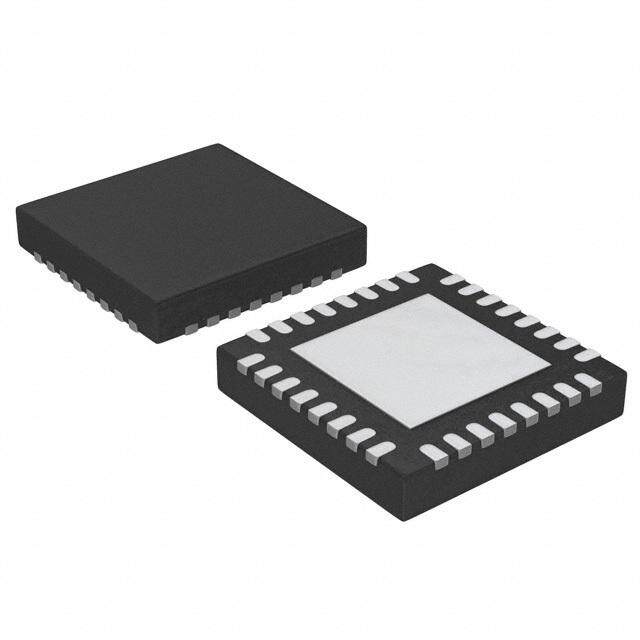
| 产品图片 |
|
| P1dB | 27dBm(501.2mW)~ 27.7dBm(588.8mW) |
| 产品型号 | ADL5322ACPZ-R7 |
| PCN其它 | |
| RF类型 | 手机,CDMA2000,W-CDMA,GSM |
| rohs | 无铅 / 符合限制有害物质指令(RoHS)规范要求 |
| 产品系列 | - |
| 产品培训模块 | http://www.digikey.cn/PTM/IndividualPTM.page?site=cn&lang=zhs&ptm=24737 |
| 产品目录页面 | |
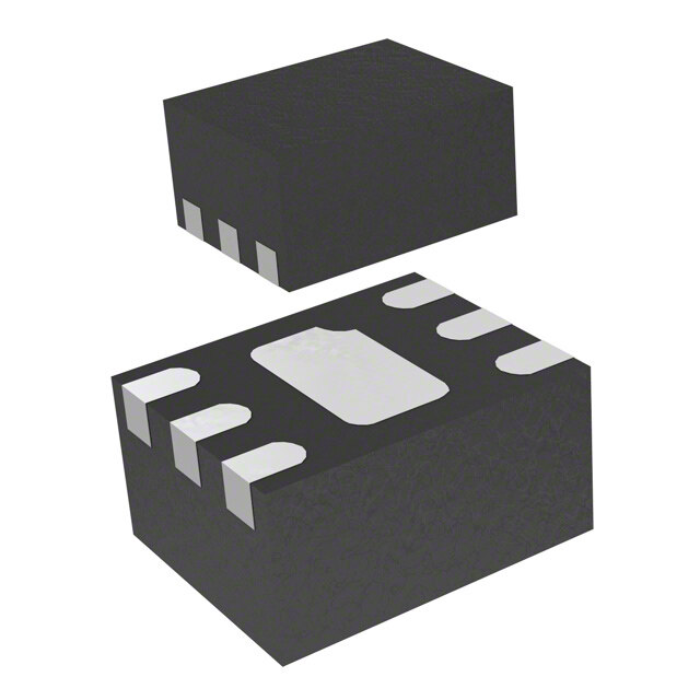
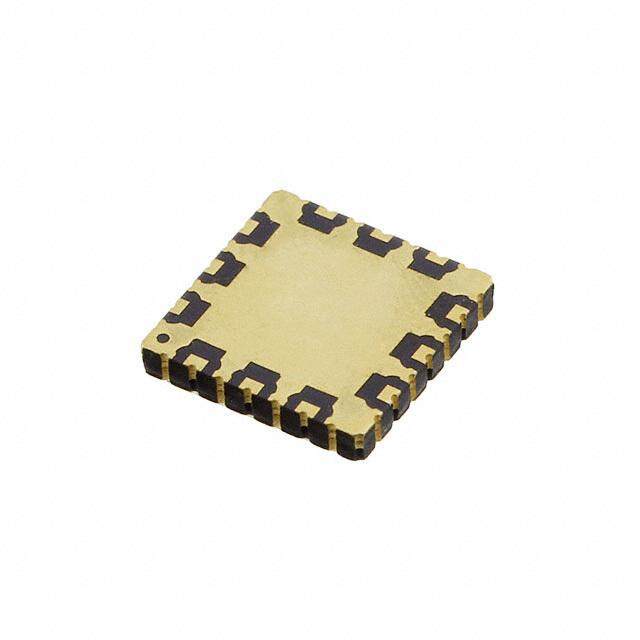
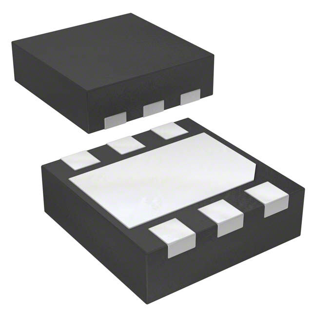
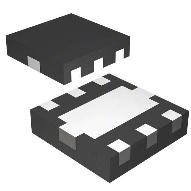
| 供应商器件封装 | 8-LFCSP-VD(3x3) |
| 其它名称 | ADL5322ACPZ-R7CT |
| 包装 | 剪切带 (CT) |
| 噪声系数 | 5dB |
| 增益 | 19dB ~ 21.4dB |
| 封装/外壳 | 8-VFDFN 裸露焊盘,CSP |
| 标准包装 | 1 |
| 测试频率 | 850MHz |
| 电压-电源 | 4.75 V ~ 5.25 V |
| 电流-电源 | 320mA |
| 视频文件 | http://www.digikey.cn/classic/video.aspx?PlayerID=1364138032001&width=640&height=505&videoID=2245193150001 |
| 频率 | 700MHz ~ 1GHz |


- 商务部:美国ITC正式对集成电路等产品启动337调查
- 曝三星4nm工艺存在良率问题 高通将骁龙8 Gen1或转产台积电
- 太阳诱电将投资9.5亿元在常州建新厂生产MLCC 预计2023年完工
- 英特尔发布欧洲新工厂建设计划 深化IDM 2.0 战略
- 台积电先进制程称霸业界 有大客户加持明年业绩稳了
- 达到5530亿美元!SIA预计今年全球半导体销售额将创下新高
- 英特尔拟将自动驾驶子公司Mobileye上市 估值或超500亿美元
- 三星加码芯片和SET,合并消费电子和移动部门,撤换高东真等 CEO
- 三星电子宣布重大人事变动 还合并消费电子和移动部门
- 海关总署:前11个月进口集成电路产品价值2.52万亿元 增长14.8%


PDF Datasheet 数据手册内容提取
700 MHz to 1000 MHz GaAs Matched RF PA Predriver Data Sheet ADL5322 FEATURES FUNCTIONAL BLOCK DIAGRAM Internally matched to 50 Ω input and output Internally biased Operating frequency: 700 MHz to 1000 MHz BIAS CONTROL VCC 5 4 RFOUT Gain: 20 dB OIP3: 45 dBm OUETPUT GND 6 MATCH 3 GND P1 dB: 27 dBm UTCH Noise figure: 5 dB GND 7 INPMAT 2 VCC 3 mm × 3 mm LFCSP RFIN 8 T 1 VCC Power supply: 5 V APPLICATIONS ADL5322 06057-001 CDMA2000, WCDMA, and GSM base station transceivers and E Figure 1. high power amplifiers L GENERAL DESCRIPTION O The ADL5322 is a high linearity GaAs driver amplifier that is internally matched to 50 Ω for operation in the 700 MHz to 1000 MHz frequency range. The amplifier, which has a gain of 20 dB, is specially designed for use in the output stagSe of a cellular base station radio or as an input preamplifier in a multicarrier base station power amplifier. Matching and biasing are all on-chip. The ADL5322 is available in a Pb-free, 3 mm × 3 mm, 8-lead LFCSP package with an opBerating temperature from −40°C to +85°C. O Rev. A Document Feedback Information furnished by Analog Devices is believed to be accurate and reliable. However, no responsibility is assumed by Analog Devices for its use, nor for any infringements of patents or other One Technology Way, P.O. Box 9106, Norwood, MA 02062-9106, U.S.A. rights of third parties that may result from its use. Specifications subject to change without notice. No license is granted by implication or otherwise under any patent or patent rights of Analog Devices. Tel: 781.329.4700 ©2006–2014 Analog Devices, Inc. All rights reserved. Trademarks and registered trademarks are the property of their respective owners. Technical Support www.analog.com
ADL5322 Data Sheet TABLE OF CONTENTS Features .............................................................................................. 1 Pin Configuration and Function Descriptions ..............................5 Applications ....................................................................................... 1 Typical Performance Characteristics ..............................................6 Functional Block Diagram .............................................................. 1 Basic Connections .............................................................................8 General Description ......................................................................... 1 CDMA2000 Driving Application ................................................8 Revision History ............................................................................... 2 Evaluation Board ............................................................................ 10 Specifications ..................................................................................... 3 Outline Dimensions ....................................................................... 11 Absolute Maximum Ratings ............................................................ 4 Ordering Guide .....................................E..................................... 11 ESD Caution .................................................................................. 4 T REVISION HISTORY 1/14—Rev. 0 to Rev. A: Changes to Figure 2 .......................................................................... 5 E Added Figure 12, Renumbered Sequentially ................................ 7 Added Exposed Pad Notation to Outline Dimensions ............. 11 Changes to Ordering Guide .......................................................... 11 L 7/06—Revision 0: Initial Version O S B O Rev. A | Page 2 of 12
Data Sheet ADL5322 SPECIFICATIONS V = 5 V, T = 25°C. CC A Table 1. Parameter Test Conditions/Comments Min Typ Max Unit FREQUENCY RANGE 700 1000 MHz GAIN Frequency = 850 MHz 19 20.3 21.4 dB vs. Frequency 832 MHz to 870 MHz ±0.125 dB vs. Temperature −40°C to +85°C ±1 dB vs. Voltage 5 V, @ 5% (4.75 V to 5.25 V) E±0.1 dB Frequency = 900 MHz 18.6 19.9 21.1 dB vs. Frequency 869 MHz to 894 MHz ±0.125 dB vs. Temperature −40°C to +85°C ±1 dB T vs. Voltage 5 V, @ 5% (4.75 V to 5.25 V) ±0.1 dB Frequency = 950 MHz 18.3 19.6 20.8 dB vs. Frequency 925 MHz to 960 MHz ±0.125 dB vs. Temperature −40°C to +85°C E ±1.1 dB vs. Voltage 5 V, @ 5% (4.75 V to 5.25 V) ±0.1 dB P1 dB Frequency = 850 MHz 27.0 27.7 dBm vs. Frequency 832 MHz to 870 MHz ±0.1 dBm L vs. Temperature −40°C to +85°C ±1 dBm vs. Voltage 5 V, @ 5% (4.75 V to 5.25 V) ±0.3 dBm Frequency = 900 MHz 27.3 27.9 dBm O vs. Frequency 869 MHz to 894 MHz ±0.1 dBm vs. Temperature −40°C to +85°C ±1 dBm vs. Voltage 5 V, @ 5% (4.75 V to 5.25 V) ±0.4 dBm Frequency = 950 MHz 26.7 27.5 dBm S vs. Frequency 925 MHz to 960 MHz ±0.2 dBm vs. Temperature −40°C to +85°C ±1 dBm vs. Voltage 5 V, @ 5% (4.75 V to 5.25 V) ±0.4 dBm NOISE FIGURE FreqBuency = 830 MHz to 960 MHz 5 dB INPUT RETURN LOSS Frequency = 830 MHz to 960 MHz −10 dB OUTPUT RETURN LOSS Frequency = 830 MHz to 960 MHz −10 dB OIP3 Carrier spacing = 1 MHz, P = 5 dBm per carrier O OUT Frequency = 850 MHz 44.8 dBm vs. Frequency 832 MHz to 870 MHz ±0.25 dBm vs. Temperature −40°C to +85°C ±3.0 dBm vs. Voltage 5 V, @ 5% (4.75 V to 5.25 V) ±0.5 dBm Frequency = 900 MHz 45.3 dBm vs. Frequency 869 MHz to 894 MHz ±0.25 dBm vs. Temperature −40°C to +85°C ±2.7 dBm vs. Voltage 5 V, @ 5% (4.75 V to 5.25 V) ±0.8 dBm Frequency = 950 MHz 44.4 dBm vs. Frequency 925 MHz to 960 MHz ±0.25 dBm vs. Temperature −40°C to +85°C ±2.2 dBm vs. Voltage 5 V, @ 5% (4.75 V to 5.25 V) ±0.8 dBm POWER SUPPLY Supply Voltage 4.75 5 5.25 V Supply Current P = 5 dBm 320 mA OUT Operating Temperature −40 +85 °C Rev. A | Page 3 of 12
ADL5322 Data Sheet ABSOLUTE MAXIMUM RATINGS Table 2. Stresses above those listed under Absolute Maximum Ratings Parameter Rating may cause permanent damage to the device. This is a stress Supply Voltage, VPOS 6 V rating only; functional operation of the device at these or any Input Power (re: 50 Ω) 18 dBm other conditions above those indicated in the operational Equivalent Voltage 1.8 V rms section of this specification is not implied. Exposure to absolute θ (Soldered) 28.5°C/W maximum rating conditions for extended periods may affect JC Maximum Junction Temperature 150°C device reliability. Operating Temperature Range −40°C to +85°C ESD CAUTION E Storage Temperature Range −65°C to +150°C Soldering Temperature 260°C T E L O S B O Rev. A | Page 4 of 12
Data Sheet ADL5322 PIN CONFIGURATION AND FUNCTION DESCRIPTIONS VCC 1 8 RFIN VCC 2 ADL5322 7 GND GND 3 TOP VIEW 6 GND (Not to Scale) RFOUT 4 5 VCC N1 . O CVTOIAEN SAN LEOCWT T IMHEP EEDXAPNOCSEEDPAPDADDLDEL.ETO THE GROUND PLANE 06057-002 Figure 2. Pin Configuration E Table 3. Pin Function Descriptions Pin No. Mnemonic Description 1, 2, 5 VCC Positive 5 V Supply Voltage. Bypass these three pins with independent power supply decoupling T networks (100 pF, 10 nF, and 10 µF). 3, 6, 7 GND Device Ground. 4 RFOUT RF Output. Internally matched to 50 Ω. 8 RFIN RF Input. Internally matched to 50 Ω. E N/A EP Exposed Paddle. Connect to the ground plane via a low impedance path. L Table 4. S-Parameters Frequency ADL5322 (1, 1) ADL5322 (1, 2) ADL5322 (2, 1) ADL5322 (2, 2) 700.0 MHz 0.210/109.457 0.002/97.018 +11.221/−158.622 0.436/150.470 O 720.0 MHz 0.195/104.437 0.002/93.284 +11.108/−166.579 0.392/145.211 740.0 MHz 0.179/99.101 0.002/87.856 +11.013/−174.596 0.345/137.443 760.0 MHz 0.165/93.363 0.002/86.137 10.931/177.282 0.295/133.051 780.0 MHz 0.151/86.953 0.002/78.668 10.856/169.006 0.242/125.612 800.0 MHz 0.138/79.928 0S.002/74.072 10.781/160.613 0.187/116.434 820.0 MHz 0.125/71.950 0.002/68.940 10.698/152.065 0.130/102.897 840.0 MHz 0.114/62.829 0.002/62.269 10.605/143.342 0.079/76.154 860.0 MHz 0.103/52.162 0.002/56.742 10.493/134.489 0.061/18.090 B 880.0 MHz 0.095/39.531 0.002/56.696 10.361/125.433 +0.098/−26.962 900.0 MHz 0.090/24.952 0.003/43.549 10.210/116.239 +0.153/−46.741 920.0 MHz 0.088/9.188 0.003/37.254 10.033/106.889 +0.211/−58.300 940.0 MHz +0.090O/−7.350 0.003/29.904 9.837/97.326 +0.269/−66.606 960.0 MHz +0.095/−23.642 0.003/24.334 9.614/87.600 +0.324/−73.265 980.0 MHz +0.104/−39.131 0.003/16.521 9.364/77.609 +0.376/−78.914 1.000 GHz +0.115/−53.477 0.003/8.139 9.081/67.342 +0.424/−83.911 Rev. A | Page 5 of 12
ADL5322 Data Sheet TYPICAL PERFORMANCE CHARACTERISTICS 22.0 5.6 21.5 5.4 TEMP = –40°C 21.0 5.2 20.5 TEMP = +25°C 5.0 dB)20.0 B) AIN (19.5 NF (d 4.8 E G TEMP = +85°C 4.6 19.0 4.4 18.5 T 18.0 4.2 17.5 4.0 800 850 FREQUE9N0C0Y (MHz) 950 1000 06057-003 700 E800FREQUENCY (MHz9)00 1000 06057-006 Figure 3. Gain vs. Frequency, V = 5 V, T = −40°C, +25°C, and +85°C Figure 6. Noise Figure vs. Frequency, Multiple Devices, V = 5 V, T = 25°C CC A S A 29.0 2L8.4 TEMP = –40°C 28.2 28.5 28.0 VCC = 5.25V O 27.8 VCC = 5V 28.0 m) TEMP = +25°C m)27.6 VCC = 4.75V B B B (d27.5 B (d27.4 P1d S P1d27.2 27.0 27.0 TEMP = +85°C 26.8 26.5 B 26.6 26.0800 850 FREQUE9N0C0Y (MHz) 950 1000 06057-004 26.4800 850 FREQUE9N0C0Y (MHz) 950 1000 06057-007 Figure 4. P1 dB vs. Frequency, V = 5 V, T = −40°C, +25°C, and +85°C Figure 7. P1 dB vs. Frequency, V = 4.75 V, 5 V, and 5.25 V, T = 25°C CC OA CC A 47 46.5 TEMP = –40°C 46 46.0 VCC = 5.25V 45.5 45 Bm) TEMP = +25°C Bm)45.0 OIP3 (d 44 OIP3 (d44.5 VCC = 5V 43 44.0 VCC = 4.75V 42 43.5 TEMP = +85°C 41800 850 FREQUE9N0C0Y (MHz) 950 1000 06057-005 43.0800 850 FREQUE9N0C0Y (MHz) 950 1000 06057-008 Figure 5. OIP3 vs. Frequency, V = 5 V, T = −40°C, +25°C, and +85°C Figure 8. OIP3 vs. Frequency, V = 4. 75 V, 5 V, and 5.25 V, T = 25°C CC A CC A Rev. A | Page 6 of 12
Data Sheet ADL5322 6 7 6 5 5 4 Y Y NC NC 4 E E U 3 U Q Q RE RE 3 F F 2 2 E 1 1 0 0 44.1 44.3 44.5 44.7OI4P43. 9(dBm45).1 45.3 45.5 45.7 06057-009 43.6 43.8 44.0T44.2OI4P43. 4(dBm44).6 44.8 45.0 45.2 06057-011 Figure 9. Distribution of OIP3 at 850 MHz Figure 11. Distribution of OIP3 at 950 MHz –6 650 E –8 600 –10 TA = –40°C 2 [1, 1] (dB)2 [2, 2] (dB) –––111462 S22 LURRENT (mA) 455505000 TTAA ==++2855CC L532L532 –18 S11 O LY C 400 DD P AA P 350 –20 U S –22 300 –24 S 250 –260.70 0.75 0.8F0REQUE0N.8C5Y (GHz0).90 0.95 1.00 06057-010 2002 4 6 8 10 12 P14OUT1 6(dB1m8) 20 22 24 26 28 30 06057-112 Figure 10. Input S11 and Output S22 RetuBrn Loss vs. Frequency Figure 12. Supply Current vs. P and Temperature V = 5 V, T = −40°C, OUT CC A +25°C, and +85°C O Rev. A | Page 7 of 12
ADL5322 Data Sheet BASIC CONNECTIONS Figure 15 shows the basic connections for operating the CDMA2000 DRIVING APPLICATION ADL5322. Each of the three power supply lines should be Figure 14 shows a plot of the spectrum of an ADL5323 driving decoupled with 10 µF, 10 nF, and 100 pF capacitors. Pin 3, Pin 6, at 4-carrier CDMA2000 signal at 0 dBm per carrier (total Pin 7, and the exposed paddle under the device should all be carrier power = 6 dBm), centered at 880 MHz. At 750 kHz connected to a low impedance ground plane. If multiple ground and 1.98 MHz offset, adjacent channel power ratios of −59 dBc planes are being used, these should be stitched together with and −84 dBc (measured in 30 kHz with respect to the 1.22 MHz vias under the device to optimize thermal conduction. See carrier) are observed. At 4 MHz carrier offset, −73 dBc is recommended land pattern in Figure 13. measured in a 1 MHz bandwidth (−133 dBm/Hz). Note that E the spectrum of the four carriers is slightly rounded due the frequency response of the cavity-tuned filter that was used to filter out the noise and distortion of the source signal. –10 T RBW = 30kHz VBW = 300kHz –20 SWT = 2s RF ATT = 20dB –30 MIXER = –10dBm –40 E CH PWR = 0.26dBm ACP UP = –59.33dB ALT1 UP = –84.35dB –50 ALT2 UP = –72.74dB m) B –60 d ( L –70 06057-013 –80 Figure 13. Recommended Land Pattern –90 O –100 –110CENTER 881.875MHz 1MHz/ SPAN 10MHz 06057-014 Figure 14. Spectrum of 4 Adjacent CDMA2000 Carriers Centered at 880 MHz; S Total Carrier Power = 6 dBm (0 dBm per Carrier) B C5 100pF RFOUT VCC C1 C3 C2 10µF O10nF 100pF AGND AGND AGND ADL5322 5 VCC RFOUT 4 AGND 6 GND GND 3 7 GND VCC 2 VCC 8 RFIN VCC 1 C6 C7 C8 AGND EP 100pF 10nF 10µF C4 AGND AGND AGND 100pF VCC RFIN C9 C10 C11 A10G0NpDF A10GnNFD 1A0GµNFD 06057-012 Figure 15. Basic Connections Rev. A | Page 8 of 12
Data Sheet ADL5322 Figure 16 shows how ACP varies with output power level. The –30 –30 close-in ACP is a function of the signal coding and is unaffected by output headroom at these power levels. The ACP measured Bc) –40 –40 d at 1.98 MHz carrier offset is −72 dBc at 10 dBm output power W ( –50 –50 m) B B (12 dB below the required 60 dBc). At 4 MHz carrier offset, the Hz R ACP1 (dBc) – 750kHz OFFSET – 30kHz RBW W (d natprretooa q6iwnsu esdei mrrBae nomidtdft b e−(dryt3i,o s t1ttthhoa deirls)Bt C iocomDoun rt (Mmpr1eu AesMtap 2spoHu0on0rzwde0)dse, s rwtit noa(h 0 naai cd nd1ha B aM rimndsH t.1 ep8zne nbdr aaBcn-a rdbrewrefieleiordrwrt)eh. dw Ii nsoh −uaat7 t5 p5i0su d tdB Bmm P1 AND ACP2 – 30k –––678000 ACP3 (dBm) – 4MHz OFFSET – 1MHz RBW –––678000 ACP3 – 1MHz RB AC –90 ACP2 (dBc) – 1.98MHz OFFSET –E 30kHz RBW –90 –100 –100 –10 –8 –6 –4OUTT–P2UT PO0WER 2(dBm)4 6 8 10 06057-015 Figure 16. CDMA2000 ACP vs. Output Power per Carrier; 4 Adjacent Carriers E L O S B O Rev. A | Page 9 of 12
ADL5322 Data Sheet EVALUATION BOARD Figure 18 shows the schematic of the ADL5322 evaluation board. The board is powered by a single supply in the 4.75 V to 5.25 V range. The power supply is decoupled on each of the three power supply pins by 10 µF, 10 nF, and 100 pF capacitors. See Table 5 for exact evaluation board component values. Note that all three VCC pins (Pin 1, Pin 2, and Pin 5) should be independently bypassed as shown in Figure 18 for proper operation. E 06057-016 Figure 17. Evaluation Board Component Side View T Table 5. Evaluation Board Components Component Function Default Value E DUT1 Driver amplifier ADL5322 C1, C12, C16 Low frequency bypass capacitors 10 µF, 0603 C3, C11, C17 Low frequency bypass capacitors 10 nF, 0402 C2, C10, C18 High frequency bypass capacitors L 100 pF, 0402 C8, C9, C13, C14, R3 Open Open, 0402 R2, R4 AC coupling capacitors 100 pF, 0402 O R4 100pF RFOUT C13 C14 VCC OPEN OPEN C1 C3 C2 S AGND AGND 10µF 10nF 100pF AGND AGND AGND ADL5322/ ADL5323 B 5 VCC RFOUT 4 AGND TP2 6 GND GND 3 7 GND VCC 2 VCC 8 RFIN VCC 1 C10 C11 C12 AGND 100pF 10nF 10µF R2 DUT1 AGND AGND AGND O100pF RFIN RO3PEN TP1 C8 C9 OPEN OPEN SNS1 VCC AGND AGND C18 C17 C16 100pF 10nF 10µF GND VCC VCC AGND AGND AGND AGND W1 VCC AGND 06057-017 Figure 18. Evaluation Board Schematic Rev. A | Page 10 of 12
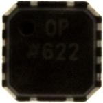
Data Sheet ADL5322 OUTLINE DIMENSIONS 3.25 3.00 SQ 0.60 MAX 0.50 2.75 BSC 0.60 MAX 5 8 2.95 1.60 INDICAPTINO R1 VTIOEPW 22..7555 SQ (EBOXTPPTOAOMDS VIEEWD) 11..4350 4 1 PIN 1 00..5400 1.89 INDICATOR E 12° MAX 0.70 MAX 0.30 1.74 0.90 MAX 0.65TYP 1.59 0.85 NOM 0.05 MAX FOR PROPER CONNECTION OF 0.01 NOM THE EXPOSED PAD, REFER TO SEPALTAINNGE 000...321038 0.20 REF TFSHUEENC CTPITIONION CN OO DFNE FTSIHGCISUR RIDPAATTTIOIAON NSS HAENTEDT. 04-04-2012-A Figure 19. 8-Lead Lead Frame Chip Scale Package [LFCSP_VD] 3 mm × 3 mm Body, Very Thin, Dual Lead E (CP-8-2) Dimensions shown in millimeters ORDERING GUIDE L Model1 Temperature Range Package Description Package Option Branding Ordering Quantity ADL5322ACPZ-R7 −40°C to +85°C 8-Lead LFCSP_VD, 7" Tape and Reel CP-8-2 OP 1500 ADL5322ACPZ-WP −40°C to +85°C 8-Lead LFCSP_VD, Waffle Pack CP-8-2 OP 50 O ADL5322-EVALZ Evaluation Board 1 1 Z = RoHS Compliant Part. S B O Rev. A | Page 11 of 12
ADL5322 Data Sheet NOTES E T E L O S B O ©2006–2014 Analog Devices, Inc. All rights reserved. Trademarks and registered trademarks are the property of their respective owners. D06057-0-1/14(A) Rev. A | Page 12 of 12