ICGOO在线商城 > 传感器,变送器 > 运动传感器 - IMU(惯性测量装置) > ADIS16210CMLZ
 Datasheet下载
- 型号: ADIS16210CMLZ
- 制造商: Analog
- 库位|库存: xxxx|xxxx
- 要求:
| 数量阶梯 | 香港交货 | 国内含税 |
| +xxxx | $xxxx | ¥xxxx |
查看当月历史价格
查看今年历史价格
ADIS16210CMLZ产品简介:
ICGOO电子元器件商城为您提供ADIS16210CMLZ由Analog设计生产,在icgoo商城现货销售,并且可以通过原厂、代理商等渠道进行代购。 ADIS16210CMLZ价格参考。AnalogADIS16210CMLZ封装/规格:运动传感器 - IMU(惯性测量装置), Accelerometer, Inclinometer, 3 Axis Sensor SPI Output。您可以下载ADIS16210CMLZ参考资料、Datasheet数据手册功能说明书,资料中有ADIS16210CMLZ 详细功能的应用电路图电压和使用方法及教程。
ADIS16210CMLZ是由Analog Devices Inc.(ADI公司)生产的一款运动传感器,属于惯性测量装置(IMU)系列。它是一款高性能、低成本的MEMS陀螺仪模块,专为需要精确角度测量和旋转检测的应用而设计。以下是其主要应用场景:

 1. 工业设备
   - 机器人控制:用于工业机器人中,提供精确的姿态和角速度信息,帮助实现平稳的运动控制。
   - 平台稳定系统:在无人机、云台或摄影设备中,用于检测和补偿振动或倾斜,确保设备的稳定性。
   - 机械臂校准:在多关节机械臂中,用于实时监测各关节的角度变化,提高操作精度。

 2. 航空航天与国防
   - 导航系统:作为惯性导航的一部分,用于测量飞行器或车辆的旋转角度和姿态。
   - 导弹制导:提供高精度的角速率数据,支持导弹的稳定性和方向控制。
   - 飞行器姿态控制:在小型无人机或无人驾驶飞行器中,用于检测和调整飞行姿态。

 3. 交通运输
   - 车辆动态控制:在汽车电子稳定程序(ESP)中,用于检测车辆的侧倾和转向角度,提升行车安全性。
   - 列车监控:监测列车运行中的振动和倾斜情况,确保行驶平稳性。
   - 船舶导航:为船舶提供稳定的航向和姿态信息,防止因波浪导致的过度摇摆。

 4. 医疗设备
   - 康复训练:在康复设备中,用于监测患者的身体姿势和运动轨迹,辅助康复治疗。
   - 步态分析:通过测量人体的旋转角度和运动状态,帮助医生评估患者的行走能力。

 5. 消费电子
   - 游戏控制器:为虚拟现实(VR)或增强现实(AR)设备提供精确的头部或手部运动跟踪。
   - 智能家居:用于智能安防设备,检测门窗的开启角度或物体的移动状态。

 6. 其他应用
   - 地震监测:在地震预警系统中,用于检测地面的微小振动和倾斜变化。
   - 管道检测:在管道爬行机器人中,用于实时监测设备的姿态和方向。

ADIS16210CMLZ以其高集成度、低功耗和高可靠性,适用于各种需要精确角度测量和动态监测的场景。
| 参数 | 数值 |
| 产品目录 | |
| 描述 | IC INCLINOMETER/ACCELERMTR MSM加速计 Prec Triaxial w/ SPI |
| 产品分类 | |
| 品牌 | Analog Devices Inc |
| 产品手册 | |
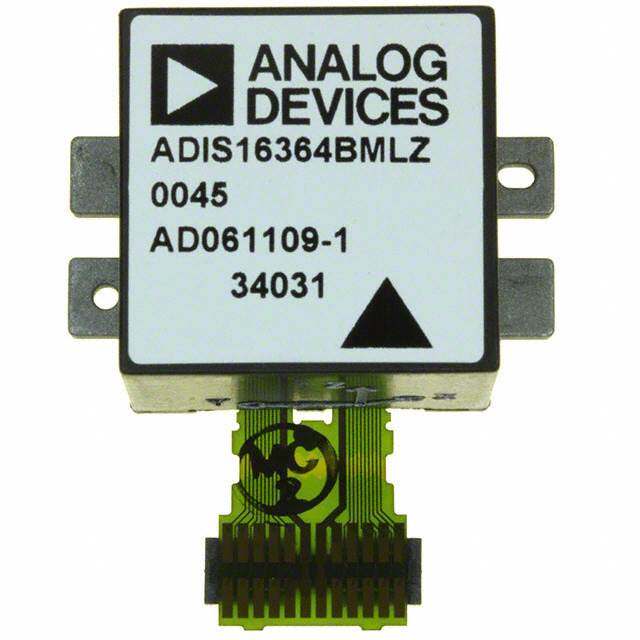
| 产品图片 |
|
| rohs | RoHS 合规性豁免含铅 / 不受限制有害物质指令(RoHS)规范要求限制 |
| 产品系列 | 加速计,Analog Devices ADIS16210CMLZ- |
| 数据手册 | |
| 产品型号 | ADIS16210CMLZ |
| 产品种类 | 加速计 |
| 传感器类型 | 倾角计和加速计 |
| 传感轴 | Triple |
| 分辨率 | 16 bit |
| 加速 | 1.7 g |
| 商标 | Analog Devices |
| 封装 | Bulk |
| 封装/箱体 | Aluminum Package with Flex Connector |
| 工厂包装数量 | 10 |
| 接口 | SPI |
| 数字输出-位数 | 16 bit |
| 数字输出-总线接口 | SPI |
| 最大工作温度 | + 85 C |
| 最小工作温度 | - 40 C |
| 标准包装 | 1 |
| 电源电压-最大 | 3.6 V |
| 电源电压-最小 | 3.15 V |
| 电源电流 | 18 uA |
| 系列 | ADIS16210 |
| 输出类型 | 数字 - SPI |


- 商务部:美国ITC正式对集成电路等产品启动337调查
- 曝三星4nm工艺存在良率问题 高通将骁龙8 Gen1或转产台积电
- 太阳诱电将投资9.5亿元在常州建新厂生产MLCC 预计2023年完工
- 英特尔发布欧洲新工厂建设计划 深化IDM 2.0 战略
- 台积电先进制程称霸业界 有大客户加持明年业绩稳了
- 达到5530亿美元!SIA预计今年全球半导体销售额将创下新高
- 英特尔拟将自动驾驶子公司Mobileye上市 估值或超500亿美元
- 三星加码芯片和SET,合并消费电子和移动部门,撤换高东真等 CEO
- 三星电子宣布重大人事变动 还合并消费电子和移动部门
- 海关总署:前11个月进口集成电路产品价值2.52万亿元 增长14.8%


PDF Datasheet 数据手册内容提取
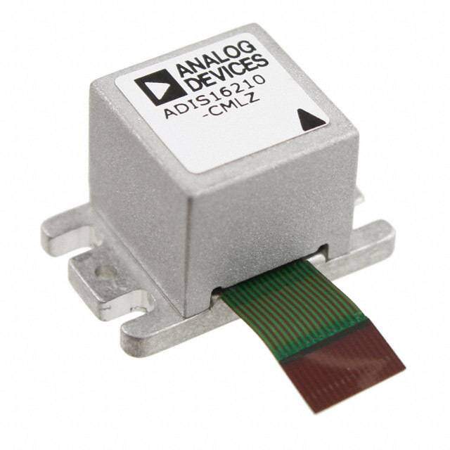
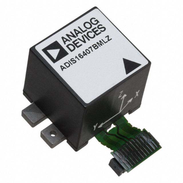
Precision Triaxial Inclinometer and Accelerometer with SPI Data Sheet ADIS16210 FEATURES GENERAL DESCRIPTION Triaxial, digital inclinometer system The ADIS16210 iSensor® is a digital inclinometer system that ±180° measurement range, roll and pitch axes provides precise measurements for both pitch and roll angles ±90° gravity axis over a full orientation range of ±180°. It combines a MEMS tri- ±0.1° relative accuracy axial acceleration sensor with signal processing, addressable user Triaxial, digital accelerometer, high accuracy registers for data collection/programming, and a SPI-compatible ±1.7 g measurement range serial interface. In addition, the production process includes unit ±0.05° axis-to-axis alignment specific calibration for optimal accuracy performance. It also Digital internal temperature measurements offers digital temperature sensor and power supply measurements Digital internal power supply measurements together with configuration controls for in-system calibration, Programmable user calibration options sample rate, filtering, alarms, input/output (I/O) configuration, Single command, frame alignment and power management. Manual accelerometer bias correction The MEMS sensor elements are bound to an aluminum core for Programmable operation and control tight platform coupling and excellent mechanical stability. An Sample rate/filtering internal clock drives the data sampling system, which eliminates Alarm conditions and indicator output the need for an external clock source. The SPI and data buffer Input/output: data ready, alarm, general-purpose structure provide convenient access to accurate sensor data and Power management functions configuration controls. SPI-compatible serial interface Serial number and device ID The ADIS16210 is available in a 15 mm × 24 mm × 15 mm Single-supply operation: 3.0 V to 3.6 V module that provides mounting tabs with M2-sized mounting Calibrated temperature range: −40°C to +85°C holes and a flexible, edge terminated connector interface. It has 15 mm × 24 mm × 15 mm package with flexible connector an extended operating temperature range of −40°C to +125°C. APPLICATIONS Platform control, stabilization, and alignment Tilt sensing, inclinometers, and leveling Motion/position measurement Monitor/alarm devices (security, medical, safety) Navigation FUNCTIONAL BLOCK DIAGRAM DIO1 DIO2 RST VDD ADIS16210 SELF TEST I/O ALARMS MANPAOGWEEMRENT GND TRIAXIAL MEMS SENSOR CONTROLLER CONTROL CS REGISTERS TEMPERATURE SPI SCLK SENSOR PORT SUPPLY DFIIGLTITEARL CAOLRIGRANENMCDTEINOTN CALINIBCRLAINTEION REOGUITSPTUETRS DDIONUT 09593-001 Figure 1. Rev. D Document Feedback Information furnished by Analog Devices is believed to be accurate and reliable. However, no responsibility is assumed by Analog Devices for its use, nor for any infringements of patents or other One Technology Way, P.O. Box 9106, Norwood, MA 02062-9106, U.S.A. rights of third parties that may result from its use. Specifications subject to change without notice. No license is granted by implication or otherwise under any patent or patent rights of Analog Devices. Tel: 781.329.4700 ©2011–2018 Analog Devices, Inc. All rights reserved. Trademarks and registered trademarks are the property of their respective owners. Technical Support www.analog.com
ADIS16210 Data Sheet TABLE OF CONTENTS Features .............................................................................................. 1 System Tools .................................................................................... 15 Applications ....................................................................................... 1 Global Commands ..................................................................... 15 General Description ......................................................................... 1 Input/Output Functions ............................................................ 15 Functional Block Diagram .............................................................. 1 Device Identification .................................................................. 16 Revision History ............................................................................... 2 Status/Error Flags ....................................................................... 16 Specifications ..................................................................................... 3 Flash Memory Management ..................................................... 16 Timing Specifications .................................................................. 4 Alarms .............................................................................................. 17 Absolute Maximum Ratings ............................................................ 5 System Alarm .............................................................................. 17 ESD Caution .................................................................................. 5 Static Alarms ............................................................................... 17 Pin Configuration and Function Descriptions ............................. 6 Dynamic Alarms ........................................................................ 17 Basic Operation ................................................................................. 7 Alarm Reporting ........................................................................ 17 Reading Sensor Data .................................................................... 7 Applications Information .............................................................. 18 Device Configuration .................................................................. 7 Mating Connector ...................................................................... 18 User Register Map ............................................................................ 8 Breakout Board ........................................................................... 18 Sensor Data ........................................................................................ 9 PC-Based Evaluation Tools ....................................................... 18 Output Data Registers .................................................................. 9 Outline Dimensions ....................................................................... 20 Signal Processing, Bias Correction, and Alignment .................. 12 Ordering Guide .......................................................................... 20 REVISION HISTORY 3/2018—Rev C to Rev. D Changes to Signal Processing, Bias Correction, and Alignment Changes to Figure 4 .......................................................................... 6 Section, Figure 16, and Accelerometer Bias Correction Section .. 12 Deleted Interface Board Section, Figure 23, and Figure 25; Added Table 27, Table 28, and Table 29; Renumbered Renumbered Sequentially .............................................................. 18 Sequentially ..................................................................................... 12 Added Breakout Board Section, PC-Based Evaluation Tools Changes to Table 30 and Measurement Mode Section ............. 13 Section, and Figure 24; Renumbered Sequentially .................... 18 Added Two-Axis Mode Section.................................................... 13 Added Figure 25 .............................................................................. 19 Added User Reference Alignment Section, Table 31, Table 32, Changes to Ordering Guide .......................................................... 20 and Table 33 .................................................................................... 14 Change to Table 34 ......................................................................... 15 12/2016—Rev. B to Rev. C Moved User Register Save to Flash Memory Section and Changes to Signal Processing, Bias Correction, and Alignment Figure 20 .......................................................................................... 15 Section .............................................................................................. 12 Changes to Figure 25 ...................................................................... 18 6/2015—Rev. A to Rev. B 6/2011—Rev. 0 to Rev. A Changes to Figure 2 .......................................................................... 4 Changes to Table 1 ............................................................................. 3 Change to Figure 5 ........................................................................... 7 Changes to Table 23 ....................................................................... 12 Changes to User Register Map Section and Table 8 ..................... 8 Changes to Figure 24 and Figure 25............................................. 17 4/2011—Revision 0: Initial Version Rev. D | Page 2 of 20
Data Sheet ADIS16210 SPECIFICATIONS T = −40°C to +85°C, VDD = 3.0 V to 3.6 V, unless otherwise noted. A Table 1. Parameter Test Conditions/Comments Min Typ Max Unit INCLINOMETERS Measurement Range −180 +180 Degrees Relative Accuracy ±30°, AVG_CNT ≥ 0x0009, µ ± 3 σ ±0.1 Degrees ±60°, AVG_CNT ≥ 0x0009, µ ± 1 σ ±0.1 Degrees ±60°, AVG_CNT ≥ 0x0009, µ ± 3 σ ±0.15 Degrees ±180°, AVG_CNT ≥ 0x0009, µ ± 1 σ ±0.14 Degrees ±180°, AVG_CNT ≥ 0x0009, µ ± 3 σ ±0.21 Degrees Noise Density T = 25°C, AVG_CNT = 0x0000 ±0.011 °/√Hz A ACCELEROMETERS Measurement Range ±1.7 g Offset Error µ ± 1 σ ±1 mg Sensitivity Error µ ± 1 σ ±0.0244 % Nonlinearity ±1 g, µ ± 1 σ ±1 ±2 mg Misalignment Axis to axis, deviation from 90°, µ ± 1 σ ±0.05 Degrees Noise Density T = 25°C, AVG_CNT = 0x0000 190 µg/√Hz A Bandwidth −3 dB decrease in dc sensitivity, T = 25°C 50 Hz A Sensor Resonant Frequency T = 25°C 5.5 kHz A LOGIC INPUTS1 Input High Voltage, V 2.0 V INH Input Low Voltage, V 0.8 V INL Logic 1 Input Current, I V = 3.3 V ±0.2 ±1 µA INH IH Logic 0 Input Current, I V = 0 V INL IL All Except RST −40 −60 µA RST −1 mA Input Capacitance, C 10 pF IN DIGITAL OUTPUTS1 Output High Voltage, V I = 1.6 mA 2.4 V OH SOURCE Output Low Voltage, V I = 1.6 mA 0.4 V OL SINK FLASH MEMORY Endurance2 10,000 Cycles Data Retention3 T = 85°C 20 Years J START-UP TIME4 Initial Startup 156 ms Reset Recovery5 RST pulse low or Register GLOB_CMD[7] = 1 33.8 ms Sleep Mode Recovery After CS assertion from high to low 22.3 ms CONVERSION RATE Register AVG_CNT = 0x0000 512 SPS Clock Accuracy 3 % POWER SUPPLY Operating voltage range, VDD 3.0 3.3 3.6 V Power Supply Current Normal mode, T = 25°C 18 mA A Sleep mode, T = 25°C 230 µA A 1 The digital I/O signals are 5 V tolerant. 2 Endurance is qualified as per JEDEC Standard 22, Method A117, and measured at −40°C, +25°C, +85°C, and +125°C. 3 Retention lifetime equivalent at junction temperature (TJ) = 85°C as per JEDEC Standard 22, Method A117. Retention lifetime decreases with junction temperature. See Figure 22. 4 The start-up times presented do not include the data capture time, which is dependent on the AVG_CNT register settings. 5 The RST pin must be held low for at least 15 ns. Rev. D | Page 3 of 20
ADIS16210 Data Sheet TIMING SPECIFICATIONS T = 25°C, VDD = 3.3 V, unless otherwise noted. A Table 2. Parameter Description Min1 Typ Max Unit f SCLK frequency 10 830 kHz SCLK t Stall period between data, between 16th and 17th SCLK 40 μs STALL t Chip select to SCLK edge 48.8 ns CS t DOUT valid after SCLK edge 100 ns DAV t DIN setup time before SCLK rising edge 24.4 ns DSU t DIN hold time after SCLK rising edge 48.8 ns DHD t SCLK rise time 12.5 ns SR t SCLK fall time 12.5 ns SF t , t DOUT rise/fall times 5 12.5 ns DF DR t CS high after SCLK edge 5 ns SFS 1 Guaranteed by design, not tested. Timing Diagrams tSR tDF,tDR CS t SF t t CS SFS 1 2 3 4 5 6 15 16 SCLK t DAV DOUT MSB DB14 DB13 DB12 DB11 DB10 DB2 DB1 LSB t t DSU DHD DIN R/W A6 A5 A4 A3 A2 D2 D1 LSB 09593-002 Figure 2. SPI Timing and Sequence t STALL CS SCLK 09593-003 Figure 3. DIN Bit Sequence Rev. D | Page 4 of 20
Data Sheet ADIS16210 ABSOLUTE MAXIMUM RATINGS Table 3. Table 4. Package Characteristics Parameter Rating Package Type θ θ Device Weight JA JC Acceleration 15-Lead Module 31°C/W 11°C/W 7.2 grams Any Axis, Unpowered 3500 g Any Axis, Powered 3500 g ESD CAUTION VDD to GND −0.3 V to +6.0 V Digital Input Voltage to GND −0.3 V to +5.3 V Digital Output Voltage to GND −0.3 V to VDD + 0.3 V Analog Inputs to GND −0.3 V to +3.6 V Operating Temperature Range −40°C to +125°C Storage Temperature Range −65°C to +150°C Stresses at or above those listed under Absolute Maximum Ratings may cause permanent damage to the product. This is a stress rating only; functional operation of the product at these or any other conditions above those indicated in the operational section of this specification is not implied. Operation beyond the maximum operating conditions for extended periods may affect product reliability. Rev. D | Page 5 of 20
ADIS16210 Data Sheet PIN CONFIGURATION AND FUNCTION DESCRIPTIONS PIN 1 PIN 15 PIN 15 PIN 1 TOP VIEW BOTTOM VIEW NOTES 1. THE LEADS ARE LOCATED ON THE BOTTOM SIDE OF THE FLEXIBLE CABLE. 2. THE LEAD FINISH IS IMMERSION GOLD OVER THE ELECTROLESS NICKEL. 3. THE THICKNESS OF THE GOLD FINISH IS BETWEEN 0.035µm AND 0.150µm. 4. PACKAGE IS NOT SUITABLE FOR SOLDER REFLOW ASSEMBLY PROCESSES. 5. EXAMPLE MATING CONNECTOR: FPAL/VNAX:T 0C 4FO-L6RE2PX8O8IB-R0L1AE5T -CI0O0ON0N-8N4E6C.TOR (FFC) 09593-004 Figure 4. Pin Configuration Table 5. Pin Function Descriptions Pin No. Mnemonic Type1 Description 1, 2 VDD S Power Supply, 3.3 V. 3, 4, 5, 8 GND S Ground. 6, 9 DNC I Do Not Connect. Do not connect to these pins. 7 DIO2 I/O Digital Input/Output Line 2. 10 RST I Reset, Active Low. 11 DIN I SPI, Data Input. 12 DOUT O SPI, Data Output. DOUT is an output when CS is low. When CS is high, DOUT is in a three-state, high impedance mode. 13 SCLK I SPI, Serial Clock. 14 CS I SPI, Chip Select. 15 DIO1 I/O Digital Input/Output Line 1. 1 S is supply, I is input, O is output, and I/O is input/output. Rev. D | Page 6 of 20
Data Sheet ADIS16210 BASIC OPERATION The ADIS16210 is an autonomous system that requires no user READING SENSOR DATA initialization. Upon receiving a valid power supply, it initializes A single register read requires two 16-bit SPI cycles. The first itself and starts sampling, processing, and loading data into the cycle requests the contents of a register using the bit assignments output registers. When using the factory default configuration, in Figure 9. The register contents then follow on DOUT, during DIO1 provides a data ready signal. The SPI interface enables the second sequence. simple integration with many embedded processor platforms, Figure 6 includes three single register reads in succession. In this as shown in Figure 5 (electrical connection) and Table 6 (processor example, the process starts with DIN = 0x0400 to request the pin descriptions). contents of the XACCL_OUT register, followed by 0x0600 to 3.3V request the contents of the YACCL_OUT register, and then 0x0800 VDD to request the contents of the ZACCL_OUT register. Full duplex 1 2 operation enables processors to use the same 16-bit SPI cycle to SYSTEM PROCESSOR SS 14 CS ADIS16210 read data from DOUT while requesting the next set of data SPI MASTER SCLK 13 SCLK on DIN. MOSI 11 DIN DIN 0x0400 0x0600 0x0800 MISO 12 DOUT IRQ 15 DIO31 4 5 8 DOUT XACCL_OUT YACCL_OUT ZACCL_OUT 09593-007 09593-006 Figure 7 providesF aignu erex 6a.m SPpI lRee oadf fEoxaumr pSlPe IR esimgonvael s when reading Figure 5. Electrical Connection Diagram PROD_ID in a repeating pattern. Table 6. Generic Master Processor Pin Names and Functions CS Pin Name Function SS Slave select SCLK IRQ Interrupt request, optional DIN DIN = 0101 0110 0000 0000 = 0x5600 MOSI Master output, slave input MSCISLOK MSearsiatel cr lioncpku t, slave output DOUT DFOiUgTu r=e 070.1 S1P 1I1 R1e1a 0d1 0E1x 1a1m00p =le 0, xS3eFc5o2n =d 1 1662-1B0it Sequence 09593-008 The ADIS16210 SPI interface supports full duplex serial commu- DEVICE CONFIGURATION nication (simultaneous transmit and receive) and uses the bit The user register map (see Table 8) provides a variety of control sequence shown in Figure 9. Table 7 provides a list of the most registers, which enable optimization for specific applications. common settings that initialize the serial port of a processor for the The SPI provides access to these registers, one byte at a time, ADIS16210 SPI interface. using the bit assignments shown in Figure 9. Each register has Table 7. Generic Master Processor SPI Settings 16 bits, where Bits[7:0] represent the lower address and Bits[15:8] Processor Setting Description represent the upper address. Figure 8 displays the SPI signal Master ADIS16210 operates as a slave pattern for writing 0x07 to Address 0x38, which sets the number SCLK Rate ≤ 830 kHz Maximum serial clock rate of averages to 128 and the sample rate to 4 SPS. SPI Mode 3 CPOL = 1 (polarity), CPHA = 1 (phase) CS MSB-First Mode Bit sequence 16-Bit Mode Shift register/data length SCLK DINDIN = 1011 1000 0000 0111 = 0xB807, SET AVG_CNT[7:0] = 0x07 09593-009 Figure 8. Example SPI Write Pattern CS SCLK DIN R/W A6 A5 A4 A3 A2 A1 A0 DC7 DC6 DC5 DC4 DC3 DC2 DC1 DC0 R/W A6 A5 DOUT D15 D14 D13 D12 D11 D10 D9 D8 D7 D6 D5 D4 D3 D2 D1 D0 D15 D14 D13 NOTES 12..FWDOOHRUE TNO BTCHISTE SIRS A DHREIEGV HPIC,R EDOSOD.UUTC EISD I NO NAL TYH WREHEE-NS TTAHTEE P, RHEIGVHIO IUMSP E16D-ABNITC DEI NM OSEDQE,U WENHCICEH S ATLALROTWS SW MITUHL RT/IWFU =N C0.TIONAL USE OF THE LINE 09593-113 Figure 9. SPI Communication Bit Sequence Rev. D | Page 7 of 20
ADIS16210 Data Sheet USER REGISTER MAP Table 8. User Register Memory Map1 Name R/W Flash Backup Address Size (Bytes) Function Reference FLASH_CNT R Yes 0x00 2 Diagnostics, flash write counter (16-bit binary) Table 43 SUPPLY_OUT R No 0x02 2 Output, power supply Table 20 XACCL_OUT R No 0x04 2 Output, x-axis acceleration Table 9 YACCL_OUT R No 0x06 2 Output, y-axis acceleration Table 10 ZACCL_OUT R No 0x08 2 Output, z-axis acceleration Table 11 TEMP_OUT R No 0x0A 2 Output, internal temperature Table 18 XINCL_OUT R No 0x0C 2 Output, ±180° x-axis inclination Table 13 YINCL_OUT R No 0x0E 2 Output, ±180° y-axis inclination Table 14 ZINCL_OUT R No 0x10 2 Output, ±180° z-axis inclination Table 15 XACCL_NULL R/W Yes 0x12 2 Calibration, x-axis acceleration offset null Table 24 YACCL_NULL R/W Yes 0x14 2 Calibration, y-axis acceleration offset null Table 25 ZACCL_NULL R/W Yes 0x16 2 Calibration, z-axis acceleration offset null Table 26 X_ALIGN_REF R Yes 0x18 2 Calibration, x-axis alignment reference Table 31 Y_ALIGN_REF R Yes 0x1A 2 Calibration, y-axis alignment reference Table 32 Z_ALIGN_REF R Yes 0x1C 2 Calibration, z-axis alignment reference Table 33 Reserved N/A N/A 0x1E 2 Reserved, do not write to these locations N/A ALM_MAG_X R/W Yes 0x20 2 Alarm, x-axis amplitude threshold Table 45 ALM_MAG_Y R/W Yes 0x22 2 Alarm, y-axis amplitude threshold Table 46 ALM_MAG_Z R/W Yes 0x24 2 Alarm, z-axis amplitude threshold Table 47 ALM_MAG_S R/W Yes 0x26 2 Alarm, system alarm threshold Table 48 ALM_SMPL_X R/W Yes 0x28 2 Alarm, x-axis sample period Table 49 ALM_SMPL_Y R/W Yes 0x2A 2 Alarm, y-axis sample period Table 50 ALM_SMPL_Z R/W Yes 0x2C 2 Alarm, z-axis sample period Table 51 ALM_CTRL R/W Yes 0x2E 2 Operation, alarm control Table 44 Reserved N/A N/A 0x30 2 Reserved N/A GPIO_CTRL R/W Yes 0x32 2 Operation, general I/O configuration and data Table 37 MSC_CTRL R/W Yes 0x34 2 Operation, orientation mode Table 30 DIO_CTRL R/W Yes 0x36 2 Operation, digital I/O configuration and data Table 36 AVG_CNT R/W Yes 0x38 2 Operation, decimation filter configuration Table 22 SLP_CNT R/W Yes 0x3A 2 Operation, sleep count Table 35 DIAG_STAT R No 0x3C 2 Diagnostics, system status register Table 42 GLOB_CMD W No 0x3E 2 Operation, system command register Table 34 Reserved N/A N/A 0x40 to 0x51 16 Reserved N/A LOT_ID1 R N/A 0x52 2 Lot identification, Code 1 Table 38 LOT_ID2 R N/A 0x54 2 Lot identification, Code 2 Table 39 PROD_ID R N/A 0x56 2 Production identification number Table 40 SERIAL_NUM R N/A 0x58 2 Serial number Table 41 Reserved N/A N/A 0x5A to 0x06F 22 Reserved N/A XACCL_BIAS R/W Yes 0x70 2 Calibration, x-axis accelerometer internal bias Table 27 YACCL_BIAS R/W Yes 0x72 2 Calibration, y-axis accelerometer internal bias Table 28 ZACCL_BIAS R/W Yes 0x74 2 Calibration, z-axis accelerometer internal bias Table 29 1 N/A means not applicable. Rev. D | Page 8 of 20
Data Sheet ADIS16210 SENSOR DATA OUTPUT DATA REGISTERS Inclinometers The ADIS16210 provides a set of output registers for three The XINCL_OUT (see Table 13), YINCL_OUT (see Table 14), orthogonal axes of acceleration: incline angles, internal and ZINCL_OUT (see Table 15) registers provide access to temperature, and power supply. incline angle data for each axis. For example, set DIN = 0x0E00 to request y-axis data (YINCL_OUT). Use the following process Accelerometers to translate the contents of these registers into degrees (°): The accelerometers respond to both static (gravity) and dynamic 1. Convert the 16-bit, twos complement number into a acceleration using the polarity shown in Figure 10. XACCL_OUT decimal equivalent. (see Table 9), YACCL_OUT (see Table 10), and ZACCL_OUT (see 2. Multiply the decimal equivalent by 180. Table 11) provide user access to digital calibrated accelerometer 3. Divide the result of Step 2 by 32,768. data for each axis. For example, use DIN = 0x0400 to request the x-axis data (XACCL_OUT). After reading the contents of one Table 16 provides several examples of this data format. of these registers, convert the 16-bit, twos complement number Table 13. XINCL_OUT (Base Address = 0x0C), Read Only into a decimal equivalent, and then divide that number by 16,384 Bits Description to convert the measurement into units of gravity (g). Table 12 [15:0] X-axis inclinometer output data, binary, provides several examples of this data format. 0° = 0x0000, 1 LSB = 180°/32,768 = ~0.0055°/LSB Table 9. XACCL_OUT (Base Address = 0x04), Read Only Table 14. YINCL_OUT (Base Address = 0x0E), Read Only Bits Description Bits Description [15:0] X-axis accelerometer output data, twos complement, 1 LSB = 1 g ÷ 16,384 = ~61 µg/LSB, 0 g = 0x0000 [15:0] Y-axis inclinometer output data, binary, 0° = 0x0000, 1 LSB = 180°/32,768 = ~0.055°/LSB Table 10. YACCL_OUT (Base Address = 0x06), Read Only Bits Description Table 15. ZINCL_OUT (Base Address = 0x10), Read Only [15:0] Y-axis accelerometer output data, twos complement, Bits Description 1 LSB = 1 g ÷ 16,384 = ~61 µg/LSB, 0 g = 0x0000 [15:0] Z-axis inclinometer output data, binary, 0° = 0x0000, 1 LSB = 180°/32,768 = ~0.0055°/LSB Table 11. ZACCL_OUT (Base Address = 0x08), Read Only Bits Description Table 16. Incline Angle Data Format Examples [15:0] Z-axis accelerometer output data, twos complement, Orientation Decimal Hex Binary 1 LSB = 1 g ÷ 16,384 = ~61 µg/LSB, 0 g = 0x0000 +179.9945° +32,767 0x7FFF 0111 1111 1111 1111 +0.011° +2 0x0002 0000 0000 0000 0010 Table 12. Accelerometer Data Format Examples +0.0055° +1 0x0001 0000 0000 0000 0001 Orientation (g) Decimal Hex Binary 0° 0 0x0000 0000 0000 0000 0000 +1.7 +27,853 0x6CCD 0110 1100 1100 1101 −0.0055° −1 0xFFFF 1111 1111 1111 1111 +1 +16,384 0x4000 0100 0000 0000 0000 −0.011° −2 0xFFFE 1111 1111 1111 1110 +2/16,384 +2 0x0002 0000 0000 0000 0010 −180° −32,768 0x8000 1000 0000 0000 0000 +1/16,384 +1 0x0001 0000 0000 0000 0001 0 0 0x0000 0000 0000 0000 0000 Figure 10 through Figure 15 provide orientation examples and −1/16,384 −1 0xFFFF 1111 1111 1111 1111 the associated output values for each accelerometer and incli- −2/16,384 −2 0xFFFE 1111 1111 1111 1110 nometer register. These examples assume the factory default −1 −16,384 0xC000 1100 0000 0000 0000 configuration for the gravity vector (z-axis, pointed up). See the −1.7 −27,853 0x9333 1001 0011 0011 0011 MSC_CTRL (see Table 30) for additional options for gravity vector definitions. Rev. D | Page 9 of 20
ADIS16210 Data Sheet a X a aY aX Z aY aZ 09593-012 09593-014 Figure 10. Inclinometer Output Example, 0° Tilt Figure 13. Inclinometer Output Example, +30° Y-Axis Tilt a X a a Y a Z X a Z a Y 09593-013 09593-017 Figure 11. Inclinometer Output Example, −30° Y-Axis Tilt Figure 14. Inclinometer Output Example, +30° X-Axis Tilt a Z a Y a X a X a Y a Z 09593-016 09593-015 Figure 12. Inclinometer Output Example, −30° X-Axis Tilt Figure 15. Inclinometer Output Example, 180° Tilt Table 17. Orientation/Output Examples for Z-Axis Gravity Orientation1 Register Figure 10 Figure 11 Figure 12 Figure 13 Figure 14 Figure 15 XACCL_OUT 0 0 −8192 0 +8192 0 YACCL_OUT 0 −8192 0 +8192 0 0 ZACCL_OUT +16,384 +14,189 +14,189 +14,189 +14,189 −16,384 XINCL_OUT 0 0 −5462 0 +5462 −32,768 YINCL_OUT 0 −5462 0 +5462 0 −32,768 ZINCL_OUT +16,384 +10,922 +10,922 +10,922 +10,922 −16,384 1 Register setting for Z-axis gravity orientation is MSC_CTRL[7:0] = xxxx xx10. Rev. D | Page 10 of 20
Data Sheet ADIS16210 Internal Temperature Power Supply The TEMP_OUT register (see Table 18) provides access to an The SUPPLY_OUT register (see Table 20) provides a digital internal temperature measurement. Set DIN = 0x0A00 to request measurement for the supply voltage on the VDD pins (see the contents of this register. Use the following process to translate Table 5). Set DIN = 0x0200 to request the contents of this the contents of TEMP_OUT into degrees Celsius (°C): register. Use the following process to translate the contents of SUPPLY_OUT into volts (V): 1. Convert the 12-bit binary number into a decimal equivalent. 1. Convert the 16-bit binary number into a decimal 2. Subtract 1278 from the decimal equivalent. equivalent. 3. Multiply the result of Step 2 by −0.47. 2. Multiply the decimal equivalent by 5. 4. Add 25 to the result of Step 3. 3. Divide the result of Step 2 by 32,768. Table 19 provides several examples of this data format. Note that Table 21 provides several examples of this data format. this internal temperature measurement provides an indicator of Table 20. SUPPLY_OUT (Base Address = 0x02), Read Only condition changes, not an absolute measurement of conditions Bits Description outside of the package. [15:0] Power supply measurement data, binary format, Table 18. TEMP_OUT (Base Address = 0x0A), Read Only 1 LSB = 5 ÷ 32,768 = ~152.6 µV, 0 V = 0x0000 Bits Description Table 21. Power Supply Data Format Examples [15:0] Internal temperature data, binary format, sensitivity = −0.47°/LSB, +25°C = 1278 LSB = 0x04FE Supply Level (V) LSB Hex Binary 3.6 23,593 0x5C29 0101 1100 0010 1001 Table 19. Internal Temperature Data Format Examples 3.3 + (5 ÷ 32,768) 21,628 0x547C 0101 0100 0111 1100 Temperature (°C) LSB Hex Binary 3.3 21,627 0x547B 0101 0100 0111 1011 +125 1065 0x0429 0000 0100 0010 1001 3.3 − (5 ÷ 32,768) 21,626 0x547A 0101 0100 0111 1010 25 + 0.47 1277 0x04FD 0000 0100 1111 1101 3.0 19,661 0x4CCD 0100 1100 1100 1101 +25 1278 0x04FE 0000 0100 1111 1110 25 – 0.047 1279 0x04FF 0000 0100 1111 1111 0 1331 0x0533 0000 0101 0011 0011 −40 1416 0x0588 0000 0101 1000 1000 Rev. D | Page 11 of 20
ADIS16210 Data Sheet SIGNAL PROCESSING, BIAS CORRECTION, AND ALIGNMENT USER-ADJUSTABLE BIAS CORRECTION USER-ADJUSTABLE BIAS CORRECTION XACCL_BIAS, YACCL_BIAS, ZACCL_BIAS XACCL_NULL, YACCL_NULL, ZACCL_NULL FACTORY USER XACCL_OUT MEM3-SA AXICSCEL CAALLIIGBANRNMADETINOTN RAELFIGENRMENENCTE YZAACCCCLL__OOUUTT PITCH ROLL XINCL_OUT NUMBER OF AVERAGES USER-DRIVEN ALIGNMENT ANGLE YINCL_OUT AVG_CNT CORRECTION CALCULATION ZINCL_OUT SET GLOB_CMD[0] = 1 SEGLREACVT IUTYS IANXGI SM DSECF_CINTITRILO[1N:0] 09593-020 Figure 16. Sensor Signal Processing Diagram (Each Axis) The ADIS16210 provides user controls for digital filtering, accele- Accelerometer Bias Correction rometer bias correction, gravity vector definition, and the The XACCL_NULL (Table 24), YACCL_NULL (see Table 25), measurement mode. and ZACCL_NULL (see Table 26) registers add to the accel- Digital Filtering erometer outputs to provide a bias adjustment function. They use the same format as each accelerometer output register. For The digital filter uses an averaging/decimating architecture example, set XACCL_NULL = 0x00F (DIN = 0x9300, 0x920F) to produce a low-pass response. The AVG_CNT register (see to increase the x-axis bias by 15 LSB, or 915.5 µg (15 ÷ 16,384). Table 22) provides access to the average factor, m, which determines the number of averages (N) in the filtering stage. Table 24. XACCL_NULL (Base Address = 0x12), Read/Write Table 23 provides the resulting cutoff frequency (fC) and output Bits Description (Default = 0x0000) register update rate (fS) associated with each setting in AVG_CNT. [15:0] Same format as XACCL_OUT, see Table 9 Table 22. AVG_CNT (Base Address = 0x38), Read/Write Table 25. YACCL_NULL (Base Address = 0x14), Read/Write Bits Description (Default = 0x0009) Bits Description (Default = 0x0000) [15:4] Not used [15:0] Same format as YACCL_OUT, see Table 10 [3:0] Average factor, m, binary format Number of averages, N = 2m Table 26. ZACCL_NULL (Base Address = 0x16), Read/Write Bits Description (Default = 0x0000) Table 23. AVG_CNT Sample Rate, Bandwidth [15:0] Same format as ZACCL_OUT, see Table 11 f f Noise S C AVG_CNT[7:0] m N (Output) (−3 dB) (p-p) The XACCL_BIAS (see Table 27), YACCL_BIAS (see Table 28), 0x0000 0 1 512 48.2 ±0.32 and ZACCL_BIAS (see Table 34) registers add to the accelerometer 0x0001 1 2 256 44.6 ±0.30 signals, prior to the angle computation function. 0x0002 2 4 128 36.1 ±0.27 Table 27. XACCL_BIAS (Base Address = 0x70), Read/Write 0x0003 3 8 64 23.9 ±0.22 Bits Description (Default = 0x0000) 0x0004 4 16 32 13.5 ±0.17 [15:0] Same format as XACCL_OUT, see Table 9 0x0005 5 32 16 7.0 ±0.12 0x0006 6 64 8 3.5 ±0.09 Table 28. YACCL_BIAS (Base Address = 0x72), Read/Write 0x0007 7 128 4 1.8 ±0.06 Bits Description (Default = 0x0000) 0x0008 8 256 2 0.89 ±0.04 [15:0] Same format as YACCL_OUT, see Table 10 0x0009 9 512 1 0.44 ±0.03 0x000A 10 1024 0.5 0.22 ±0.02 Table 29. ZACCL_BIAS (Base Address = 0x74), Read/Write 0x000B 11 2048 0.25 0.11 ±0.02 Bits Description (Default = 0x0000) [15:0] Same format as ZACCL_OUT, see Table 11 Accelerometer/Inclinometer Resolution When m (AVG_CNT[7:0] in Table 23) is between 0 and 4, the resolution in the accelerometer and inclinometer registers is equal to m + 12 bits. When m is greater than 4, the resolution in the accelerometer and inclinometer registers is 16 bits. Rev. D | Page 12 of 20
Data Sheet ADIS16210 Gravity Vector Axis Definition Bits[1:0] provide a control for setting the axis that is most closely aligned with the gravity vector and assigns the pitch and roll axes. The ADIS16210 uses the following equations to translate Bit 2 provides a control for the direction/polarity of this. Therefore, calibrated, triaxial accelerometer data into incline angles: when using the factory default setting for MSC_CTRL, read a XINCL_OUT for the pitch angle and YINCL_OUT for the roll atan2 P angle measurements. Figure 17, Figure 18, and Figure 19 provide K a2 a2 GP R G several examples for these settings, which are different from the factory programmed settings. a atan2 R K a2 a2 GP P G a atan2 G K a2 a2 GP P R The pitch (θ) and roll (φ) axes provide ±180° of measurement a Z range, whereas the gravity (ψ) axis provides ±90° of measurement range. The MSC_CTRL register (see Table 30) provides three ceoacnhtr aocl cbeiltesr tohmate tseert ttoh ea nor aienngtlaet aioxnis o(fp tithceh d, reovlilc, ea,n wdh gicrahv aitsys)ig. n s 09593-021 Figure 17. Z-Axis Gravity Vector, Negative Polarity Table 30. MSC_CTRL (Base Address = 0x34), Read/Write Set MSC_CTRL = 0x0006 (DIN = 0xB406) Bits Value Description (Default = 0x0002) [15:10] Not used [9] Number of axes in angle calculation 0 Three axes aX 1 Two axes [8] Measurement mode 0 Inclinometer 1 Accelerometer [7:3] Not used [ 2] 1 GNreagvaittyiv vee, pctooirn ptionlga rditoyw, KnG (P− ) 09593-018 Figure 18. X-Axis Gravity Vector, Positive Polarity 0 Positive, pointing up (+) Set MSC_CTRL = 0x0000 (DIN = 0xB400) [1:0] Gravity vector orientation 00 X = gravity vector Y = pitch axis (θ, a) P Z = roll axis (φ, a) R 01 Y = gravity vector X = pitch axis (θ, a) P a Y Z = roll axis (φ, a) R 10 Z = gravity vector XY == rpoitllc ahx aisx i(sφ (,θ a,R a) P) 09593-019 11 Reserved Figure 19. Y-Axis Gravity Vector, Negative Polarity Set MSC_CTRL = 0x0005 (DIN = 0xB405) For best use of the available range and accuracy, use Bits[2:0] in Measurement Mode the MSC_CTRL register to establish the accelerometer that best MSC_CTRL[8] establishes the primary measurement function. aligns with gravity when the device is oriented at its reference Selecting acceleration mode (MSC_CTRL[8] = 1, DIN = 0xB501) point. For example, Figure 10 provides a reference point orien- disables a nonlinear correction term that is only relevant in the tation, where the z-axis accelerometer aligns with gravity, for angle computation. which the factory default setting for MSC_CTRL (0x0002) is optimal. Rev. D | Page 13 of 20
ADIS16210 Data Sheet Two-Axis Mode The initial accelerometer readings, prior to the alignment process, are available in the X_ALIGN_REF (see Table 31), Y_ALIGN_REF In cases where two-axis computations are preferred, set (see Table 32), and Z_ALIGN_REF (see Table 33) registers. MSC_CTRL[9] = 1 (DIN = 0xB502). This simplifies the pitch and roll equations to the following: Table 31. X_ALIGN_REF (Base Address = 0x18), Read/Write a Bits Description (Default = 0x0000) θ=atan2 P KGP×aG [15:0] Same format as XACCL_OUT, see Table 9 a Table 32. Y_ALIGN_REF (Base Address = 0x1A), Read/Write φ=atan2 R KGP×aG Bits Description (Default = 0x0000) [15:0] Same format as YACCL_OUT, see Table 10 User Reference Alignment Table 33. Z_ALIGN_REF (Base Address = 0x1C), Read/Write Set GLOB_CMD[0] = 1 (DIN = 0xBE01) to trigger the user Bits Description (Default = 0x0000) reference alignment function, which observes the accelerometer values and computes a rotation matrix that reorients them to the [15:0] Same format as ZACCL_OUT, see Table 11 reference frame definition, per the settings in MSC_CTRL[2:0]. For example, when using the default setting for these bits, executing this command remaps the accelerometers to the following values: XACCL_OUT = 0 g, YACCL_OUT = 0 g and ZACCL_OUT = 1 g. Rev. D | Page 14 of 20
Data Sheet ADIS16210 SYSTEM TOOLS The ADIS16210 provides control registers for the following Flash Memory Test system level functions: global commands (including self test), Set GLOB_CMD[5] = 1 (DIN = 0xBE20) to execute the internal input/output functions, device identification, status/error flags, flash memory test routine, which computes a check sum verifi- and flash memory management. cation of all flash memory locations that are not configurable GLOBAL COMMANDS through user commands. The GLOB_CMD register (see Table 34) provides an array of single Self Test write commands. Set the assigned bit to 1 to activate each function. Set GLOB_CMD[2] = 1 (DIN = 0xBE04) to execute an internal Proper execution of each command depends on the power supply test routine that exercises the sensors and signal processing circuit, being within normal limits and no SPI communication, during then writes the pass/fail result to Bit 5 of the DIAG_STAT register. the process times listed in Table 34. Power-Down Table 34. GLOB_CMD (Base Address = 0x3E), Write Only Set GLOB_CMD[1] = 1 (DIN = 0xBE02) to put the device into Bits Description Process Time1 sleep mode. Use the SLP_CNT register to establish the duration [15:8] Not used Not applicable of the sleep period. For example, set SLP_CNT[7:0] = 0x64 (DIN = [7] Software reset 33.7 ms 0xBA64) to set the sleep period to 50 seconds. Set SLP_CNT[7:0] = [6] User register save to flash memory 28.0 ms 0x00 (DIN = 0xBA00) to establish the sleep period as indefinite. [5] Flash memory test 31.3 ms Indefinite sleep mode requires one of the three actions to wake [4] Clear DIAG_STAT register 93 µs up: negative assertion of the CS line (22.3 ms wake-up time), a [3] Restore factory default configuration 68.6 ms negative assertion of the RST line (33.8 ms recovery time), or a [2] Self test 53.7 ms power cycle (156 ms start-up time). [1] Power-down Not applicable Table 35. SLP_CNT (Base Address = 0x3A), Read/Write [0] User reference alignment Not applicable Bits Description (Default = 0x0000) 1 This indicates the typical duration of time between the command write and [15:8] Not used the device returning to normal operation. [7:0] Binary, sleep time, 0.5 seconds/LSB Software Reset 0x00 = indefinite sleep mode Set GLOB_CMD[7] = 1 (DIN = 0xBE80) to execute an internal INPUT/OUTPUT FUNCTIONS reset, which flushes all data and restores the register values to The DIO_CTRL register (see Table 36) provides configuration the values that are stored in nonvolatile flash memory. control options for the two digital I/O lines. Bits[5:4] and Bit 1 User Register Save to Flash Memory assign the function and active polarity for DIO2. Bits[3:2] and Bit 0 assigned the function and polarity for DIO1. Figure 20 provides a diagram of the dual memory structure used to manage operation and store user settings. Writing configuration Table 36. DIO_CTRL (Base Address = 0x36), Read/Write data to a control register updates its SRAM contents, which are Bits Value Description (Default = 0x0007) volatile. Most of the user registers have mirror locations in flash [15:6] Not used memory (see Table 8, for a yes in the Flash Backup column). Use [5:4] DIO2 function selection the manual flash backup command in GLOB_CMD[6] (DIN = 00 General-purpose 0xBE40) to save these settings into the nonvolatile flash memory. 01 Data ready The flash backup process requires a valid power supply level 10 Alarm indicator and zero SPI communication to execute. 11 Busy signal [3:2] DIO1 function selection MANUAL FLASH 00 General-purpose BACKUP 01 Data ready NONVOLATILE VOLATILE FLASH MEMORY SRAM 10 Alarm indicator (NO SPI ACCESS) SPI ACCESS 11 Busy signal START-UP [1] DIO2 polarity RESET 09593-116 10 AAccttiivvee hloiwgh Figure 20. SRAM and Flash Memory Diagram [0] DIO1 polarity 1 active high 0 active low Rev. D | Page 15 of 20
ADIS16210 Data Sheet Data Ready Indicator STATUS/ERROR FLAGS The data ready signal pulses to its inactive state when loading The DIAG_STAT register, in Table 42, provides a number of fresh data into the output registers, then back to its active state status/error flags that reflect the conditions observed during a when the register update process completes, as shown in Figure 21, capture, during SPI communication and diagnostic tests. A 1 which shows the factory default operation. Set DIO_CTRL[7:0] = indicates an error condition and all of the error flags are sticky, 0x13 (DIN = 0xB613) to change the data ready assignment to which means that they remain until they are reset by setting DIO2 with a positive polarity. GLOB_CMD[4] = 1 (DIN = 0xBE10). The flag in Bit 3 of the DIO1 ACTIVE INACTIVE 09593-023 DcloIAckGs_ iSs TnAoTt a r emguisltteipr lien odfi c1a6t.e sS etht aDt ItNhe = t o0txa3l Cn0u0m tboe rre oafd S tChiLsK register. Figure 21. Data Ready Operation, DIO_CTRL[7:0] = 0x05 Alarm Indicator Table 42. DIAG_STAT (Base Address = 0x3C), Read Only Bits Description (Default = 0x0000) Set DIO_CTRL[7:0] = 0x27 (DIN = 0xB627) to configure DIO2 as [15:12] Not used an alarm indicator with an active high polarity. The alarm indicator [11] Alarm S flag transitions to its active state when the acceleration or system data [10] Alarm Z flag exceeds the threshold settings in the ALM_MAG_x registers. Set [9] Alarm Y flag GLOB_CMD[4] = 1 (DIN = 0xBF10) to clear the DIAG_STAT [8] Alarm X flag error flags and restore the alarm indicator to its inactive state. [7] Data ready General-Purpose Input/Output [6] Flash test [5] Self test If DIO_CTRL configures either DIO1 or DIO2 as a general- [4] Not used purpose digital line, use the GPIO_CTRL register (see Table 37) [3] SPI failure to configure its input/output direction, set the output level when [2] Flash update failure configured as an output, and monitor the status of an input. For [1] VDD > 3.625 example, set DIO_CTRL[3:0] = 0x00 (DIN = 0xB600) to establish [0] VDD < 2.975 DIO1 as a general-purpose line, set GPIO_CTRL[0] = 1 (DIN = 0xB201) to establish DIO1 as an output, and set GPIO_CTRL[8] = FLASH MEMORY MANAGEMENT 1 (DIN = 0xB301) to set DIO1 high. Set GLOB_CMD[5] = 1 (DIN = 0xBE20) to run an internal check- Table 37. GPIO_CTRL (Base Address = 0x32), Read/Write sum test on the flash memory, which reports a pass/fail result to Bits Description (Default = 0x0000) DIAG_STAT[6]. The FLASH_CNT register (see Table 43) provides [15:10] Not used a running count of flash memory write cycles. This is a tool for [9] DIO2 output level, 1 = high, 0 = low managing the endurance of the flash memory. Figure 22 quantifies [8] DIO1 output level, 1 = high, 0 = low the relationship between data retention and junction temperature. [7:2] Reserved Table 43. FLASH_CNT (Base Address = 0x00), Read Only [1] DIO2 direction control, 1 = output, 0 = input Bits Description [0] DIO1 direction control, 1 = output, 0 = input [15:0] Binary counter for writing to flash memory DEVICE IDENTIFICATION Table 38. LOT_ID1 (Base Address = 0x52), Read Only 600 Bits Description [15:0] Lot identification code s) ar450 Table 39. LOT_ID2 (Base Address = 0x54), Read Only Ye Bits Description ON ( TI [15:0] Lot identification code EN300 T E Table 40. PROD_ID (Base Address = 0x56), Read Only R Bits Description (Default = 0x3F52) 150 [15:0] 0x3F52 = 16,210 Table 41. SERIAL_NUM (Base Address = 0x58), Read Only Bits Description 0 30 40 55JUNCT7IO0NTEM85PERAT1U00RE(°C12)5 135 150 09593-115 [15:0] Serial number, lot specific Figure 22. Flash/EE Memory Data Retention Rev. D | Page 16 of 20
Data Sheet ADIS16210 ALARMS There are four independent alarms, which provide trigger level in the ALM_MAG_x registers (see Table 45, Table 46, and Table 47) and polarity controls. The ALM_CTRL register (see Table 44) using the trigger direction/polarity settings in ALM_CTRL[10:8]. provides individual settings for data source selection (Bits[7:4]), For example, if ALM_CTRL[10] = 0, ALM_CTRL[6] = 1, and static and dynamic comparison (Bits[14:12]), trigger direction/ ALM_MAG_Z = 0x2000, then Alarm Z becomes active when polarity (Bits[11:8]), and alarm enable (Bits[3:0]). ZINCL_OUT is less than 0x2000, or 45°. Table 44. ALM_CTRL (Base Address = 0x2E), Read/Write DYNAMIC ALARMS Bits Description (Default = 0x0000) The dynamic alarm setting monitors the data selection for a [15] Not used rate-of-change comparison. The rate-of-change comparison is [14] Alarm Z, dynamic control represented by the magnitude in the ALM_MAG_x registers 1 = dynamic, 0 = static (see Table 45, Table 46, and Table 47), divided by the time in the [13] Alarm Y, dynamic control ALM_SMPL_x registers (see Table 49, Table 50, Table 51). 1 = dynamic, 0 = static [12] Alarm X, dynamic control For example, if ALM_CTRL[9] = 1, ALM_CTRL[5] = 0, 1 = dynamic, 0 = static ALM_MAG_Y = 0x4000, and ALM_SMPL_Y = 0x0064, then [11] Alarm S, comparison polarity Alarm Y (DIAG_STAT[9]) becomes active when YACCL_OUT 1 = SUPPLY_OUT/TEMP_OUT > ALM_MAG_S changes by more than +1 g over 100 samples. The AVG_CNT 0 = SUPPLY_OUT/TEMP_OUT < ALM_MAG_S register (Table 22) establishes the time for each sample. [10] Alarm Z, comparison polarity Table 45. ALM_MAG_X (Base Address = 0x20), Read/Write 1 = ZACCL_OUT/ZINCL_OUT > ALM_MAG_Z Bits Description (Default = 0x0000) 0 = ZACCL_OUT/ZINCL_OUT < ALM_MAG_Z [15:0] Same data format as ZACCL_OUT or ZINCL_OUT, [9] Alarm Y, comparison polarity according to the setting in ALM_CTRL[4] 1 = YACCL_OUT/YINCL_OUT > ALM_MAG_Y 0 = YACCL_OUT/YINCL_OUT < ALM_MAG_Y Table 46. ALM_MAG_Y (Base Address = 0x22), Read/Write [8] Alarm X, comparison polarity Bits Description (Default = 0x0000) 1 = XACCL_OUT/XINCL_OUT > ALM_MAG_X [15:0] Same data format as ZACCL_OUT or ZINCL_OUT, 0 = XACCL_OUT/XINCL_OUT < ALM_MAG_X according to the setting in ALM_CTRL[5] [7] Alarm S, source selection Table 47. ALM_MAG_Z (Base Address = 0x24), Read/Write 1 = SUPPLY_OUT, 0 = TEMP_OUT Bits Description (Default = 0x0000) [6] Alarm Z, source selection [15:0] Same data format as ZACCL_OUT or ZINCL_OUT, 1 = ZINCL_OUT, 0 = ZACCL_OUT according to the setting in ALM_CTRL[6] [5] Alarm Y, source selection Table 48. ALM_MAG_S (Base Address = 0x26), Read/Write 1 = YINCL_OUT, 0 = YACCL_OUT Bits Description (Default = 0x0000) [4] Alarm X, source selection 1 = XINCL_OUT, 0 = XACCL_OUT [15:0] Same data format as SUPPLY_OUT or TEMP_OUT, according to the setting in ALM_CTRL[7] [3] Alarm S, enable 1 = enabled, 0 = disabled Table 49. ALM_SMPL_X (Base Address = 0x28), Read/Write [2] Alarm Z, enable Bits Description (Default = 0x0001) 1 = enabled, 0 = disabled [15:8] Not used [1] Alarm Y, enable [7:0] Binary, number of samples 1 = enabled, 0 = disabled Table 50. ALM_SMPL_Y (Base Address = 0x2A), Read/Write [0] Alarm X, enable 1 = enabled, 0 = disabled Bits Description (Default = 0x0001) [15:8] Not used SYSTEM ALARM [7:0] Binary, number of samples The system alarm monitors either power supply or internal tem- Table 51. ALM_SMPL_Z (Base Address = 0x2C), Read/Write perature, according to the user selections in ALM_CTRL[11], Bits Description (Default = 0x0001) ALM_CTRL[7], ALM_CTRL[3], and the ALM_MAG_S register in [15:8] Not used Table 48. For example, set ALM_CTRL = 0x0008 (DIN = 0xA900, [7:0] Binary, number of samples 0xA808) and ALM_MAG_S = 0x533 (DIN = 0xA705, 0xA633) to disable all three inertial alarms and configure the system alarm ALARM REPORTING active when TEMP_OUT is <0°C. See DIAG_STAT[11:8] (see Table 42) for alarm flags, which STATIC ALARMS equal 1 when an alarm condition is detected. DIO_CTRL (see Table 36) offers settings that configure DIO1 or DIO2 as an The static alarm setting enables the ADIS16210 to compare the alarm indicator signal. data source (ALM_CTRL[6:4]) with the corresponding values Rev. D | Page 17 of 20
ADIS16210 Data Sheet APPLICATIONS INFORMATION MATING CONNECTOR BREAKOUT BOARD The mating connector for the ADIS16210, J2, is the AVX® 04- The ADIS16ACL1/PCBZ breakout board provides a convenient 6288-015-000-846. Figure 23 provides a close-up view of this means for connecting the ADIS16210 to an embedded processor, connector, which clamps down on the flex cable to press its using a standard ribbon cable. This printed circuit board (PCB) metal pads onto the metal pads inside of the mating connector. provides four mounting holes (one in each corner), which provide clearance for 4-40 machine screws. SLIDER LOCKING J1 is a 16-pin connector, which mates with 2 mm pitch, IDC DIRECTION ribbon cables, such as the TCSD series from Samtec®. The LEDs (D1 and D2) are not populated; however, the pads are available SLIDER to install to provide a visual representation of the DIO1 and DIO2 signals. The pads accommodate VCC™ CMD28-21VRC/TR8, which works well when R1 and R2 are approximately 400 Ω (0603 pad sizes). FALEDXIS C16A2B1L0E COMNANTEICNTGOR 09593-200 PThCe- BAADSISE1D6A ECVLA1/LPUCBAZT pIOroNvi dTeOs aO sLimSp le way to connect the Figure 23. Mating Connector Detail ADIS16210 to the EVAL-ADIS2 evaluation system, which provides a PC-based method for evaluation of basic function and performance. For more information, visit the EVAL-ADIS2 Evaluation System page on the Analog Devices, Inc., website. 1.250" ADIS16ACL1/PCBZ J1 J2 1 2 15 1.500" 1 15 16 0.157" 0.157" 09593-026 Figure 24. ADIS16ACL1/PCBZ Top Level View/Dimensions Rev. D | Page 18 of 20
Data Sheet ADIS16210 VDD VDD J1 J1 J2 RST 1 2 SCLK 1 CS 3 4 DOUT 2 SPPAINRE 5 6 DIN 3 7 8 4 9 10 5 11 12 SPPAINRE 6 DIO1 13 14 DIO2 DIO2 7 SPPAINRE A31-156PA-2SV1 (671) SPPAINRE SPPAINRE 89 R2 RST 10 D2 400Ω DIN 11 DGND DGND A C DOUT 12 CMD28-21VRC/TR8 (RED) SCLK 13 R1 D1 400Ω CS 14 A C DIO1 15 VDD CMD28-21VRC/TR8 (RED) 04-6288-015-000-846 DGND DGND C2 C1 0603 10µF DNI DGND ADIS16210/ADIS16228 PACKAGE PIN OUT 09593-027 Figure 25. ADIS16ACL1/PCBZ Electrical Schematic Rev. D | Page 19 of 20
ADIS16210 Data Sheet OUTLINE DIMENSIONS 24.20 15.20 24.00 15.00 SQ 23.80 20.20 14.80 20.00 19.80 TOP VIEW Ø 1.65 BOTTOM VIEW Hole and Slot Size for 2.65 1.5 mm Pin (4 PLCS) 3.50 (4 PLCS) R 2.65 (4 PLCS) R 0.83 (Centers of 2 R 0.83 Circles Separated by 0.89) 20.00 BSC 3.75 (4 PLCS) 0.50 NOM 0.254 PITCH NOM 8.20 8.00 DETAIL A 7.80 3.50 NOM FRONT VIEW 15.20 DETAIL A 15.00 14.80 04-27-2011-A Figure 26. 15-Lead Module with Connector Interface (ML-15-1) Dimensions shown in millimeters ORDERING GUIDE Model1 Temperature Range Package Description Package Option ADIS16210CMLZ −40°C to +125°C 15-Lead Module with Connector Interface ML-15-1 1 Z = RoHS Compliant Part. ©2011–2018 Analog Devices, Inc. All rights reserved. Trademarks and registered trademarks are the property of their respective owners. D09593-0-3/18(D) Rev. D | Page 20 of 20