ICGOO在线商城 > 集成电路(IC) > 数据采集 - 模数转换器 > AD9271BSVZ-50
 Datasheet下载
- 型号: AD9271BSVZ-50
- 制造商: Analog
- 库位|库存: xxxx|xxxx
- 要求:
| 数量阶梯 | 香港交货 | 国内含税 |
| +xxxx | $xxxx | ¥xxxx |
查看当月历史价格
查看今年历史价格
AD9271BSVZ-50产品简介:
ICGOO电子元器件商城为您提供AD9271BSVZ-50由Analog设计生产,在icgoo商城现货销售,并且可以通过原厂、代理商等渠道进行代购。 AD9271BSVZ-50价格参考¥721.30-¥721.30。AnalogAD9271BSVZ-50封装/规格:数据采集 - 模数转换器, 12 Bit Analog to Digital Converter 8,16 Input 8 管线 100-TQFP-EP(14x14)。您可以下载AD9271BSVZ-50参考资料、Datasheet数据手册功能说明书,资料中有AD9271BSVZ-50 详细功能的应用电路图电压和使用方法及教程。
AD9271BSVZ-50是Analog Devices Inc.生产的一款高性能模数转换器(ADC),广泛应用于需要高精度和高速信号处理的场景。其主要应用场景包括:

1. 医疗成像设备:如超声波成像系统,用于将模拟信号转换为数字信号,以提高图像分辨率和处理速度。

2. 工业自动化与测试设备:适用于高精度数据采集系统,如传感器信号采集、频谱分析仪和精密测量仪器。

3. 通信系统:用于无线基站、软件定义无线电(SDR)等设备中,实现对高频信号的快速采集与处理。

4. 雷达与测试测量设备:支持高动态范围信号采集,适用于雷达接收机和信号分析仪等高要求系统。

5. 科研与教育平台:在高校和研究机构中,用于教学实验和科研项目中的信号采集与分析。

该器件具备14位精度、采样率高达50MSPS,具有良好的信噪比和动态性能,适合对信号质量有较高要求的应用场合。其160引脚TQFP封装也便于在复杂电路中集成。
| 参数 | 数值 |
| 产品目录 | 集成电路 (IC)半导体 |
| 描述 | IC ADC 12BIT 50MSPS VGA 100-TQFP模数转换器 - ADC 12-Bit 50 MSPS Octal |
| 产品分类 | |
| 品牌 | Analog Devices |
| 产品手册 | |
| 产品图片 |
|
| rohs | 符合RoHS无铅 / 符合限制有害物质指令(RoHS)规范要求 |
| 产品系列 | 数据转换器IC,模数转换器 - ADC,Analog Devices AD9271BSVZ-50- |
| 数据手册 | |
| 产品型号 | AD9271BSVZ-50 |
| 产品目录页面 | |
| 产品种类 | 模数转换器 - ADC |
| 位数 | 12 |
| 供应商器件封装 | 100-TQFP-EP(14x14) |
| 信噪比 | 65.8 dB |
| 其它名称 | AD9271BSVZ50 |
| 分辨率 | 12 bit |
| 包装 | 托盘 |
| 商标 | Analog Devices |
| 安装类型 | 表面贴装 |
| 安装风格 | SMD/SMT |
| 封装 | Tray |
| 封装/外壳 | 100-TQFP 裸露焊盘 |
| 封装/箱体 | TQFP-100 |
| 工作温度 | -40°C ~ 85°C |
| 工作电源电压 | 1.8 V, 3.3 V |
| 工厂包装数量 | 90 |
| 接口类型 | Serial, LVDS |
| 数据接口 | SPI |
| 最大功率耗散 | 1.19 W |
| 最大工作温度 | + 85 C |
| 最小工作温度 | - 40 C |
| 标准包装 | 1 |
| 特性 | 同步采样 |
| 电压参考 | Internal, External |
| 电压源 | 单电源 |
| 系列 | AD9271 |
| 结构 | Pipeline |
| 转换器数 | 8 |
| 转换器数量 | 8 |
| 转换速率 | 50 MS/s |
| 输入数和类型 | 8 个单端,单极8 个差分,单极 |
| 输入类型 | Single-Ended |
| 通道数量 | 8 Channel |
| 采样率(每秒) | 50M |


- 商务部:美国ITC正式对集成电路等产品启动337调查
- 曝三星4nm工艺存在良率问题 高通将骁龙8 Gen1或转产台积电
- 太阳诱电将投资9.5亿元在常州建新厂生产MLCC 预计2023年完工
- 英特尔发布欧洲新工厂建设计划 深化IDM 2.0 战略
- 台积电先进制程称霸业界 有大客户加持明年业绩稳了
- 达到5530亿美元!SIA预计今年全球半导体销售额将创下新高
- 英特尔拟将自动驾驶子公司Mobileye上市 估值或超500亿美元
- 三星加码芯片和SET,合并消费电子和移动部门,撤换高东真等 CEO
- 三星电子宣布重大人事变动 还合并消费电子和移动部门
- 海关总署:前11个月进口集成电路产品价值2.52万亿元 增长14.8%


PDF Datasheet 数据手册内容提取
Octal LNA/VGA/AAF/ADC and Crosspoint Switch AD9271 FEATURES FUNCTIONAL BLOCK DIAGRAM 8Lo cwha nnoniseels p orfe LaNmAp,l VifGieAr ,( LANAAF,) and ADC VDD DWNTBY RVDD A PS D Input-referred noise = 1.1 nV/√Hz @ 5 MHz typical, gain = 18 dB LOSW-A AD9271 LO-A SPI-programmable gain = 14 dB/15.6 dB/18 dB Single-ended input; VIN maximum = 400 mV p-p/ LLGI--AA LNA VGA AAF 1A2-DBCIT SLEVRDIASL DDOOUUTTAA+– 333 mV p-p/250 mV p-p LOSW-B Dual-mode active input impedance matching LO-B Bandwidth (BW) > 70 MHz LLGI--BB LNA VGA 1A2-DBCIT SLEVRDIASL DDOOUUTTBB+– Full-scale (FS) output = 2 V p-p differential LOSW-C AAF Variable gain amplifier (VGA) LO-C GLianiena rra-inng-de B= g−a6i nd Bco tnot +ro2l4 dB LLGI--CC LNA VGA AAF 1A2-DBCIT SLEVRDIASL DDOOUUTTCC+– LOSW-D Antialiasing filter (AAF) LO-D P3rrdo-ogrrdamerm Baubttleer fwroomrt h8 cMuHtozf tf o 18 MHz LLGI--DD LNA VGA 1A2-DBCIT SLEVRDIASL DDOOUUTTDD+– AAF Analog-to-digital converter (ADC) LOSW-E LO-E 12 bits at 10 MSPS to 50 MSPS SNR = 70 dB LLGI--EE LNA VGA 1A2-DBCIT SLEVRDIASL DDOOUUTTEE+– AAF SFDR = 80 dB LOSW-F Serial LVDS (ANSI-644, IEEE 1596.3 reduced range link) LO-F Data and frame clock outputs LLGI--FF LNA VGA 1A2-DBCIT SLEVRDIASL DDOOUUTTFF+– Includes crosspoint switch to support LOSW-G AAF continuous wave (CW) Doppler LO-G Low power, 150 mW per channel at 12 bits/40 MSPS (TGC) LLGI--GG LNA VGA 1A2-DBCIT SLEVRDIASL DDOOUUTTGG+– 90 mW per channel in CW Doppler AAF LOSW-H Single 1.8 V supply (3.3 V supply for CW Doppler output bias) LO-H FOlveexriblolea dp orewceorv-edroyw inn <m1o0d ness LLGI--HH LNA VGA 1A2-DBCIT SLEVRDIASL DDOOUUTTHH+– AAF F1AMa0Pes0dtP- ilrLceeaaIcCldo i vAmTeQTarIFgyOP ifn rN ogSm/u lltorwas poouwnde r standby mode, <2 μs SAWRRITACYH REFERENCE SERIALPORTINTERFACE DATARATEMULTIPLIER FFDDCCCCOOOO+–+– Automotive radar GThEeN AEDR9A27L1 D isE dSeCsigRnIePdT fIoOr Nlo w cost, low power, small size, CWVDD CWD[5:0]+/– GAIN+ GAIN– SENSEVREFREFBREFTRBIAS CSBSCLK SDIO CLK+CLK– 06304-001 and ease of use. It contains eight channels of a variable gain amp- Figure 1. lifier (VGA) with low noise preamplifier (LNA); an antialiasing The LNA has a single-ended-to-differential gain that is selectable filter (AAF); and a 12-bit, 10 MSPS to 50 MSPS analog-to-digital through the SPI. The LNA input noise is typically 1.2 nV/√Hz, converter (ADC). and the combined input-referred noise of the entire channel Each channel features a variable gain range of 30 dB, a fully is 1.4 nV/√Hz at maximum gain. Assuming a 15 MHz noise differential signal path, an active input preamplifier termination, a bandwidth (NBW) and a 15.6 dB LNA gain, the input SNR is maximum gain of up to 40 dB, and an ADC with a conversion roughly 86 dB. In CW Doppler mode, the LNA output drives a rate of up to 50 MSPS. The channel is optimized for dynamic transconductance amp that is switched through an 8 × 6 performance and low power in applications where a small differential crosspoint switch. The switch is programmable package size is critical. through the SPI. Rev. B Information furnished by Analog Devices is believed to be accurate and reliable. However, no responsibility is assumed by Analog Devices for its use, nor for any infringements of patents or other One Technology Way, P.O. Box 9106, Norwood, MA 02062-9106, U.S.A. rights of third parties that may result from its use. Specifications subject to change without notice. No license is granted by implication or otherwise under any patent or patent rights of Analog Devices. Tel: 781.329.4700 www.analog.com Trademarks and registered trademarks are the property of their respective owners. Fax: 781.461.3113 ©2007–2009 Analog Devices, Inc. All rights reserved.
AD9271 TABLE OF CONTENTS Features .............................................................................................. 1 TGC Operation ........................................................................... 25 Applications ....................................................................................... 1 ADC ............................................................................................. 27 General Description ......................................................................... 1 Clock Input Considerations ...................................................... 28 Functional Block Diagram .............................................................. 1 Serial Port Interface (SPI) .............................................................. 35 Revision History ............................................................................... 2 Hardware Interface ..................................................................... 35 Product Highlights ........................................................................... 3 Memory Map .................................................................................. 37 Specifications ..................................................................................... 4 Reading the Memory Map Table .............................................. 37 AC Specifications .......................................................................... 4 Reserved Locations .................................................................... 37 Digital Specifications ................................................................... 7 Default Values ............................................................................. 37 Switching Specifications .............................................................. 8 Logic Levels ................................................................................. 37 ADC Timing Diagrams ............................................................... 9 Applications Information .............................................................. 41 Absolute Maximum Ratings .......................................................... 10 Design Guidelines ...................................................................... 41 Thermal Impedance ................................................................... 10 Evaluation Board ............................................................................ 42 ESD Caution ................................................................................ 10 Power Supplies ............................................................................ 42 Pin Configuration and Function Descriptions ........................... 11 Input Signals................................................................................ 42 Equivalent Circuits ......................................................................... 14 Output Signals ............................................................................ 42 Typical Performance Characteristics ........................................... 16 Default Operation and Jumper Selection Settings ................. 43 Theory of Operation ...................................................................... 20 Quick Start Procedure ............................................................... 44 Ultrasound ................................................................................... 20 Schematics and Artwork ........................................................... 45 Channel Overview ...................................................................... 21 Outline Dimensions ....................................................................... 58 Input Overdrive .......................................................................... 23 Ordering Guide .......................................................................... 58 CW Doppler Operation ............................................................. 24 REVISION HISTORY 5/09—Rev. A to Rev. B Changes to LNA Noise Section .................................................... 22 Changes to Figure 43 ...................................................................... 22 Changes to Figure 27 ...................................................................... 17 Change to Input Overload Protection Section ........................... 23 Changes to Figure 40 and Figure 41 ............................................. 21 Changes to TGC Operation Section ............................................ 25 Changes to Ordering Guide .......................................................... 58 Changes to Gain Control Section ................................................. 26 12/07—Rev. 0 to Rev. A Changes to Figure 52 ...................................................................... 26 Change to AC Specifications Text .................................................. 4 Change to Table 11 ......................................................................... 33 Added Input Noise Current ............................................................ 4 Changes to Serial Interface Port (SPI) Section ........................... 35 Added Noise Figure .......................................................................... 4 Changes to Hardware Interface Section ...................................... 35 Changes to Signal-to-Noise Ratio Units ........................................ 4 Changes to Reading the Memory Map Table Section ............... 37 Changes to Harmonic Distortion Units ........................................ 5 Added Applications Information and Added Endnote 3 .............................................................................. 6 Design Guidelines Sections ...................................................... 41 Changes to Table 6 .......................................................................... 11 Change to Input Signals Section ................................................... 42 Inserted Figure 19 and Figure 21 .................................................. 16 Changes to Figure 73 ...................................................................... 42 Changes to Figure 20 ...................................................................... 16 Changes to Table 16 ....................................................................... 55 Changes to Theory of Operation Section .................................... 20 6/07—Revision 0: Initial Version Changes to Figure 40 and Figure 41 ............................................. 21 Change to Active Impedance Matching Section ........................ 22 Rev. B | Page 2 of 60
AD9271 The AD9271 requires a LVPECL-/CMOS-/LVDS-compatible Fabricated in an advanced CMOS process, the AD9271 is sample rate clock for full performance operation. No external available in a 16 mm × 16 mm, RoHS compliant, 100-lead reference or driver components are required for many TQFP. It is specified over the industrial temperature range of applications. −40°C to +85°C. The ADC automatically multiplies the sample rate clock for PRODUCT HIGHLIGHTS the appropriate LVDS serial data rate. A data clock (DCO±) for 1. Small Footprint. Eight channels are contained in a small, capturing data on the output and a frame clock (FCO±) trigger space-saving package. Full TGC path, ADC, and crosspoint for signaling a new output byte are provided. switch contained within a 100-lead, 16 mm × 16 mm TQFP. Powering down individual channels is supported to increase 2. Low Power of 150 mW per Channel at 40 MSPS. battery life for portable applications. There is also a standby 3. Integrated Crosspoint Switch. This switch allows numerous mode option that allows quick power-up for power cycling. In CW multichannel configuration options to enable the CW Doppler operation, the VGA, AAF, and ADC are powered down. Doppler mode. The power of the TGC path scales with selectable speed grades. 4. Ease of Use. A data clock output (DCO±) operates up to 300 MHz and supports double data rate (DDR) operation. The ADC contains several features designed to maximize flexibility 5. User Flexibility. Serial port interface (SPI) control offers a wide and minimize system cost, such as a programmable clock, data range of flexible features to meet specific system requirements. alignment, and programmable digital test pattern generation. The 6. Integrated Third-Order Antialiasing Filter. This filter is placed digital test patterns include built-in fixed patterns, built-in between the TGC path and the ADC and is programmable pseudorandom patterns, and custom user-defined test patterns from 8 MHz to 18 MHz. entered via the serial port interface. Rev. B | Page 3 of 60
AD9271 SPECIFICATIONS AC SPECIFICATIONS AVDD = 1.8 V, DRVDD = 1.8 V, CWVDD = 3.3 V, 1.0 V internal ADC reference, f = 5 MHz, R = 50 Ω, LNA gain = 15.6 dB (6), AAF IN S LPF cutoff = 1/3 × f, HPF cutoff = 700 kHz, full temperature, unless otherwise noted. S Table 1. AD9271-25 AD9271-40 AD9271-50 Parameter1 Conditions Min Typ Max Min Typ Max Min Typ Max Unit LNA CHARACTERISTICS Gain = 5/6/8 Single-ended input 14/15.6/18 14/15.6/18 14/15.6/18 dB to differential output Single-ended input 8/9.6/12 8/9.6/12 8/9.6/12 dB to single-ended output Input Voltage Range, LNA output limited 400/333/250 400/333/250 400/333/250 mV p-p Gain = 5/6/8 to 2 V p-p differential SE2 output Input Common 1.4 1.4 1.4 V Mode Input Resistance RFB = 200 Ω 50 50 50 Ω RFB = 400 Ω 100 100 100 Ω RFB = ∞ 15 15 15 kΩ Input Capacitance LI-x 15 15 15 pF −3 dB Bandwidth 40 60 70 MHz Input Noise Current, 1.1 1.1 1.1 pA/√Hz Gain = 5/6/8 Input Noise Voltage, RS = 0 Ω, RFB = ∞ 1.4/1.4/1.3 1.3/1.2/1.1 1.3/1.2/1.1 nV/√Hz Gain = 5/6/8 1 dB Input VGAIN = 0 V 770/650/495 770/650/495 770/650/495 mV p-p Compression Point, Gain = 5/6/8 Noise Figure Active Termination RS = 50 Ω, RFB = 200 Ω 6.7 6.7 6.7 dB Match Unterminated RFB = ∞ 4.9 4.4 4.2 dB FULL-CHANNEL (TGC) CHARACTERISTICS AAF High-Pass Cutoff −3 dB DC/350/700 DC/350/700 DC/350/700 kHz AAF Low-Pass Cutoff −3 dB, programmable 1/3 × fSAMPLE 1/3 × fSAMPLE 1/3 × fSAMPLE MHz (8 to 18) (8 to 18) (8 to 18) Bandwidth Tolerance ±15 ±15 ±15 % Group Delay Variation f = 1 to 18 MHz, ±2 ±2 ±2 ns gain = 0 V to 1 V Input-Referred Noise LNA gain = 5/6/8, 1.7/1.6/1.5 1.6/1.4/1.3 1.6/1.4/1.2 nV/√Hz Voltage RFB = ∞ Correlated Noise Ratio No signal, correlated/ −30 −30 −30 dB uncorrelated Output Offset AAF high pass = −50 +50 −35 +35 −35 +35 LSB 700 kHz Signal-to-Noise Ratio (SNR) fIN = 5 MHz VGAIN = 0 V 65.8 64.4 63.7 dBFS at −7 dBFS fIN = 5 MHz VGAIN = 1 V 62 59.7 59 dBFS at −1 dBFS Rev. B | Page 4 of 60
AD9271 AD9271-25 AD9271-40 AD9271-50 Parameter1 Conditions Min Typ Max Min Typ Max Min Typ Max Unit Harmonic Distortion Second Harmonic VGAIN = 0 V −73 −71 −71 dBFS fIN = 5 MHz at −7 dBFS Second Harmonic VGAIN = 1 V −80 −72 −68 dBFS fIN = 5 MHz at −1 dBFS Third Harmonic VGAIN = 0 V −81 −77 −74 dBFS fIN = 5 MHz at −7 dBFS Third Harmonic VGAIN = 1 V −65 −63 −66 dBFS fIN = 5 MHz at −1 dBFS Two-Tone IMD3 VGAIN = 1 V −54.6 −63.4 −68.5 dBc (2 × F1 − F2) Distortion fIN1 = 5.0 MHz at −7 dBFS, fIN2 = 6.0 MHz at −7 dBFS Channel-to-Channel −70 −70 −70 dB Crosstalk Channel-to-Channel −70 −70 −70 dB Crosstalk (Over- range Condition)3 Overload Recovery Full TGC path, 5 5 5 Degrees fIN = 1 MHz to 10 MHz, gain = 0 V to 1 V GAIN ACCURACY 25°C Gain Law Confor- 0 < VGAIN < 0.1 V +0.8 +0.8 +0.8 dB mance Error 0.1 V < VGAIN < 0.9 V −1.2 +1.2 −1.2 +1.2 −1.2 +1.2 dB 0.9 V < VGAIN < 1 V −1.2 −1.2 −1.2 dB Linear Gain Error VGAIN = 0.5 V, −1.3 +1.3 −1.3 +1.3 −1.3 +1.3 dB normalized for ideal AAF loss Channel-to-Channel 0.1 V < VGAIN < 0.9 V 0.2 0.2 0.2 dB Matching GAIN CONTROL INTERFACE Normal Operating 0 1 0 1 0 1 V Range Gain Range 0 V to 1 V, normalized 10 to 40 10 to 40 10 to 40 dB for ideal AAF loss Scale Factor 31.6 31.6 31.6 dB/V Response Time 30 dB change 350 350 350 ns CW DOPPLER MODE Transconductance LNA gain = 5/6/8 10/12/16 10/12/16 10/12/16 mA/V Common Mode CW Doppler 1.5 3.6 1.5 3.6 1.5 3.6 V output pins Input-Referred Noise LNA gain = 5/6/8, 1.8 /1.7/1.5 1.7 /1.5/1.4 1.7 /1.5/1.3 nV/√Hz Voltage RS = 0 Ω, RFB = ∞ Output DC Bias Per channel 2.4 2.4 2.4 mA Maximum Output Per channel ±2 ±2 ±2 mA p-p Swing Rev. B | Page 5 of 60
AD9271 AD9271-25 AD9271-40 AD9271-50 Parameter1 Conditions Min Typ Max Min Typ Max Min Typ Max Unit POWER SUPPLY AVDD 1.7 1.8 1.9 1.7 1.8 1.9 1.7 1.8 1.9 V DRVDD 1.7 1.8 1.9 1.7 1.8 1.9 1.7 1.8 1.9 V CWVDD 3.0 3.3 3.6 3.0 3.3 3.6 3.0 3.3 3.6 IAVDD Full-channel mode 505 613 742 mA CW Doppler mode 136 160 170 mA with four channels enabled IDRVDD 46.7 48.7 50 mA Total Power Full-channel mode, 993 1063 1190 1280 1425 1494 mW Dissipation no signal (Including Output Drivers) CW Doppler mode 192 216 224 mW with four channels enabled Power-Down 4.5 4.5 4.5 mW Dissipation Standby Power 101.7 112.5 120.6 mW Dissipation Power Supply 1 1 1 mV/V Rejection Ratio (PSRR) ADC RESOLUTION 12 12 12 Bits ADC REFERENCE Output Voltage Error ±20 ±20 ±20 mV (VREF = 1 V) Load Regulation @ 3 3 3 mV 1.0 mA (VREF = 1 V) Input Resistance 6 6 6 kΩ 1 See the AN-835 Application Note, Understanding High Speed ADC Testing and Evaluation, for a complete set of definitions and how these tests were completed. 2 SE = single ended. 3 The overrange condition is specified as being 6 dB more than the full-scale input range. Rev. B | Page 6 of 60
AD9271 DIGITAL SPECIFICATIONS AVDD = 1.8 V, DRVDD = 1.8 V, CWVDD = 3.3 V, 400 mV p-p differential input, 1.0 V internal ADC reference, AIN = −0.5 dBFS, unless otherwise noted. Table 2. Parameter1 Temperature Min Typ Max Unit CLOCK INPUTS (CLK+, CLK−) Logic Compliance CMOS/LVDS/LVPECL Differential Input Voltage2 Full 250 mV p-p Input Common-Mode Voltage Full 1.2 V Input Resistance (Differential) 25°C 20 kΩ Input Capacitance 25°C 1.5 pF LOGIC INPUTS (PDWN, STBY, SCLK) Logic 1 Voltage Full 1.2 3.6 V Logic 0 Voltage Full 0.3 V Input Resistance 25°C 30 kΩ Input Capacitance 25°C 0.5 pF LOGIC INPUT (CSB) Logic 1 Voltage Full 1.2 3.6 V Logic 0 Voltage Full 0.3 V Input Resistance 25°C 70 kΩ Input Capacitance 25°C 0.5 pF LOGIC INPUT (SDIO) Logic 1 Voltage Full 1.2 DRVDD + 0.3 V Logic 0 Voltage Full 0 0.3 V Input Resistance 25°C 30 kΩ Input Capacitance 25°C 2 pF LOGIC OUTPUT (SDIO)3 Logic 1 Voltage (I = 800 μA) Full 1.79 V OH Logic 0 Voltage (I = 50 μA) Full 0.05 V OL DIGITAL OUTPUTS (D+, D−), (ANSI-644)1 Logic Compliance LVDS Differential Output Voltage (V ) Full 247 454 mV OD Output Offset Voltage (V ) Full 1.125 1.375 V OS Output Coding (Default) Offset binary DIGITAL OUTPUTS (D+, D−), (LOW POWER, REDUCED SIGNAL OPTION)1 Logic Compliance LVDS Differential Output Voltage (V ) Full 150 250 mV OD Output Offset Voltage (V ) Full 1.10 1.30 V OS Output Coding (Default) Offset binary 1 See the AN-835 Application Note, Understanding High Speed ADC Testing and Evaluation, for a complete set of definitions and how these tests were completed. 2 Specified for LVDS and LVPECL only. 3 Specified for 13 SDIO pins sharing the same connection. Rev. B | Page 7 of 60
AD9271 SWITCHING SPECIFICATIONS AVDD = 1.8 V, DRVDD = 1.8 V, CWVDD = 3.3 V, 400 mV p-p differential input, 1.0 V internal ADC reference, AIN = −0.5 dBFS, unless otherwise noted. Table 3. Parameter1 Temp Min Typ Max Unit CLOCK2 Maximum Clock Rate Full 50 MSPS Minimum Clock Rate Full 10 MSPS Clock Pulse Width High (t ) Full 10.0 ns EH Clock Pulse Width Low (t ) Full 10.0 ns EL OUTPUT PARAMETERS2, 3 Propagation Delay (t ) Full 1.5 2.3 3.1 ns PD Rise Time (t) (20% to 80%) Full 300 ps R Fall Time (t) (20% to 80%) Full 300 ps F FCO Propagation Delay (t ) Full 1.5 2.3 3.1 ns FCO DCO Propagation Delay (t )4 Full t + ns CPD FCO (t /24) SAMPLE DCO to Data Delay (t )4 Full (t /24) − 300 (t /24) (t /24) + 300 ps DATA SAMPLE SAMPLE SAMPLE DCO to FCO Delay (t )4 Full (t /24) − 300 (t /24) (t /24) + 300 ps FRAME SAMPLE SAMPLE SAMPLE Data-to-Data Skew (t − t ) Full ±50 ±200 ps DATA-MAX DATA-MIN Wake-Up Time (Standby), V = 0.5 V 25°C 1 μs GAIN Wake-Up Time (Power-Down) 25°C 1 ms Pipeline Latency Full 8 Clock cycles APERTURE Aperture Uncertainty (Jitter) 25°C <1 ps rms 1 See the AN-835 Application Note, Understanding High Speed ADC Testing and Evaluation, for a complete set of definitions and how these tests were completed. 2 Can be adjusted via the SPI interface. 3 Measurements were made using a part soldered to FR-4 material. 4 tSAMPLE/24 is based on the number of bits divided by 2, because the delays are based on half duty cycles. Rev. B | Page 8 of 60
AD9271 ADC TIMING DIAGRAMS N – 1 AIN t A N t t EH EL CLK– CLK+ t CPD DCO– DCO+ tFCO tFRAME FCO– FCO+ t PD t DATA DOUTx– MSB D10 D9 D8 D7 D6 D5 D4 D3 D2 D1 D0 MSB D10 DOUTx+ N – 9 N – 9 N – 9 N – 9 N – 9 N – 9 N – 9 N – 9 N – 9 N – 9 N – 9 N – 9 N – 8 N – 8 06304-002 Figure 2. 12-Bit Data Serial Stream (Default) N – 1 AIN t A N t t EH EL CLK– CLK+ t CPD DCO– DCO+ tFCO tFRAME FCO– FCO+ tPD tDATA DOUTx– LSB D0 D1 D2 D3 D4 D5 D6 D7 D8 D9 D10 LSB D0 N – 9 N – 9 N – 9 N – 9 N – 9 N – 9 N – 9 N – 9 N – 9 N – 9 N – 9 N – 9 N – 8 N – 8 DOUTx+ 06304-004 Figure 3. 12-Bit Data Serial Stream, LSB First Rev. B | Page 9 of 60
AD9271 ABSOLUTE MAXIMUM RATINGS Table 4. With Stresses above those listed under Absolute Maximum Ratings Parameter Respect To Rating may cause permanent damage to the device. This is a stress ELECTRICAL rating only; functional operation of the device at these or any AVDD GND −0.3 V to +2.0 V other conditions above those indicated in the operational DRVDD GND −0.3 V to +2.0 V section of this specification is not implied. Exposure to absolute CWVDD GND −0.3 V to +3.9 V maximum rating conditions for extended periods may affect GND GND −0.3 V to +0.3 V device reliability. AVDD DRVDD −2.0 V to +2.0 V THERMAL IMPEDANCE Digital Outputs GND −0.3 V to +2.0 V (DOUTx+, DOUTx−, Table 5. DCO+, DCO−, Air Flow Velocity (m/s) θ 1 θ θ Unit JA JB JC FCO+, FCO−) 0.0 20.3 °C/W CLK+, CLK− GND −0.3 V to +3.9 V 1.0 14.4 7.6 4.7 °C/W LI-x LG-x −0.3 V to +2.0 V 2.5 12.9 °C/W LO-x LG-x −0.3 V to +2.0 V LOSW-x LG-x −0.3 V to +2.0 V 1 θJA for a 4-layer PCB with solid ground plane (simulated). Exposed pad CWDx−, CWDx+ GND −0.3 V to +3.9 V soldered to PCB. SDIO, GAIN+, GAIN− GND −0.3 V to +2.0 V ESD CAUTION PDWN, STBY, SCLK, CSB GND −0.3 V to +3.9 V REFT, REFB, RBIAS GND −0.3 V to +2.0 V VREF, SENSE GND −0.3 V to +2.0 V ENVIRONMENTAL Operating Temperature −40°C to +85°C Range (Ambient) Storage Temperature −65°C to +150°C Range (Ambient) Maximum Junction 150°C Temperature Lead Temperature 300°C (Soldering, 10 sec) Rev. B | Page 10 of 60
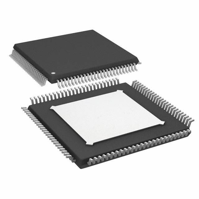
AD9271 PIN CONFIGURATION AND FUNCTION DESCRIPTIONS OSW-E O-E WD5+ WD5– WD4+ WD4– WD3+ WD3– VDD EFT EFB REF ENSE BIAS AIN+ AIN– WVDD WD2+ WD2– D1+W WD1– WD0+ WD0– O-D OSW-D L L C C C C C C A R R V S R G G C C C C C C C L L 100 99 98 97 96 95 94 93 92 91 90 89 88 87 86 85 84 83 82 81 80 79 78 77 76 LI-E 1 PIN 1 75 LI-D INDICATOR LG-E 2 74 LG-D AVDD 3 73 AVDD AVDD 4 72 AVDD LO-F 5 EXPOSED PADDLE, PIN 0 71 LO-C (BOTTOM OF PACKAGE) LOSW-F 6 70 LOSW-C LI-F 7 69 LI-C AD9271 LG-F 8 TOP VIEW 68 LG-C AVDD 9 (Not to Scale) 67 AVDD AVDD 10 66 AVDD LO-G 11 65 LO-B LOSW-G 12 64 LOSW-B LI-G 13 63 LI-B LG-G 14 62 LG-B AVDD 15 61 AVDD AVDD 16 60 AVDD LO-H 17 59 LO-A LOSW-H 18 58 LOSW-A LI-H 19 57 LI-A LG-H 20 56 LG-A AVDD 21 55 AVDD AVDD 22 54 AVDD CLK– 23 53 CSB CLK+ 24 52 SDIO AVDD 25 51 SCLK 26 27 28 29 30 31 32 33 34 35 36 37 38 39 40 41 42 43 44 45 46 47 48 49 50 DRVDD DOUTH– DOUTH+ DOUTG– DOUTG+ DOUTF– DOUTF+ DOUTE– DOUTE+ DCO– DCO+ FCO– FCO+ DOUTD– DOUTD+ DOUTC– DOUTC+ DOUTB– DOUTB+ DOUTA– DOUTA+ DRVDD STBY PDWN AVDD 06304-005 Figure 4. 100-Lead TQFP Pin Configuration Table 6. Pin Function Descriptions Pin No. Name Description 0 GND Ground (exposed paddle should be tied to a quiet analog ground) 3, 4, 9, 10, 15, AVDD 1.8 V Analog Supply 16, 21, 22, 25, 50, 54, 55, 60, 61, 66, 67, 72, 73, 92 26, 47 DRVDD 1.8 V Digital Output Driver Supply 84 CWVDD 3.3 V Analog Supply 1 LI-E LNA Analog Input for Channel E 2 LG-E LNA Ground for Channel E 5 LO-F LNA Analog Output for Channel F 6 LOSW-F LNA Analog Output Complement for Channel F 7 LI-F LNA Analog Input for Channel F 8 LG-F LNA Ground for Channel F 11 LO-G LNA Analog Output for Channel G 12 LOSW-G LNA Analog Output Complement for Channel G 13 LI-G LNA Analog Input for Channel G 14 LG-G LNA Ground for Channel G 17 LO-H LNA Analog Output for Channel H Rev. B | Page 11 of 60
AD9271 Pin No. Name Description 18 LOSW-H LNA Analog Output Complement for Channel H 19 LI-H LNA Analog Input for Channel H 20 LG-H LNA Ground for Channel H 23 CLK− Clock Input Complement 24 CLK+ Clock Input True 27 DOUTH− ADC H Digital Output Complement 28 DOUTH+ ADC H Digital Output True 29 DOUTG− ADC G Digital Output Complement 30 DOUTG+ ADC G Digital Output True 31 DOUTF− ADC F Digital Output Complement 32 DOUTF+ ADC F Digital Output True 33 DOUTE− ADC E Digital Output Complement 34 DOUTE+ ADC E Digital Output True 35 DCO− Data Clock Digital Output Complement 36 DCO+ Data Clock Digital Output True 37 FCO− Frame Clock Digital Output Complement 38 FCO+ Frame Clock Digital Output True 39 DOUTD− ADC D Digital Output Complement 40 DOUTD+ ADC D Digital Output True 41 DOUTC− ADC C Digital Output Complement 42 DOUTC+ ADC C Digital Output True 43 DOUTB− ADC B Digital Output Complement 44 DOUTB+ ADC B Digital Output True 45 DOUTA− ADC A Digital Output Complement 46 DOUTA+ ADC A Digital Output True 48 STBY Standby Power-Down 49 PDWN Full Power-Down 51 SCLK Serial Clock 52 SDIO Serial Data Input/Output 53 CSB Chip Select Bar 56 LG-A LNA Ground for Channel A 57 LI-A LNA Analog Input for Channel A 58 LOSW-A LNA Analog Output Complement for Channel A 59 LO-A LNA Analog Output for Channel A 62 LG-B LNA Ground for Channel B 63 LI-B LNA Analog Input for Channel B 64 LOSW-B LNA Analog Output Complement for Channel B 65 LO-B LNA Analog Output for Channel B 68 LG-C LNA Ground for Channel C 69 LI-C LNA Analog Input for Channel C 70 LOSW-C LNA Analog Output Complement for Channel C 71 LO-C LNA Analog Output for Channel C 74 LG-D LNA Ground for Channel D 75 LI-D LNA Analog Input for Channel D 76 LOSW-D LNA Analog Output Complement for Channel D 77 LO-D LNA Analog Output for Channel D 78 CWD0− CW Doppler Output Complement for Channel 0 79 CWD0+ CW Doppler Output True for Channel 0 80 CWD1− CW Doppler Output Complement for Channel 1 81 CWD1+ CW Doppler Output True for Channel 1 82 CWD2− CW Doppler Output Complement for Channel 2 83 CWD2+ CW Doppler Output True for Channel 2 85 GAIN− Gain Control Voltage Input Complement Rev. B | Page 12 of 60
AD9271 Pin No. Name Description 86 GAIN+ Gain Control Voltage Input True 87 RBIAS External Resistor to Set the Internal ADC Core Bias Current 88 SENSE Reference Mode Selection 89 VREF Voltage Reference Input/Output 90 REFB Differential Reference (Negative) 91 REFT Differential Reference (Positive) 93 CWD3− CW Doppler Output Complement for Channel 3 94 CWD3+ CW Doppler Output True for Channel 3 95 CWD4− CW Doppler Output Complement for Channel 4 96 CWD4+ CW Doppler Output True for Channel 4 97 CWD5− CW Doppler Output Complement for Channel 5 98 CWD5+ CW Doppler Output True for Channel 5 99 LO-E LNA Analog Output for Channel E 100 LOSW-E LNA Analog Output Complement for Channel E Rev. B | Page 13 of 60
AD9271 EQUIVALENT CIRCUITS AVDD AVDD VCM 15kΩ 350Ω LI-x, SDIO LG-x 30kΩ 06304-073 06304-008 Figure 5. Equivalent LNA Input Circuit Figure 8. Equivalent SDIO Input Circuit DRVDD AVDD V V DOUTx– DOUTx+ LO-x, 10Ω V V LOSW-x 06304-075 DRGND 06304-009 Figure 6. Equivalent LNA Output Circuit Figure 9. Equivalent Digital Output Circuit 10Ω CLK+ 10kΩ 1.25V 10kΩ 1kΩ 10Ω SCLK OR PDWN CLK– OR STBY 30kΩ 06304-007 06304-010 Figure 7. Equivalent Clock Input Circuit Figure 10. Equivalent SCLK Input Circuit Rev. B | Page 14 of 60
AD9271 AVDD 100Ω RBIAS AVDD VREF 06304-011 6kΩ 06304-014 Figure 11. Equivalent RBIAS Circuit Figure 14. Equivalent VREF Circuit AVDD 70kΩ 1kΩ CSB 50Ω GAIN+ 06304-012 06304-074 Figure 12. Equivalent CSB Input Circuit Figure 15. Equivalent GAIN+ Input Circuit 1kΩ SENSE 40kΩ GAIN– +0.5V 06304-013 06304-112 Figure 13. Equivalent SENSE Circuit Figure 16. Equivalent GAIN− Input Circuit CWDx+, 10Ω CWDx– 06304-076 Figure 17. Equivalent CWDx± Output Circuit Rev. B | Page 15 of 60
AD9271 TYPICAL PERFORMANCE CHARACTERISTICS f = 50 MSPS, f = 5 MHz, LPF = 1/3 × f , HPF = 700 kHz, LNA gain = 6×. SAMPLE IN SAMPLE 2.0 25 SAMPLE SIZE = 720 CHANNELS 1.5 20 1.0 B) %) RROR (d 0.5 +85°C UNITS ( 15 E 0 F OLUTE –0.5 –+4205°°CC CENT O 10 S R B E A –1.0 P 5 ––21..05 06304-019 0 06304-121 0 0.1 0.2 0.3 0.4 0.5 0.6 0.7 0.8 0.9 1.0 –1.0 –0.8 –0.6 –0.4 –0.2 0 0.2 0.4 0.6 0.8 1.0 VGAIN (V) GAIN ERROR (dB) Figure 18. Gain Error vs. VGAIN at Three Temperatures Figure 21. Gain Error Histogram with VGAIN = 0.9 V 20 30 SAMPLE SIZE = 720 CHANNELS 18 25 16 %) 14 %) S ( S ( 20 NIT 12 NIT U U OF 10 OF 15 T T EN 8 EN C C R R 10 E 6 E P P 4 5 02 4-1200630 0 06304-118 –1.0 –0.8 –0.6 –0.4 –0.2 0 0.2 0.4 0.6 0.8 1.0 –1.25 –1.00 –0.75 –0.50 –0.25 0 0.25 0.50 0.75 1.00 1.25 GAIN ERROR (dB) CHANNEL-TO-CHANNEL GAIN MATCHING (dB) Figure 19. Gain Error Histogram with VGAIN = 0.1 V Figure 22. Gain Match Histogram for VGAIN = 0.2 V 16 30 SAMPLE SIZE = 720 CHANNELS 14 25 PERCENT OF UNITS (%) 1120864 PERCENT OF UNITS (%) 211050 5 20 06304-116 0 06304-117 –1.0 –0.9 –0.8 –0.7 –0.6 –0.5 –0.4 –0.3G–0.2AIN–0.1 E0RR0.1OR0.2 (d0.3B)0.4 0.5 0.6 0.7 0.8 0.9 1.0 –1.25 –1C.0H0A–N0N.7E5L–-T0.O50-C–H0A.2N5NE0L GA0I.N25 MA0.T5C0HI0N.7G5 (d1B.0)0 1.25 Figure 20. Gain Error Histogram with VGAIN = 0.5 V Figure 23. Gain Match Histogram for VGAIN = 0.8 V Rev. B | Page 16 of 60
AD9271 2000000 –131 11680000000000 S/ Hz) ––113332 LNA GAIN = 8× F B 1400000 d MBER OF HITS11028000000000000000 ERRED NOISE ( –––111333654 LNA GAIN = 6× U F N E –137 600000 R T- 400000 PU –138 LNA GAIN = 5× T U 2000000 06304-022 O ––114309 06304-021 –5 –4 –3 –2 –1 0 1 2 3 4 5 0 0.1 0.2 0.3 0.4 0.5 0.6 0.7 0.8 0.9 1.0 CODES VGAIN (V) Figure 24. Output-Referred Noise Histogram with VGAIN = 0.0 V Figure 27. Short-Circuit, Output-Referred Noise vs. VGAIN 1200000 64.0 63.5 SNR (dBFS) 1000000 63.0 TS 800000 62.5 SINAD (dBFS) HI D OF NA 62.0 R 600000 SI BE NR/ 61.5 M S U N 400000 61.0 60.5 200000 0 06304-023 5690..50 06304-020 –5 –4 –3 –2 –1 0 1 2 3 4 5 0 0.1 0.2 0.3 0.4 0.5 0.6 0.7 0.8 0.9 1.0 CODES VGAIN (V) Figure 25. Output-Referred Noise Histogram with VGAIN = 1.0 V Figure 28. SNR/SINAD vs. VGAIN, AIN = −6.5 dBFS 4.5 1.70 4.0 V/ Hz) 3.5 V/ Hz) 1.65 n n E ( 3.0 E ( 1.60 S S OI OI N 2.5 N D D 1.55 E E R 2.0 R R LNA GAIN = 5× R E E F F E 1.5 LNA GAIN = 6× E 1.50 R R T- LNA GAIN = 8× T- PU 1.0 PU IN IN 1.45 0.50 06304-025 1.40 06304-024 0 5 10 15 20 25 –40 –20 0 20 40 60 80 FREQUENCY (MHz) TEMPERATURE (°C) Figure 26. Short-Circuit, Input-Referred Noise vs. Frequency Figure 29. Short-Circuit, Input-Referred Noise vs. Temperature Rev. B | Page 17 of 60
AD9271 0 –50 –5 –55 AL (dBFS) ––1150 –3dB LINE (1/3) × 40MSP(1S/3) × 50MSPS NIC (dBFS) ––6650 VGAIN = 1V NT –20 MO VGAIN = 0.5V ME AR –70 FUNDA –25 HIRD H –75 –30 (1/3) × 25MSPS T VGAIN = 0.2V ––3450 06304-030 ––8850 06304-029 0 2.5 5.0 7.5 10.0 12.5 15.0 17.5 20.0 22.5 25.0 2 4 6 8 10 12 14 16 FREQUENCY (MHz) fIN (MHz) Figure 30. Antialiasing Filter (AAF) Pass-Band Response, No HPF Applied Figure 33. Third-Order Harmonic Distortion vs. Frequency, AIN = −0.5 dBFS 300 –40 VGAIN = 0.5V 250 –50 VGAIN = 1.0V S) LAY (ns) 200 ONIC (dBF ––6700 VGAIN = 0VVGAIN = 1V UP DE 150 HARM –80 GRO 100 OND C –90 VGAIN = 0V SE 50 0 06304-033 ––111000 VGAIN = 0.5V 06304-114 0.1 1 10 100 –40 –35 –30 –25 –20 –15 –10 –5 0 ANALOG INPUT FREQUENCY (MHz) ADC OUTPUT LEVEL (dBFS) Figure 31. Antialiasing Filter (AAF) Group Delay Response Figure 34. Second-Order Harmonic Distortion vs. ADC Output Level –50 –40 –55 –50 ONIC (dBFS) ––6650 VVGGAAININ = = 0 1.2VV NIC (dBFS) ––6700 VGAIN = 1V RM MO VGAIN = 0V HA –70 AR –80 ND D H O R C –75 HI –90 SE VGAIN = 0.5V T –80 –100 –85 06304-028 –110 VGAIN = 0.5V 06304-115 2 4 6 8 10 12 14 16 –40 –35 –30 –25 –20 –15 –10 –5 0 fIN (MHz) ADC OUTPUT LEVEL (dBFS) Figure 32. Second-Order Harmonic Distortion vs. Frequency, AIN = −0.5 dBFS Figure 35. Third-Order Harmonic Distortion vs. ADC Output Level Rev. B | Page 18 of 60
AD9271 0 0 –10 AIN1 =AIN2 = –7dBFS AIN1= AIN2=–7dBFS f1= 5MHz –20 –20 IMD2=–f720=.5 69MdBHcz IMD3=–64.45dBc –30 VGAIN=1V S) –40 –40 F BFS) –50 E (dB MD3 (d –60 8MHzAND 10.3MHz LITUD –60 I –70 AMP –80 –80 –90 –100 ––110100 5MHzAND 6MHz 2.3MHzAND 3.5MHz 06304-106 –120 06304-108 0.2 0.3 0.4 0.5 0.6 0.7 0.8 0.9 1.0 0 5 10 15 20 25 VGAIN(V) FREQUENCY (MHz) Figure 36. IMD3 vs. VGAIN Figure 38. Typical IMD3 and IMD2 Performance 0 –10 f1 = 5MHz f2 = 6MHz –20 –30 –40 S) BF –50 d 3 ( –60 D M I –70 –80 VGAIN =1V VGAIN =0.5V –90 VGAIN =0V ––110100–60 –55 –50 –45 –40 –35 –30 –25 –20 –15 –10 –506304-107 INPUT AMPLITUDE (dBFS) Figure 37. IMD3 vs. Amplitude Rev. B | Page 19 of 60
AD9271 THEORY OF OPERATION ULTRASOUND following the TGC amplifier, and then beam forming is accomplished digitally. The primary application for the AD9271 is medical ultrasound. The ADC resolution of 12 bits with up to 50 MSPS sampling Figure 39 shows a simplified block diagram of an ultrasound satisfies the requirements of both general-purpose and high- system. A critical function of an ultrasound system is the time end systems. gain control (TGC) compensation for physiological signal attenuation. Because the attenuation of ultrasound signals is Power consumption and low cost are of primary importance in exponential with respect to distance (time), a linear-in-dB VGA low-end and portable ultrasound machines, and the AD9271 is is the optimal solution. designed for these criteria. Key requirements in an ultrasound signal chain are very low For additional information regarding ultrasound systems, refer noise, active input termination, fast overload recovery, low to “How Ultrasound System Considerations Influence Front-End power, and differential drive to an ADC. Because ultrasound Component Choice,” Analog Dialogue, Volume 36, Number 3, machines use beam-forming techniques requiring large binary- May–July 2002, and “The AD9271—A Revolutionary Solution weighted numbers (for example, 32 to 512) of channels, the for Portable Ultrasound,” Analog Dialogue, Volume 41, Number 7, lowest power at the lowest possible noise is of key importance. July 2007. Most modern machines use digital beam forming. In this technique, the signal is converted to digital format immediately Tx HVAMPs TxBEAM FORMER BEAM FORMER CENTRAL CONTROL MULTICHANNELS HV Rx BEAM FORMER DMEMUXU/X SWITT/CRHES LNA VGA AAF ADC (BAND F MODES) CW AD9271 TRANSDUCER ARRAY 128, 256, ETC., ELEMENTS CW (ANALOG) BIDIRECTIONAL BEAM FORMER SPECTRAL IMAGEAND COLOR CABLE DOPPLER MOTION DOPPLER (PW) PROCESSING PROCESSING PROCESSING MODE (B MODE) (F MODE) AUDIO DISPLAY OUTPUT 06304-077 Figure 39. Simplified Ultrasound System Block Diagram Rev. B | Page 20 of 60
AD9271 RFB1 LO-x gm SWTIOTCH CDWx+ ARRAY CDWx– CFB RFB2 LOSW-x T/R SWITCH CS LI-x CER CSH LNA A–3T0TdEBN TUOA T0OdBR +24dB AAF PI1PA2E-DBLCIITNE SLEVRDIASL DDOOUUTTxx+– DU CLG LG-x S N A R T GAIN INTERPOLATOR AD9271 + – N N GAI GAI 06304-071 Figure 40. Simplified Block Diagram of a Single Channel CHANNEL OVERVIEW The LNA supports differential output voltages as high as 2 V p-p with positive and negative excursions of ±0.5 V from a common- Each channel contains both a TGC signal path and a CW Doppler mode voltage of 0.9 V. The LNA differential gain sets the maximum signal path. Common to both signal paths, the LNA provides user- input signal before saturation. One of three gains is set through adjustable input impedance termination. The CW Doppler path the SPI. The corresponding input full scale for the gain settings includes a transconductance amplifier and a crosspoint switch. The of 5, 6, or 8 is 400 mV p-p, 333 mV p-p, and 250 mV p-p, TGC path includes a differential X-AMP® VGA, an antialiasing respectively. Overload protection ensures quick recovery time filter, and an ADC. Figure 40 shows a simplified block diagram from large input voltages. Because the inputs are capacitively with external components. coupled to a bias voltage near midsupply, very large inputs can The signal path is fully differential throughout to maximize be handled without interacting with the ESD protection. signal swing and reduce even-order distortion; however, the Low value feedback resistors and the current-driving capability LNA is designed to be driven from a single-ended signal source. of the output stage allow the LNA to achieve a low input-referred Low Noise Amplifier (LNA) noise voltage of 1.2 nV/√Hz. This is achieved with a current Good noise performance relies on a proprietary ultralow noise consumption of only 16 mA per channel (30 mW). On-chip LNA at the beginning of the signal chain, which minimizes the resistor matching results in precise single-ended gains, which noise contribution in the following VGA. Active impedance are critical for accurate impedance control. The use of a fully control optimizes noise performance for applications that benefit differential topology and negative feedback minimizes distortion. from input impedance matching. Low HD2 is particularly important in second-harmonic ultrasound imaging applications. Differential signaling enables smaller swings A simplified schematic of the LNA is shown in Figure 41. LI-x is at each output, further reducing third-order distortion. capacitively coupled to the source. An on-chip bias generator establishes dc input bias voltages of around 1.4 V and centers Active Impedance Matching the output common-mode levels at 0.9 V (VDD/2). A capacitor, The LNA consists of a single-ended voltage gain amplifier with C , of the same value as the input coupling capacitor, C, is LG S differential outputs and the negative output externally available. connected from the LG-x pin to ground. For example, with a fixed gain of 6× (15.6 dB), an active input CFB RFB1 termination is synthesized by connecting a feedback resistor RFB2 between the negative output pin, LO-x, and the positive input AVDD2 VO– VO+ LOSW-x pin, LI-x. This technique is well known and results in the input VCM VCM resistance shown in Equation 1: LO-x T/R SWITCHCS LI-x LG-x R = RFB (1) R IN (1+A ) UCE CSH CLG 2 D S where A/2 is the single-ended gain or the gain from the LI-x TRAN 06304-101 inputs to the LO-x outputs. Figure 41. Simplified LNA Schematic Rev. B | Page 21 of 60
AD9271 Because the amplifier has a gain of 6× from its input to its Table 7. Active Termination External Component Values differential output, it is important to note that the gain A/2 is Minimum the gain from Pin LI-x to Pin LO-x, and it is 6 dB less than the LNA Gain RIN (Ω) RFB (Ω) CSH (pF) BW (MHz) gain of the amplifier, or 9.6 dB (3×). The input resistance is 5× 50 175 90 49 reduced by an internal bias resistor of 15 kΩ in parallel with the 6× 50 200 70 59 source resistance connected to Pin LI-x, with Pin LG-x ac 8× 50 250 50 73 grounded. Equation 2 can be used to calculate the needed R 5× 100 350 30 49 FB for a desired R , even for higher values of R . 6× 100 400 20 59 IN IN 8× 100 500 10 73 R RIN =(1+FB3)||15kΩ (2) 5× 200 700 N/A 49 6× 200 800 N/A 49 For example, to set R to 200 Ω, the value of R is 845 Ω. If the IN FB 8× 200 1000 N/A 49 simplified equation (Equation 2) is used to calculate R , the IN value is 190 Ω, resulting in a gain error less than 0.5 dB. Some LNA Noise factors, such as the presence of a dynamic source resistance, might influence the absolute gain accuracy more significantly. The short-circuit noise voltage (input-referred noise) is an At higher frequencies, the input capacitance of the LNA needs important limit on system performance. The short-circuit noise to be considered. The user must determine the level of voltage for the LNA is 1.2 nV/√Hz or 1.4 nV/√Hz (at 15.6 dB matching accuracy and adjust R accordingly. LNA gain), including the VGA noise. These measurements, FB which were taken without a feedback resistor, provide the basis The bandwidth (BW) of the LNA is about 70 MHz. Ultimately for calculating the input noise and noise figure (NF) performance the BW of the LNA limits the accuracy of the synthesized R . IN of the configurations shown in Figure 43. Figure 44 and Figure 45 For R = R up to about 200 Ω, the best match is between IN S are simulations of noise figure vs. R results using these config- S 100 kHz and 10 MHz, where the lower frequency limit is urations and an input-referred noise voltage of 4 nV/√Hz for determined by the size of the ac-coupling capacitors, and the the VGA. Unterminated (R = ∞) operation exhibits the lowest FB upper limit is determined by the LNA BW. Furthermore, the equivalent input noise and noise figure. Figure 45 shows the input capacitance and R limit the BW at higher frequencies. S noise figure vs. source resistance rising at low R—where the S Figure 42 shows R vs. frequency for various values of R . IN FB LNA voltage noise is large compared with the source noise—and 1k at high R due to the noise contribution from R . The lowest S FB RS = 500Ω, RFB = 2kΩ NF is achieved when RS matches RIN. UNTERMINATED E (Ω) RS = 200Ω, RFB = 800Ω RS RIN C N + DA RS = 100Ω, RFB = 400Ω, CSH = 20pF VIN VOUT E 100 – P M UT I RS = 50Ω, RFB = 200Ω, CSH = 70pF RESISTIVE TERMINATION P IN RIN RS 10 06304-105 VIN+– RS VOUT 100k 1M 10M 50M FREQUENCY (Hz) ACTIVE IMPEDANCE MATCH Figure 42. RIN vs. Frequency for Various Values of RFB RIN RFB (Effects of RSH and CSH Are Also Shown) RS + Note that at the lowest value, 50 Ω, in Figure 42, RIN peaks at VIN VOUT frequencies greater than 10 MHz. This is due to the BW roll-off – oHfo twheev LeNr, Aas, caasn m been steieonn efodr plarregveiro RusINly v. alues, parasitic capacitance RIN=1 R+ FAB/2 06304-104 starts rolling off the signal BW before the LNA can produce Figure 43. Input Configurations peaking. C further degrades the match; therefore, C should SH SH not be used for values of R that are greater than 100 Ω. Table 7 IN lists the recommended values for R and C in terms of R . FB SH IN C is needed in series with R because the dc levels at Pin LO-x FB FB and Pin LI-x are unequal. Rev. B | Page 22 of 60
AD9271 16 INPUT OVERDRIVE 14 Excellent overload behavior is of primary importance in ultra- UNTERMINATED sound. Both the LNA and VGA have built-in overdrive 12 protection and quickly recover after an overload event. B) RESISTIVE TERMINATION E (d 10 ACTIVE TERMINATION Input Overload Protection R U G 8 As with any amplifier, voltage clamping prior to the inputs is FI OISE 6 highly recommended if the application is subject to high N transient voltages. 4 A block diagram of a simplified ultrasound transducer interface 02 06304-103 idsu sahl ofwunnc itnio Fnisg oufr et r4a6n.s Am ictotimngm aonnd trreacnesidvuincge ru eltlreamsoenutn sde ervneesr gthy.e 10 100 1000 During the transmitting phase, high voltage pulses are applied RS(Ω) to the ceramic elements. A typical transmit/receive (T/R) switch Figure 44. Noise Figure vs. RS for Resistive Termination, Active Termination can consist of four high voltage diodes in a bridge configuration. Matched, and Unterminated Inputs, VGain = 1 V, 15.6 dB LNA Gain Although the diodes ideally block transmit pulses from the 16 sensitive receiver input, diode characteristics are not ideal, and 14 resulting leakage transients imposed on the LI-x inputs can be problematic. 12 RIN = 50Ω B) Because ultrasound is a pulse system and time-of-flight is used E (d 10 RIN = 75Ω to determine depth, quick recovery from input overloads is R U FIG 8 RIN = 100Ω essential. Overload can occur in the preamp and the VGA. E Immediately following a transmit pulse, the typical VGA gains OIS 6 are low, and the LNA is subject to overload from T/R switch N 4 leakage. With increasing gain, the VGA can become overloaded due to strong echoes that occur near field echoes and 02 RINU =N T20E0RΩMINATED 06304-102 acoustically dense materials, such as bone. 10 100 1000 Figure 46 illustrates an external overload protection scheme. A RS(Ω) pair of back-to-back Schottky diodes is installed prior to installing Figure 45. Noise Figure vs. RS for Various Fixed Values of RIN, the ac-coupling capacitors. Although the BAS40 diodes are shown, Active Termination Matched Inputs, VGain = 1 V, 15.6 dB LNA Gain any diode is prone to exhibiting some amount of shot noise. Many The primary purpose of input impedance matching is to improve types of diodes are available for achieving the desired noise per- the transient response of the system. With resistive termination, the formance. The configuration shown in Figure 46 tends to add input noise increases due to the thermal noise of the matching 2 nV/√Hz of input-referred noise. Decreasing the 5 kΩ resistor resistor and the increased contribution of the LNA’s input and increasing the 2 kΩ resistor may improve noise contribution, voltage noise generator. With active impedance matching, depending on the application. With the diodes shown in Figure 46, however, the contributions of both are smaller (by a factor of clamping levels of ±0.5 V or less significantly enhance the 1/(1 + LNA Gain)) than they would be for resistive termination. overload performance of the system. Figure 44 shows the relative noise figure performance. In this +5V graph, the input impedance was swept with R to preserve the S Tx 5kΩ match at each point. The noise figures for a source impedance of DRIVER HV AD9271 50 Ω are 7.1 dB, 4.1 dB, and 2.5 dB for the resistive termination, BAS40-04 10nF active termination, and unterminated configurations, respectively. LNA The noise figures for 200 Ω are 4.6 dB, 2.0 dB, and 1.0 dB, 2kΩ 5kΩ 10nF rFeigspuercet 4iv5e slyh.o ws the noise figure as it relates to RS for various values TRANSDUCER –5V 06304-100 of R , which is helpful for design purposes. Figure 46. Input Overload Protection IN Rev. B | Page 23 of 60
AD9271 CW DOPPLER OPERATION gain, and it defines a focal point within the body from which the location of the returning echo is derived. Modern ultrasound machines used for medical applications employ a 2N binary array of receivers for beam forming, with The AD9271 includes the front-end components needed to typical array sizes of 16 or 32 receiver channels phase-shifted implement analog beam forming for CW Doppler operation. and summed together to extract coherent information. When These components allow CW channels with similar phases to be used in multiples, the desired signals from each channel can be coherently combined before phase alignment and down mixing, summed to yield a larger signal (increased by a factor N, where thus reducing the number of delay lines or adjustable phase shifters/ N is the number of channels), and the noise is increased by the down mixers (AD8333 or AD8339) required. Next, if delay lines square root of the number of channels. This technique enhances are used, the phase alignment is performed and then the channels the signal-to-noise performance of the machine. The critical are coherently summed and down converted by a dynamic range elements in a beam-former design are the means to align the I/Q demodulator. Alternatively, if phase shifters/down mixers, incoming signals in the time domain and the means to sum the such as the AD8333 and AD8339, are used, phase alignment individual signals into a composite whole. and downconversion are done before coherently summing all channels into I/Q signals. In either case, the resultant I and Q Beam forming, as applied to medical ultrasound, is defined as the signals are filtered and sampled by two high resolution ADCs, phase alignment and summation of signals that are generated and the sampled signals are processed to extract the relevant from a common source but received at different times by a Doppler information. multielement ultrasound transducer. Beam forming has two functions: it imparts directivity to the transducer, enhancing its AD9271 LNA gm LNA gm SWITCH 8 × CHANNEL ARRAY AD8333 600nH LNA gm 2.5V 700Ω 600nH LNA gm 600nH 2.5V 700Ω 600nH AD8333 AD9271 600nH 2.5V 700Ω LNA gm 600nH LNA gm 600nH 2.5V 700Ω 600nH SWITCH ARRAY I 8 × CHANNEL 16-BIT ADC LNA gm LNA gm Q 1A6-DBCIT 06304-096 Figure 47. Typical CW Doppler System Using the AD9271 and AD8333 or AD8339 Rev. B | Page 24 of 60
AD9271 Crosspoint Switch The system gain is distributed as listed in Table 8. Each LNA is followed by a transconductance amp for V/I con- Table 8. Channel Gain Distribution version. Currents can be routed to one of six pairs of differential Section Nominal Gain (dB) outputs or to 12 single-ended outputs for summing. Each CWD LNA 14/15.6/18 output pin sinks 2.4 mA dc current, and the signal has a full-scale Attenuator 0 to −30 current of ±2 mA for each channel selected by the crosspoint VGA Amp 24 switch. For example, if four channels were to be summed on Filter 0 one CWD output, the output would sink 9.6 mA dc and have a ADC 0 full-scale current output of ±8 mA. The maximum number of Total 8.4 to 38.4/10 to 40/12.4 to 42.4 channels combined must be considered when setting the load impedance for I/V conversion to ensure that the full-scale swing and common-mode voltage are within the operating limits of The linear-in-dB gain (law conformance) range of the TGC path the AD9271. When interfacing to the AD8339, a common- is 30 dB, extending from 10 dB to 40 dB. The slope of the gain mode voltage of 2.5 V and a full-scale swing of 2.8 V p-p are control interface is 31.6 dB/V, and the gain control range is 0 V desired. This can be accomplished by connecting an inductor to 1 V as specified in Equation 3. Equation 4 is the expression between each CWD output and a 2.5 V supply, and then for channel gain. connecting either a single-ended or differential load resistance V (V)=(GAIN+)−(GAIN−)+0.5 (3) GAIN to the CWD± outputs. The value of resistance should be calculated based on the maximum number of channels that can Gain(dB)=31.6dBV +ICPT (4) V GAIN be combined. where ICPT is the intercept point of the TGC gain. CWD± outputs are required under full-scale swing to be greater In its default condition, the LNA has a gain of 15.6 dB (6×) and than 1.5 V and less than CWVDD (3.3 V supply). the VGA gain is −6 dB if the voltage on the GAIN± pins is 0 V. TGC OPERATION This gives rise to a total gain (or ICPT) of 10 dB through the The TGC signal path is fully differential throughout to maximize TGC path if the LNA input is unmatched, or of 4 dB if the LNA signal swing and reduce even-order distortion; however, the LNAs is matched to 50 Ω (R = 200 Ω). If the voltage on the GAIN± FB are designed to be driven from a single-ended signal source. Gain pins is 1 V, however, the VGA gain is 24 dB. This gives rise to a values are referenced from the single-ended LNA input to the total gain of 40 dB through the TGC path if the LNA input is differential ADC input. A simple exercise in understanding the unmatched, or of 34 dB if the LNA input is matched. maximum and minimum gain requirements is shown in Figure 48. Each LNA output is dc-coupled to a VGA input. The VGA consists of an attenuator with a range of 30 dB followed by an amplifier ADCFS(2Vp-p) with 24 dB of gain for a net gain range of −6 dB to +24 dB. The MINIMUM GAIN ~5dBMARGIN X-AMP gain-interpolation technique results in low gain error (0.333VLpN-pA S FES) 70dB ADC and uniform bandwidth, and differential signal paths minimize distortion. 87dB >8dBMARGIN At low gains, the VGA should limit the system noise perfor- LNA ADC NOISE FLOOR (224µVrms) mance (SNR); at high gains, the noise is defined by the source and MAXIMUM GAIN LNA. The maximum voltage swing is bound by the full-scale LNA INPUT-REFERRED NOISE FLOOR peak-to-peak ADC input voltage (2 V p-p). (5L.4NµAV+rmVsG)A @ NAOAISFEB=W1.=4n1V5M/ HHzz VMGAAX GCHAAINN RNAENL GGEA I>N 3 >0 d4B0dB 06304-097 Both the LNA and VGA have limitations within each section of Figure 48. Gain Requirements of TGC for a 12-Bit, 40 MSPS ADC the TGC path, depending on the voltage applied to the GAIN+ and GAIN− pins. The LNA has three limitations, or full-scale settings, In summary, the maximum gain required is determined by depending on the gain selection applied through the SPI interface. (ADC Noise Floor/VGA Input Noise Floor) + Margin = When a voltage of 0.2 V or less is applied to the GAIN± pins, the 20 log(224/5.4) + 8 dB = 40.3 dB LNA operates near the full-scale input range to maximize the The minimum gain required is determined by dynamic range of the ADC without clipping the signal. When more than 0.2 V is applied to the GAIN± pins, the input signal to (ADC Input FS/VGA Input FS) + Margin = the LNA must be lowered to keep it within the full-scale range 20 log(2/0.333) – 5 dB = 10.6 dB of the ADC (see Figure 49). Therefore, a 12-bit, 40 MSPS ADC with 15 MHz of bandwidth should suffice in achieving the dynamic range required for most of today’s ultrasound systems. Rev. B | Page 25 of 60
AD9271 0.450 slope is monotonic with respect to the control voltage and is LNA GAIN = 5x 0.400 stable with variations in process, temperature, and supply. p) 0.350 The X-AMP inputs are part of a 24 dB gain feedback amplifier p- that completes the VGA. Its bandwidth is about 70 MHz. The V 0.300 LNA E ( GAIN = 6x input stage is designed to reduce feedthrough to the output and L CA 0.250 to ensure excellent frequency response uniformity across the S LL- 0.200 LNA GAIN = 8x gain setting. U F T 0.150 Gain Control U P IN 0.100 The gain control interface, GAIN±, is a differential input. The VGA gain, V , is shown in Equation 3. V varies the gain 0.05000 0.1 0.2 0.3 0.4 0.5 0.6 0.7 0.8 0.9 1.006304-110 oinf paullt V sGtaAgess t hcGorAonINungehc ttehde tinot tehrpe oilnaptourt baytt seenleucattiGonArgI.N tThhee a pnpormopinriaalt e VGAIN (V) VGAIN range for 30 dB/V is 0 V to 1 V, with the best gain linearity Figure 49. LNA/VGA Full-Scale Limitations from about 0.1 V to 0.9 V, where the error is typically less than Variable Gain Amplifier ±0.5 dB. For VGAIN voltages greater than 0.9 V and less than 0.1 V, the error increases. The value of V can exceed the supply GAIN The differential X-AMP VGA provides precise input attenuation voltage by 1 V without gain foldover. and interpolation. It has a low input-referred noise of 4 nV/√Hz and excellent gain linearity. A simplified block diagram is shown Gain control response time is less than 750 ns to settle within 10% in Figure 50. of the final value for a change from minimum to maximum gain. There are two ways in which the GAIN+ and GAIN− pins can GAIN GAININTERPOLATOR be interfaced. Using a single-ended method, a Kelvin type of POSTAMP + connection to ground can be used as shown in Figure 51. For gm driving multiple devices, it is preferable to use a differential 3dB method, as shown in Figure 52. In either method, the GAIN+ VIP and GAIN− pins should be dc-coupled and driven to accom- modate a 1 V full-scale input. VIN AD9271 100Ω GAIN+ 0 TO 1V DC 0.01µF 50Ω – POSTAMP 06304-078 GAIN– 0.01µF CONKNELEVCITNION 06304-109 Figure 50. Simplified VGA Schematic Figure 51. Single-Ended GAIN± Pins Configuration The input of the VGA is a 12-stage differential resistor ladder with 499Ω AVDD 3.01 dB per tap. The resulting total gain range is 30 dB, which AD9271 ±0.25DC AT 26kΩ allows for range loss at the endpoints. The effective input resistance 100Ω 0.5V CM 499Ω GAIN+ ±0.5V DC per side is 180 Ω nominally for a total differential resistance of 0.01µF AD8138 0.5V CM 50Ω 360 Ω. The ladder is driven by a fully differential input signal from 100Ω 523Ω GAIN– ±0.25DC AT 10kΩ tcVhaGep aALcN iitsAo c.r osL.nN TtArho eol lcueodtpm bumyts aoannre -a mdmcop-dcloiefu iveporl lettdhag ateot uoafsv eothsid et h eaextt tseeanrmnuaaelt omdre icadonsudup ptlpihnleyg 0.01µF 0.5V CM 499Ω 06304-098 Figure 52. Differential GAIN± Pins Configuration voltage derived in the LNA, permitting dc coupling of the LNA VGA Noise to the VGA without introducing large offsets due to common- mode differences. However, any offset from the LNA will be In a typical application, a VGA compresses a wide dynamic amplified as the gain is increased, producing an exponentially range input signal to within the input span of an ADC. The increasing VGA output offset. input-referred noise of the LNA limits the minimum resolvable input signal, whereas the output-referred noise, which depends The input stages of the X-AMP are distributed along the ladder, primarily on the VGA, limits the maximum instantaneous and a biasing interpolator, controlled by the gain interface, dynamic range that can be processed at any one particular gain determines the input tap point. With overlapping bias currents, control voltage. This latter limit is set in accordance with the signals from successive taps merge to provide a smooth total noise floor of the ADC. attenuation range from 0 dB to −30 dB. This circuit technique results in linear-in-dB gain law conformance and low distortion Output-referred noise as a function of VGAIN is shown in Figure 24 levels—only deviating ±0.5 dB or less from the ideal. The gain and Figure 25 for the short-circuit input conditions. The input Rev. B | Page 26 of 60
AD9271 noise voltage is simply equal to the output noise divided by the The filter can be configured for dc coupling or to have a single measured gain at each point in the control range. pole for high-pass filtering at either 700 kHz or 350 kHz (programmed through the SPI). The high-pass pole, however, is The output-referred noise is a flat 63 nV/√Hz over most of the not tuned and can vary by ±30%. gain range, because it is dominated by the fixed output-referred noise of the VGA. At the high end of the gain control range, the A third-order Butterworth low-pass filter is used to reduce noise of the LNA and source prevail. The input-referred noise noise bandwidth and provide antialiasing for the ADC. The reaches its minimum value near the maximum gain control filter uses on-chip tuning to trim the capacitors and in turn set voltage, where the input-referred contribution of the VGA is the desired cutoff frequency and reduce variations. The default miniscule. −3 dB cutoff is 1/3 the ADC sample clock rate. The cutoff can be scaled to 0.7, 0.8, 0.9, 1, 1.1, 1.2, or 1.3 times this frequency At lower gains, the input-referred noise and, therefore, the noise through the SPI. The cutoff can be set from 8 MHz to 18 MHz. figure increases as the gain decreases. The instantaneous dynamic range of the system is not lost, however, because the input capacity Tuning is normally off to avoid changing the capacitor settings increases as the input-referred noise increases. The contribution during critical times. The tuning circuit is enabled and disabled of the ADC noise floor has the same dependence. The important through the SPI. Initializing the tuning of the filter must be relationship is the magnitude of the VGA output noise floor done after initial power-up and after reprogramming the filter relative to that of the ADC. cutoff scaling or ADC sample rate. Occasional retuning during an idle time is recommended to compensate for temperature drift. Gain control noise is a concern in very low noise applications. Thermal noise in the gain control interface can modulate the ADC channel gain. The resultant noise is proportional to the output The AD9271 architecture consists of a pipelined ADC divided signal level and is usually evident only when a large signal is into three sections: a 4-bit first stage followed by eight 1.5-bit present. The gain interface includes an on-chip noise filter, which stages and a 3-bit flash. Each stage provides sufficient overlap to significantly reduces this effect at frequencies above 5 MHz. Care correct for flash errors in the preceding stages. The quantized should be taken to minimize noise impinging at the GAIN± outputs from each stage are combined into a 12-bit result in the input. An external RC filter can be used to remove V source GAIN digital correction logic. The pipelined architecture permits the noise. The filter bandwidth should be sufficient to accommodate first stage to operate on a new input sample and the remaining the desired control bandwidth. stages to operate on preceding samples. Sampling occurs on the Antialiasing Filter rising edge of the clock. The filter that the signal reaches prior to the ADC is used to Each stage of the pipeline except for the last consists of a low reject dc signals and to band limit the signal for antialiasing. resolution flash ADC connected to a switched-capacitor DAC Figure 53 shows the architecture of the filter. and interstage residue amplifier (for example, a multiplying 4kΩ digital-to-analog converter (MDAC)). The residue amplifier magnifies the difference between the reconstructed DAC output 1C* and the flash input for the next stage in the pipeline. One bit of 56pF/112pF redundancy is used in each stage to facilitate digital correction 2kΩ 2kΩ 2kΩ of flash errors. The last stage consists of a flash ADC. 7.5C* 6.5C* The output staging block aligns the data, carries out error cor- 2kΩ 2kΩ 2kΩ rection, and passes the data to the output buffers. The data is then serialized and aligned to the frame and output clock. 56pF/112pF 1C* *C = 0.5pF TO 3.1pF 4kΩ 06304-099 Figure 53. Simplified Filter Schematic Rev. B | Page 27 of 60
AD9271 CLOCK INPUT CONSIDERATIONS In some applications, it is acceptable to drive the sample clock inputs with a single-ended CMOS signal. In such applications, For optimum performance, the AD9271 sample clock inputs CLK+ should be driven directly from a CMOS gate, and the (CLK+ and CLK−) should be clocked with a differential signal. CLK− pin should be bypassed to ground with a 0.1 μF capacitor This signal is typically ac-coupled into the CLK+ and CLK− pins in parallel with a 39 kΩ resistor (see Figure 57). Although the via a transformer or capacitors. These pins are biased internally CLK+ input circuit supply is AVDD (1.8 V), this input is and require no additional bias. designed to withstand input voltages of up to 3.3 V, making the Figure 54 shows the preferred method for clocking the AD9271. selection of the drive logic voltage very flexible. A low jitter clock source, such as the Valpey Fisher oscillator 3.3V VFAC3-BHL-50MHz, is converted from single-ended to AD951x FAMILY differential using an RF transformer. The back-to-back Schottky VFAC3 0.1µF OUT CLK diodes across the secondary transformer limit clock excursions EN 50Ω* OP1T0IO0ΩNAL0.1µF into the AD9271 to approximately 0.8 V p-p differential. This CMOS DRIVER CLK+ ADC helps prevent the large voltage swings of the clock from feeding CLK AD9271 through to other portions of the AD9271, and it preserves the 0.1µF CLK– fast rise and fall times of the signal, which are critical to low 0.1µF 39kΩ jitter performance. *50Ω RESISTOR IS OPTIONAL. 06304-053 3.3V Figure 57. Single-Ended 1.8 V CMOS Sample Clock MINI-CIRCUITS ADT1-1WT, 1:1Z 3.3V 0.1µF XFMR 0.1µF AD951x FAMILY ENOUT CLK+ 0.1µF 50Ω 100Ω ADC OUT CLK VFAC3 0.1µF AD9271 EN 50Ω* OP1T0IO0ΩNAL 0.1µF CLK– CMOS DRIVER CLK+ 0.1µF SHCDSHIOMOD2TE8T1SK2:Y 06304-050 VFAC3 0.1µF CLK 0.1µF ADA9D2C71 If a low jitteFri gculorec 5k4 .i sT raavnasfiolarmbleer,- Caonuoptlheedr D oifpfetrieonnti aisl Ctloo cakc -couple a *50Ω RESISTOR IS OPTIONAL. CLK– 06304-054 Figure 58. Single-Ended 3.3 V CMOS Sample Clock differential PECL signal to the sample clock input pins as shown in Figure 55. The AD951x family of clock drivers offers excellent Clock Duty Cycle Considerations jitter performance. Typical high speed ADCs use both clock edges to generate a variety of internal timing signals. As a result, these ADCs may 3.3V 50Ω* AD951x FAMILY be sensitive to the clock duty cycle. Commonly, a 5% tolerance is VFAC3 0.1µF 0.1µF OUT CLK CLK+ required on the clock duty cycle to maintain dynamic performance EN ADC characteristics. The AD9271 contains a duty cycle stabilizer (DCS) 0.1µF PECL DRIVER 100.01ΩµF AD9271 that retimes the nonsampling edge, providing an internal clock CLK CLK– signal with a nominal 50% duty cycle. This allows a wide range 240Ω 240Ω of clock input duty cycles without affecting the performance of *50Ω RESISTOR IS OPTIONAL. 06304-051 the AD9271. When the DCS is on, noise and distortion perfor- Figure 55. Differential PECL Sample Clock mance are nearly flat for a wide range of duty cycles. However, some applications may require the DCS function to be off. If so, 3.3V keep in mind that the dynamic range performance can be affected 50Ω* AD951x FAMILY VFAC3 0.1µF 0.1µF when operated in this mode. See the Memory Map section for OUT CLK CLK+ more details on using this feature. EN ADC LVDS DRIVER 100Ω AD9271 The duty cycle stabilizer uses a delay-locked loop (DLL) to 0.1µF 0.1µF CLK CLK– create the nonsampling edge. As a result, any changes to the sampling frequency require approximately eight clock cycles *50Ω RESISTOR IS OPTIONAL. 06304-052 tCol oalclkow Ji tthteer D CLoLn tsoi daecqrautirieo nansd lock to the new rate. Figure 56. Differential LVDS Sample Clock High speed, high resolution ADCs are sensitive to the quality of the clock input. The degradation in SNR at a given input frequency (f ) A due only to aperture jitter (t) can be calculated by J SNR Degradation = 20 × log 10[1/2 × π × f × t] A J Rev. B | Page 28 of 60
AD9271 In this equation, the rms aperture jitter represents the root mean 190 square of all jitter sources, including the clock input, analog input 180 signal, and ADC aperture jitter. IF undersampling applications 170 are particularly sensitive to jitter (see Figure 59). W) 50MSPS SPEED GRADE m 160 The clock input should be treated as an analog signal in cases L ( E where aperture jitter may affect the dynamic range of the AD9271. NN 150 A Power supplies for clock drivers should be separated from the CH 140 R/ 40MSPS SPEED GRADE ADC output driver supplies to avoid modulating the clock signal E W 130 with digital noise. Low jitter, crystal-controlled oscillators make O P the best clock sources, such as the Valpey Fisher VFAC3 series. 120 25MSPS SPEED GRADE Idfi vthidei nclgo,c okr ios tgheenre mraetethdo fdros)m, i ta nshoothueldr tbyep ree otifm soedu rbcye t(hbey gating, 110100 06304-031 original clock during the last step. 0 10 20 30 40 50 SAMPLING FREQUENCY (MSPS) Refer to the AN-501 Application Note and the AN-756 Figure 61. Power per Channel vs. fSAMPLE for fIN = 7.5 MHz Application Note for more in-depth information about how By asserting the PDWN pin high, the AD9271 is placed into jitter performance relates to ADCs (visit www.analog.com). power-down mode. In this state, the device typically dissipates 130 RMS CLOCK JITTER REQUIREMENT 2 mW. During power-down, the LVDS output drivers are placed 120 into a high impedance state. The AD9271 returns to normal 110 operating mode when the PDWN pin is pulled low. This pin is 100 16 BITS both 1.8 V and 3.3 V tolerant. B) 90 14 BITS By asserting the STBY pin high, the AD9271 is placed into a SNR (d 7800 12 BITS s6t5a nmdWby. Dmuordine.g I nst athnidsb syt,a tthe,e t ehnet direev picaer tt yisp ipcoawllye rdeids sdipoawtens except 10 BITS the internal references. The LVDS output drivers are placed into 60 0.125ps a high impedance state. This mode is well suited for applications 8 BITS 50 0.25ps that require power savings because it allows the device to be 0.5ps 40 1.0ps powered down when not in use and then quickly powered up. 2.0ps 30 The time to power the device back up is also greatly reduced. The 1 ANALO1G0 INPUT FREQUENC10Y0 (MHz) 1000 06304-038 Ais Dpu92ll7e1d rleotwu.r Tnsh tios pnionr mis ablo otphe 1r.a8t iVng a mndo d3e.3 w Vh etonl ethraen St.T BY pin Figure 59. Ideal SNR vs. Input Frequency and Jitter Power Dissipation and Power-Down Mode In power-down mode, low power dissipation is achieved by shutting down the reference, reference buffer, PLL, and biasing As shown in Figure 61, the power dissipated by the AD9271 is networks. The decoupling capacitors on REFT and REFB are proportional to its sample rate. The digital power dissipation discharged when entering power-down mode and must be does not vary much because it is determined primarily by the recharged when returning to normal operation. As a result, the DRVDD supply and bias current of the LVDS output drivers wake-up time is related to the time spent in the power-down (Figure 60). mode: shorter cycles result in proportionally shorter wake-up 800 times. To restore the device to full operation, approximately 700 IAVDD, 50MSPS SPEED GRADE 1 ms is required when using the recommended 0.1 μF and 4.7 μF decoupling capacitors on the REFT and REFB pins and the 600 IAVDD, 40MSPS SPEED GRADE 0.01 μF decoupling capacitors on the GAIN± pins. Most of this A) 500 time is dependent on the gain decoupling; higher value decoupling T (m IAVDD, 25MSPS SPEED GRADE capacitors on the GAIN± pins result in longer wake-up times. N 400 E R There are a number of other power-down options available R CU 300 when using the SPI port interface. The user can individually power down each channel or put the entire device into standby 200 mode. This allows the user to keep the internal PLL powered up 1000 IDRVDD 3206304-0 wslihgehntl fya dste wpeankde-eunpt otinm geasi nar. eT ore aqcuhirieevde. Ta h1e μ ws awkaek-eu-pu pti mtime ies 0 10 20 30 40 50 when the device is in standby mode, 0.5 V must be applied to SAMPLING FREQUENCY (MSPS) the GAIN± pins. See the Memory Map section for more details Figure 60. Supply Current vs. fSAMPLE for fIN = 7.5 MHz on using these features. Rev. B | Page 29 of 60
AD9271 Digital Outputs and Timing Additional SPI options allow the user to further increase the internal termination (and therefore increase the current) of all The AD9271 differential outputs conform to the ANSI-644 LVDS eight outputs in order to drive longer trace lengths (see Figure 65). standard on default power-up. This can be changed to a low power, Even though this produces sharper rise and fall times on the reduced signal option similar to the IEEE 1596.3 standard by using data edges, is less prone to bit errors, and improves frequency the SDIO pin or via the SPI. This LVDS standard can further distribution (see Figure 65), the power dissipation of the DRVDD reduce the overall power dissipation of the device by approximately supply increases when this option is used. 36 mW. See the SDIO Pin section or Table 15 for more information. In cases that require increased driver strength to the DCO± and FCO± outputs because of load mismatch, Register 0x15 allows The LVDS driver current is derived on chip and sets the output the user to double the drive strength. To do this, first set the current at each output equal to a nominal 3.5 mA. A 100 Ω differ- appropriate bit in Register 0x05. Note that this feature cannot ential termination resistor placed at the LVDS receiver inputs be used with Bit 4 and Bit 5 in Register 0x15 because these bits results in a nominal 350 mV swing at the receiver. take precedence over this feature. See the Memory Map section The AD9271 LVDS outputs facilitate interfacing with LVDS for more details. receivers in custom ASICs and FPGAs that have LVDS capability 600 for superior switching performance in noisy environments. EYE: ALL BITS ULS: 2398/2398 Single point-to-point net topologies are recommended with a 400 100 Ω termination resistor placed as close to the receiver as possible. No far-end receiver termination and poor differential E (V) 200 G trace routing may result in timing errors. It is recommended TA 100 L that the trace length be no longer than 24 inches and that the VO M 0 differential output traces be kept close together and at equal A R lengths. An example of the FCO, DCO, and data stream with AG –100 DI proper trace length and position can be found in Figure 62. E Y –200 E –400 –600 –1.5ns –1.0ns –0.5ns 0ns 0.5ns 1.0ns 1.5ns 25 s) 20 Hit M ( A R 15 G O 06304-034 R HIST 10 CH1 500mV/DIV Ω 5.0ns/DIV E CH2 500mV/DIV Ω TT CH3 500mV/DIV Ω JI E Figure 62. LVDS Output Timing Example in ANSI-644 Mode (Default) TI 5 A(dne feaxualtm) dplaet ao ef ythe ea nLdV Da tSi moue tipnutet ruvsailn egr rthoer (ATNIES)I -ji6t4te4r shtiasntodgarradm 0 06304-035 –200ps –100ps 0ps 100ps 200ps with trace lengths of less than 24 inches on regular FR-4 material Figure 63. Data Eye for LVDS Outputs in ANSI-644 Mode with Trace Lengths is shown in Figure 63. Figure 64 shows an example of the trace of Less Than 24 Inches on Standard FR-4 lengths exceeding 24 inches on regular FR-4 material. Notice that the TIE jitter histogram reflects the decrease of the data eye opening as the edge deviates from the ideal position; therefore, the user must determine if the waveforms meet the timing budget of the design when the trace lengths exceed 24 inches. Rev. B | Page 30 of 60
AD9271 400 600 EYE: ALL BITS ULS: 2399/2399 EYE: ALL BITS ULS: 2396/2396 300 400 E (V) 200 E (V) AG AG 200 OLT 100 OLT V V M 0 M 0 A A R R G G A –100 A DI DI –200 E E EY –200 EY –400 –300 –400 –600 –1.5ns –1.0ns –0.5ns 0ns 0.5ns 1.0ns 1.5ns –1.5ns –1.0ns –0.5ns 0ns 0.5ns 1.0ns 1.5ns 25 25 Hits) 20 Hits) 20 M ( M ( A A R 15 R 15 G G O O ST ST HI HI R 10 R 10 E E E JITT E JITT TI 5 TI 5 0 06304-036 0 06304-037 –200ps –100ps 0ps 100ps 200ps –200ps –100ps 0ps 100ps 200ps Figure 64. Data Eye for LVDS Outputs in ANSI-644 Mode with Trace Lengths Figure 65. Data Eye for LVDS Outputs in ANSI-644 Mode with 100 Ω of Greater Than 24 Inches on Standard FR-4 Termination On and Trace Lengths of Greater Than 24 Inches on Standard FR-4 Rev. B | Page 31 of 60
AD9271 The format of the output data is offset binary by default. An times the sample clock rate, with a maximum of 600 Mbps example of the output coding format can be found in Table 9. (12 bits × 50 MSPS = 600 Mbps). The lowest typical conversion To change the output data format to twos complement, see the rate is 10 MSPS, but the PLL can be set up for encode rates as Memory Map section. low as 5 MSPS via the SPI if lower sample rates are required for a specific application. See the Memory Map section for details Table 9. Digital Output Coding on enabling this feature. (VIN+) − (VIN−), Digital Output Offset Binary Code Input Span = 2 V p-p (V) (D11 ... D0) Two output clocks are provided to assist in capturing data from the AD9271. DCO± is used to clock the output data and is equal 4095 +1.00 1111 1111 1111 to six times the sampling clock rate. Data is clocked out of the 2048 0.00 1000 0000 0000 AD9271 and must be captured on the rising and falling edges of 2047 −0.000488 0111 1111 1111 the DCO± that supports double data rate (DDR) capturing. The 0 −1.00 0000 0000 0000 frame clock output (FCO±) is used to signal the start of a new Data from each ADC is serialized and provided on a separate output byte and is equal to the sampling clock rate. See the channel. The data rate for each serial stream is equal to 12 bits timing diagram shown in Figure 2 for more information. Table 10. Flexible Output Test Modes Output Test Mode Subject to Data Bit Sequence Pattern Name Digital Output Word 1 Digital Output Word 2 Format Select 0000 Off (default) N/A N/A N/A 0001 Midscale short 1000 0000 (8 bits) Same Yes 10 0000 0000 (10 bits) 1000 0000 0000 (12 bits) 10 0000 0000 0000 (14 bits) 0010 +Full-scale short 1111 1111 (8 bits) Same Yes 11 1111 1111 (10 bits) 1111 1111 1111 (12 bits) 11 1111 1111 1111 (14 bits) 0011 −Full-scale short 0000 0000 (8 bits) Same Yes 00 0000 0000 (10 bits) 0000 0000 0000 (12 bits) 00 0000 0000 0000 (14 bits) 0100 Checkerboard 1010 1010 (8 bits) 0101 0101 (8 bits) No 10 1010 1010 (10 bits) 01 0101 0101 (10 bits) 1010 1010 1010 (12 bits) 0101 0101 0101 (12 bits) 10 1010 1010 1010 (14 bits) 01 0101 0101 0101 (14 bits) 0101 PN sequence long1 N/A N/A Yes 0110 PN sequence short1 N/A N/A Yes 0111 One-/zero-word toggle 1111 1111 (8 bits) 0000 0000 (8 bits) No 11 1111 1111 (10 bits) 00 0000 0000 (10 bits) 1111 1111 1111 (12 bits) 0000 0000 0000 (12 bits) 11 1111 1111 1111 (14 bits) 00 0000 0000 0000 (14 bits) 1000 User input Register 0x19 and Register 0x1A Register 0x1B and Register 0x1C No 1001 1-/0-bit toggle 1010 1010 (8 bits) N/A No 10 1010 1010 (10 bits) 1010 1010 1010 (12 bits) 10 1010 1010 1010 (14 bits) 1010 1× sync 0000 1111 (8 bits) N/A No 00 0001 1111 (10 bits) 0000 0011 1111 (12 bits) 00 0000 0111 1111 (14 bits) 1011 One bit high 1000 0000 (8 bits) N/A No 10 0000 0000 (10 bits) 1000 0000 0000 (12 bits) 10 0000 0000 0000 (14 bits) 1100 Mixed bit frequency 1010 0011 (8 bits) N/A No 10 0110 0011 (10 bits) 1010 0011 0011 (12 bits) 10 1000 0110 0111 (14 bits) 1 All test mode options except PN sequence short and PN sequence long can support 8- to 14-bit word lengths in order to verify data capture to the receiver. Rev. B | Page 32 of 60
AD9271 When using the serial port interface (SPI), the DCO± phase can SDIO Pin be adjusted in 60° increments relative to the data edge. This This pin is required to operate the SPI. It has an internal 30 kΩ enables the user to refine system timing margins if required. pull-down resistor that pulls this pin low and is only 1.8 V The default DCO± timing, as shown in Figure 2, is 90° relative tolerant. If applications require that this pin be driven from a to the output data edge. 3.3 V logic level, insert a 1 kΩ resistor in series with this pin to An 8-, 10-, and 14-bit serial stream can also be initiated from limit the current. the SPI. This allows the user to implement different serial streams SCLK Pin to test the device’s compatibility with lower and higher resolution This pin is required to operate the SPI port interface. It has an systems. When changing the resolution to an 8- or 10-bit serial internal 30 kΩ pull-down resistor that pulls this pin low and is stream, the data stream is shortened. When using the 14-bit both 1.8 V and 3.3 V tolerant. option, the data stream stuffs two 0s at the end of the normal 14-bit serial data. CSB Pin When using the SPI, all of the data outputs can also be inverted This pin is required to operate the SPI port interface. It has an from their nominal state. This is not to be confused with inverting internal 70 kΩ pull-down resistor that pulls this pin low and is the serial stream to an LSB-first mode. In default mode, as shown both 1.8 V and 3.3 V tolerant. in Figure 2, the MSB is represented first in the data output serial RBIAS Pin stream. However, this can be inverted so that the LSB is repre- To set the internal core bias current of the ADC, place a resistor sented first in the data output serial stream (see Figure 3). that is nominally equal to 10.0 kΩ between the RBIAS pin and There are 12 digital output test pattern options available that ground. Using a resistor of another value degrades the performance can be initiated through the SPI. This feature is useful when of the device. Therefore, it is imperative that at least a 1% tolerance validating receiver capture and timing. Refer to Table 10 for the on this resistor be used to achieve consistent performance. output bit sequencing options available. Some test patterns have Voltage Reference two serial sequential words and can be alternated in various A stable and accurate 0.5 V voltage reference is built into the ways, depending on the test pattern chosen. It should be noted AD9271. This is gained up internally by a factor of 2, setting that some patterns may not adhere to the data format select VREF to 1.0 V, which results in a full-scale differential input option. In addition, customer user patterns can be assigned in span of 2.0 V p-p for the ADC. VREF is set internally by default, the 0x19, 0x1A, 0x1B, and 0x1C register addresses. All test mode but the VREF pin can be driven externally with a 1.0 V reference to options except PN sequence short and PN sequence long can achieve more accuracy. However, full-scale ranges below 2.0 V p-p support 8- to 14-bit word lengths in order to verify data capture are not supported by this device. to the receiver. When applying the decoupling capacitors to the VREF, REFT, The PN sequence short pattern produces a pseudorandom and REFB pins, use ceramic low ESR capacitors. These capacitors bit sequence that repeats itself every 29 − 1 bits, or 511 bits. A should be close to reference pins and on the same layer of the description of the PN sequence and how it is generated can be PCB as the AD9271. The recommended capacitor values and found in Section 5.1 of the ITU-T 0.150 (05/96) standard. The configurations for the AD9271 reference pin can be found in only difference is that the starting value is a specific value instead Figure 66. of all 1s (see Table 11 for the initial values). The PN sequence long pattern produces a pseudorandom bit Table 12. Reference Settings sequence that repeats itself every 223 − 1 bits, or 8,388,607 bits. Resulting A description of the PN sequence and how it is generated can Selected SENSE Resulting Differential be found in Section 5.6 of the ITU-T 0.150 (05/96) standard. Mode Voltage VREF (V) Span (V p-p) The only differences are that the starting value is a specific value External AVDD N/A 2 × external Reference reference instead of all 1s and the AD9271 inverts the bit stream with Internal, AGND to 0.2 V 1.0 2.0 relation to the ITU standard (see Table 11 for the initial values). 2 V p-p FSR Table 11. PN Sequence Initial First Three Output Samples Sequence Value (MSB First) PN Sequence Short 0x0df 0xdf9, 0x353, 0x301 PN Sequence Long 0x29b80a 0x591, 0xfd7, 0xa3 Consult the Memory Map section for information on how to change these additional digital output timing features through the SPI. Rev. B | Page 33 of 60
AD9271 Internal Reference Operation External Reference Operation A comparator within the AD9271 detects the potential at the The use of an external reference may be necessary to enhance SENSE pin and configures the reference. If SENSE is grounded, the gain accuracy of the ADC or to improve thermal drift charac- the reference amplifier switch is connected to the internal teristics. Figure 69 shows the typical drift characteristics of the resistor divider (see Figure 66), setting VREF to 1 V. internal reference in 1 V mode. The REFT and REFB pins establish their input span of the ADC When the SENSE pin is tied to AVDD, the internal reference is core from the reference configuration. The analog input full- disabled, allowing the use of an external reference. The external scale range of the ADC equals twice the voltage at the reference reference is loaded with an equivalent 6 kΩ load. An internal pin for either an internal or an external reference configuration. reference buffer generates the positive and negative full-scale references, REFT and REFB, for the ADC core. Therefore, the VIN+ external reference must be limited to a nominal voltage of 1.0 V. VIN– REFT 5 0.1µF ADC 0.1µF +4.7µF 0 CORE REFB VREF 0.1µF R (%) –5 O 1µF 0.1µF 0.5V ERR –10 SELECT F LOGIC RE SENSE V –15 –20 406304-06 –250 0.5 1.0 1.5 2.0 2.5 3.0 3.506304-017 Figure 66. Internal Reference Configuration CURRENT LOAD (mA) Figure 68. VREF Accuracy vs. Load, AD9271-50 0.02 VIN+ VIN– 0 REFT –0.02 0.1µF ADC + –0.04 CORE 0.1µF 4.7µF %) –0.06 EXTERNAL REFB R ( REFERENCE O –0.08 VREF 0.1µF RR E –0.10 F E 1µF* 0.1µF* 0.5V R –0.12 V SELECT AVDD LOGIC –0.14 SENSE –0.16 ––00..1280 06304-015 –40 –20 0 20 40 60 80 TEMPERATURE (°C) *OPTIONAL. 6304-0650 Figure 69. Typical VREF Drift, AD9271-50 Figure 67. External Reference Operation Rev. B | Page 34 of 60
AD9271 SERIAL PORT INTERFACE (SPI) The AD9271 serial port interface allows the user to configure In addition to the operation modes, the SPI port can be configured the signal chain for specific functions or operations through a to operate in different manners. For example, CSB can be tied structured register space provided inside the chip. This offers low to enable 2-wire mode. When CSB is tied low, SCLK and the user added flexibility and customization depending on the SDIO are the only pins required for communication. Although application. Addresses are accessed via the serial port and can the device is synchronized during power-up, caution must be be written to or read from via the port. Memory is organized exercised when using this mode to ensure that the serial port into bytes that can be further divided into fields, as documented remains synchronized with the CSB line. When operating in in the Memory Map section. Detailed operational information 2-wire mode, it is recommended that a 1-, 2-, or 3-byte transfer can be found in the Analog Devices, Inc., AN-877 Application be used exclusively. Without an active CSB line, streaming mode Note, Interfacing to High Speed ADCs via SPI. can be entered but not exited. Three pins define the serial port interface, or SPI: the SCLK, In addition to word length, the instruction phase determines if SDIO, and CSB pins. The SCLK (serial clock) is used to the serial frame is a read or write operation, allowing the serial synchronize the read and write data presented to the device. port to be used to both program the chip and read the contents The SDIO (serial data input/output) is a dual-purpose pin that of the on-chip memory. If the instruction is a readback operation, allows data to be sent to and read from the device’s internal performing a readback causes the serial data input/output (SDIO) memory map registers. The CSB (chip select bar) is an active pin to change direction from an input to an output at the low control that enables or disables the read and write cycles appropriate point in the serial frame. (see Table 13). Data can be sent in MSB- or LSB-first mode. MSB-first mode is the default at power-up and can be changed by adjusting the Table 13. Serial Port Pins configuration register. For more information about this and Pin Function other features, see the AN-877 Application Note, Interfacing to SCLK Serial Clock. The serial shift clock input. SCLK is used to High Speed ADCs via SPI. synchronize serial interface reads and writes. SDIO Serial Data Input/Output. A dual-purpose pin. The typical HARDWARE INTERFACE role for this pin is as an input or output, depending on The pins described in Table 13 constitute the physical interface the instruction sent and the relative position in the timing frame. between the user’s programming device and the serial port of CSB Chip Select Bar (Active Low). This control gates the read the AD9271. The SCLK and CSB pins function as inputs when and write cycles. using the SPI interface. The SDIO pin is bidirectional, functioning as an input during write phases and as an output during readback. The falling edge of the CSB in conjunction with the rising edge of In cases where multiple SDIO pins share a common connection, the SCLK determines the start of the framing sequence. During an care should be taken to ensure that proper V levels are met. OH instruction phase, a 16-bit instruction is transmitted, followed by Figure 70 shows the number of SDIO pins that can be connected one or more data bytes, which is determined by Bit Field W0 and together, assuming the same load as the AD9271 and the Bit Field W1. An example of the serial timing and its definitions resulting V level. OH can be found in Figure 71 and Table 14. 1.800 1.795 In normal operation, CSB is used to signal to the device that SPI 1.790 commands are to be received and processed. When CSB is brought 1.785 low, the device processes SCLK and SDIO to process instructions. 1.780 1.775 Normally, CSB remains low until the communication cycle is 1.770 complete. However, if connected to a slow device, CSB can be 1.765 V)1.760 brought high between bytes, allowing older microcontrollers (OH1.755 enough time to transfer data into shift registers. CSB can be stalled V1.750 1.745 when transferring one, two, or three bytes of data. When W0 and 1.740 W1 are set to 11, the device enters streaming mode and continues 1.735 1.730 to process data, either reading or writing, until the CSB is taken 1.725 high to end the communication cycle. This allows complete 1.720 mtioenms.o Rrye gtraarndslefesrss o wf itthheo umt ohdaev,i nifg C toSB p riso vtaidkee na dhdigithio inna tl hines mtruidcdt-le 1.7150 10NUMB2E0R O3F0 SDIO4 0PINS5 C0ONN6E0CTED70 TOG8E0THER90 100 06304-113 of any byte transfer, the SPI state machine is reset and the device Figure 70. SDIO Pin Loading waits for a new instruction. Rev. B | Page 35 of 60
AD9271 This interface is flexible enough to be controlled by either serial PROMs or PIC mirocontrollers. This provides the user an alternative method, other than a full SPI controller, to program the device (see the AN-812 Application Note). tDS tHI tCLK tH tS tDH tLO CSB SCLK DON’T CARE DON’T CARE SDIO DON’T CARE R/W W1 W0 A12 A11 A10 A9 A8 A7 D5 D4 D3 D2 D1 D0 DON’T CARE 06304-068 Figure 71. Serial Timing Details Table 14. Serial Timing Definitions Parameter Minimum Timing (ns) Description t 5 Setup time between the data and the rising edge of SCLK DS t 2 Hold time between the data and the rising edge of SCLK DH t 40 Period of the clock CLK t 5 Setup time between CSB and SCLK S t 2 Hold time between CSB and SCLK H t 16 Minimum period that SCLK should be in a logic high state HI t 16 Minimum period that SCLK should be in a logic low state LO t 10 Minimum time for the SDIO pin to switch from an input to an output relative to the SCLK EN_SDIO falling edge (not shown in Figure 71) t 10 Minimum time for the SDIO pin to switch from an output to an input relative to the SCLK DIS_SDIO rising edge (not shown in Figure 71) Rev. B | Page 36 of 60
AD9271 MEMORY MAP READING THE MEMORY MAP TABLE Register 0x04, Register 0x05, and Register 0xFF, are buffered with a master-slave latch and require writing to the transfer bit. For Each row in the memory map table has eight address locations. more information on this and other functions, consult the AN- The memory map is roughly divided into three sections: the 877 Application Note, Interfacing to High Speed ADCs via SPI. chip configuration register map (Address 0x00 to Address 0x02), RESERVED LOCATIONS the device index and transfer register map (Address 0x04, Address 0x05, and Address 0xFF), and the ADC functions Undefined memory locations should not be written to except register map (Address 0x08 to Address 0x2D). when writing the default values suggested in this data sheet. The leftmost column of the memory map indicates the register Addresses that have values marked as 0 should be considered reserved and have 0 written into their registers during power-up. address number; the default value is shown in the second rightmost column. The Bit 7 (MSB) column is the start of the DEFAULT VALUES default hexadecimal value given. For example, Address 0x09, the After a reset, critical registers are automatically loaded with clock register, has a default value of 0x01, meaning that Bit 7 = default values. These values are indicated in Table 15, where an 0, Bit 6 = 0, Bit 5 = 0, Bit 4 = 0, Bit 3 = 0, Bit 2 = 0, Bit 1 = 0, and X refers to an undefined feature. Bit 0 = 1, or 0000 0001 in binary. This setting is the default for the LOGIC LEVELS duty cycle stabilizer in the on condition. By writing 0 to Bit 0 of this address followed by writing 0x01 in Register 0xFF (transfer An explanation of various registers follows: “Bit is set” is bit), the duty cycle stabilizer turns off. It is important to follow synonymous with “bit is set to Logic 1” or “writing Logic 1 for each writing sequence with a transfer bit to update the SPI the bit.” Similarly, “clear a bit” is synonymous with “bit is set to registers. All registers, except Register 0x00, Register 0x02, Logic 0” or “writing Logic 0 for the bit.” Rev. B | Page 37 of 60
AD9271 Table 15. Memory Map Register1 Addr. Bit 7 Bit 0 Default Notes/ (Hex) Register Name (MSB) Bit 6 Bit 5 Bit 4 Bit 3 Bit 2 Bit 1 (LSB) Value Comments Chip Configuration Registers 00 chip_port_config 0 LSB first Soft 1 1 Soft LSB first 0 0x18 The nibbles 1 = on reset reset 1 = on should be 0 = off 1 = on 1 = on 0 = off mirrored so (default) 0 = off 0 = off (default) that LSB- or (default) (default) MSB-first mode is set correctly regardless of shift mode. 01 chip_id Chip ID Bits [7:0] Read Default is (AD9271 = 0x13), (default) only unique chip ID, different for each device. This is a read- only register. 02 chip_grade X X Child ID [5:4] X X X X 0x00 Child ID used (identify device to differentiate variants of Chip ID) graded devices. 00 = 50 MSPS (default) 01 = 40 MSPS 10 = 25 MSPS Device Index and Transfer Registers 04 device_index_2 X X X X Data Data Data Data 0x0F Bits are set to Channel Channel Channel Channel determine H G F E which on-chip 1 = on 1 = on 1 = on 1 = on device receives (default) (default) (default) (default) the next write 0 = off 0 = off 0 = off 0 = off command. 05 device_index_1 X X Clock Clock Data Data Data Data 0x0F Bits are set to Channel Channel Channel Channel Channel Channel determine DCO± FCO± D C B A which on-chip 1 = on 1 = on 1 = on 1 = on 1 = on 1 = on device receives 0 = off 0 = off (default) (default) (default) (default) the next write (default) (default) 0 = off 0 = off 0 = off 0 = off command. FF device_update X X X X X X X SW 0x00 Synchronously transfer transfers data 1 = on from the 0 = off master shift (default) register to the slave. ADC Functions Registers 08 modes X X X X LNA Internal power-down mode 0x00 Determines bypass 000 = chip run (default) various generic 1 = on 001 = full power-down modes of chip 0 = off 010 = standby operation. (default) 011 = reset 100 = CW mode (TGC PDWN) 09 clock X X X X X X X Duty cycle 0x01 Turns the stabilizer internal duty 1 = on cycle stabilizer (default) on and off. 0 = off Rev. B | Page 38 of 60
AD9271 Addr. Bit 7 Bit 0 Default Notes/ (Hex) Register Name (MSB) Bit 6 Bit 5 Bit 4 Bit 3 Bit 2 Bit 1 (LSB) Value Comments 0D test_io User test mode Reset PN Reset PN Output test mode—see Table 10 0x00 When this 00 = off (default) long gen short 0000 = off (default) register is set, 01 = on, single alternate 1 = on gen 0001 = midscale short the test data is 10 = on, single once 0 = off 1 = on 0010 = +FS short placed on the 11 = on, alternate once (default) 0 = off 0011 = −FS short output pins in (default) 0100 = checkerboard output place of normal 0101 = PN sequence long data. (Local, 0110 = PN sequence short expect for 0111 = one-/zero-word toggle PN sequence.) 1000 = user input 1001 = 1-/0-bit toggle 1010 = 1× sync 1011 = one bit high 1100 = mixed bit frequency (format determined by output_mode) 0F flex_channel_input Filter cutoff frequency control X X X X 0x30 Antialiasing 0000 = 1.3 × 1/3 × fSAMPLE filter cutoff 0001 = 1.2 × 1/3 × fSAMPLE (global). 0010 = 1.1 × 1/3 × fSAMPLE 0011 = 1.0 × 1/3 × fSAMPLE 0100 = 0.9 × 1/3 × fSAMPLE 0101 = 0.8 × 1/3 × fSAMPLE 0110 = 0.7 × 1/3 × fSAMPLE 10 flex_offset X X 6-bit LNA offset adjustment 0x20 LNA force 011001 = 50 MSPS speed grade offset 011010 = 40 MSPS speed grade correction 011111 = 25 MSPS speed grade (local). 11 flex_gain X X X X X X LNA gain 0x01 LNA gain 00 = 5× adjustment 01 = 6× (global). 10 = 8× 14 output_mode X 0 = LVDS X X X Output 00 = offset binary 0x00 Configures the ANSI-644 invert (default) outputs and (default) 1 = on 01 = twos the format of 1 = LVDS 0 = off complement the data. low power, (default) (IEEE 1596.3 similar) 15 output_adjust X X Output driver X X X DCO± 0x00 Determines termination and LVDS or other 00 = none (default) FCO± output prop 01 = 200 Ω 2× drive erties. Primarily 10 = 100 Ω strength functions to set 11 = 100 Ω 1 = on the LVDS span 0 = off and common- (default) mode levels in place of an external resistor. 16 output_phase X X X X 0011 = output clock phase adjust 0x03 On devices that (0000 through 1010) utilize global (Default: 180° relative to data edge) clock divide, 0000 = 0° relative to data edge determines 0001 = 60° relative to data edge which phase of 0010 = 120° relative to data edge the divider 0011 = 180° relative to data edge output is used 0100 = 240° relative to data edge to supply the 0101 = 300° relative to data edge output clock. 0110 = 360° relative to data edge Internal 0111 = 420° relative to data edge latching 1000 = 480° relative to data edge is unaffected. 1001 = 540° relative to data edge 1010 = 600° relative to data edge 1011 to 1111 = 660° relative to data edge Rev. B | Page 39 of 60
AD9271 Addr. Bit 7 Bit 0 Default Notes/ (Hex) Register Name (MSB) Bit 6 Bit 5 Bit 4 Bit 3 Bit 2 Bit 1 (LSB) Value Comments 19 user_patt1_lsb B7 B6 B5 B4 B3 B2 B1 B0 0x00 User-defined pattern, 1 LSB (global). 1A user_patt1_msb B15 B14 B13 B12 B11 B10 B9 B8 0x00 User-defined pattern, 1 MSB (global). 1B user_patt2_lsb B7 B6 B5 B4 B3 B2 B1 B0 0x00 User-defined pattern, 2 LSB (global). 1C user_patt2_msb B15 B14 B13 B12 B11 B10 B9 B8 0x00 User-defined pattern, 2 MSB (global). 21 serial_control LSB first X X X <10 000 = 12 bits (default, normal bit 0x00 Serial stream 1 = on MSPS, stream) control. Default 0 = off low 001 = 8 bits causes MSB first (default) encode 010 = 10 bits and the native rate 011 = 12 bits bit stream mode 100 = 14 bits (global). 1 = on 0 = off (default) 22 serial_ch_stat X X X X X X Channel Channel 0x00 Used to power output power- down individ reset down ual sections of 1 = on 1 = on a converter 0 = off 0 = off (local). (default) (default) 2B flex_filter X Enable X X X X High-pass filter cutoff 0x00 Filter cutoff automatic 00 = dc (default) (global). low-pass 01 = 700 kHz tuning 10 = 350 kHz 1 = on 0 = off (default) 2C analog_input X X X X X X X LOSW-x 0x00 LNA active 1 = on termination/ 0 = off input (default) impedance (global). 2D cross_point_switch X X X Crosspoint switch enable 0x07 Crosspoint 0 0000 = CWD0± (differential) switch 0 0001 = CWD1± (differential) enable (local). 0 0010 = CWD2± (differential) 0 0011 = CWD3± (differential) 0 0100 = CWD4± (differential) 0 0101 = CWD5± (differential) 0 0111 = power down CW channel 1 0000 = CWD0+ (single ended) 1 0001 = CWD1+ (single ended) 1 0010 = CWD2+ (single ended) 1 0011 = CWD3+ (single ended) 1 0100 = CWD4+ (single ended) 1 0101 = CWD5+ (single ended) 1 0111 = power down CW channel 1 1000 = CWD0− (single ended) 1 1001 = CWD1− (single ended) 1 1010 = CWD2− (single ended) 1 1011 = CWD3− (single ended) 1 1100 = CWD4− (single ended) 1 1101 = CWD5− (single ended) 1 1111 = power down CW channel 1 X = an undefined feature Rev. B | Page 40 of 60
AD9271 APPLICATIONS INFORMATION Exposed Paddle Thermal Heat Slug Recommendations DESIGN GUIDELINES It is required that the exposed paddle on the underside of the Before starting design and layout of the AD9271 as a system, it device be connected to the analog ground (AGND) to achieve is recommended that the designer become familiar with these the best electrical and thermal performance of the AD9271. An guidelines, which discuss the special circuit connections and exposed continuous copper plane on the PCB should mate to layout requirements needed for certain pins. the AD9271 exposed paddle, Pin 0. The copper plane should Power and Ground Recommendations have several vias to achieve the lowest possible resistive thermal When connecting power to the AD9271, it is recommended path for heat dissipation to flow through the bottom of the PCB. that two separate 1.8 V supplies be used: one for analog (AVDD) These vias should be filled or plugged with nonconductive epoxy. and one for digital (DRVDD). The AD9271 also requires a To maximize the coverage and adhesion between the device and 3.3 V supply (CWVDD) for the crosspoint section. If only one PCB, partition the continuous copper pad by overlaying a silk- 1.8 V supply is available, it should be routed to the AVDD first screen or solder mask to divide it into several uniform sections. and then tapped off and isolated with a ferrite bead or a filter This ensures several tie points between the two during the reflow choke preceded by decoupling capacitors for the DRVDD. The process. Using one continuous plane with no partitions guarantees user should employ several decoupling capacitors on all supplies only one tie point between the AD9271 and PCB. See Figure 72 to cover both high and low frequencies. These capacitors should for a PCB layout example. For more detailed information on be located close to the point of entry at the PC board level and packaging and for more PCB layout examples, see the AN-772 close to the parts with minimal trace lengths. Application Note. A single PC board ground plane should be sufficient when SILKSCREENPARTITION using the AD9271. With proper decoupling and smart parti- PIN 1 INDICATOR tioning of the PC board’s analog, digital, and clock sections, optimum performance can be easily achieved. 06304-069 Figure 72. Typical PCB Layout Rev. B | Page 41 of 60
AD9271 EVALUATION BOARD The AD9271 evaluation board provides all the support circuitry SPI and alternate clock options, a separate 3.3 V analog supply required to operate the AD9271 in its various modes and con- is needed in addition to the other supplies. The 3.3 V supply, or figurations. The LNA is driven differentially through a transformer. AVDD_3.3 V, should have a 1 A current capability. Figure 73 shows the typical bench characterization setup used To bias the crosspoint switch circuitry or CW section, separate to evaluate the ac performance of the AD9271. It is critical that +5 V and −5 V supplies are required at P511. These should each the signal sources used for the analog input and clock have very low have 1 A current capability. This section cannot be biased from phase noise (<1 ps rms jitter) to realize the optimum performance a 6 V, 2 A wall supply. Separate supplies are required at P511. of the signal chain. Proper filtering of the analog input signal to INPUT SIGNALS remove harmonics and lower the integrated or broadband noise at the input is also necessary to achieve the specified noise performance. When connecting the clock and analog source, use clean signal generators with low phase noise, such as Rohde & Schwarz SMA See the Quick Start Procedure section to get started and Figure 75 or HP8644B signal generators or the equivalent. Use a 1 m, shielded, to Figure 86 for the complete schematics and layout diagrams RG-58, 50 Ω coaxial cable for making connections to the evalu- that demonstrate the routing and grounding techniques that ation board. Enter the desired frequency and amplitude from the should be applied at the system level. specifications tables. The evaluation board is set up to be clocked POWER SUPPLIES from the crystal oscillator, OSC401. If a different or external clock This evaluation board comes with a wall-mountable switching source is desired, follow the instructions for CLOCK outlined in power supply that provides a 6 V, 2 A maximum output. the Default Operation and Jumper Selection Settings section. Connect the supply to the rated 100 V ac to 240 V ac wall outlet Typically, most Analog Devices evaluation boards can accept at 47 Hz to 63 Hz. The other end is a 2.1 mm inner diameter ~2.8 V p-p or 13 dBm sine wave input for the clock. When jack that connects to the PCB at P701. Once on the PC board, connecting the analog input source, it is recommended to use a the 6 V supply is fused and conditioned before connecting to multipole, narrow-band, band-pass filter with 50 Ω terminations. three low dropout linear regulators that supply the proper bias Analog Devices uses TTE and K&L Microwave, Inc., band-pass to each of the various sections on the board. filters. The filter should be connected directly to the evaluation board. When operating the evaluation board in a nondefault condition, OUTPUT SIGNALS L702 to L704 can be removed to disconnect the switching The default setup uses the FIFO5 high speed, dual-channel power supply. This enables the user to bias each section of the FIFO data capture board (HSC-ADC-EVALCZ). Two of the board individually. Use P501 to connect a different supply for eight channels can then be evaluated at the same time. For more each section. At least one 1.8 V supply is needed with a 1 A current information on channel settings on these boards and their optional capability for AVDD_DUT and DRVDD_DUT; however, it is settings, visit www.analog.com/FIFO. recommended that separate supplies be used for both analog and digital domains. To operate the evaluation board using the WALL OUTLET 100VTO 240VAC 47HzTO 63Hz 6V DC 2A MAX 1.8V 1.8V 3.3V PS – + – + – + – + SWITCHING POWER SUPPLY PC GND DUT GND DUT GND 3.3V GND REG RUANDNCING ANALOG INPUT D_ D_ D_ V ANALYZER D D D OR ROH2DVE p &-Sp MS SACIG,HNWAALRZ, BAFNILDT-PEARSS AV DRV CH A TAVO1 2C-HB IHT HSCFC-IAFBADOOPC TAD-UREARVDTEAALCZ SOAVNFUISTASUWLEAORALGRE SYNTHESIZER AD9271 SERIAL FPGA LVDS ROHDE & SCHWARZ, CW OUTPUT USB FS5A20 CONNECTOR SAPNEACLTYRZUEMR OSCVIFLALCA3TOR CLK EVALUATION BOARD SPI SPI (DATA/SPI) 06304-070 Figure 73. Evaluation Board Connection Rev. B | Page 42 of 60
AD9271 DEFAULT OPERATION AND • PDWN: To enable the power-down feature, short P303 to JUMPER SELECTION SETTINGS the on position (AVDD) on the PDWN pin. The following is a list of the default and optional settings or • STBY: To enable the standby feature, short P302 to the on modes allowed on the AD9271 Rev. B evaluation board. position (AVDD) on the STBY pin. • Power: Connect the switching power supply that is • GAIN+, GAIN−: To change the VGA attenuation, drive the supplied in the evaluation kit between a rated 100 V ac GAIN+ pin from 0 V to 1 V on J301. This changes the to 240 V ac wall outlet at 47 Hz to 63 Hz and P701. VGA gain from 0 dB to 30 dB. This feature can also be driven from the R335 and R336 on-board resistive divider • AIN: The evaluation board is set up for a transformer- by installing a 0 Ω resistor in R337. coupled analog input with an optimum 50 Ω impedance match of 18 MHz of bandwidth. For a different bandwidth • Non-SPI Mode: For users who wish to operate the DUT response, use the antialiasing filter settings. without using the SPI, remove the jumpers on J501. This disconnects the CSB, SCLK, and SDIO pins from the control • VREF: VREF is set to 1.0 V by tying the SENSE pin to bus, allowing the DUT to operate in its simplest mode. Each ground, R317. This causes the ADC to operate in 2.0 V p-p of these pins has internal termination and will float to its full-scale range. A separate external reference option using respective level. Note that the device will only work in its the ADR510 or ADR520 is also included on the evaluation default condition. board. Populate R311 and R315 with 0 Ω resistors and remove C307. Proper use of the VREF options is noted in • CWD+, CWD−: To view the CWD2+/CWD2− and CWD3+/ the Voltage Reference section. Note that ADC full-scale CWD3− outputs, jumper together the appropriate outputs ranges less than 2.0 V p-p are not supported by this device. on P403. All outputs are summed together on IOP and ION buses, fed to a 1:4 impedance ratio transformer, and • RBIAS: RBIAS has a default setting of 10 kΩ (R301) to buffered so that the user can view the output on a spectrum ground and is used to set the ADC core bias current. analyzer. This can be configured to be viewed in single- However, note that using other than a 10 kΩ resistor for ended mode (default) or in differential mode. To set the RBIAS may degrade the performance of the device, voltage for the appropriate number of channels to be depending on the resistor chosen. summed, change the value of R447 and R448 on the • Clock: The default clock input circuitry is derived from a primary transformer (T402). simple transformer-coupled circuit using a high bandwidth Upon shipment, the CWD0+/CWD0−, CWD1+/CWD1−, 1:1 impedance ratio transformer (T401) that adds a very CWD4+/CWD4−, and CWD5+/CWD5− outputs are low amount of jitter to the clock path. The clock input is properly biased and ready to use with the AD8339 quad 50 Ω terminated and ac-coupled to handle single-ended I/Q demodulator and phase shifter. The AD9271 sine wave types of inputs. The transformer converts the evaluation board simply snaps into place on the AD8339 single-ended input to a differential signal that is clipped evaluation board (AD8339-EVALZ). Remove the jumpers before entering the ADC clock inputs. connected to P3A and P4A on the AD8339 evaluation The evaluation board is already set up to be clocked from the board, and snap the standoffs labeled MH502, MH504, and crystal oscillator, OSC401. This oscillator is a low phase noise MH505 that are provided with the AD9271 into the AD8339 oscillator from Valpey Fisher (VFAC3-BHL-50MHz). If a evaluation board standoff holes in the center of the board. different clock source is desired, remove R403, set Jumper The standoffs automatically lock into place and create a J401 to disable the oscillator from running, and connect the direct connection between the AD9271 CWDx± outputs external clock source to the SMA connector, P401. and the AD8339 inputs. A differential LVPECL clock driver can also be used to • DOUTx+, DOUTx−: If an alternative data capture method clock the ADC input using the AD9515 (U401). Populate to the setup described in Figure 80 is used, optional receiver R406 and R407 with 0 Ω resistors and remove R415 and terminations, R601 to R610, can be installed next to the R416 to disconnect the default clock path inputs. In addition, high speed backplane connector. populate C405 and C406 with a 0.1 μF capacitor and remove C409 and C410 to disconnect the default clock path outputs. The AD9515 has many pin-strappable options that are set to a default mode of operation. Consult the AD9515 data sheet for more information about these and other options. Rev. B | Page 43 of 60
AD9271 QUICK START PROCEDURE 4. In SPI Controller, select Controller Dialog from the Config menu. In the PROGRAM CONTROL box, ensure The following is a list of the default and optional settings when that Enable Auto Channel Update is selected and click OK. using the AD9271 either on the evaluation board or at the system level design. 5. In the Global tab of SPI Controller, find the DEVICE If an evaluation board is not being used, follow only the SPI INDEX(4/5) box. In the ADC column, click S so that the controller steps. adjustment in the next step applies to all channels. When using the AD9271 evaluation board, 6. In the ADC A tab of SPI Controller, find the OFFSET(10) box and use the drop-down menu labeled Offset Adj to select 1. Open ADC Analyzer on a PC, click Configuration, and the correct LNA offset correction: 25 decimal for the 50 MSPS select the appropriate product configuration file. speed grade, 26 decimal for the 40 MSPS speed grade, or If the correct product configuration file is not available, 31 decimal for the 25 MSPS speed grade. choose a similar product configuration file or click Cancel and create a new one. See the ADC Analyzer User Manual 7. Click FFT ( ) in Visual Analog. located at www.analog.com/FIFO. 0 2. From the Config menu, choose Channel Select. To evaluate –10 fLINN A= =3 .65×MHz @ –1dBFS Channel A on the ADC evaluation board, ensure that only –20 VGAIN = 1V FILTER TUNED the Channel B checkbox in ADC Analyzer is selected. –30 HPF = 700kHz Channel A through Channel D correspond to Channel B in S) –40 F B –50 ADC Analyzer. d E ( –60 D Channel E through Channel H correspond to Channel A in TU –70 ADC Analyzer. PLI –80 M A –90 3. Click SPI in ADC Analyzer to open the SPI controller –100 software. If prompted for a configuration file, select the –110 atop pseroe pwrhiaitceh o cnoen. fIifg nuorat,t iloono kis a lto tahdee tdi.t lIef bnaerc eosfs tahrey ,w chinodooswe ––113200 06304-119 Cfg Open from the File menu and select the appropriate one. 0 5 10 15 20 25 Note that the CHIP ID(1) field may be filled in regardless of FREQUENCY (MHz) Figure 74. Typical FFT, AD9271-50 whether the correct SPI controller configuration file is loaded. 8. Adjust the amplitude of the input signal so that the When using the AD9271 evaluation board or system level design, fundamental is at the desired level. (Examine the Fund: reading in the left panel of the ADC Analyzer FFT 1. Click New DUT ( ) in the SPI Controller software. window.) If the GAIN± pins voltage is low (near 0 V), it 2. In the Global tab of SPI Controller, find the CHIP may not be possible to reach full scale without distortion. GRADE(2) box and use the drop-down menu to select Use a higher gain setting or a lower input level to avoid the correct speed grade. distortion. 3. In the ADCGlobal 0 tab of SPI Controller, find the 9. Right-click the FFT plot and select Comments. Use this HIGHPASS(2B) box and select the Manual Tune box to box to record information such as the serial number of the calibrate the antialiasing filter. board, the channel, the input and clock frequencies, the GAIN± pins voltage, and the date. Press the PRINT SCREEN key and save the FFT screenshot if desired. Rev. B | Page 44 of 60
AD9271 SCHEMATICS AND ARTWORK LO-C LOSWC LIC LGC LO-D LOSWD LID LGD 680-40360 R125 1K-DNP R126 200 0.1UF-DNPC112 R1270-DNP R134 1K-DNP R135 200 0.1UF-DNPC116 R1360-DNP C111 0.1UF 22PFC110 R1240 C115 0.1UF 22PFC114 R1330 C123 0.1UF C109 0.1UF C124 0.1UF C113 0.1UF R163 0 R16049.9 R164 0R16149.9 R120 0R156CTC 0-DNP R1520 R123 0R157CTD 0-DNP R1530 ADT1-1WT+4 2 6T103AVDD R14510K-DNP R14610K-DNP ADT1-1WT+4 2 6T104AVDD R14710K-DNP R14810K-DNP C R103 10 R119CTC49.9-DNP5 GNDC3 R1390 R1210 0.1UF-DNPC119 D R129 10R128CTD49.9-DNP5 GNDD3 R1400 R1310 0.1UF-DNPC120 AINCH J103 R1130-DNP AINCH J104 R1220-DNP LO-A LOSWA LIA LGA LO-B LOSWB LIB LGB R107 1K-DNP R108 200 0.1UF-DNPC104 R1090-DNP R116 1K-DNP R117 200 0.1UF-DNPC108 R1180-DNP C103 0.1UF 22PFC102 R1060 C107 0.1UF 22PFC106 R1150 C121 0.1UF C101 0.1UF C122 0.1UF C105 0.1UF R132 0 R15849.9 R162 0R15949.9 R105 0R154CTA 0-DNP R1300 R114 0R155CTB 0-DNP R1510 ADT1-1WT+4 2 6T101AVDD R14110K-DNP R14210K-DNP ADT1-1WT+4 2 6T102AVDD R14310K-DNP R14410K-DNP A R102 10R101CTA49.9-DNP5 GNDA3 R1490 R1370 0.1UF-DNPC117 B R111 10R110CTB49.9-DNP5 GNDB3 R1380 R1120 0.1UF-DNPC118 AIN CH J101 R1500-DNP AINCH J102 R1040-DNP Figure 75. Evaluation Board Schematic, DUT Analog Input Circuits Rev. B | Page 45 of 60
AD9271 G 780-40360 LO-G LOSW LIG LGG LO-H LOSWH LIH LGH R225 1K-DNP R226 200 0.1UF-DNPC212 R2270-DNP R234 1K-DNP R235 200 0.1UF-DNPC216 R2360-DNP C211 0.1UF 22PFC210 R2240 C215 0.1UF 22PFC214 R2330 C223 0.1UF C209 0.1UF C224 0.1UF C213 0.1UF R263 0R26049.9 R264 0R26149.9 R220 0R256CTG 0-DNP R2510 R223 0R257CTH 0-DNP R2520 T2036 2 4ADT1-1WT+AVDD R24510K-DNP R24610K-DNP T2046 2 4ADT1-1WT+AVDD R24710K-DNP R24810K-DNP G R2133 0R2195CTG49.9-DNP 1GNDG R2390 R2370 0.1UF-DNPC219 H R2293 0R2285CTH49.9-DNP 1GNDH R2400 R2530 0.1UF-DNPC220 AINCH J203 R2310-DNP AINCH J204 R2410-DNP LO-E LOSWE LIE LGE LO-F LOSWF LIF LGF R207 1K-DNP R208 200 0.1UF-DNPC204 R2090-DNP R216 1K-DNP R217 200 0.1UF-DNPC208 R2180-DNP C203 0.1UF 22PFC202 R2060 C207 0.1UF 22PFC206 R2150 C221 0.1UF C201 0.1UF C222 0.1UF C205 0.1UF R232 0R25849.9 R262 0R25949.9 R205 0R254CTE 0-DNP R2490 R214 0R255CTF 0-DNP R2500 T2016 2 4ADT1-1WT+AVDD R24210K-DNP R24310K-DNP T2026 2 4ADT1-1WT+AVDD R20410K-DNP R24410K-DNP E R2023 0R2015CTE49.9-DNP 1GNDE R2030 R2210 0.1UF-DNPC217 F R2113 010R25CTF.9-DNP49 1GNDF R2380 R2300 0.1UF-DNPC218 AINCH J201 R2120-DNP AINCH J202 R2220-DNP Figure 76. Evaluation Board Schematic, DUT Analog Input Circuits (Continued) Rev. B | Page 46 of 60
AD9271 cuitry U302 R309AVDD1K R311 VREF_DUT VrefSelect VSENSE_DUT 880-40360 nceCir K80037R4 3TRIM/NC ADR5-V120ARZT V+1C305 0.1UF R31010K CW 0-DNC306P 0.1UFC307 1UF DR3N1P2AVDD 0RR-33D11N56P Vref=Vr0e.f5 V=( 1E+xtRe3r1n3a/lR312) 0-DNP e R313 r DNP e R317 Vref=1V f e 0 R Remove C307 when using external Vref AVDD R3358.06K R33610KWC DD 10KR338 CSB_DUT SDIO_DUT SCLK_DUT AV R337 0-DNP LID LGD AVDD LO-C LOSWC LIC LGC AVDD LO-B LOSWB LIB LGB AVDD LO-A LOSWA LIA LGA AVDD 1K IN R319 J301 0R331 75LID74LGD73AVDD72AVDD71LO-C70LOSWC69LIC68LGC67AVDD66AVDD65LO-B64LOSWB63LIB62LGB61AVDD60AVDD59LO-A58LOSWA57LIA56LGA55AVDD54AVDD53CSB52SDIO51SCLK GGND 0R304DWSOL 67DWSOL DDVA05 AVDDP303 1 2 1KR326 UT R303 100R3020.1UF49.9C308 ++--0110DDDDD-WWWWOCCCCL 9810777887--++D01-01DDODDWWLWWCCCC 50 +DA-AYTDTNBWUUVDOORDTDDDSP6578944444 DRVDCCHHDAA_DP302UT1 2 1KR325 AVDD NP C309 0.1UF +-22DDWWCC 3288-+22DDWWCC Z- +BB-TTUUOODD4344 CCHHBB I V3.3_DDVA 48DDVWC V +CTUOD24 CHC E 58-NIAG S -CTUOD14 CHC V 68+NIAG +DTUOD04 CHD I 78SAIBR B D-TUOD93 CHD DR R30110KTUDT_UEDS_NFEERSVV 9888FEESRNVES 71 +-OOCCFF8733 FFCCOO N 09BFER 2 +OCD63 DCO I 19TFER -OCD53 DCO A DDVA 29DDVAR 9 +ETUOD43 CHE G FU1.0 -3DWC 39-3DWC D -ETUOD33 CHE +3DWC 49+3DWC +FTUOD23 CHF A 103C -4DWC 59-4DWC -FTUOD13 CHF FU7.4 +4DWC 69+4DWC +GTUOD03 CHG -5DWC 79-5DWC G-TUOD92 CHG 203C +5DWC 89+5DWC +HTUOD82 CHH FU1.0 FU1.0 E-OL 99E-OL H-TUOD72 CHH 403C 303C EWSOL 001EWSOL DDVRD62 DRVDD_DUT 101DAP U301 1LIE2LGE3AVDD4AVDD5LO-F6LOSWF7LIF8LGF9AVDD10AVDD11LO-G12LOSWG13LIG14LGG15AVDD16AVDD17LO-H18LOSWH19LIH20LGH21AVDD22AVDD23CLK-24CLK+25AVDD LIE LGE AVDD LO-F LOSWF LIF LGF AVDD LO-G LOSWG LIG LGG AVDD LO-H LOSWH LIH LGH AVDD CLK CLK AVDD Figure 77. Evaluation Board Schematic, DUT, VREF, and Gain Circuitry Rev. B | Page 47 of 60
AD9271 980-40360 ONALCONNECTION D8339EVALBOARD AD9515Pin-strapsettings R436R437AVDD_3.3V00-DNPS6R438R439AVDD_3.3V0-DNP0S7R440R441AVDD_3.3V0-DNP0S8R443R442AVDD_3.3V00-DNPS9R445R444AVDD_3.3V00-DNPS10 OPTI TOA R425 0 R427 0 R429 0 R431 0 R433 0 R435 0 7 5 3 1P405 7 5 3 1P406 R424 0-DNP R426 0-DNP R428 0-DNP R430 0-DNP R432 0-DNP R434 0-DNP AVDD_2.5V AVDD_2.5V 22L401L402560UH560UH2211L404L403R467560UH560UH 11CWD0+750R4688CWD0-6CWD1+7504CWD1-2 CWD4+8CWD4-6CWD5+7504CWD5-R469275011 560UH560UHR470L406L4051122560UH560UHL407L40822 AVDD_2.5VAVDD_3.3V S0AVDD_2.5VAVDD_3.3VC405 S1CLK AVDD_3.3V0.1UF-DNP100LVPECLOUTPUTR422S2C406 CLKAVDD_3.3V 0.1UF-DNPS3 240AVDD_3.3VR421 S4 C407AVDD_3.3V S5 0.1UF-DNP100LVDSOUTPUTR423C408 0.1UF-DNP 0.1UF0.1UF0.1UF0.1UF0.1UF0.1UFC414C413C416C415C417C418 J403AOUTR455R458R46149.949.90-DNP CWD2 R463R4640.1UF0.1UF00C419C420 +5VU402 OUT1V+18R454-IN1OUT227-750-IN236+IN1+-0.1UFC422+IN2V-54+AD822ARTZ 0.1UFC421 OPTIONALCLOCKDRIVECIRCUIT R4144.12KAVDD_3.3V U4011321333STDGND_PADVEN223SGOUT0CLKRAD9515BCPZ322OUT0BCLKB240R420 SIGNAL=AVDD_3.3V;4,17,20,21,24,26,29,30195OUT1SYNCBSIGNAL=DNC;27,2818OUT1BFE0R01123456789VSSSSSSSSSSS56543210679821111111 1 SSSSSSSSSSS198765432100F0U114.C0 CLK 2CR401CLIPSINEOUT(DEFAULT)HSMS-2812F9UAVDD_3.3V0134.C0 CLK 0.1UFC412 J402AOUTR4590-DNP CWD1YR462R46000 R453 750R451T40243 -5V025 R45261ADTT4-1T+0 R450R46500-DNP CWD2CWD1 R449R4660-DNP0 AVDD_3.3V R410R408R40910KDNPDNP R406 0-DNP R41149.9-DNP R407 0-DNP R413R41210KDNP 104E R418T40163 0125 R41714ADT1-1W+0 0.1UFC411 WDOPPLERCIRCUITRC AVP403DR447D21_1273E402CWD2+.341V3R44665CWD2-087R448127 AVDD_3.3V R4010.1UF10KC401 3DISABLE AVDD_3.3VJ4012 OPT_CLKENABLEOSC401411TRI-CVCSTATE 32R402GNDTOUOPT_CLK10KVFAC3H-L-50MHZ R4030COPT_CLKF2U014.P401C0 R415 R404049.9 CF3R416U014.P402C0 0 R405OPT_CLK0 IOP CWD3+ CWD3- ION EN EN Figure 78. Evaluation Board Schematic, Clock and CW Doppler Circuitry Rev. B | Page 48 of 60
AD9271 D705D704 2112PWR_OUT S2A-TPS2A-TP BOARDMOUNTINGHOLES PopulateMH501-504forstandardboardevaluation PopulateMH503-505fordockingwithAD8339EvalBoard MH501+3.3v MH502 MH503+1.8v MH504 MH505 +1.8v GNDTestPoints EEEE777700004123 1111 EEEE777700007685 1111 090-40360 PWR_IND703D702 2112 S2A-TPS2A-TPCR702GREEN 240 R716 AVDD_3.3V C710C7090.1UF10UF AVDD C708C7070.1UF10UF DRVDD_DUT C712C7110.1UF10UF C733C735C7340.1UF0.1UF0.1UF C748C7470.1UF0.1UF C7430.1UF 2CB 4CG CG5 CG6 ERINPUT L70312 10UH L70212 10UH L70412 10UH C7320.1UF C7460.1UF DRVDD_DUT C7420.1UF L701BNX016-01 1BIAS 3D701PSG 2A OPTIONALPOWP5013.3V_AVDD1+5V 2C502DUT_AVDD0.1UF3 4DUT_DRVDD5 6 -5VZ5.531.3625.0 C5040.1UF AVDD C730C7310.1UF0.1UF AVDD C745C7440.1UF0.1UF AVDD_3.3V 3.3V_AVDD C740C7510.1UF0.1UF PowerSupplyInput 6V,2AmaxOF701 NANOSMDC110FP7011 2C704 210UF137.5VPOWER2.5MMJACK P511L501121CW+/-5V10UH2OWER INPUTC50110UF3 Z5.531.3325.0 L50212 10UHC50310UF C721 100PFU7065ADP3335ACPZ-2.5NR3ADP3335OUT7IN2AVDD_2.5VOUT18INOUT SDGND64 C722C7231UF1UF U705ADP3339AKCZ-3.3-RLL7072312INPUTOUTPUT14OUTPUT410UHDC720NG1UF1 CSSSCSDBLDO1KI____CCCCHHHHSPICIRCUITRYFROMFIFAAAA AVDD_3.3V 6824SPI BUS DISCONNECT OPTION11K075315R710J SDIO_DUT R712NC7WZ07P6X_NLAVDD1KR71361Y1A1 521KVCCGND10K43Y2A2R711PU702C7020.1UF NC7WZ16P6X_NL 16Y1A1SCLK_DUT25VCCGNDAVDD34Y2A2CSB_DUT U703 C70310K10K0.1UFR715R714 AVDD_3.3V U707ADP3339AKCZ-1.8-RLL7053212OUTPUT1INPUTDUT_AVDD4OUTPUT410UHDC715NG1UF1 PWR_INU704ADP3339AKCZ-1.8-RLL7063212DUT_DRVDDOUTPUT1INPUT4OUTPUT410UHDC719C717NG1UF1UF1 PWR_OUT C7141UF PWR_OUT C7161UF Figure 79. Evaluation Board Schematic, Power Supply and SPI Interface Circuitry Rev. B | Page 49 of 60
AD9271 Digital Outputs FIFO5: DATA BUS 1 CONNECTOR FIFO5: HS - SERIAL/SPI/AUX CONNECTOR 6469169-1 6469169-1 P601 P602 GNDCD10 GNDCD10 60 60 40C10 D1050 40C10 D1050 GNDCD9 GNDCD9 59 59 39C9 D949 39C9 D949 GNDCD8 GNDCD8 58 58 38C8 D848 38C8 D848 GNDCD7 GNDCD7 57 57 37C7 D747 37C7 D747 GNDCD6 GNDCD6 56 56 36C6 D646 36C6 D646 GNDCD5 GNDCD5 55 55 35C5 D545 35C5 D545 GNDCD4 GNDCD4 54 54 34C4 D444 34C4 D444 GNDCD3 GNDCD3 53 53 33C3 D343 33C3 D343 GNDCD2 GNDCD2 52 52 32C2 D242 R601-R610 32C2 D242 GNDCD1 OptionalOutput GNDCD1 51 Terminations 51 31C1 D141 31C1 D141 GNDAB10 GNDAB10 30 30 R601 100-DNP DCO 10A10 B1020 DCO 10A10 B1020 GNDAB9 GNDAB9 29 29 R602 100-DNP CHA 9A9 B919 CHA 9A9 B919 GNDAB8 GNDAB8 28 28 R603 100-DNP CHB 8A8 B818 CHB 8A8 B818 GNDAB7 GNDAB7 27 27 R604 100-DNP CHC 7A7 B717 CHC 7A7 B717 GNDAB6 GNDAB6 26 26 R605 100-DNP CHD 6A6 B616 CHD CSB1_CHA 6A6 B616 SCLK_CHA GNDAB5 GNDAB5 25 25 R606 100-DNP CHE 5A5 B515 CHE CSB2_CHA 5A5 B515 SDI_CHA GNDAB4 GNDAB4 24 24 R607 100-DNP CHF 4A4 B414 CHF CSB3_CHA 4A4 B414 SDO_CHA GNDAB3 GNDAB3 23 23 R608 100-DNP CHG 3A3 B313 CHG CSB4_CHA 3A3 B313 GNDAB2 GNDAB2 22 22 R609 100-DNP CHH 2A2 B212 CHH 2A2 B212 GNDAB1 GNDAB1 FCO 211A1 R610 B111100-DNP FCO 211A1 B111 06304-111 Figure 80. Evaluation Board Schematic, Digital Output Interface Rev. B | Page 50 of 60
AD9271 06304-084 Figure 81. Evaluation Board Layout, Top Side 06304-083 Figure 82. Evaluation Board Layout, Ground Plane (Layer 2) Rev. B | Page 51 of 60
AD9271 06304-081 Figure 83. Evaluation Board Layout, Power Plane (Layer 3) 06304-082 Figure 84. Evaluation Board Layout, Power Plane (Layer 4) Rev. B | Page 52 of 60
AD9271 4-0800630 Figure 85. Evaluation Board Layout, Ground Plane (Layer 5) 06304-085 Figure 86. Evaluation Board Layout, Bottom Side Rev. B | Page 53 of 60
AD9271 Table 16. Evaluation Board Bill of Materials (BOM)1 Item Qty. Reference Designator Device Package Description Manufacturer RoHS Part Number 1 70 C101, C103, C105, C107, Capacitor 402 0.1 μF, Panasonic ECJ-0EB1A104K2 C109, C111, C113, C115, ceramic, AVX 0402YD104KAT2A2 C121, C122, C123, C124, X5R, 10 V, Murata GRM155R71C104KA88D2 C201, C203, C205, C207, 10% tol C209, C211, C213, C215, C221, C222, C223, C224, C301, C303, C304, C305, C306, C308, C309, C401, C402, C403, C409, C410, C411, C412, C413, C414, C415, C416, C417, C418, C419, C420, C421, C422, C502, C504, C702, C703, C708, C710, C712, C730, C731, C732, C733, C734, C735, C740, C742, C743, C744, C745, C746, C747, C748, C751 2 1 C302 Capacitor 603 4.7 μF, 6.3 V, AVX 06036D475KAT2A X5R, 10% tol Murata GRM188R60J475KE19D 3 9 C307, C714, C715, Capacitor 603 1 μF, ceramic, Panasonic ECJ-1VB0J105K2 C716, C717, C719, X5R, 6.3 V, Murata GRM188R61C105KA93D2 C720, C722, C723 10% tol 4 8 C102, C106, C110, C114, Capacitor 402 22 pF, ceramic, Kemet C0402C220J5GACTU2 C202, C206, C210, C214 NPO, 5% tol, AVX 04025A220JAT2A2 50 V Murata GRM1555C1H220JZ01D2 5 1 C721 Capacitor 402 100 pF, ceramic, Murata GRM1555C1H101JZ01D2 COG, 50 V, 5% tol 6 1 C704 Capacitor 1812 10 μF, X5S, 50 V, Taiyo Yuden UMK432C106MM-T2 20% tol 7 5 C501, C503, C707, Capacitor 603 10 μF, ceramic, Panasonic ECJ-1VB0J106M2 C709, C711 X5R, 6.3 V, Murata GRM188R60J106M2 20% tol 8 1 CR401 Diode SOT23 30 V, 20 mA, Avago HSMS-2812-TR1G dual Schottky Technologies Limited (Agilent) 9 1 CR702 LED 603 Green, 4 V, Panasonic LNJ314G8TRA2 5 m candela 10 5 D701, D702, D703, Diode DO-214AB 3 A, 30 V, SMC Micro S2A-TP2 D704, D705 Commercial Co. 11 1 F701 Fuse 1210 6.0 V, 2.2 A Tyco/Raychem NANOSMDC110F-22 trip current resettable fuse 12 8 L401, L402, L403, L404, Inductor 1210 560 μH, test Murata LQH32MN561J23L2 L405, L406, L407, L408 freq 1 kHz, 5% tol, 40 mA 13 8 L501, L502, L702, L703, Ferrite bead 1210 10 μH, test Murata BLM31PG500SH1L2 L704, L705, L706, L707 freq 100 MHz, 25% tol, 500 mA 14 1 L701 Choke coil 5-pin 25 V dc, 15 A, Murata BNX016-01 100 kHz to 1 GHz, 40 dB insertion loss Rev. B | Page 54 of 60
AD9271 Item Qty. Reference Designator Device Package Description Manufacturer RoHS Part Number 15 2 J501, P403 Connector 8-pin 100 mil header, Samtec TSW-104-08-T-D2 male, 2 × 4 double row straight 16 2 P302, P303 Connector 2-pin 100 mil header Samtec TSW-102-07-G-S2 jumper, 1 × 2 17 2 P405, P406 Connector 8-pin 100 mil header, Samtec SSW-104-06-G-D2 female, 2 × 4 double row straight 18 1 P511 Connector 3-pin 3.5 mm header Wieland Z5.531.3325.02 strip, male, 1 × 3 single row straight 19 1 J401 Connector 3-pin 100 mil header Samtec TSW-103-07-G-S2 jumper, 1 × 3 20 13 J101, J102, J103, J104, Connector SMA Side mount Samtec SMA-J-P-H-ST-EM12 J201, J202, J203, J204, SMA for J301, J402, J403, P401, 0.063 in. board P402 thickness 21 2 P601, P602 Connector HEADER 1469169-1, Tyco/AMP 1469169-1 right angle NEW 6469169-1 2-pair, 25 mm, header assembly 22 1 P701 Connector 0.08", PCMT RAPC722, Switchcraft RAPC722X2 power supply connector 23 85 R102, R103, R105, R106, Resistor 402 0 Ω, 1/16 W, Panasonic ERJ-2GE0R00X2 R111, R112, R114, R115, 5% tol KOA RK73Z1ETTP2 R120, R121, R123, R124, Yageo RC0402JR-070RL2 R129, R130, R131, R132, NIC NRC04Z0TRF2 R133, R137, R138, R139, Components R140, R149, R151, R152, R153, R162, R163, R164, R202, R203, R205, R206, R211, R213, R214, R215, R220, R221, R223, R224, R229, R230, R232, R233, R237, R238, R239, R240, R249, R250, R251, R252, R253, R262, R263, R264, R304, R317, R331, R403, R405, R415, R416, R417, R418, R425, R427, R429, R431, R433, R435, R436, R439, R441, R443, R445, R446, R450, R451, R452, R460, R462, R463, R464, R466 24 8 R108, R117, R126, R135, Resistor 402 200 Ω, 1/16 W, NIC NRC04J201TRF2 R208, R217, R226, R235 5% tol Components 25 12 R158, R159, R160, R161, Resistor 402 49.9 Ω, 1/16 W, Susumu Co. RR0510R-49R9-D2 R258, R259, R260, R261, 0.5% tol R302, R404, R455, R458 26 9 R301, R338, R401, Resistor 402 10 kΩ, 1/16 W, Panasonic ERJ-2GEJ103X2 R402, R410, R413, 5% tol KOA RK73B1ETTP103J2 R711, R714, R715 Yageo RC0402JR-0710KL2 NIC NRC04J103TRF2 Components Rev. B | Page 55 of 60
AD9271 Item Qty. Reference Designator Device Package Description Manufacturer RoHS Part Number 27 3 R303, R422, R423 Resistor 402 100 Ω, 1/16 W, Panasonic ERJ-2RKF1000X2 1% tol KOA RK73H1ETTP1000F2 Yageo RC0402FR-07100RL2 NRC04F1000TRF2 28 7 R309, R319, R325, R326, Resistor 402 1 kΩ, 1/16 W, Panasonic ERJ-2RKF1001X2 R710, R712, R713 1% tol KOA RK73H1ETTP1001F2 Yageo RC0402FR-071KL2 NIC NRC04F1001TRF2 Components 29 1 R308 Resistor 402 470 kΩ, 1/16 W, Panasonic ERJ-2GEJ474X2 5% tol KOA RK73B1ETTP474J2 Yageo RC0402JR-07470KL2 NIC NRC04J474TRF2 Components 30 2 R310, R336 Potentiometer 3-lead 10 kΩ, cermet Murata PVA2A103A01R002 trimmer potentiometer, 18-turn top adjust, 10%, 1/2 W 31 1 R414 Resistor 402 4.12 kΩ, 1/16 W, Panasonic ERJ-2RKF4121X2 1% tol NIC NRC04F4121TRF2 Components 32 3 R420, R421, R716 Resistor 402 240 Ω, 1/16 W, Yageo RC0402JR-07240RL2 5% tol NIC NRC04J241TRF2 Components 33 1 R335 Resistor 402 8.06 kΩ, 1/16 W, NIC NRC04F8061TRF2 1% tol Components 34 2 R447, R448 Resistor 402 127 Ω, 1/16 W, NIC NRC04F1270TRF2 1% tol Components 35 6 R453, R454, R467, Resistor 402 750 Ω, 1/16 W, NIC NRC04J751TRF2 R468, R469, R470 5% tol Components 36 1 OSC401 Oscillator Surface mount Osc clock Valpey Fisher VFAC3-BHL-50MHz 50.000 MHz CTS CB3LV-3C-50M0000-T SMD 37 9 T101, T102, T103, Transformer CD542 75 Ω, 1:1 Mini-Circuits® ADT1-1WT+ T104, T201, T202, impedance T203, T204, T401 ratio transformer, 0.4 MHz to 800 MHz 38 1 T402 Transformer CD637 50 Ω, 1:4 Mini-Circuits ADTT4-1+ impedance ratio transformer, 0.2 MHz to 120 MHz 39 1 U301 IC SV-100-3 Octal Analog AD9271BSVZ-50 LNA/VGA/ Devices AAF/ADC and crosspoint switch 40 1 U302 IC SOT23 1.0 V precision Analog ADR510ARTZ low noise Devices shunt voltage reference 41 1 U401 IC LFCSP32-5X5 Clock dist. Analog AD9515BCPZ Devices Rev. B | Page 56 of 60
AD9271 Item Qty. Reference Designator Device Package Description Manufacturer RoHS Part Number 42 1 U402 IC SO8 Dual current Analog AD812ARZ feedback op Devices amp, SO8 43 1 U706 IC CP-8 500 mA, low Analog ADP3335ACPZ-2.5 noise, low Devices dropout reg 44 2 U704, U707 IC SOT223-2 Regulator Analog ADP3339AKCZ-1.8 Devices 45 1 U705 IC SOT223-2 Regulator Analog ADP3339AKCZ-3.3 Devices 46 1 U702 IC SC88 NC7WZ07, dual Fairchild NC7WZ07P6X_NL2 buffer, SC88 47 1 U703 IC SC88 NC7WZ16P6X, Fairchild NC7WZ16P6X_NL2 UHS dual buffer, SC88 1 This BOM is RoHS compliant. 2 May use suitable alternative. Rev. B | Page 57 of 60
AD9271 OUTLINE DIMENSIONS 0.75 1.20 16.00 BSC SQ MAX 0.60 14.00 BSC SQ 0.45 100 76 76 100 1 75 75 1 PIN 1 TOP VIEW EXPOSED 9.50 SQ (PINS DOWN) PAD 1.05 0° MIN 0.20 BOTTOM VIEW 10..0905 0.079° 2526 5051 5150 (PINS UP) 2625 3.5° 00..1055 SPELAANTEING 0.08 M0A°X VIEW A LE0A.5D0 PBISTCCH 00..2272 COPLANARITY 0.17 VIEW A ROTATED 90° CCW COMPLIANTTO JEDEC STANDARDS MS-026-AED-HD NOTES: THEPACKAGE HAS A CONDUCTIVE HEAT SLUGTO HELP DISSIPATE HEATAND ENSURE RELIABLE OPERATION OF THE DEVICE OVER THE FULL INDUSTRIAL TEMPERATURE RANGE. THE SLUG IS EXPOSED ON THE BOTTOM OF THEPACKAGEAND ELECTRICALLY CONNECTEDTO CHIP GROUND. IT IS RECOMMENDED THAT NO PCB SIGNAL TSDRLEUAVGICCE.EAS TW OTHARIC CVHHIAI NMSGA B YTE HB LEEO SBCLEAUNTGEEFDTI OCU INAAD LGE IRNRO HTUHINGEDHP PTALECAMKNPAEEG RWEA ITTLHLU ARRTEE CDEOUNCUVEILR DTO HCNEOM MJEUENN TICNST .CIOONN TTAECMTP WERITAHT UTRHEE OCOF NTDHUECTIVE 080706-A Figure 87. 100-Lead Thin Quad Flat Package, Exposed Pad [TQFP_EP] (SV-100-3) Dimensions shown in millimeters ORDERING GUIDE Temperature Package Model Range Package Description Option AD9271BSVZ-501 −40°C to +85°C 100-Lead Thin Quad Flat Package, Exposed Pad [TQFP_EP] SV-100-3 AD9271BSVZRL-501 −40°C to +85°C 100-Lead Thin Quad Flat Package, Exposed Pad [TQFP_EP] Tape and Reel SV-100-3 AD9271BSVZ-401 −40°C to +85°C 100-Lead Thin Quad Flat Package, Exposed Pad [TQFP_EP] SV-100-3 AD9271BSVZRL-401 −40°C to +85°C 100-Lead Thin Quad Flat Package, Exposed Pad [TQFP_EP] Tape and Reel SV-100-3 AD9271BSVZ-251 −40°C to +85°C 100-Lead Thin Quad Flat Package, Exposed Pad [TQFP_EP] SV-100-3 AD9271BSVZRL-251 −40°C to +85°C 100-Lead Thin Quad Flat Package, Exposed Pad [TQFP_EP] Tape and Reel SV-100-3 1 Z = RoHS Compliant Part. Rev. B | Page 58 of 60
AD9271 NOTES Rev. B | Page 59 of 60
AD9271 NOTES ©2007–2009 Analog Devices, Inc. All rights reserved. Trademarks and registered trademarks are the property of their respective owners. D06304-0-5/09(B) Rev. B | Page 60 of 60