ICGOO在线商城 > 集成电路(IC) > 数据采集 - 模数转换器 > AD7686CRMZ
 Datasheet下载
- 型号: AD7686CRMZ
- 制造商: Analog
- 库位|库存: xxxx|xxxx
- 要求:
| 数量阶梯 | 香港交货 | 国内含税 |
| +xxxx | $xxxx | ¥xxxx |
查看当月历史价格
查看今年历史价格
AD7686CRMZ产品简介:
ICGOO电子元器件商城为您提供AD7686CRMZ由Analog设计生产,在icgoo商城现货销售,并且可以通过原厂、代理商等渠道进行代购。 AD7686CRMZ价格参考¥167.95-¥223.58。AnalogAD7686CRMZ封装/规格:数据采集 - 模数转换器, 16 Bit Analog to Digital Converter 1 Input 1 SAR 10-MSOP。您可以下载AD7686CRMZ参考资料、Datasheet数据手册功能说明书,资料中有AD7686CRMZ 详细功能的应用电路图电压和使用方法及教程。
AD7686CRMZ是Analog Devices Inc.(亚德诺半导体)生产的一款16位、逐次逼近型模数转换器(ADC),具有低功耗、高精度和高速度的特点。它广泛应用于各种数据采集系统中,尤其适用于需要高分辨率和快速响应的场景。以下是该型号的主要应用场景:

 1. 工业自动化与过程控制
AD7686CRMZ在工业自动化领域有广泛应用,特别是在需要精确测量和控制的场合。例如,在温度、压力、流量等传感器信号的采集过程中,AD7686CRMZ能够提供高精度的模拟信号转换为数字信号,确保控制系统能够准确获取现场数据,从而实现更高效的闭环控制。

 2. 医疗设备
在医疗设备中,如心电图机(ECG)、血压计、血糖仪等,AD7686CRMZ可以用于将生物电信号或物理量转换为数字信号,以便后续处理和显示。其低功耗特性使得它特别适合便携式医疗设备,能够在保证精度的同时延长电池寿命。

 3. 电力监测与能源管理
AD7686CRMZ可用于电力监测系统中,对电压、电流等参数进行实时采集。通过高精度的模数转换,它可以为电力管理系统提供准确的数据支持,帮助优化电网运行,减少能源浪费。此外,它还可以用于智能电表中,实现对用电量的精确计量。

 4. 环境监测
在环境监测系统中,AD7686CRMZ可以用于采集空气质量、水质、噪声等环境参数。它能够将传感器输出的模拟信号转换为数字信号,便于后续的数据分析和处理。其高分辨率和宽动态范围使其能够应对复杂的环境变化,确保数据的准确性。

 5. 测试与测量仪器
AD7686CRMZ也常用于各类测试与测量仪器中,如示波器、频谱分析仪等。它能够快速、精确地将输入的模拟信号转换为数字信号,满足高性能仪器对数据采集的要求。其紧凑的封装形式也使得它适合用于便携式或小型化设计。

综上所述,AD7686CRMZ凭借其出色的性能和广泛的适用性,成为众多数据采集系统的理想选择,尤其是在对精度和速度要求较高的应用中。
| 参数 | 数值 |
| 产品目录 | 集成电路 (IC)半导体 |
| 描述 | IC ADC 16BIT 500KSPS 10MSOP模数转换器 - ADC 500 kSPS 16-BIT |
| 产品分类 | |
| 品牌 | Analog Devices |
| 产品手册 | |
| 产品图片 |
|
| rohs | 符合RoHS无铅 / 符合限制有害物质指令(RoHS)规范要求 |
| 产品系列 | 数据转换器IC,模数转换器 - ADC,Analog Devices AD7686CRMZPulSAR® |
| 数据手册 | |
| 产品型号 | AD7686CRMZ |
| 产品种类 | 模数转换器 - ADC |
| 位数 | 16 |
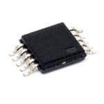
| 供应商器件封装 | 10-MSOP |
| 信噪比 | 92.7 dB |
| 分辨率 | 16 bit |
| 包装 | 管件 |
| 商标 | Analog Devices |
| 安装类型 | 表面贴装 |
| 安装风格 | SMD/SMT |
| 封装 | Tube |
| 封装/外壳 | 10-TFSOP,10-MSOP(0.118",3.00mm 宽) |
| 封装/箱体 | MSOP-10 |
| 工作温度 | -40°C ~ 85°C |
| 工作电源电压 | 5 V |
| 工厂包装数量 | 50 |
| 接口类型 | Serial (3-Wire, 4-Wire, SPI, QSPI, Microwire) |
| 数据接口 | DSP,MICROWIRE™,QSPI™,串行,SPI™ |
| 最大功率耗散 | 21.5 mW |
| 最大工作温度 | + 85 C |
| 最小工作温度 | - 40 C |
| 标准包装 | 1 |
| 电压参考 | External |
| 电压源 | 模拟和数字 |
| 系列 | AD7686 |
| 结构 | SAR |
| 转换器数 | 1 |
| 转换器数量 | 1 |
| 转换速率 | 500 kS/s |
| 输入数和类型 | 1 个伪差分,单极 |
| 输入类型 | Differential |
| 通道数量 | 1 Channel |
| 配用 | /product-detail/zh/EVAL-AD7686-PMDZ/EVAL-AD7686-PMDZ-ND/4875923/product-detail/zh/EVAL-AD7686CBZ/EVAL-AD7686CBZ-ND/1534679 |
| 采样率(每秒) | 500k |


PDF Datasheet 数据手册内容提取
16-Bit, 500 kSPS PulSAR ADC in MSOP Data Sheet AD7686 FEATURES FUNCTIONAL BLOCK DIAGRAM 16-bit resolution with no missing codes 0.5VTO 5V 5V Throughput: 500 kSPS INL: ±0.6 LSB typical, ±2 LSB maximum (±0.003% of FSR) SINAD: 92.5 dB at 20 kHz REF VDD VIO 1.8VTO VDD 0TO VREF THD: −110 dB at 20 kHz SDI IN+ Pseudo differential analog input range AD7686SCK 3- OR 4-WIRE INTERFACE IN– SDO (SPI, DAISY CHAIN, CS) 0 V to V with V up to VDD REF REF GND CNV No pipeline delay Sin1g.8le V-s/2u.p5p Vly/3 5 V V/ 5o Vpe loragtiico inn wteirtfha ce 02969-002 Figure 2. Proprietary serial interface: SPI-/QSPI™-/MICROWIRE™-/DSP- compatible Table 1. MSOP, LFCSP/SOT-23 14-/16-/18-Bit PulSAR ADC Daisy-chain multiple ADCs and busy indicator 400 kSPS Power dissipation 100 250 to 1000 ADC Type kSPS kSPS 500 kSPS kSPS Driver 3.75 µW at 5 V/100 SPS 18-Bit True AD7691 AD7690 AD7982 ADA4941 3.75 mW at 5 V/100 kSPS Differential AD7982 ADA4941 Standby current: 1 nA 16-Bit True AD7684 AD7687 AD7688 ADA4941 10-lead MSOP (MSOP-8 size) and Differential AD7693 ADA4841 3 mm × 3 mm, 10-lead LFCSP (SOT-23 size) 16-Bit Pseudo AD7680 AD7685 AD7686 AD7980 ADA4941 Pin-for-pin-compatible with 10-lead MSOP/PulSAR® ADCs Differential AD7683 AD7694 APPLICATIONS 14-Bit Pseudo AD7940 AD7942 AD7946 ADA4941 Differential Battery-powered equipment Data acquisitions GENERAL DESCRIPTION Instrumentation Medical instruments The AD76861 is a 16-bit, charge redistribution, successive Process controls approximation, analog-to-digital converter (ADC) that operates from a single 5 V power supply, VDD. It contains a low power, 2.0 high speed, 16-bit sampling ADC with no missing codes, an POSITIVE INL = +0.52LSB NEGATIVE INL =–0.38LSB internal conversion clock, and a versatile serial interface port. 1.5 The part also contains a low noise, wide bandwidth, short 1.0 aperture delay track-and-hold circuit. On the CNV rising edge, the AD7686 samples an analog input IN+ between 0 V to REF 0.5 B) with respect to a ground sense IN−. The reference voltage, REF, S L (L 0 is applied externally and can be set up to the supply voltage. IN Power dissipation scales linearly with throughput. –0.5 The SPI-compatible serial interface also features the ability, –1.0 using the SDI input, to daisy-chain several ADCs on a single, 3-wire bus or provides an optional busy indicator. This device is ––12..50 02969-007 csuopmpplya tVibIlOe .w ith 1.8 V, 2.5 V, 3 V, or 5 V logic, using the separate 0 16384 32768 49152 65535 CODE The AD7686 is housed in a 10-lead MSOP or a 10-lead LFCSP Figure 1. Integral Nonlinearity vs. Code with operation specified from −40°C to +85°C. 1. Protected by U.S. Patent 6,703,961. Rev. C Document Feedback Information furnished by Analog Devices is believed to be accurate and reliable. However, no responsibility is assumed by Analog Devices for its use, nor for any infringements of patents or other One Technology Way, P.O. Box 9106, Norwood, MA 02062-9106, U.S.A. rights of third parties that may result from its use. Specifications subject to change without notice. No license is granted by implication or otherwise under any patent or patent rights of Analog Devices. Tel: 781.329.4700 ©2005–2014 Analog Devices, Inc. All rights reserved. Trademarks and registered trademarks are the property of their respective owners. Technical Support www.analog.com
AD7686 Data Sheet TABLE OF CONTENTS Features .............................................................................................. 1 Driver Amplifier Choice ........................................................... 15 Applications ....................................................................................... 1 Voltage Reference Input ............................................................ 15 Functional Block Diagram .............................................................. 1 Power Supply ............................................................................... 15 General Description ......................................................................... 1 Supplying the ADC from the Reference .................................. 16 Revision History ............................................................................... 2 Digital Interface .......................................................................... 16 Specifications ..................................................................................... 3 CS MODE 3-Wire, No Busy Indicator .................................... 17 Timing Specifications ....................................................................... 5 CS Mode 3-Wire with Busy Indicator ..................................... 18 Absolute Maximum Ratings ............................................................ 6 CS Mode 4-Wire, No Busy Indicator ....................................... 19 ESD Caution .................................................................................. 6 CS Mode 4-Wire with Busy Indicator ..................................... 20 Pin Configurations and Function Descriptions ........................... 7 Chain Mode, No Busy Indicator .............................................. 21 Terminology ...................................................................................... 8 Chain Mode with Busy Indicator ............................................. 22 Typical Performance Characteristics ............................................. 9 Application Hints ........................................................................... 23 Theory of Operation ...................................................................... 12 Layout .......................................................................................... 23 Circuit Information .................................................................... 12 Evaluating the Performance of the AD7686 ............................ 23 Converter Operation .................................................................. 12 True 16-Bit Isolated Application Example .............................. 24 Typical Connection Diagram.................................................... 13 Outline Dimensions ....................................................................... 25 Analog Input ............................................................................... 14 Ordering Guide .......................................................................... 26 REVISION HISTORY 8/14—Rev. B to Rev. C 4/06—Rev. 0 to Rev. A Deleted QFN .................................................................. Throughout Updated Format .................................................................. Universal Change to Features Section ............................................................. 1 Updated Outline Dimensions ....................................................... 25 Added Patent Note, Note 1 .............................................................. 1 Changes to Ordering Guide .......................................................... 26 Added EPAD Notation to Figure 6 and Table 6............................ 7 Changes to Evaluating the Performance of the AD7686 4/05—Revision 0: Initial Version Section .............................................................................................. 23 Updated Outline Dimensions ....................................................... 25 Changes to Ordering Guide .......................................................... 26 3/07—Rev. A to Rev. B Changes to Features and Table 1..................................................... 1 Changes to Table 3 ............................................................................ 4 Moved Figure 3 and Figure 4 to Page ............................................. 5 Changes to Figure 13 and Figure 15 ............................................. 10 Changes to Figure 26 ...................................................................... 13 Changes to Table 8 .......................................................................... 15 Changes to Figure 31 ...................................................................... 16 Changes to Figure 42 ...................................................................... 21 Changes to Figure 44 ...................................................................... 22 Updated Outline Dimensions ....................................................... 25 Changes to Ordering Guide .......................................................... 26 Rev. C | Page 2 of 28
Data Sheet AD7686 SPECIFICATIONS VDD = 4.5 V to 5.5 V, VIO = 2.3 V to VDD, V = VDD, T = –40°C to +85°C, unless otherwise noted. REF A Table 2. B Grade C Grade Parameter Test Conditions/Comments Min Typ Max Min Typ Max Unit RESOLUTION 16 16 Bits ANALOG INPUT Voltage Range IN+ − IN− 0 V 0 V V REF REF Absolute Input Voltage IN+ −0.1 VDD + 0.1 −0.1 VDD + 0.1 V IN− −0.1 +0.1 −0.1 +0.1 V Analog Input CMRR f = 200 kHz 65 65 dB IN Leakage Current at 25° Acquisition phase 1 1 nA C Input Impedance See the Analog Input See the Analog Input section section ACCURACY No Missing Codes 16 16 Bits Differential Linearity Error −1 ±0.7 −1 ±0.5 +1.5 LSB1 Integral Linearity Error −3 ±1 +3 −2 ±0.6 +2 LSB1 Transition Noise REF = VDD = 5 V 0.5 0.45 LSB1 Gain Error2, T to T ±2 ±8 ±2 ±6 LSB1 MIN MAX Gain Error Temperature Drift ±0.3 ±0.3 ppm/°C Offset Error2, T to T ±0.1 ±1.6 ±0.1 ±1.6 mV MIN MAX Offset Temperature Drift ±0.3 ±0.3 ppm/°C Power Supply Sensitivity VDD = 5 V ± 5% ±0.05 ±0.05 LSB1 THROUGHPUT Conversion Rate 0 500 0 500 kSPS Transient Response Full-scale step 400 400 ns AC ACCURACY Signal-to-Noise Ratio f = 20 kHz, V = 5 V 89 92 91 92.7 dB3 IN REF f = 20 kHz, V = 2.5 V 87.5 88 dB2 IN REF Spurious-Free Dynamic Range f = 20 kHz −106 −110 dB2 IN Total Harmonic Distortion f = 20 kHz −106 −110 dB2 IN Signal-to-(Noise + Distortion) f = 20 kHz, V = 5 V 89 92 91 92.5 dB2 IN REF f = 20 kHz, V = 5 V, −60 dB input 32 33.5 dB2 IN REF Intermodulation Distortion4 −110 −115 dB2 1 LSB means least significant bit. With the 5 V input range, 1 LSB is 76.3 µV. 2 See the Terminology section. These specifications do include full temperature range variation, but do not include the error contribution from the external reference. 3 All specifications in dB are referred to a full-scale input FSR. Tested with an input signal at 0.5 dB below full scale, unless otherwise specified. 4 fIN1 = 21.4 kHz, fIN2 = 18.9 kHz, each tone at −7 dB below full scale. Rev. C | Page 3 of 28
AD7686 Data Sheet VDD = 4.5 V to 5.5 V, VIO = 2.3 V to VDD, V = VDD, T = –40°C to +85°C, unless otherwise noted. REF A Table 3. Parameter Test Conditions/Comments Min Typ Max Unit REFERENCE Voltage Range 0.5 VDD + 0.3 V Load Current 500 kSPS, REF = 5 V 100 µA SAMPLING DYNAMICS −3 dB Input Bandwidth 9 MHz Aperture Delay VDD = 5 V 2.5 ns DIGITAL INPUTS Logic Levels V –0.3 +0.3 × VIO V IL V 0.7 × VIO VIO + 0.3 V IH I −1 +1 µA IL I −1 +1 µA IH DIGITAL OUTPUTS Data Format Serial 16 bits straight binary Pipeline Delay Conversion results available immediately after completed conversion V I = +500 µA 0.4 V OL SINK V I = −500 µA VIO − 0.3 V OH SOURCE POWER SUPPLIES VDD Specified performance 4.5 5.5 V VIO Specified performance 2.3 VDD + 0.3 V VIO Range 1.8 VDD + 0.3 V Standby Current1, 2 VDD and VIO = 5 V, 25°C 1 50 nA Power Dissipation VDD = 5 V, 100 SPS throughput 3.75 µW VDD = 5 V, 100 kSPS throughput 3.75 4.3 mW VDD = 5 V, 500 kSPS throughput 15 21.5 mW TEMPERATURE RANGE3 Specified Performance T to T −40 +85 °C MIN MAX 1 With all digital inputs forced to VIO or GND as required. 2 During acquisition phase. 3 Contact sales for extended temperature range. Rev. C | Page 4 of 28
Data Sheet AD7686 TIMING SPECIFICATIONS −40°C to +85°C, VDD = 4.5 V to 5.5 V, VIO = 2.3 V to 5.5 V or VDD + 0.3 V, whichever is the lowest, unless otherwise stated. See Figure 3 and Figure 4 for load conditions. Table 4. Parameter Symbol Min Typ Max Unit Conversion Time: CNV Rising Edge to Data Available t 0.5 1.6 µs CONV Acquisition Time t 400 ns ACQ Time Between Conversions t 2 µs CYC CNV Pulse Width ( CS Mode) tCNVH 10 ns SCK Period (CS Mode) tSCK 15 ns SCK Period (Chain Mode) t SCK VIO Above 4.5 V 17 ns VIO Above 3 V 18 ns VIO Above 2.7 V 19 ns VIO Above 2.3 V 20 ns SCK Low Time t 7 ns SCKL SCK High Time t 7 ns SCKH SCK Falling Edge to Data Remains Valid t 5 ns HSDO SCK Falling Edge to Data Valid Delay t DSDO VIO Above 4.5 V 14 ns VIO Above 3 V 15 ns VIO Above 2.7 V 16 ns VIO Above 2.3 V 17 ns CNV or SDI Low to SDO D15 MSB Valid (CS Mode) tEN VIO Above 4.5 V 15 ns VIO Above 2.7 V 18 ns VIO Above 2.3 V 22 ns CNV or SDI High or Last SCK Falling Edge to SDO High Impedance (CS Mode) tDIS 25 ns SDI Valid Setup Time from CNV Rising Edge (CS Mode) tSSDICNV 15 ns SDI Valid Hold Time from CNV Rising Edge (CS Mode) tHSDICNV 0 ns SCK Valid Setup Time from CNV Rising Edge (Chain Mode) t 5 ns SSCKCNV SCK Valid Hold Time from CNV Rising Edge (Chain Mode) t 5 ns HSCKCNV SDI Valid Setup Time from SCK Falling Edge (Chain Mode) t 3 ns SSDISCK SDI Valid Hold Time from SCK Falling Edge (Chain Mode) t 4 ns HSDISCK SDI High to SDO High (Chain Mode with Busy Indicator) t DSDOSDI VIO Above 4.5 V 15 ns VIO Above 2.3 V 26 ns 70% VIO 500µA IOL 30% VIO tDELAY tDELAY TO SDO 1.4V 2V OR VIO – 0.5V1 2V OR VIO – 0.5V1 CL 0.8V OR 0.5V2 0.8V OR 0.5V2 50pF 12V IF VIO ABOVE 2.5V, VIO – 0.5V IF VIO BELOW 2.5V. 500µA IOH 02969-003 20.8V IF VIO ABOVE 2.5V, 0.5V IF VIO BELOW 2.5V. 02969-004 Figure 3. Load Circuit for Digital Interface Timing Figure 4. Voltage Levels for Timing Rev. C | Page 5 of 28
AD7686 Data Sheet ABSOLUTE MAXIMUM RATINGS Table 5. Stresses above those listed under Absolute Maximum Ratings Parameter Rating may cause permanent damage to the device. This is a stress Analog Inputs rating only; functional operation of the device at these or any IN+1, IN−1 GND − 0.3 V to VDD + 0.3 V other conditions above those indicated in the operational or ±130 mA section of this specification is not implied. Exposure to absolute REF GND − 0.3 V to VDD + 0.3 V maximum rating conditions for extended periods may affect Supply Voltages device reliability. VDD, VIO to GND −0.3 V to +7 V VDD to VIO ±7 V ESD CAUTION Digital Inputs to GND −0.3 V to VIO + 0.3 V Digital Outputs to GND −0.3 V to VIO + 0.3 V Storage Temperature Range −65°C to +150°C Junction Temperature 150°C θ Thermal Impedance 200°C/W (MSOP-10) JA θJC Thermal Impedance 44°C/W (MSOP-10) Lead Temperature JEDEC J-STD-20 1 See the Analog Input section. Rev. C | Page 6 of 28
Data Sheet AD7686 PIN CONFIGURATIONS AND FUNCTION DESCRIPTIONS REF 1 10 VIO VDD 2 AD7686 9 SDI IN+ 3 TOP VIEW 8 SCK (Not to Scale) REF 1 10 VIO IN– 4 7 SDO VDD 2 AD7686 9 SDI GND 5 6 CNV IN+ 3 TOP VIEW 8 SCK GINND– 45 (Not to Scale) 76 SCDNOV 02969-005 N1.O TMTEOEEX ESGPTOR EOSLEUEDNC DPT.AR TDIHC. IATSLH C EPO EENRXNFPEOOCRSTMEIODAN NP CIASED SN M.OUTS RTE BQEU ICROENDN TEOCTED02969-006 Figure 5. 10-Lead MSOP Pin Configuration Figure 6. 10-Lead LFCSP Pin Configuration Table 6. Pin Function Descriptions Pin No. Mnemonic Type1 Description 1 REF AI Reference Input Voltage. The REF range is from 0.5 V to VDD. It is referred to the GND pin. This pin should be decoupled closely to the pin with a 10 µF capacitor. 2 VDD P Power Supply. 3 IN+ AI Analog Input. It is referred to IN−. The voltage range, that is, the difference between IN+ and IN−, is 0 V to V . REF 4 IN− AI Analog Input Ground Sense. It is connected to the analog ground plane or to a remote sense ground. 5 GND P Power Supply Ground. 6 CNV DI Convert Input. This input has multiple functions. On its leading edge, it initiates the conversions and selects the interface mode, chain, or CS. In CS mode, it enables the SDO pin when low. In chain mode, the data should be read when CNV is high. 7 SDO DO Serial Data Output. The conversion result is output on this pin. It is synchronized to SCK. 8 SCK DI Serial Data Clock Input. When the part is selected, the conversion result is shifted out by this clock. 9 SDI DI Serial Data Input. This input provides multiple features. It selects the interface mode of the ADC as follows: Chain mode is selected if SDI is low during the CNV rising edge. In this mode, SDI is used as a data input to daisy-chain the conversion results of two or more ADCs onto a single SDO line. The digital data level on SDI is output on SDO with a delay of 16 SCK cycles. CS mode is selected if SDI is high during the CNV rising edge. In this mode, either SDI or CNV can enable the serial output signals when low. If SDI or CNV is low when the conversion is completed, the busy indicator feature is enabled. 10 VIO P Input/Output Interface Digital Power. Nominally at the same supply as the host interface (1.8 V, 2.5 V, 3 V, or 5 V). EPAD N/A Exposed Pad. The exposed pad must be connected to ground. This connection is not required to meet electrical performances. 1AI = analog input, DI = digital input, DO = digital output, and P = power. Rev. C | Page 7 of 28
AD7686 Data Sheet TERMINOLOGY Effective Number of Bits (ENOB) Integral Nonlinearity Error (INL) ENOB is a measurement of the resolution with a sine wave INL refers to the deviation of each individual code from a line input. It is related to SINAD by drawn from negative full scale through positive full scale. The point used as negative full scale occurs ½ LSB before the first ENOB = (SINAD − 1.76)/6.02 dB code transition. Positive full scale is defined as a level 1½ LSB and is expressed in bits. beyond the last code transition. The deviation is measured from Total Harmonic Distortion (THD) the middle of each code to the true straight line (see Figure 25). THD is the ratio of the rms sum of the first five harmonic Differential Nonlinearity Error (DNL) components to the rms value of a full-scale input signal and is In an ideal ADC, code transitions are 1 LSB apart. DNL is the expressed in dB. maximum deviation from this ideal value. It is often specified in Signal-to-Noise Ratio (SNR) terms of resolution for which no missing codes are guaranteed. SNR is the ratio of the rms value of the actual input signal to the Offset Error rms sum of all other spectral components below the Nyquist The first transition should occur at a level ½ LSB above analog frequency, excluding harmonics and dc. The value for SNR is ground (38.1 µV for the 0 V to 5 V range). The offset error is expressed in dB. the deviation of the actual transition from that point. Signal-to-(Noise + Distortion), SINAD Gain Error SINAD is the ratio of the rms value of the actual input signal to The last transition (from 111 . . . 10 to 111 . . . 11) should occur the rms sum of all other spectral components below the Nyquist for an analog voltage 1½ LSB below the nominal full scale frequency, including harmonics but excluding dc. The value for (4.999886 V for the 0 V to 5 V range). The gain error is the SINAD is expressed in dB. deviation of the actual level of the last transition from the ideal Aperture Delay level after the offset is adjusted out. It is the measure of the acquisition performance and is the time Spurious-Free Dynamic Range (SFDR) between the rising edge of the CNV input and when the input SFDR is the difference, in decibels (dB), between the rms signal is held for a conversion. amplitude of the input signal and the peak spurious signal. Transient Response Transient response is the time required for the ADC to accurately acquire its input after a full-scale step function is applied. Rev. C | Page 8 of 28
Data Sheet AD7686 TYPICAL PERFORMANCE CHARACTERISTICS 2.0 2.0 POSITIVE INL = +0.52LSB POSITIVE DNL = +0.35LSB NEGATIVE INL = –0.38LSB NEGATIVE DNL = –0.36LSB 1.5 1.5 1.0 1.0 0.5 0.5 NL (LSB) 0 NL (LSB) 0 I D –0.5 –0.5 –1.0 –1.0 ––12..50 02969-007 ––12..50 02969-010 0 16384 32768 49152 65535 0 16384 32768 49152 65535 CODE CODE Figure 7. Integral Nonlinearity vs. Code Figure 10. Differential Nonlinearity vs. Code 250000 160000 VDD = REF = 5V VDD = REF = 5V 140000 133575 202719 200000 124164 120000 100000 150000 S S NT NT 80000 U U O O C100000 C 60000 40000 50000 27583 30770 0 0 0 26 22 0 0 02969-008 200000 0 0 1703 1678 0 0 02969-011 8026 8027 8028 8029 802A 802B 802C 802D 802E 8024 8025 8026 8027 8028 8029 802A 802B CODE IN HEX CODE IN HEX Figure 8. Histogram of a DC Input at the Code Center Figure 11. Histogram of a DC Input at the Code Transition 0 95 –105 8192 POINT FFT VDD = REF = 5V –20 fS = 500kSPS LE) –40 fSINN R= 1=9 9.929.8kdHBz 94 –108 CA THD = –108.7dB THD S –60 SECOND HARMONIC = –110.1dB ULL THIRD HARMONIC = –119.2dB 93 –111 E (dB OF F–1–0800 SNR (dB) 92 SNR –114 THD (dB) D–120 U T MPLI–140 91 –117 A ––116800 02969-009 90 –120 02969-012 0 20 40 60 80 100 120 140 160 180 200 220 240 –10 –8 –6 –4 –2 0 FREQUENCY (kHz) INPUT LEVEL (dB) Figure 9. FFT Plot Figure 12. SNR and THD vs. Input Level Rev. C | Page 9 of 28
AD7686 Data Sheet 100 17.0 –90 –95 95 16.0 –100 SNR THD NR, SINAD (dB) 90 ENOB SINAD 15.0 ENOB (Bits) HD, SFDR (dB)–––111011505 SFDR S T 85 14.0 –120 70 13.0 02969-013 ––112350 02969-016 2.3 2.7 3.1 3.5 3.9 4.3 4.7 5.1 5.5 2.3 2.7 3.1 3.5 3.9 4.3 4.7 5.1 5.5 REFERENCE VOLTAGE (V) REFERENCE VOLTAGE (V) Figure 13. SNR, SINAD, and ENOB vs. Reference Voltage Figure 16. THD, SFDR vs. Reference Voltage 100 –90 VREF = 5V VREF = 5V 95 –100 B) B) R (d 90 D (d –110 N H S T 85 –120 80 02969-014 –130 02969-017 –55 –35 –15 5 25 45 65 85 105 125 –55 –35 –15 5 25 45 65 85 105 125 TEMPERATURE (°C) TEMPERATURE (°C) Figure 14. SNR vs. Temperature Figure 17. THD vs. Temperature 100 –60 95 –70 VREF = 5V, –10dB 90 –80 dB) B) VREF = 5V, –1dB AD ( 85 VREF = 5V, –1dB D (d –90 N H SI T 80 –100 75 –110 VREF = 5V, –10dB 70 02969-015 –120 02969-018 0 50 100 150 200 0 50 100 150 200 FREQUENCY (kHz) FREQUENCY (kHz) Figure 15. SINAD vs. Frequency Figure 18. THD vs. Frequency Rev. C | Page 10 of 28
Data Sheet AD7686 1000 4 fS = 100kSPS 3 VDD µA) 750 B) 2 S ( LS NT R ( 1 OFFSET ERROR E O ATING CURR 500 T, GAIN ERR ––01 GAIN ERROR R E E S OP 250 FF –2 O 0 VIO 02969-019 ––34 02969-022 4.50 4.75 5.00 5.25 5.50 –55 –35 –15 5 25 45 65 85 105 125 SUPPLY (V) TEMPERATURE (°C) Figure 19. Operating Currents vs. Supply Figure 22. Offset and Gain Error vs. Temperature 1000 25 S (nA) 750 20 T N URRE Y (ns) 15 WN C 500 DELA VDD = 5V, 85°C DO DO 10 ER- TDS VDD = 5V, 25°C W 250 O P 5 0–55 –35 –15 5 25 45 65 VDD8 +5 VIO 105 12502969-020 0 02969-023 0 20 40 60 80 100 120 TEMPERATURE (°C) SDO CAPACITIVE LOAD (pF) Figure 20. Power-Down Currents vs. Temperature Figure 23. t Delay vs. Capacitance Load and Supply DSDO 1000 fS = 100kSPS VDD = 5V µA) 750 S ( T N E R R CU 500 G N TI A R E P 250 O 0 VIO 02969-021 –55 –35 –15 5 25 45 65 85 105 125 TEMPERATURE (°C) Figure 21. Operating Currents vs. Temperature Rev. C | Page 11 of 28
AD7686 Data Sheet THEORY OF OPERATION IN+ SWITCHES CONTROL MSB LSB SW+ 32,768C 16,384C 4C 2C C C BUSY REF CONTROL COMP LOGIC GND OUTPUT CODE 32,768C 16,384C 4C 2C C C MSB LSB SW– CNV IN– 02969-024 Figure 24. ADC Simplified Schematic CIRCUIT INFORMATION CONVERTER OPERATION The AD7686 is a fast, low power, single-supply, precise 16-bit The AD7686 is a successive approximation ADC based on a ADC using a successive approximation architecture. charge redistribution DAC. Figure 24 shows a simplified schematic of the ADC. The capacitive DAC consists of two The AD7686 is capable of converting 500,000 samples per identical arrays of 16 binary weighted capacitors, which are second (500 kSPS) and powers down between conversions. connected to two comparator inputs. For example, when operating at 100 SPS, the device consumes 3.75 µW typically, which is ideal for battery-powered During the acquisition phase, terminals of the array tied to the applications. comparator input are connected to GND via SW+ and SW−. All independent switches are connected to the analog inputs. The AD7686 provides the user with on-chip, track-and-hold Therefore, the capacitor arrays are used as sampling capacitors and does not exhibit any pipeline delay or latency, making it and acquire the analog signal on the IN+ and IN− inputs. When ideal for multiple, multiplexed channel applications. the acquisition phase is complete and the CNV input goes high, The AD7686 is specified from 4.5 V to 5.5 V and can be a conversion phase initiates. When the conversion phase begins, interfaced to any of the 1.8 V to 5 V digital logic family. It is SW+ and SW− are opened first. housed in a 10-lead MSOP or a tiny 10-lead LFCSP that The two capacitor arrays are then disconnected from the inputs combines space savings and allows flexible configurations. and connected to the GND input. Therefore, the differential This device is pin-for-pin-compatible with the AD7685, voltage between the inputs IN+ and IN−, captured at the end of AD7687, and AD7688. the acquisition phase, is applied to the comparator inputs, causing the comparator to become unbalanced. By switching each element of the capacitor array between GND and REF, the comparator input varies by binary weighted voltage steps (V /2, V /4 . . . V /65536). The control logic REF REF REF toggles these switches, starting with the MSB, to bring the comparator back into a balanced condition. After the completion of this process, the part returns to the acquisition phase and the control logic generates the ADC output code and a busy signal indicator. Because the AD7686 has an on-board conversion clock, the serial clock, SCK, is not required for the conversion process. Rev. C | Page 12 of 28
Data Sheet AD7686 Transfer Functions Table 7. Output Codes and Ideal Input Voltages The ideal transfer characteristic for the AD7686 is shown in Analog Input Digital Output Code Figure 25 and Table 7. Description VREF = 5 V Hexadecimal FSR – 1 LSB 4.999924 V FFFF1 Midscale + 1 LSB 2.500076 V 8001 Y) Midscale 2.5 V 8000 AR 111...111 Midscale – 1 LSB 2.499924 V 7FFF T BIN 111111......111001 –FSR + 1 LSB 76.3 µV 0001 H G –FSR 0 V 00002 AI R ST E ( OD TYPICAL CONNECTION DIAGRAM C C D Figure 26 shows an example of the recommended connection A 000...010 diagram for the AD7686 when multiple supplies are available. 000...001 000...000 –FSR –FSR + 1 LSB +FSR – 1 LSB 1 This is also the code for an overranged analog input (VIN+ − VIN− above VREF − VGND). –FSR + 0.5 LSB ANALOG+ IFNSPRU T– 1.5 LSB 02969-025 2 This is also the code for an underranged analog input (VIN+ − VIN− below VGND). Figure 25. ADC Ideal Transfer Function ≥7V REF1 5V 10µF2 100nF 1.8VTO VDD ≥7V 100nF REF VDD VIO 33Ω IN+ SDI 0TO VREF SCK 3 2.7nF AD7686 3- OR 4-WIRE INTERFACE5 ≤–2V SDO 4 IN– CNV GND 1SEE THE VOLTAGE REFERENCE INPUT SECTION FOR REFERENCE SELECTION. 2CREF IS USUALLY A 10µF CERAMIC CAPACITOR (X5R). 345SOSEEPEET IDDORINGIAVITLEA RFLI ALINTMETPERLR.I FSFAIEECEREA C NSHEAOCLIOTCIGEO NSINE FPCOUTRTIO MSNEO.CSTTI OCNO.NVENIENT INTERFACE MODE. 02969-026 Figure 26. Typical Application Diagram with Multiple Supplies Rev. C | Page 13 of 28
AD7686 Data Sheet ANALOG INPUT During the acquisition phase, the impedance of the analog inputs (IN+ or IN−) can be modeled as a parallel combination Figure 27 shows an equivalent circuit of the input structure of capacitor, C , and the network formed by the series of the AD7686. The two diodes, D1 and D2, provide ESD PIN connection of R and C . C is primarily the pin capacitance. protection for the analog inputs IN+ and IN−. Care must be IN IN PIN R is typically 600 Ω and is a lumped component made up of taken to ensure that the analog input signal never exceeds the IN some serial resistors and the on resistance of the switches. C is supply rails by more than 0.3 V because this causes these IN typically 30 pF and is mainly the ADC sampling capacitor. diodes to begin to forward-bias and start conducting current. During the conversion phase, where the switches are opened, These diodes can handle a forward-biased current of 130 mA the input impedance is limited to C . R and C make a maximum. For instance, these conditions could eventually PIN IN IN 1-pole, low-pass filter that reduces undesirable aliasing effects occur when the input buffer’s (U1) supplies are different from and limits the noise. VDD. In such a case, an input buffer with a short-circuit current limitation can be used to protect the part. When the source impedance of the driving circuit is low, the AD7686 can be driven directly. Large source impedances VDD significantly affect the ac performance, especially THD. The dc IN+ D1 RIN CIN performances are less sensitive to the input impedance. The OR IN– maximum source impedance depends on the amount of THD CPIN D2 GND 02969-027 tshoautr ccea nim bpe etdolaenrcaete adn. dT thhee T mHaDxi mdeugmra dineps uats far efuqunecnticoyn, aosf sthheo wn in Figure 29. Figure 27. Equivalent Analog Input Circuit –80 The analog input structure allows the sampling of the differential signal between IN+ and IN−. By using this –85 differential input, small signals common to both inputs are rejected, as shown in Figure 28, which represents the typical –90 CMRR over frequency. For instance, by using IN− to sense a remote signal ground, ground potential differences between B) the sensor and the local ADC ground are eliminated. D (d –95 TH RS = 250Ω 80 –100 –105 RS = 100Ω 70 VDD = 5V –110 RRSS == 3530ΩΩ 02969-030 0 25 50 75 100 dB) FREQUENCY (kHz) R ( 60 Figure 29. THD vs. Analog Input Frequency and Source Resistance R M C 50 40 02969-028 1 10 100 1000 10000 FREQUENCY (kHz) Figure 28. Analog Input CMRR vs. Frequency Rev. C | Page 14 of 28
Data Sheet AD7686 DRIVER AMPLIFIER CHOICE VOLTAGE REFERENCE INPUT Although the AD7686 is easy to drive, the driver amplifier The AD7686 voltage reference input, REF, has a dynamic input should meet the following requirements: impedance and should, therefore, be driven by a low impedance source with efficient decoupling between the REF and GND • The noise generated by the driver amplifier needs to be pins, as explained in the Layout section. kept as low as possible to preserve the SNR and transition noise performance of the AD7686. Note that the AD7686 When REF is driven by a very low impedance source, such as a has a noise much lower than most of the other 16-bit reference buffer using the AD8031 or the AD8605, a 10 µF ADCs and, therefore, can be driven by a noisier amplifier (X5R, 0805 size) ceramic chip capacitor is appropriate for to meet a given system noise specification. The noise optimum performance. coming from the amplifier is filtered by the AD7686 analog If an unbuffered reference voltage is used, the decoupling value input circuit 1-pole, low-pass filter made by R and C or IN IN depends on the reference used. For instance, a 22 µF (X5R, by the external filter, if one is used. Because the typical 1206 size) ceramic chip capacitor is appropriate for optimum noise of the AD7686 is 37 µV rms, the SNR degradation performance using a low temperature drift ADR43x reference. due to the amplifier is If desired, smaller reference decoupling capacitor values down to 2.2 µF can be used with a minimal impact on performance, 37 especially DNL. SNR =20log LOSS 372+π f (Ne )2 Regardless, there is no need for an additional lower value 2 −3dB N ceramic decoupling capacitor, such as 100 nF, between the REF and GND pins. where: POWER SUPPLY f is the input bandwidth in MHz of the AD7686 –3dB (9 MHz) or the cutoff frequency of the input filter, if The AD7686 is specified at 4.5 V to 5.5 V. The device uses two one is used. power supply pins: a core supply VDD and a digital input/ N is the noise gain of the amplifier (for example, 1 in buffer output interface supply VIO. VIO allows direct interface with configuration). any logic between 1.8 V and VDD. To reduce the supplies needed, the VIO and VDD can be tied together. e is the equivalent input noise voltage of the op amp, N in nV/√Hz. The AD7686 is independent of power supply sequencing between VIO and VDD. Additionally, it is very insensitive to • For ac applications, the driver should have a THD power supply variations over a wide frequency range, as shown performance commensurate with the AD7686. Figure 18 in Figure 30, which represents PSRR over frequency. shows the THD vs. frequency that the driver should exceed. 110 • For multichannel multiplexed applications, the driver 100 amplifier and the AD7686 analog input circuit must settle a full-scale step onto the capacitor array at a 16-bit level 90 (0.0015%). In the data sheet for the amplifier, settling at 0.1% to 0.01% is more commonly specified. This could 80 VDD = 5V B) differ significantly from the settling time at a 16-bit level R (d 70 R and should be verified prior to driver selection. S P 60 Table 8. Recommended Driver Amplifiers 50 Amplifier Typical Application AADDA8640854,1 A-xD 8615 V5 eVr ysi lnogwle n-souispep alyn, dlo lwow p opwowere r 4300 02969-031 1 10 100 1000 10000 AD8655 5 V single-supply, low power FREQUENCY (kHz) OP184 Low power, low noise, and low frequency Figure 30. PSRR vs. Frequency AD8021 Very low noise and high frequency AD8022 Very low noise and high frequency AD8519 Small, low power and low frequency AD8031 High frequency and low power Rev. C | Page 15 of 28
AD7686 Data Sheet The AD7686 powers down automatically at the end of each DIGITAL INTERFACE conversion phase and, therefore, the power scales linearly with Though the AD7686 has a reduced number of pins, it offers the sampling rate, as shown in Figure 31. This makes the part flexibility in its serial interface modes. ideal for low sampling rates (even a few Hz) and low battery- powered applications. The AD7686, when in CS mode, is compatible with SPI, QSPI, digital hosts, and DSPs, such as Blackfin® ADSP-BF53x or 10000 ADSP-219x. This interface can use either 3-wire or 4-wire. A 1000 3-wire interface using the CNV, SCK, and SDO signals VDD = 5V A) minimizes wiring connections useful, for instance, in isolated µ S ( 100 applications. A 4-wire interface using the SDI, CNV, SCK, and T EN SDO signals allows CNV, which initiates the conversions, to be R 10 UR VIO independent of the readback timing (SDI). This is useful in low C NG 1 jitter sampling or simultaneous sampling applications. TI RA The AD7686, when in chain mode, provides a daisy-chain E 0.1 OP feature using the SDI input for cascading multiple ADCs on a 0.01 single data line similar to a shift register. The mode in which the part operates depends on the SDI level 0.00110 100 SAM10P0L0ING RAT1E00 (0S0PS) 100000 1000000 02969-032 wSDhIe nis thhieg hC,N anVd r tishien gch eadigne m ooccduer iss. sTehleec CteSd m if oSdDeI i iss s leolwec. tTedh ei f Figure 31. Operating Currents vs. Sampling Rate SDI hold time is such that when SDI and CNV are connected SUPPLYING THE ADC FROM THE REFERENCE together, the chain mode is always selected. For simplified applications, the AD7686, with its low operating In either mode, the AD7686 offers the flexibility to optionally current, can be supplied directly using the reference circuit force a start bit in front of the data bits. This start bit can be shown in Figure 32. The reference line can be driven by either: used as a busy signal indicator to interrupt the digital host and trigger the data reading. Otherwise, without a busy indicator, • The system power supply directly. the user must timeout the maximum conversion time prior to • A reference voltage with enough current output capability, readback. such as the ADR43x. The busy indicator feature is enabled as follows: • A reference buffer, such as the AD8031, which can also • In CS mode, if CNV or SDI is low when the ADC conversion filter the system power supply, as shown in Figure 32. ends (see Figure 36 and Figure 40). 5V • In chain mode, if SCK is high during the CNV rising edge 5V 10Ω (see Figure 44). 5V 10kΩ AD8031 10µF 1µF 1µF 1 REF VDD VIO AD7686 1OPTIONAL REFERENCE BUFFERAND FILTER. 02969-033 Figure 32. Example of Application Circuit Rev. C | Page 16 of 28
Data Sheet AD7686 CS MODE 3-WIRE, NO BUSY INDICATOR The data is valid on both SCK edges. Although the rising edge can be used to capture the data, a digital host using the SCK This mode is most often used when a single AD7686 is falling edge allows a faster reading rate provided it has an connected to an SPI-compatible digital host. The connection acceptable hold time. After the 16th SCK falling edge, or when diagram is shown in Figure 33, and the corresponding timing is CNV goes high, whichever occurs first, SDO returns to high provided in Figure 34. impedance. With SDI tied to VIO, a rising edge on CNV initiates a conversion, selects the CS mode, and forces SDO to high CONVERT impedance. Once a conversion is initiated, it continues to completion irrespective of the state of CNV. For instance, it CNV DIGITAL HOST VIO could be useful to bring CNV low to select other SPI devices, SDI AD7686 SDO DATA IN such as analog multiplexers. However, CNV must be returned SCK high before the minimum conversion time and held high until tshigen mala ixnidmicuamto rc.o Wnvheernsi othne t cimonev teor saivooni dis g ceonmerpalteitneg, tthhee AbuDs7y6 86 CLK 02969-034 enters the acquisition phase and powers down. When CNV Figure 33. CS Mode 3-Wire, No Busy Indicator goes low, the MSB is output onto SDO. The remaining data bits Connection Diagram (SDI High) are then clocked by subsequent SCK falling edges. SDI = 1 tCYC tCNVH CNV tCONV tACQ ACQUISITION CONVERSION ACQUISITION tSCK tSCKL SCK 1 2 3 14 15 16 tHSDO tSCKH tEN tDSDO tDIS SDO D15 D14 D13 D1 D0 02969-035 Figure 34. CS Mode 3-Wire, No Busy Indicator Serial Interface Timing (SDI High) Rev. C | Page 17 of 28
AD7686 Data Sheet CS MODE 3-WIRE WITH BUSY INDICATOR Although the rising edge can be used to capture the data, a digital host using the SCK falling edge allows a faster reading This mode is generally used when a single AD7686 is connected rate, provided it has an acceptable hold time. After the optional to an SPI-compatible digital host having an interrupt input. The 17th SCK falling edge or when CNV goes high, whichever connection diagram is shown in Figure 35, and the correspond- occurs first, SDO returns to high impedance. ing timing is provided in Figure 36. If multiple AD7686s are selected at the same time, the SDO With SDI tied to VIO, a rising edge on CNV initiates a output pin handles this connection without damage or induced conversion, selects the CS mode, and forces SDO to high latch-up. Meanwhile, it is recommended to keep this connection as impedance. SDO is maintained in high impedance until the short as possible to limit extra power dissipation. completion of the conversion, irrespective of the state of CNV. Prior to the minimum conversion time, CNV can be used to CONVERT select other SPI devices, such as analog multiplexers. However, VIO CNV must be returned low before the minimum conversion CNV DIGITAL HOST time and held low until the maximum conversion time to VIO 47kΩ SDI AD7686 SDO DATA IN guarantee the generation of the busy signal indicator. When the conversion is complete, SDO goes from high impedance to low. SCK IRQ With a pull-up on the SDO line, this transition can be used as adnig iintatle rhrouspt.t Tsihgen aAl Dto7 6in8i6ti tahtee nth een dteartsa trheea daicnqgu icsoitnitorno lplehda sbey a tnhde CLK 02969-036 Figure 35. CS Mode 3-Wire with Busy Indicator powers down. The data bits are then clocked out, MSB first, by Connection Diagram (SDI High) subsequent SCK falling edges. The data is valid on both SCK edges. SDI = 1 tCYC tCNVH CNV tCONV tACQ ACQUISITION CONVERSION ACQUISITION tSCK tSCKL SCK 1 2 3 15 16 17 tHSDO tSCKH tDSDO tDIS SDO D15 D14 D1 D0 02969-037 Figure 36. CS Mode 3-Wire with Busy Indicator Serial Interface Timing (SDI High) Rev. C | Page 18 of 28
Data Sheet AD7686 CS MODE 4-WIRE, NO BUSY INDICATOR avoid the generation of the busy signal indicator. When the conversion is complete, the AD7686 enters the acquisition This mode is generally used when multiple AD7686s are phase and powers down. Each ADC result can be read by connected to an SPI-compatible digital host. A connection bringing its SDI input low, which consequently outputs the MSB diagram example using two AD7686 devices is shown in onto SDO. The remaining data bits are then clocked by Figure 37, and the corresponding timing is given in Figure 38. subsequent SCK falling edges. The data is valid on both SCK With SDI high, a rising edge on CNV initiates a conversion, edges. Although the rising edge can be used to capture the data, selects the CS mode, and forces SDO to high impedance. In this a digital host using the SCK falling edge allows a faster reading mode, CNV must be held high during the conversion phase and rate, provided it has an acceptable hold time. After the 16th the subsequent data readback (if SDI and CNV are low, SDO is SCK falling edge or when SDI goes high, whichever occurs first, driven low). Prior to the minimum conversion time, SDI could SDO returns to high impedance and another AD7686 can be used to select other SPI devices, such as analog multiplexers. be read. but SDI must be returned high before the minimum conversion time and held high until the maximum conversion time to CS2 CS1 CONVERT DIGITAL HOST CNV CNV SDI AD7686 SDO SDI AD7686 SDO SCK SCK DCLAKTA IN 02969-038 Figure 37. CS Mode 4-Wire, No Busy Indicator Connection Diagram tCYC CNV tCONV tACQ ACQUISITION CONVERSION ACQUISITION tSSDICNV SDI(CS1) tHSDICNV SDI(CS2) tSCK tSCKL SCK 1 2 3 14 15 16 17 18 30 31 32 tHSDO tSCKH tEN tDSDO tDIS SDO D15 D14 D13 D1 D0 D15 D14 D1 D0 02969-039 Figure 38. CS Mode 4-Wire, No Busy Indicator Serial Interface Timing Rev. C | Page 19 of 28
AD7686 Data Sheet CS MODE 4-WIRE WITH BUSY INDICATOR With a pull-up on the SDO line, this transition can be used as an interrupt signal to initiate the data readback controlled by This mode is usually used when a single AD7686 is connected the digital host. The AD7686 then enters the acquisition phase to an SPI-compatible digital host, which has an interrupt input, and powers down. The data bits are then clocked out, MSB first, and when it is desired to keep CNV, which is used to sample the by subsequent SCK falling edges. The data is valid on both SCK analog input, independent of the signal used to select the data edges. Although the rising edge can be used to capture the data, reading. This requirement is particularly important in applications a digital host using the SCK falling edge allows a faster reading where low jitter on CNV is desired. The connection diagram is rate, provided it has an acceptable hold time. After the optional shown in Figure 39, and the corresponding timing is provided 17th SCK falling edge or SDI going high, whichever occurs first, in Figure 40. the SDO returns to high impedance. With SDI high, a rising edge on CNV initiates a conversion, selects the CS mode, and forces SDO to high impedance. In this CS1 CONVERT mode, CNV must be held high during the conversion phase and VIO the subsequent data readback (if SDI and CNV are low, SDO is CNV DIGITAL HOST driven low). Prior to the minimum conversion time, SDI can be 47kΩ SDI AD7686 SDO DATA IN used to select other SPI devices, such as analog multiplexers, but SDI must be returned low before the minimum conversion SCK IRQ time and held low until the maximum conversion time to gcounarvaenrsteioen t hise cgoemneprlaettieo, nS DofO th geo beus sfyro smig nhaigl hin idmicpaetodra.n Wceh teon l ow. CLK 02969-040 Figure 39. CS Mode 4-Wire with Busy Indicator Connection Diagram tCYC CNV tCONV tACQ ACQUISITION CONVERSION ACQUISITION tSSDICNV SDI tHSDICNV tSCK tSCKL SCK 1 2 3 15 16 17 tHSDO tSCKH tDSDO tDIS SDO tEN D15 D14 D1 D0 02969-041 Figure 40. CS Mode 4-Wire with Busy Indicator Serial Interface Timing Rev. C | Page 20 of 28
Data Sheet AD7686 CHAIN MODE, NO BUSY INDICATOR When the conversion is complete, the MSB is output onto SDO, and the AD7686 enters the acquisition phase and powers down. This mode can be used to daisy-chain multiple AD7686s on a The remaining data bits stored in the internal shift register are 3-wire serial interface. This feature is useful for reducing then clocked by subsequent SCK falling edges. For each ADC, component count and wiring connections, for example, in SDI feeds the input of the internal shift register and is clocked isolated multiconverter applications or for systems with a by the SCK falling edge. Each ADC in the chain outputs its data limited interfacing capacity. Data readback is analogous to MSB first, and 16 × N clocks are required to read back the N clocking a shift register. ADCs. The data is valid on both SCK edges. Although the rising A connection diagram example using two AD7686s is shown in edge can be used to capture the data, a digital host using the Figure 41, and the corresponding timing is given in Figure 42. SCK falling edge allows a faster reading rate and, consequently, When SDI and CNV are low, SDO is driven low. With SCK low, more AD7686s in the chain, provided the digital host has an a rising edge on CNV initiates a conversion, selects the chain acceptable hold time. The maximum conversion rate can be mode, and disables the busy indicator. In this mode, CNV is reduced due to the total readback time. For instance, with a 3 ns held high during the conversion phase and the subsequent data digital host setup time and 3 V interface, up to four AD7686s readback. running at a conversion rate of 360 kSPS can be daisy-chained on a 3-wire port. CONVERT CNV CNV DIGITAL HOST SDI AD7686 SDO SDI AD7686 SDO DATA IN A B SCK SCK CLK 02969-042 Figure 41. Chain Mode, No Busy Indicator Connection Diagram SDIA = 0 tCYC CNV tCONV tACQ ACQUISITION CONVERSION ACQUISITION tSCK tSSCKCNV tSCKL SCK 1 2 3 14 15 16 17 18 30 31 32 tHSCKCNV tSSDISCK tSCKH tEN tHSDISCK SDOA = SDIB DA15 DA14 DA13 DA1 DA0 tHSDO tDSDO SDOB DB15 DB14 DB13 DB1 DB0 DA15 DA14 DA1 DA0 02969-043 Figure 42. Chain Mode, No Busy Indicator Serial Interface Timing Rev. C | Page 21 of 28
AD7686 Data Sheet CHAIN MODE WITH BUSY INDICATOR This transition on SDO can be used as a busy indicator to trigger the data readback controlled by the digital host. The This mode can be used to daisy-chain multiple AD7686s AD7686 then enters the acquisition phase and powers down. on a 3-wire serial interface while providing a busy indicator. The data bits stored in the internal shift register are then This feature is useful for reducing component count and clocked out, MSB first, by subsequent SCK falling edges. For wiring connections, for example, in isolated multiconverter each ADC, SDI feeds the input of the internal shift register and applications or for systems with a limited interfacing capacity. is clocked by the SCK falling edge. Each ADC in the chain Data readback is analogous to clocking a shift register. A outputs its data MSB first, and 16 × N + 1 clocks are required to connection diagram example using three AD7686s is shown in readback the N ADCs. Figure 43, and the corresponding timing is given in Figure 44. Although the rising edge can be used to capture the data, a When SDI and CNV are low, SDO is driven low. With SCK digital host using the SCK falling edge allows a faster reading high, a rising edge on CNV initiates a conversion, selects the rate and, consequently, more AD7686s in the chain, provided chain mode, and enables the busy indicator feature. In this the digital host has an acceptable hold time. For instance, mode, CNV is held high during the conversion phase and the with a 3 ns digital host setup time and 3 V interface, up to four subsequent data readback. When all ADCs in the chain have AD7686s running at a conversion rate of 360 kSPS can be daisy completed their conversions, the near-end ADC (ADC C in chained to a single 3-wire port. Figure 43) SDO is driven high. CONVERT CNV CNV CNV DIGITAL HOST SDI AD7686 SDO SDI AD7686 SDO SDI AD7686 SDO DATA IN A B C SCK SCK SCK IRQ CLK 02969-044 Figure 43. Chain Mode with Busy Indicator Connection Diagram tCYC CNV = SDIA tCONV tACQ ACQUISITION CONVERSION ACQUISITION tSSCKCNV tSCKH tSCK SCK 1 2 3 4 15 16 17 18 19 31 32 33 34 35 47 48 49 tHSCKCNV tEN tSSDISCK tHSDISCK tSCKL tDSDOSDI SDOA = SDIB DA15 DA14 DA13 DA1 DA0 ttHDSSDDOO tDSDOSDI SDOB = SDIC tDSDOSDI DB15 DB14 DB13 DB1 DB0 DA15 DA14 DA1 DA0 tDSDOSDI tDSDOSDI SDOC DC15 DC14 DC13 DC1 DC0 DB15 DB14 DB1 DB0 DA15 DA14 DA1 DA0 02969-045 Figure 44. Chain Mode with Busy Indicator Serial Interface Timing Rev. C | Page 22 of 28
Data Sheet AD7686 APPLICATION HINTS LAYOUT The printed circuit board (PCB) that houses the AD7686 should be designed so that the analog and digital sections are separated and confined to certain areas of the board. The pinout of the AD7686, with all its analog signals on the left side and all its digital signals on the right side, eases this task. Avoid running digital lines under the device because doing so couples noise onto the die, unless a ground plane under the AD7686 is used as a shield. Fast switching signals, such as CNV or clocks, should never run near analog signal paths. Crossover of digital and analog signals should be avoided. At least one ground plane should be used. It could be common ocars sep, ltiht eb eptlwaneeesn sthhoeu dldig bitea lj oainnde dan uanlodge rsneecatitohn tsh. eI nd ethviec least.t er 02969-046 Figure 45. Example of Layout of the AD7686 (Top Layer) The AD7686 voltage reference input REF has a dynamic input impedance and should be decoupled with minimal parasitic inductances. This is done by placing the reference decoupling ceramic capacitor close to, and ideally right up against, the REF and GND pins and connecting it with wide, low impedance traces. Finally, the AD7686 power supplies VDD and VIO should be decoupled with ceramic capacitors (typically 100 nF) placed close to the AD7686 and connected using short and wide traces. This provides low impedance paths and reduces the effect of glitches on the power supply lines. Examples of layouts that follow these rules are shown in Figure 45 and Figure 46. EVALUATING THE PERFORMANCE OF THE AD7686 Other recommended layouts for the AD7686 are outlined in 02969-047 the documentation of the EVAL-AD7686SBZ evaluation board. Figure 46. Example of Layout of the AD7686 (Bottom Layer) The EVAL-AD7686SBZ evaluation board package includes a fully assembled and tested evaluation board, documentation, and software for controlling the board from a PC via the EVAL- SDP-CB1Z. Rev. C | Page 23 of 28
AD7686 Data Sheet TRUE 16-BIT ISOLATED APPLICATION EXAMPLE This skew is the channel-to-channel matching propagation delay of the digital isolator (t ). This allows running the In applications where high accuracy and isolation are required, PSKCD serial interface at the maximum speed of the digital isolator such as power monitoring, motor control, and some medical (45 Mbps for the ADuM1402C), which would have been equipment, the circuit shown in Figure 47, using the AD7686 otherwise limited by the cascade of the propagation delays of and the ADuM1402C digital isolator, provides a compact and the digital isolator. For instance, four AD7686 devices running high performance solution. at 330 kSPS can be chained together. Multiple AD7686 devices are daisy-chained to reduce the The complete analog chain runs on a single 5 V supply using number of signals to isolate. Note that the SCKOUT, which is a the ADR391 low dropout reference voltage and the rail-to-rail readback of the AD7686 clock, has a very short skew with the CMOS AD8618 amplifier while offering true bipolar input range. DATA signal. 5V VDD1, VE1 VDD2, VE2 2.7VTO 5V 100nF 100nF 5V REF 5V GND1 GND2 10µF 100nF VIA VOA DATA 4kΩ 1kΩ ±10V INPUT 5V REFVDD VIO SDO VIB VOB SCKOUT SCK IN+ AD7686 2V REF CNV VOC VIC SCKIN IN– GND SDI 1/4AD8618 VOD VID CONVERT 5V REF 5V 10µF 100nF ADuM1402C 4kΩ 1kΩ ±10V INPUT 5V REFVDD VIO SDO SCK IN+ AD7686 CNV 2V REF IN– GND SDI 1/4AD8618 5V REF 5V 10µF 100nF 4kΩ 1kΩ ±10V INPUT 5V REFVDD VIO SDO IN+ AD7686 SCK 1kΩ 1kΩ CNV 2V REF IN– GND SDI 5V 1/4AD8618 5V REF 5V REF 5V ADR391 10µF 100nF 1kΩ 5V IN OUT 2V REF 4kΩ 1kΩ ±10V INPUT GND 4kΩ 5V REFVDD VIO SDO IN+ AD7686 SCK 10µF 100nF CNV 2V REF 1/4AD8618 IN– GND SDI 02969-048 Figure 47. A True 16-Bit Isolated Simultaneous Sampling Acquisition System Rev. C | Page 24 of 28
Data Sheet AD7686 OUTLINE DIMENSIONS 3.10 3.00 2.90 10 6 5.15 3.10 4.90 3.00 4.65 2.90 1 5 PIN1 IDENTIFIER 0.50BSC 0.95 15°MAX 0.85 1.10MAX 0.75 0.70 0.15 0.30 6° 0.23 0.55 CO0P.0L5ANARITY 0.15 0° 0.13 0.40 0.10 COMPLIANTTOJEDECSTANDARDSMO-187-BA 091709-A Figure 48. 10-Lead Mini Small Outline Package [MSOP] (RM-10) Dimensions shown in millimeters 2.48 2.38 3.10 2.23 3.00 SQ 2.90 0.50 BSC 6 10 PIN 1 INDEX EXPOSED 1.74 AREA PAD 1.64 0.50 1.49 0.40 0.30 5 1 0.20 MIN TOP VIEW BOTTOM VIEW PIN 1 INDICATOR (R 0.15) 0.80 FOR PROPER CONNECTION OF 0.75 0.05 MAX THE EXPOSED PAD, REFER TO THE PIN CONFIGURATION AND 0.70 0.02 NOM FUNCTION DESCRIPTIONS COPLANARITY SECTION OF THIS DATA SHEET. SEPALTAINNGE 000...322050 0.20 REF 0.08 02-05-2013-C Figure 49. 10-Lead Lead Frame Chip Scale Package [LFCSP_WD] 3 mm × 3 mm Body, Very Thin, Dual Lead (CP-10-9) Dimensions shown in millimeters Rev. C | Page 25 of 28
AD7686 Data Sheet ORDERING GUIDE Integral Ordering Model1, 2, 3 Nonlinearity Temperature Range Quantity Package Description Package Option Branding AD7686BCPZRL ±3 LSB max −40°C to +85°C Reel, 5000 10-Lead LFCSP_WD CP-10-9 C02# AD7686BCPZRL7 ±3 LSB max −40°C to +85°C Reel, 1500 10-Lead LFCSP_WD CP-10-9 C02# AD7686BRMZ ±3 LSB max −40°C to +85°C Tube, 50 10-Lead MSOP RM-10 C3N AD7686BRMZRL7 ±3 LSB max −40°C to +85°C Reel, 1000 10-Lead MSOP RM-10 C3N AD7686CCPZRL ±2 LSB max −40°C to +85°C Reel, 5000 10-Lead LFCSP_WD CP-10-9 C2G# AD7686CCPZRL7 ±2 LSB max −40°C to +85°C Reel, 1500 10-Lead LFCSP_WD CP-10-9 C2G# AD7686CRMZ ±2 LSB max −40°C to +85°C Tube, 50 10-Lead MSOP RM-10 C3P AD7686CRMZRL7 ±2 LSB max −40°C to +85°C Reel, 1000 10-Lead MSOP RM-10 C3P EVAL-AD7686SDZ Evaluation Board EVAL-SDP-CB1Z Controller Board 1 Z = RoHS Compliant Part, # denotes RoHS Compliant product may be top or bottom marked. 2 The EVAL-AD786SDZ can be used as a standalone evaluation board or in conjunction with the EVAL-SDP-CB1Z for evaluation and/or demonstration purposes. 3 The EVAL-SDP-CB1Z allows a PC to control and communicate with all Analog Devices, Inc. evaluation boards ending in the SDZ designator. Rev. C | Page 26 of 28
Data Sheet AD7686 NOTES Rev. C | Page 27 of 28
AD7686 Data Sheet NOTES ©2005–2014 Analog Devices, Inc. All rights reserved. Trademarks and registered trademarks are the property of their respective owners. D02969-0-8/14(C) Rev. C | Page 28 of 28
Mouser Electronics Authorized Distributor Click to View Pricing, Inventory, Delivery & Lifecycle Information: A nalog Devices Inc.: AD7686CCPZRL7 AD7686BRMZ AD7686BCPZRL AD7686BCPZRL7 AD7686CRMZ AD7686BRMZRL7 AD7686CRMZRL7 EVAL-AD7686SDZ AD7686CCPZRL