ICGOO在线商城 > 集成电路(IC) > 线性 - 放大器 - 仪表,运算放大器,缓冲器放大器 > AD820ARMZ-R7
 Datasheet下载
- 型号: AD820ARMZ-R7
- 制造商: Analog
- 库位|库存: xxxx|xxxx
- 要求:
| 数量阶梯 | 香港交货 | 国内含税 |
| +xxxx | $xxxx | ¥xxxx |
查看当月历史价格
查看今年历史价格
AD820ARMZ-R7产品简介:
ICGOO电子元器件商城为您提供AD820ARMZ-R7由Analog设计生产,在icgoo商城现货销售,并且可以通过原厂、代理商等渠道进行代购。 AD820ARMZ-R7价格参考。AnalogAD820ARMZ-R7封装/规格:线性 - 放大器 - 仪表,运算放大器,缓冲器放大器, J-FET Amplifier 1 Circuit Rail-to-Rail 8-MSOP。您可以下载AD820ARMZ-R7参考资料、Datasheet数据手册功能说明书,资料中有AD820ARMZ-R7 详细功能的应用电路图电压和使用方法及教程。
AD820ARMZ-R7是Analog Devices Inc.推出的一款单通道、低功耗、精密JFET输入运算放大器,采用8引脚MSOP封装。该器件具有高输入阻抗、低输入偏置电流、低噪声和宽带宽等特点,适用于对信号完整性要求较高的精密模拟应用。

典型应用场景包括:便携式医疗设备(如心电图仪、血糖仪),因其低功耗和高精度特性,适合电池供电系统;工业测量与控制系统中的传感器信号调理,例如压力、温度和应变片信号的放大处理;测试与测量仪器中用于高阻抗探头缓冲和信号放大;音频设备中的前置放大器,得益于其低失真和宽频响;数据采集系统中作为ADC驱动器,确保信号准确传输。

此外,AD820ARMZ-R7具备出色的直流精度(低失调电压和漂移)和交流性能(增益带宽积达10 MHz),可在宽电源电压范围(±4.5 V至±18 V)下稳定工作,适应多种环境需求。其MSOP封装节省空间,适合高密度电路板设计。综合性能使其在需要高输入阻抗和低噪声放大的精密电子系统中广泛应用。
| 参数 | 数值 |
| -3db带宽 | - |
| 产品目录 | 集成电路 (IC)半导体 |
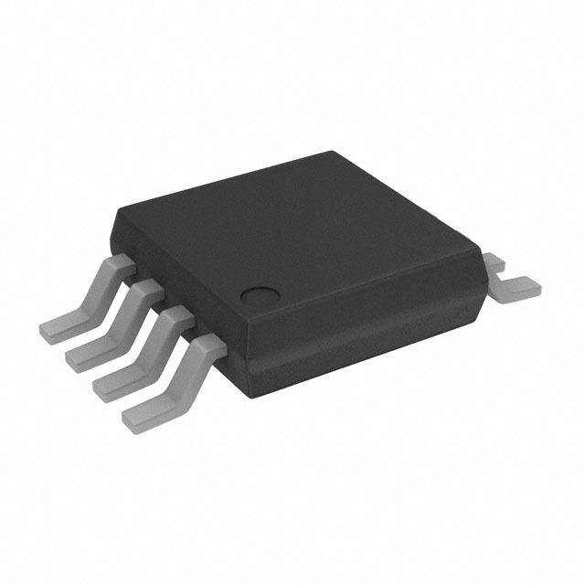
| 描述 | IC OPAMP JFET 1.9MHZ RRO 8MSOP精密放大器 SGL-Supply RR Lo Pwr FET-Inpt |
| 产品分类 | Linear - Amplifiers - Instrumentation, OP Amps, Buffer Amps集成电路 - IC |
| 品牌 | Analog Devices |
| 产品手册 | |
| 产品图片 |
|
| rohs | 符合RoHS无铅 / 符合限制有害物质指令(RoHS)规范要求 |
| 产品系列 | 放大器 IC,精密放大器,Analog Devices AD820ARMZ-R7- |
| 数据手册 | |
| 产品型号 | AD820ARMZ-R7 |
| 产品培训模块 | http://www.digikey.cn/PTM/IndividualPTM.page?site=cn&lang=zhs&ptm=30008http://www.digikey.cn/PTM/IndividualPTM.page?site=cn&lang=zhs&ptm=26202 |
| 产品种类 | 精密放大器 |
| 供应商器件封装 | 8-MSOP |
| 关闭 | No |
| 其它名称 | AD820ARMZ-R7-ND |
| 包装 | 带卷 (TR) |
| 压摆率 | 3 V/µs |
| 双重电源电压 | +/- 3 V, +/- 5 V, +/- 9 V, +/- 12 V, +/- 15 V |
| 商标 | Analog Devices |
| 增益带宽生成 | 1.9 MHz |
| 增益带宽积 | 1.9MHz |
| 安装类型 | 表面贴装 |
| 安装风格 | SMD/SMT |
| 封装 | Reel |
| 封装/外壳 | 8-TSSOP,8-MSOP(0.118",3.00mm 宽) |
| 封装/箱体 | MSOP-8 |
| 工作温度 | -40°C ~ 85°C |
| 工作电源电压 | 5 V to 36 V |
| 工厂包装数量 | 1000 |
| 放大器类型 | J-FET |
| 最大功率耗散 | 800 mW |
| 最大双重电源电压 | +/- 18 V |
| 最大工作温度 | + 85 C |
| 最小双重电源电压 | +/- 2.5 V |
| 最小工作温度 | - 40 C |
| 标准包装 | 1,000 |
| 电压-电源,单/双 (±) | 5 V ~ 36 V, ±2.5 V ~ 18 V |
| 电压-输入失调 | 400µV |
| 电压增益dB | 120 dB |
| 电流-电源 | 700µA |
| 电流-输入偏置 | 2pA |
| 电流-输出/通道 | 20mA |
| 电源电压-最大 | 36 V |
| 电源电压-最小 | 5 V |
| 电源电流 | 900 uA |
| 电源类型 | Single, Dual |
| 电路数 | 1 |
| 系列 | AD820 |
| 视频文件 | http://www.digikey.cn/classic/video.aspx?PlayerID=1364138032001&width=640&height=505&videoID=2245193153001http://www.digikey.cn/classic/video.aspx?PlayerID=1364138032001&width=640&height=505&videoID=2245193159001 |
| 转换速度 | 3 V/us at 5 V |
| 输入补偿电压 | 100 uV |
| 输出类型 | Rail to Rail Output |
| 通道数量 | 1 Channel |


- 商务部:美国ITC正式对集成电路等产品启动337调查
- 曝三星4nm工艺存在良率问题 高通将骁龙8 Gen1或转产台积电
- 太阳诱电将投资9.5亿元在常州建新厂生产MLCC 预计2023年完工
- 英特尔发布欧洲新工厂建设计划 深化IDM 2.0 战略
- 台积电先进制程称霸业界 有大客户加持明年业绩稳了
- 达到5530亿美元!SIA预计今年全球半导体销售额将创下新高
- 英特尔拟将自动驾驶子公司Mobileye上市 估值或超500亿美元
- 三星加码芯片和SET,合并消费电子和移动部门,撤换高东真等 CEO
- 三星电子宣布重大人事变动 还合并消费电子和移动部门
- 海关总署:前11个月进口集成电路产品价值2.52万亿元 增长14.8%


PDF Datasheet 数据手册内容提取
Single-Supply, Rail-to-Rail, Low Power, FET Input Op Amp AD820 FEATURES PIN CONFIGURATIONS True single-supply operation NULL 1 AD820 8 NC Output swings rail-to-rail Input voltage range extends below ground –IN 2 7 +VS Single-supply capability from 5 V to 30 V +IN 3 6 VOUT Dual-supply capability from ±2.5 V to ±15 V –VS 4 TOP VIEW 5 NULL ExcCealpleanctit liovaed lo dardiv der ive up to 350 pF NC( =N oNtO to C SOcNaNleE)CT 00873-001 Figure 1. 8-Lead PDIP Minimum output current of 15 mA Excellent ac performance for low power NC 1 AD820 8 NC 800 μA maximum quiescent current Unity-gain bandwidth: 1.8 MHz –IN 2 7 +VS Slew rate of 3 V/μs +IN 3 6 VOUT Excellent dc performance –VS 4 TOP VIEW 5 NC 28 0μ0V μ/°VC mtyapxiicmalu omff sinept uvot lotfafgseet d vroifltt a ge NC( =N oNtO to C SOcNaNleE)CT 00873-002 Figure 2. 8-Lead SOIC_N and 8-Lead MSOP 25 pA maximum input bias current Low noise: 13 nV/√Hz @ 10 kHz APPLICATIONS Battery-powered precision instrumentation Photodiode preamps Active filters 12-bit to 14-bit data acquisition systems Medical instrumentation Low power references and regulators GENERAL DESCRIPTION The AD820 is a precision, low power FET input op amp that The AD820 is available in two performance grades. The A and can operate from a single supply of 5 V to 36 V, or dual supplies B grades are rated over the industrial temperature range of of ±2.5 V to ±18 V. It has true single-supply capability, with an −40°C to +85°C. The AD820 is offered in three 8-lead package input voltage range extending below the negative rail, allowing options: plastic DIP (PDIP), surface mount (SOIC) and (MSOP). the AD820 to accommodate input signals below ground in the single-supply mode. Output voltage swing extends to within 1V 1V 20µs 10 mV of each rail, providing the maximum output dynamic range. 100 Offset voltage of 800 μV maximum, offset voltage drift of 90 2 μV/°C, typical input bias currents below 25 pA, and low input voltage noise provide dc precision with source impedances up to 1 GΩ. 1.8 MHz unity gain bandwidth, −93 dB THD at 10 kHz, and 3 V/μs slew rate are provided for a low supply current of 800 μA. The AD820 drives up to 350 pF of direct capacitive load and provides a minimum output current of 10 15 mA. This allows the amplifier to handle a wide range of load 0% cthoen doiuttisotnasn.d Tinhgis lcooamd bdirnivaeti coanp oafb ialcit ya,n rde sducl tps eirnf oarnm eaxncceep,t ipolnusa lly 1V 00873-004 versatile amplifier for the single-supply user. Figure 3. Gain-of-2 Amplifier; V = 5 V, 0 V, V = 2.5 V Sine Centered at 1.25 V S IN Rev. H Information furnished by Analog Devices is believed to be accurate and reliable. However, no responsibility is assumed by Analog Devices for its use, nor for any infringements of patents or other One Technology Way, P.O. Box 9106, Norwood, MA 02062-9106, U.S.A. rights of third parties that may result from its use. Specifications subject to change without notice. No license is granted by implication or otherwise under any patent or patent rights of Analog Devices. Tel: 781.329.4700 www.analog.com Trademarks and registered trademarks are the property of their respective owners. Fax: 781.461.3113 ©1996–2011 Analog Devices, Inc. All rights reserved.
AD820 TABLE OF CONTENTS Features .............................................................................................. 1 Applications Information .............................................................. 16 Applications ....................................................................................... 1 Input Characteristics .................................................................. 16 Pin Configurations ........................................................................... 1 Output Characteristics............................................................... 17 General Description ......................................................................... 1 Single-Supply Half-Wave and Full-Wave Rectifiers .............. 17 Revision History ............................................................................... 2 4.5 V Low Dropout, Low Power Reference ............................. 18 Specifications ..................................................................................... 3 Low Power, 3-Pole, Sallen Key Low-Pass Filter ...................... 18 Absolute Maximum Ratings ............................................................ 9 Offset Voltage Adjustment ............................................................ 19 Thermal Resistance ...................................................................... 9 Outline Dimensions ....................................................................... 20 ESD Caution .................................................................................. 9 Ordering Guide .......................................................................... 21 Typical Performance Characteristics ........................................... 10 REVISION HISTORY 3/11—Rev. G to Rev. H Added Table 5; Renumbered Sequentially ..................................... 9 Changes to Figure 43 ...................................................................... 18 Changes to Figure 26 ...................................................................... 13 Changes to Figure 27 ...................................................................... 14 2/10—Rev. F to Rev. G Changed Application Notes Section to Applications Changes to Features Section............................................................ 1 Information Section ....................................................................... 16 Changes to Open-Loop Gain Parameter ....................................... 3 Changes to Figure 40, Figure 41, and Figure 42 ......................... 17 Changes to Input Voltage Parameter ............................................. 9 Changes to Figure 44 ...................................................................... 18 Updated Outline Dimensions ....................................................... 20 Moved Offset Voltage Adjustment Section ................................. 19 Updated Outline Dimensions ....................................................... 20 11/08—Rev. E to Rev. F Added Figure 49; Renumbered Sequentially .............................. 21 Added 8-Lead MSOP ......................................................... Universal Changes to Ordering Guide .......................................................... 21 Changes to Features Section, Figure 2 Caption, and General Description Section .......................................................................... 1 2/07—Rev. D to Rev. E Changes to Settling Time Parameter, Common-Mode Voltage Updated Format .................................................................. Universal Range Parameter, and Power Supply Rejection Parameter in Updated Outline Dimensions ....................................................... 21 Table 1 ................................................................................................ 3 Changes to the Ordering Guide ................................................... 22 Changes to Settling Time Parameter, Common-Mode Voltage Range Parameter, and Power Supply Rejection Parameter in 5/02—Rev. C to Rev. D Table 2 ................................................................................................ 5 Change to SOIC Package (R-8) Drawing .................................... 15 Changes to Settling Time Parameter, Common-Mode Voltage Edits to Features................................................................................. 1 Range Parameter, and Power Supply Rejection Parameter in Edits to Product Description ........................................................... 1 Table 3 ................................................................................................ 7 Delete Specifications for AD820A-3 V ........................................... 5 Changes to Table 4 ............................................................................ 9 Edits to Ordering Guide ................................................................... 6 Added Thermal Resistance Section ............................................... 9 Edits to Typical Performance Characteristics ................................ 8 Rev. H | Page 2 of 24
AD820 SPECIFICATIONS V = 0 V, 5 V @ T = 25°C, V = 0 V, V = 0.2 V, unless otherwise noted. S A CM OUT Table 1. AD820A AD820B Parameter Conditions Min Typ Max Min Typ Max Unit DC PERFORMANCE Initial Offset 0.1 0.8 0.1 0.4 mV Maximum Offset over Temperature 0.5 1.2 0.5 0.9 mV Offset Drift 2 2 μV/°C Input Bias Current V = 0 V to 4 V 2 25 2 10 pA CM At T 0.5 5 0.5 2.5 nA MAX Input Offset Current 2 20 2 10 pA At T 0.5 0.5 nA MAX Open-Loop Gain V = 0.2 V to 4 V OUT R = 100 kΩ 400 1000 500 1000 V/mV L T to T 400 400 V/mV MIN MAX R = 10 kΩ 80 150 80 150 V/mV L T to T 80 80 V/mV MIN MAX R = 1 kΩ 15 30 15 30 V/mV L T to T 10 10 V/mV MIN MAX NOISE/HARMONIC PERFORMANCE Input Voltage Noise f = 0.1 Hz to 10 Hz 2 2 μV p-p f = 10 Hz 25 25 nV/√Hz f = 100 Hz 21 21 nV/√Hz f = 1 kHz 16 16 nV/√Hz f = 10 kHz 13 13 nV/√Hz Input Current Noise f = 0.1 Hz to 10 Hz 18 18 fA p-p f = 1 kHz 0.8 0.8 fA/√Hz Harmonic Distortion R = 10 kΩ to 2.5 V L f = 10 kHz V = 0.25 V to 4.75 V −93 −93 dB OUT DYNAMIC PERFORMANCE Unity Gain Frequency 1.8 1.8 MHz Full Power Response V p-p = 4.5 V 210 210 kHz OUT Slew Rate 3 3 V/μs Settling Time V = 0.2 V to 4.5 V OUT To 0.1% 1.4 1.4 μs To 0.01% 1.8 1.8 μs INPUT CHARACTERISTICS Common-Mode Voltage Range1 T to T −0.2 +4 –0.2 +4 V MIN MAX CMRR V = 0 V to 2 V 66 80 72 80 dB CM T to T 66 66 dB MIN MAX Input Impedance Differential 1013||0.5 1013||0.5 Ω||pF Common Mode 1013||2.8 1013||2.8 Ω||pF Rev. H | Page 3 of 24
AD820 AD820A AD820B Parameter Conditions Min Typ Max Min Typ Max Unit OUTPUT CHARACTERISTICS Output Saturation Voltage2 V − V I = 20 μA 5 7 5 7 mV OL EE SINK T to T 10 10 mV MIN MAX V − V I = 20 μA 10 14 10 14 mV CC OH SOURCE T to T 20 20 mV MIN MAX V − V I = 2 mA 40 55 40 55 mV OL EE SINK T to T 80 80 mV MIN MAX V − V I = 2 mA 80 110 80 110 mV CC OH SOURCE T to T 160 160 mV MIN MAX V − V I = 15 mA 300 500 300 500 mV OL EE SINK T to T 1000 1000 mV MIN MAX V − V I = 15 mA 800 1500 800 1500 mV CC OH SOURCE T to T 1900 1900 mV MIN MAX Operating Output Current 15 15 mA T to T 12 12 mA MIN MAX Short-Circuit Current 25 25 mA Capacitive Load Drive 350 350 pF POWER SUPPLY Quiescent Current T to T 620 800 620 800 μA MIN MAX Power Supply Rejection V+ = 5 V to 15 V 70 80 66 80 dB T to T 70 66 dB MIN MAX 1 This is a functional specification. Amplifier bandwidth decreases when the input common-mode voltage is driven in the range ((V+) − 1 V) to V+. Common-mode error voltage is typically less than 5 mV with the common-mode voltage set at 1 V below the positive supply. 2 V − V is defined as the difference between the lowest possible output voltage (V ) and the negative voltage supply rail (V ). V − V is defined as the difference OL EE OL EE CC OH between the highest possible output voltage (V ) and the positive supply voltage (V ). OH CC Rev. H | Page 4 of 24
AD820 V = ±5 V @ T = 25°C, V = 0 V, V = 0 V, unless otherwise noted. S A CM OUT Table 2. AD820A AD820B Parameter Conditions Min Typ Max Min Typ Max Unit DC PERFORMANCE Initial Offset 0.1 0.8 0.3 0.4 mV Maximum Offset over Temperature 0.5 1.5 0.5 1 mV Offset Drift 2 2 μV/°C Input Bias Current V = −5 V to +4 V 2 25 2 10 pA CM At T 0.5 5 0.5 2.5 nA MAX Input Offset Current 2 20 2 10 pA At T 0.5 0.5 nA MAX Open-Loop Gain V = −4 V to +4 V OUT R = 100 kΩ 400 1000 400 1000 V/mV L T to T 400 400 V/mV MIN MAX R = 10 kΩ 80 150 80 150 V/mV L T to T 80 80 V/mV MIN MAX R = 1 kΩ 20 30 20 30 V/mV L T to T 10 10 V/mV MIN MAX NOISE/HARMONIC PERFORMANCE Input Voltage Noise f = 0.1 Hz to 10 Hz 2 2 μV p-p f = 10 Hz 25 25 nV/√Hz f = 100 Hz 21 21 nV/√Hz f = 1 kHz 16 16 nV/√Hz f = 10 kHz 13 13 nV/√Hz Input Current Noise f = 0.1 Hz to 10 Hz 18 18 fA p-p f = 1 kHz 0.8 0.8 fA/√Hz Harmonic Distortion R = 10 kΩ L f = 10 kHz V = ±4.5 V −93 −93 dB OUT DYNAMIC PERFORMANCE Unity Gain Frequency 1.9 1.8 MHz Full Power Response V p-p = 9 V 105 105 kHz OUT Slew Rate 3 3 V/μs Settling Time V = 0 V to ±4.5 V OUT To 0.1% 1.4 1.4 μs To 0.01% 1.8 1.8 μs INPUT CHARACTERISTICS Common-Mode Voltage Range1 T to T −5.2 +4 −5.2 +4 V MIN MAX CMRR V = −5 V to +2 V 66 80 72 80 dB CM T to T 66 66 dB MIN MAX Input Impedance Differential 1013||0.5 1013||0.5 Ω||pF Common Mode 1013||2.8 1013||2.8 Ω||pF Rev. H | Page 5 of 24
AD820 AD820A AD820B Parameter Conditions Min Typ Max Min Typ Max Unit OUTPUT CHARACTERISTICS Output Saturation Voltage2 V − V I = 20 μA 5 7 5 7 mV OL EE SINK T to T 10 10 mV MIN MAX V − V I = 20 μA 10 14 10 14 mV CC OH SOURCE T to T 20 20 mV MIN MAX V − V I = 2 mA 40 55 40 55 mV OL EE SINK T to T 80 80 mV MIN MAX V − V I = 2 mA 80 110 80 110 mV CC OH SOURCE T to T 160 160 mV MIN MAX V − V I = 15 mA 300 500 300 500 mV OL EE SINK T to T 1000 1000 mV MIN MAX V − V I = 15 mA 800 1500 800 1500 mV CC OH SOURCE T to T 1900 1900 mV MIN MAX Operating Output Current 15 15 mA T to T 12 12 mA MIN MAX Short-Circuit Current 30 30 mA Capacitive Load Drive 350 350 pF POWER SUPPLY Quiescent Current T to T 650 800 620 800 μA MIN MAX Power Supply Rejection V+ = 5 V to 15 V 70 80 70 80 dB T to T 70 70 dB MIN MAX 1 This is a functional specification. Amplifier bandwidth decreases when the input common-mode voltage is driven in the range ((V+) − 1 V) to V+. Common-mode error voltage is typically less than 5 mV with the common-mode voltage set at 1 V below the positive supply. 2 V − V is defined as the difference between the lowest possible output voltage (V ) and the negative voltage supply rail (V ). V − V is defined as the difference OL EE OL EE CC OH between the highest possible output voltage (V ) and the positive supply voltage (V ). OH CC Rev. H | Page 6 of 24
AD820 V = ±15 V @ T = 25°C, V = 0 V, V = 0 V, unless otherwise noted. S A CM OUT Table 3. AD820A AD820B Parameter Conditions Min Typ Max Min Typ Max Unit DC PERFORMANCE Initial Offset 0.4 2 0.3 1.0 mV Maximum Offset over Temperature 0.5 3 0.5 2 mV Offset Drift 2 2 μV/°C Input Bias Current V = 0 V 2 25 2 10 pA CM V = −10 V 40 40 pA CM At T V = 0 V 0.5 5 0.5 2.5 nA MAX CM Input Offset Current 2 20 2 10 pA At T 0.5 0.5 nA MAX Open-Loop Gain V = −10 V to +10 V OUT R = 100 kΩ 500 2000 500 2000 V/mV L T to T 500 500 V/mV MIN MAX R = 10 kΩ 100 500 100 500 V/mV L T to T 100 100 V/mV MIN MAX R = 1 kΩ 30 45 30 45 V/mV L T to T 20 20 V/mV MIN MAX NOISE/HARMONIC PERFORMANCE Input Voltage Noise f = 0.1 Hz to 10 Hz 2 2 μV p-p f = 10 Hz 25 25 nV/√Hz f = 100 Hz 21 21 nV/√Hz f = 1 kHz 16 16 nV/√Hz f = 10 kHz 13 13 nV/√Hz Input Current Noise f = 0.1 Hz to 10 Hz 18 18 fA p-p f = 1 kHz 0.8 0.8 fA/√Hz Harmonic Distortion R = 10 kΩ L f = 10 kHz V = ±10 V −85 −85 dB OUT DYNAMIC PERFORMANCE Unity Gain Frequency 1.9 1.9 MHz Full Power Response V p-p = 20 V 45 45 kHz OUT Slew Rate 3 3 V/μs Settling Time V = 0 V to ±10 V OUT To 0.1% 4.1 4.1 μs To 0.01% 4.5 4.5 μs INPUT CHARACTERISTICS Common-Mode Voltage Range1 T to T −15.2 +14 −15.2 +14 V MIN MAX CMRR V = –15 V to +12 V 70 80 74 90 dB CM T to T 70 74 dB MIN MAX Input Impedance Differential 1013||0.5 1013||0.5 Ω||pF Common Mode 1013||2.8 1013||2.8 Ω||pF Rev. H | Page 7 of 24
AD820 AD820A AD820B Parameter Conditions Min Typ Max Min Typ Max Unit OUTPUT CHARACTERISTICS Output Saturation Voltage2 V − V I = 20 μA 5 7 5 7 mV OL EE SINK T to T 10 10 mV MIN MAX V − V I = 20 μA 10 14 10 14 mV CC OH SOURCE T to T 20 20 mV MIN MAX V − V I = 2 mA 40 55 40 55 mV OL EE SINK T to T 80 80 mV MIN MAX V − V I = 2 mA 80 110 80 110 mV CC OH SOURCE T to T 160 160 mV MIN MAX V − V I = 15 mA 300 500 300 500 mV OL EE SINK T to T 1000 1000 mV MIN MAX V − V I = 15 mA 800 1500 800 1500 mV CC OH SOURCE T to T 1900 1900 mV MIN MAX Operating Output Current 20 20 mA T to T 15 15 mA MIN MAX Short-Circuit Current 45 45 mA Capacitive Load Drive 350 350 pF POWER SUPPLY Quiescent Current T to T 700 900 700 900 μA MIN MAX Power Supply Rejection V+ = 5 V to 15 V 70 80 70 80 dB T to T 70 70 dB MIN MAX 1 This is a functional specification. Amplifier bandwidth decreases when the input common-mode voltage is driven in the range ((V+) − 1 V) to V+. Common-mode error voltage is typically less than 5 mV with the common-mode voltage set at 1 V below the positive supply. 2 V − V is defined as the difference between the lowest possible output voltage (V ) and the negative voltage supply rail (V ). V − V is defined as the difference OL EE OL EE CC OH between the highest possible output voltage (V ) and the positive supply voltage (V ). OH CC Rev. H | Page 8 of 24
AD820 ABSOLUTE MAXIMUM RATINGS THERMAL RESISTANCE Table 4. Parameter Rating θ is specified for the worst-case conditions, that is, a device JA Supply Voltage ±18 V soldered in a circuit board for surface-mount packages. Internal Power Dissipation Table 5. Thermal Resistance 8-Lead PDIP (N) 1.6 W Package Type θ Unit 8-Lead SOIC_N (R) 1.0 W JA 8-Lead PDIP (N) 90 °C/W 8-Lead MSOP (RM) 0.8 W 8-Lead SOIC_N (R) 160 °C/W Input Voltage1 ((V+) + 0.2 V) to (V−) − 20 V 8-Lead MSOP (RM) 190 °C/W Output Short-Circuit Duration Indefinite Differential Input Voltage ±30 V Stresses above those listed under Absolute Maximum Ratings Storage Temperature Range may cause permanent damage to the device. This is a stress 8-Lead PDIP (N) −65°C to +125°C rating only; functional operation of the device at these or any 8-Lead SOIC_N (R) −65°C to +150°C other conditions above those indicated in the operational 8-Lead MSOP (RM) −65°C to +150°C section of this specification is not implied. Exposure to absolute Operating Temperature Range maximum rating conditions for extended periods may affect AD820A/AD820B −40°C to +85°C device reliability. Lead Temperature(Soldering, 60 sec) 260°C 1 See Input Characteristics section. ESD CAUTION Rev. H | Page 9 of 24
AD820 TYPICAL PERFORMANCE CHARACTERISTICS 50 5 VS = 0V, 5V 40 A) p UNITS 30 RENT ( F R MBER O 20 BIAS CU 0 VS = 0V, +5V AND ±5V NU PUT VS = ±5V N I 10 0 00873-005 –5 00873-008 –0.5 –0.4 –0.3 –0.2 –0.1 0 0.1 0.2 0.3 0.4 0.5 –5 –4 –3 –2 –1 0 1 2 3 4 5 OFFSET VOLTAGE (mV) COMMON-MODE VOLTAGE (V) Figure 4. Typical Distribution of Offset Voltage (248 Units) Figure 7. Input Bias Current vs. Common-Mode Voltage; V = +5 V, 0 V and V = ±5 V S S 48 1k VS = ±5V 40 VS = ±15V A) 100 p 32 T ( N E N R N BI 24 CUR 10 % I AS BI 16 UT P N 1 I 8 0 00873-006 0.1 00873-009 –10 –8 –6 –4 –2 0 2 4 6 8 10 –16 –12 –8 –4 0 4 8 12 16 OFFSET VOLTAGE DRIFT (µV/ºC) COMMON-MODE VOLTAGE (V) Figure 5. Typical Distribution of Offset Voltage Drift (120 Units) Figure 8. Input Bias Current vs. Common-Mode Voltage; V = ±15 V S 100k 50 45 10k 40 A) p T ( 1k UNITS 3350 URREN F C 100 R O 25 AS E BI NUMB 2105 INPUT 10 1 1050 00873-007 0.120 40 60 80 100 120 14000873-010 0 1 2 3 4 5 6 7 8 9 10 TEMPERATURE (ºC) INPUT BIAS CURRENT (pA) Figure 6. Typical Distribution of Input Bias Current (213 Units) Figure 9. Input Bias Current vs. Temperature; V = 5 V, V = 0 V S CM Rev. H | Page 10 of 24
AD820 10M 40 POSITIVE AIN (V/V) 1M VS = ±15V LTAGE (µV) 20 RL = 20kΩ RL = 2kΩ RNREAAGIILLATIVE OOP G VS = 0V, +5V OR VO 0 PROAISLITIVE L R OPEN-100k NPUT ER –20 PROAISLITIVE NREAGILATIVE I 10k 00873-011 –40 RL = 100kΩ NEGATIVE RAIL 00873-014 100 1k 10k 100k 0 60 120 180 240 300 LOAD RESISTANCE (Ω) OUTPUT VOLTAGE FROM RAILS (mV) Figure 10. Open-Loop Gain vs. Load Resistance Figure 13. Input Error Voltage vs. Output Voltage Within 300 mV of Either Supply Rail for Various Resistive Loads; V = ±5 V S 10M 1k Hz) N (V/V) 1M RL = 100kΩ VVSS == 0±V1,5 +V5V SE (nV/√ 100 AI OI OP G RL = 10kΩ VS = ±15V GE N O A OPEN-L100k VS = 0V, +5V T VOLT 10 VS = ±15V PU RL = 600Ω IN 10k VS = 0V, +5V 00873-012 1 00873-015 –60 –40 –20 0 20 40 60 80 100 120 140 1 10 100 1k 10k TEMPERATURE (ºC) FREQUENCY (Hz) Figure 11. Open-Loop Gain vs. Temperature Figure 14. Input Voltage Noise vs. Frequency 300 –40 –50 RL = 10kΩ 200 ACL = –1 V) µ E ( –60 TAG 100 RL = 10kΩ RL = 100kΩ R VOL 0 D (dB) –70 O H R T –80 ER VS = ±15V; VOUT = 20V p-p T –100 U –90 NP VS = ±5V; VOUT = 9V p-p I ––230000 RL = 600Ω 00873-013 ––110100 VS = 0V, +5V; VOUT = 4.5V p-p 00873-016 –16 –12 –8 –4 0 4 8 12 16 100 1k 10k 100k OUTPUT VOLTAGE (V) FREQUENCY (Hz) Figure 12. Input Error Voltage vs. Output Voltage for Resistive Loads Figure 15. Total Harmonic Distortion vs. Frequency Rev. H | Page 11 of 24
AD820 100 100 100 90 B) 80 PHASE 80 EES) ON (dB) 8700 OP GAIN (d 6400 GAIN 6400 GIN (DEGR E REJECTI 6500 VS = 0V, +5V VS = ±15V O R D OPEN-L 20 20 PHASE MA MMON-MO 4300 0 0 CO 20 –20 RCLL == 21k0Ω0pF –20 100 00873-020 10 100 1kFREQU1E0NkCY (Hz)100k 1M 10M 00873-017 10 100 1kFREQU1E0NkCY (Hz)100k 1M 10M Figure 16. Open-Loop Gain and Phase Margin vs. Frequency Figure 19. Common-Mode Rejection vs. Frequency 1k 5 ACL = +1 V) VS = ±15V m 100 E ( 4 G Ω) A CE ( OLT AN 10 R V 3 NREAGILATIVE PROAISLITIVE D O MPE ERR UT I 1 DE 2 TP MO +25ºC OU N- O 0.1 MM 1 +125ºC +125ºC O 0.01 00873-018 C 0 –55ºC –55ºC 00873-021 100 1k 10k 100k 1M 10M –1 0 1 2 3 FREQUENCY (Hz) COMMON-MODE VOLTAGE FROM SUPPLY RAILS (V) Figure 17. Output Impedance vs. Frequency Figure 20. Absolute Common-Mode Error vs. Common-Mode Voltage from Supply Rails (V − V ) S CM 16 1k 12 V) m O ±V 8 1% GE ( T A M 0 4 OLT 100 O V WING FR 0 0.1% 0.01% ERROR RATION VS – VOH UT S –4 SATU 10 VOL – VS OUTP –8 1% TPUT U ––1126 00873-019 O 1 00873-022 0 1 2 3 4 5 0.001 0.01 0.1 1 10 100 SETTLING TIME (µs) LOAD CURRENT (mA) Figure 18. Output Swing and Error vs. Settling Time Figure 21. Output Saturation Voltage vs. Load Current Rev. H | Page 12 of 24
AD820 1k 120 ISOURCE = 10mA 110 V) GE (m ISINK = 10mA N (dB) 10900 A O LT 100 TI 80 TION VO IISSOINUKR =C E1 m= A1mA Y REJEC 7600 +PSRR A L –PSRR TUR ISOURCE = 10µA UPP 50 T SA 10 ISINK = 10µA ER S 40 U W 30 UTP PO 20 O 1 00873-023 100 00873-026 –60 –40 –20 0 20 40 60 80 100 120 140 10 100 1k 10k 100k 1M 10M TEMPERATURE (ºC) FREQUENCY (Hz) Figure 22. Output Saturation Voltage vs. Temperature Figure 25. Power Supply Rejection vs. Frequency 80 30 RL = 2kΩ A) 70 m 25 NT LIMIT ( 6500 VS = ±15V–OUT GE (V) 20 VS = ±15V E A R T UR 40 VS = ±15V OL 15 C V RCUIT 30 VS = 0V, +5V –+ UTPUT 10 CI O ORT- 20 VS = 0V, +5V + VS = 0V, +5V H 5 S 100 00873-024 0 00873-027 –60 –40 –20 0 20 40 60 80 100 120 140 10k 100k 1M 10M TEMPERATURE (ºC) FREQUENCY (Hz) Figure 23. Short-Circuit Current Limit vs. Temperature Figure 26. Large Signal Frequency Response 800 T = +125ºC 700 T = +25ºC A) 600 T (µ T = –55ºC EN 500 R R U C 400 T N E C 300 S E UI Q 200 1000 00873-025 0 4 8 12 16 20 24 28 32 36 TOTAL SUPPLY VOLTAGE (V) Figure 24. Quiescent Current vs. Supply Voltage over Different Temperatures Rev. H | Page 13 of 24
AD820 5V 5µs +VS 100 90 0.01µF + 3 + 7 VI–N AD820 6 + 2 – 4 0.01µF RL 100pF V–OUT –VS 00873-028 01%0 00873-031 Figure 27. Unity-Gain Follower, Used for Figure 28 Through Figure 32 Figure 30. Large Signal Response Unity-Gain Follower; V = ±15 V, R = 10 kΩ S L 5V 10µs 10mV 500ns 100 100 90 90 10 10 0% 0% 00873-029 00873-032 Figure 28. 20 V, 25 kHz Sine Input; Unity-Gain Follower; R = 600 Ω, V = ±15 V Figure 31. Small Signal Response Unity-Gain Follower; V = ±15 V, R = 10 kΩ L S S L 1V 2µs 1V 2µs 100 100 90 90 10 10 GND 0% GND 0% 00873-030 00873-033 Figure 29. V = 5 V, 0 V; Unity-Gain Follower Response to 0 V to 4 V Step Figure 32. V = 5 V, 0 V; Unity-Gain Follower Response to 0 V to 5 V Step S S Rev. H | Page 14 of 24
AD820 10kΩ 20kΩ +VS VIN + 0.01µF +VS V–OUT VIN 3 A+D7820 6 + 2 – 7 0.01µF 2 – RL 100pF V–OUT AD820 6 4 00873-034 3 + 4 RL 100pF 00873-035 Figure 33. Unity-Gain Follower, Used for Figure 34 Figure 35. Gain-of-2 Inverter, Used for Figure 36 and Figure 37 10mV 2µs 1V 2µS 100 100 90 90 10 10 GND 0% GND 0% 00873-037 00873-036 Figure 34. V = 5 V, 0 V; Unity-Gain Follower Response to 40 mV Step Figure 36. V = 5 V, 0 V; Gain-of-2 Inverter Response to 2.5 V Step, S S Centered 40 mV Above Ground Centered −1.25 V Below Ground 10mV 2µs 100 90 10 GND 0% 00873-038 Figure 37. V = 5 V, 0 V; Gain-of-2 Inverter Response to 20 mV Step, Centered S 20 mV Below Ground Rev. H | Page 15 of 24
AD820 APPLICATIONS INFORMATION INPUT CHARACTERISTICS 1V 2µs In the AD820, N-channel JFETs are used to provide a low offset, low noise, high impedance input stage. Minimum input common- 100 mode voltage extends from 0.2 V below –V to 1 V less than 90 S +V. Driving the input voltage closer to the positive rail causes a S loss of amplifier bandwidth (as can be seen by comparing the large signal responses shown in Figure 29 and Figure 32) and increased common-mode voltage error, as illustrated in Figure 20. 10 The AD820 does not exhibit phase reversal for input voltages GND 0% up to and including +V. Figure 38a shows the response of an S 1V AD820 voltage follower to a 0 V to 5 V (+V) square wave input. S The input and output are superimposed. The output polarity (a) tracks the input polarity up to +V with no phase reversal. The S reduced bandwidth above a 4 V input causes the rounding of 1V 1V 10µs the output waveform. For input voltages greater than +V, a S resistor in series with the AD820 positive input prevents phase 100 reversal, at the expense of greater input voltage noise. This is +VS 90 illustrated in Figure 38b. Because the input stage uses N-channel JFETs, input current during normal operation is negative; the current flows out from the input terminals. If the input voltage is driven more positive than +V − 0.4 V, the input current reverses direction as internal S 10 device junctions become forward biased. This is illustrated in GND 0% Figure 7. 1V A current-limiting resistor should be used in series with the input of the AD820 if there is a possibility of the input voltage (b) exceeding the positive supply by more than 300 mV, or if an 5V input voltage is applied to the AD820 when ±V = 0 V. The S RP amplifier can be damaged if left in that condition for more than + + 10 seconds. A 1 kΩ resistor allows the amplifier to withstand up VI–N AD820 + to 10 V of continuous overvoltage, and increases the input – VOUT – voltage noise by a negligible amount. 00873-039 Input voltages less than −V are a completely different story. S Figure 38. (a) Response with RP = 0 Ω; VIN from 0 V to +VS The amplifier can safely withstand input voltages 20 V below (b) V = 0 V to +V + 200 mV, IN S the negative supply voltage as long as the total voltage from VOUT = 0 V to +VS, RP = 49.9 kΩ the positive supply to the input terminal is less than 36 V. In 100k WHENEVER JOHNSON NOISE IS GREATER THAN addition, the input stage typically maintains picoamp level AMPLIFIER NOISE, AMPLIFIER NOISE CAN BE input currents across that input voltage range. s) 10k CONSIDERED NEGLIGIBLE FOR APPLICATION. m The AD820 is designed for 13 nV/√Hz wideband input voltage V r 1kHz µ noise and maintains low noise performance to low frequencies OISE ( 1k RESISTOR JOHNSON (refer to Figure 14). This noise performance, along with the N NOISE E 100 AD820 low input current and current noise, means that the G A T AD820 contributes negligible noise for applications with source L O V 10 resistances greater than 10 kΩ and signal bandwidths greater T than 1 kHz. This is illustrated in Figure 39. NPU 10Hz I 1 0.1 AMPLIFIENRO-GISEENERATED 00873-040 10k 100k 1M 10M 100M 1G 10G SOURCE IMPEDANCE (Ω) Figure 39. Total Noise vs. Source Impedance Rev. H | Page 16 of 24
AD820 OUTPUT CHARACTERISTICS 5 The AD820 unique bipolar rail-to-rail output stage swings within 5 mV of the negative supply and 10 mV of the positive 4 ssuatpuprlayt iwonit hre nsois teaxntceern oafl trhees iAstDiv8e2 l0o aids .4 T0 hΩe saopuprrcoixnigm aanted o2u0t pΩu t PI+ )PF 1 sinking. This can be used to estimate output saturation voltage N ( AI 3 when driving heavier current loads. For instance, when sourcing G E 5 mA, the saturation voltage to the positive supply rail is 200 mV; OIS N when sinking 5 mA, the saturation voltage to the negative rail 2 is 100 mV. The open-loop gain characteristic of the amplifier changes as a function of resistive load, as shown in Figure 10 through 1 300 1k 3k 10k 30k Figure 13. For load resistances over 20 kΩ, the AD820 input CAPACITIVE LOAD FOR 20º PHASE MARGIN (pF) error voltage is virtually unchanged until the output voltage is driven to 180 mV of either supply. + If the AD820 output is driven hard against the output saturation – voltage, it recovers within 2 μs of the input returning to the linear operating region of the amplifier. RF Danicreec ot fc tahpea caimtipveli flioeard t oin ftoerrmac tasn w aidthd itthioen eaflf epcotliev ein o uthtpe uatm implpifeiedr- R1 00873-042 feedback loop, which can cause excessive peaking on the pulse Figure 41. Noise Gain vs. Capacitive Load Tolerance response or loss of stability. The worst case occurs when the Figure 42 shows a possible configuration for extending amplifier is used as a unity-gain follower. Figure 40 shows capacitance load drive capability for a unity-gain follower. With AD820 pulse response as a unity-gain follower driving 350 pF. these component values, the circuit drives 5000 pF with a 10% This amount of overshoot indicates approximately 20 degrees overshoot. of phase margin—the system is stable, but is nearing the edge. +VS Configurations with less loop gain, and as a result less loop 0.01µF bandwidth, are much less sensitive to capacitance load effects. Figure 41 is a plot of noise gain vs. the capacitive load that results + 3 + 7 in a 20 degree phase margin for the AD820. Noise gain is the VI–N AD820 6 100Ω + 2 – 0.01µF VOUT inverse of the feedback attenuation factor provided by the 4 – feedback network in use. –VS 20pF 100 20mV 2µs 20kΩ 00873-043 Figure 42. Extending Unity-Gain Follower Capacitive Load Capability 90 Beyond 350 pF SINGLE-SUPPLY HALF-WAVE AND FULL-WAVE RECTIFIERS An AD820 configured as a unity-gain follower and operated with a single supply can be used as a simple half-wave rectifier. 10 The AD820 inputs maintain picoamp level input currents even 0% when driven well below the negative supply. The rectifier puts 00873-041 tohvaetr b1e0h11a vΩio fro rto i ngpouotd v uosltea, gmesa ifnrotamin 1in Vg afrno minp tuhte ipmopsietdivaen scuep opf ly Figure 40. Small Signal Response of AD820 as Unity-Gain Follower Driving to 20 V below the negative supply. 350 pF Capacitive Load The full- and half-wave rectifier shown in Figure 43 operates as follows: when V is above ground, R1 is bootstrapped through IN the unity-gain follower, A1, and the loop of Amplifier A2. This forces the inputs of A2 to be equal; thus, no current flows through R1 or R2, and the circuit output tracks the input. When V is IN below ground, the output of A1 is forced to ground. The Rev. H | Page 17 of 24
AD820 noninverting input of Amplifier A2 sees the ground level output With a 1 mA load, this reference maintains the 4.5 V output of A1; therefore, A2 operates as a unity-gain inverter. The output at with a supply voltage down to 4.7 V. The amplitude of the Node C is then a full-wave rectified version of the input. Node B is recovery transient for a 1 mA to 10 mA step change in load a buffered half-wave rectified version of the input. Input voltages current is under 20 mV, and settles out in a few microseconds. up to ±18 V can be rectified, depending on the voltage supply used. Output voltage noise is less than 10 μV rms in a 25 kHz noise R1 R2 bandwidth. 100kΩ 100kΩ LOW POWER, 3-POLE, SALLEN KEY LOW-PASS +VS +VS 0.01µF FILTER A 0.01µF 2 – 7 The high input impedance of the AD820 makes it a good + 3 + 7 A2 6 + C selection for active filters. High value resistors can be used to VI–N A1 6 3 + AD820 FRUELCLT-IWFIAEVDE OUPUT construct low frequency filters with capacitors much less than 2 – AD820 4 – 1 μF. The AD820 picoamp level input currents contribute 4 minimal dc errors. B + Figure 45 shows an example of a 10 Hz three-pole Sallen Key HALF-WAVE RECTIFIED OUPUT filter. The high value used for R1 minimizes interaction with – signal source resistance. Pole placement in this version of the filter minimizes the Q associated with the two-pole section of the filter. This eliminates any peaking of the noise contribution of Resistor R1, Resistor R2, and Resistor R3, thus minimizing A 100 the inherent output voltage noise of the filter. 90 C2 0.022µF +VS B R1 R2 R3 0.01µF + 243kΩ 243kΩ 243kΩ 3 + 7 C 01%0 VI–N C0.1022µF C0.3022µF 2 A–D8200.016µF V+OUT 4 – 00873-045 –VS Figure 43. Single-Supply Half- and Full-Wave Rectifier 4.5 V LOW DROPOUT, LOW POWER REFERENCE 0 The rail-to-rail performance of the AD820 can be used to –10 provide low dropout performance for low power reference B) –20 circuits powered with a single low voltage supply. Figure 44 E (d –30 shows a 4.5 V reference using the AD820 and the AD680, a low NS O –40 power 2.5 V band gap reference. R2 and R3 set up the required SP E gain of 1.8 to develop the 4.5 V output. R1 and C2 form a low- N R –50 pass RC filter to reduce the noise contribution of the AD680. GAI –60 R 2O.U5VTPUT LTE –70 U2 4.5V FI –80 AD820 6 OUTPUT 5V 7 4 R902kΩ –1–0900 00873-047 2 + – (20kΩ) 0.1 1 10 100 1k 3 U1 6 2.5V ± 10mV 3 2 C3 FREQUENCY (Hz) AD680 R1 10µF/25V Figure 45. 10 Hz Sallen Key Low-Pass Filter C0.11µF 4 100kΩ C0.21µF FILM R1(20350kkΩΩ) RCEOFMMON 00873-046 Figure 44. Single Supply 4.5 V Low Dropout Reference Rev. H | Page 18 of 24
AD820 OFFSET VOLTAGE ADJUSTMENT The offset voltage of the AD820 is low, so external offset voltage +VS nulling is not usually required. Figure 46 shows the recommended 3 + 7 technique for the AD820 packaged in plastic DIP. Adjusting offset AD820 6 voltage in this manner changes the offset voltage temperature drift 2 – 5 1 by 4 μV/°C for every millivolt of induced offset. The null pins 20kΩ are not functional for the AD820 in the 8-lead SOIC and MSOP 4 packages. –VS 00873-044 Figure 46. Offset Null Rev. H | Page 19 of 24
AD820 OUTLINE DIMENSIONS 0.400 (10.16) 0.365 (9.27) 0.355 (9.02) 8 5 0.280 (7.11) 0.250 (6.35) 1 4 0.240 (6.10) 0.325 (8.26) 0.310 (7.87) 0.100 (2.54) 0.300 (7.62) BSC 0.060 (1.52) 0.195 (4.95) 0.210 (5.33) MAX 0.130 (3.30) MAX 0.115 (2.92) 0.015 0.150 (3.81) (0.38) 0.015 (0.38) 0.130 (3.30) MIN GAUGE 0.115 (2.92) SEATING PLANE 0.014 (0.36) PLANE 0.010 (0.25) 0.022 (0.56) 0.008 (0.20) 0.005 (0.13) 0.430 (10.92) 0.018 (0.46) MIN MAX 0.014 (0.36) 0.070 (1.78) 0.060 (1.52) 0.045 (1.14) COMPLIANTTO JEDEC STANDARDS MS-001 CONTROLLING DIMENSIONSARE IN INCHES; MILLIMETER DIMENSIONS (RCINEOFRPEANRREERENN LCTEEHA EODSNSEL MSY)AAAYNR BDEE AR CROOEU NNNFODIGETUDAR-POEPFDRFOA INSPC RWHIAH ETOEQL UFEIO VORAR LU EHSNAETL ISFN FLDOEEARSDIGSN.. 070606-A Figure 47. 8-Lead Plastic Dual In-Line Package [PDIP] Narrow Body (N-8) Dimensions shown in inches and (millimeters) 5.00(0.1968) 4.80(0.1890) 8 5 4.00(0.1574) 6.20(0.2441) 3.80(0.1497) 1 4 5.80(0.2284) 1.27(0.0500) 0.50(0.0196) BSC 1.75(0.0688) 0.25(0.0099) 45° 0.25(0.0098) 1.35(0.0532) 8° 0.10(0.0040) 0° COPLANARITY 0.51(0.0201) 0.10 SEATING 0.31(0.0122) 0.25(0.0098) 10..2470((00..00510507)) PLANE 0.17(0.0067) COMPLIANTTOJEDECSTANDARDSMS-012-AA RC(INEOFNPEATRRREOENNLCLTEIHNEOGSNDELISYM)AEANNRDSEIAORRNOESUNANORDETEDAIN-POMPFRIFLOLMPIMIRLELIATIMTEEERTFSEO;RIRNECUQHSUEDIVIINMAELDENENSSTIIOGSNNFS.OR 012407-A Figure 48. 8-Lead Standard Small Outline Package [SOIC_N] Narrow Body (R-8) Dimensions shown in millimeters and (inches) Rev. H | Page 20 of 24
AD820 3.20 3.00 2.80 8 5 5.15 3.20 4.90 3.00 4.65 2.80 1 4 PIN1 IDENTIFIER 0.65BSC 0.95 15°MAX 0.85 1.10MAX 0.75 0.80 0.15 0.40 6° 0.23 0.55 CO0P.0L50A.1N0ARICTOYMPLIANT0.T25OJEDECSTA0°NDARDS0M.0O9-187-AA 0.40 10-07-2009-B Figure 49. 8-Lead Mini Small Outline Package [MSOP] (RM-8) Dimensions shown in millimeters ORDERING GUIDE Model1 Temperature Range Package Description Package Option Branding AD820AN −40°C to +85°C 8-Lead PDIP N-8 AD820ANZ −40°C to +85°C 8-Lead PDIP N-8 AD820AR −40°C to +85°C 8-Lead SOIC_N R-8 AD820AR-REEL −40°C to +85°C 8-Lead SOIC_N R-8 AD820AR-REEL7 −40°C to +85°C 8-Lead SOIC_N R-8 AD820ARZ −40°C to +85°C 8-Lead SOIC_N R-8 AD820ARZ-REEL −40°C to +85°C 8-Lead SOIC_N R-8 AD820ARZ-REEL7 −40°C to +85°C 8-Lead SOIC_N R-8 AD820ARMZ −40°C to +85°C 8-Lead MSOP RM-8 A2L AD820ARMZ-RL −40°C to +85°C 8-Lead MSOP RM-8 A2L AD820ARMZ-R7 −40°C to +85°C 8-Lead MSOP RM-8 A2L AD820BR −40°C to +85°C 8-Lead SOIC_N R-8 AD820BR-REEL −40°C to +85°C 8-Lead SOIC_N R-8 AD820BRZ −40°C to +85°C 8-Lead SOIC_N R-8 AD820BRZ-REEL −40°C to +85°C 8-Lead SOIC_N R-8 AD820BRZ-REEL7 −40°C to +85°C 8-Lead SOIC_N R-8 1 Z = RoHS Compliant Part. Rev. H | Page 21 of 24
AD820 NOTES Rev. H | Page 22 of 24
AD820 NOTES Rev. H | Page 23 of 24
AD820 NOTES ©1996–2011 Analog Devices, Inc. All rights reserved. Trademarks and registered trademarks are the property of their respective owners. D00873-0-3/11(H) Rev. H | Page 24 of 24