ICGOO在线商城 > 集成电路(IC) > 线性 - 放大器 - 仪表,运算放大器,缓冲器放大器 > AD625SD
 Datasheet下载
- 型号: AD625SD
- 制造商: Analog
- 库位|库存: xxxx|xxxx
- 要求:
| 数量阶梯 | 香港交货 | 国内含税 |
| +xxxx | $xxxx | ¥xxxx |
查看当月历史价格
查看今年历史价格
AD625SD产品简介:
ICGOO电子元器件商城为您提供AD625SD由Analog设计生产,在icgoo商城现货销售,并且可以通过原厂、代理商等渠道进行代购。 AD625SD价格参考¥272.63-¥337.29。AnalogAD625SD封装/规格:线性 - 放大器 - 仪表,运算放大器,缓冲器放大器, 仪表 放大器 1 电路 16-CDIP。您可以下载AD625SD参考资料、Datasheet数据手册功能说明书,资料中有AD625SD 详细功能的应用电路图电压和使用方法及教程。
AD625SD 是由 Analog Devices Inc. 生产的一款高性能仪表放大器,属于线性 - 放大器 - 仪表、运算放大器、缓冲器放大器类别。它具有高精度、低噪声和宽增益范围的特点,适用于多种精密信号调理场景。以下是 AD625SD 的主要应用场景:

1. 医疗设备
   - 在心电图(ECG)、脑电图(EEG)和其他生物医学信号测量中,AD625SD 可用于放大微弱的生理信号,同时抑制共模干扰,确保高精度和可靠性。
   - 其低噪声特性非常适合对微伏级信号进行精确采集。

2. 工业自动化与控制
   - 用于传感器信号放大,例如压力传感器、温度传感器或应变片等输出信号的调理。
   - 在工业控制系统中,AD625SD 能够提供稳定的增益,并有效抑制电磁干扰(EMI),保证数据的准确性。

3. 测试与测量仪器
   - 在示波器、万用表或其他精密测量设备中,AD625SD 提供高输入阻抗和低失真性能,适合处理小幅度信号。
   - 它的宽增益范围允许用户根据需求灵活调整放大倍数。

4. 音频处理
   - 由于其低失真和低噪声特性,AD625SD 可用于高质量音频信号的放大,例如麦克风前置放大器或音效处理器中的信号调理电路。

5. 航空航天与国防
   - 在需要高可靠性和高精度的应用中,如导航系统、雷达信号处理或卫星通信,AD625SD 的卓越性能可以满足严苛环境下的要求。

6. 科学实验与研究
   - 在实验室环境中,AD625SD 常用于放大来自复杂物理实验的弱电信号,例如粒子探测器或光学传感器输出信号。

总结来说,AD625SD 凭借其出色的电气特性和稳定性,广泛应用于需要精密信号放大的领域。无论是医疗诊断、工业检测还是科学研究,它都能为用户提供可靠的解决方案。
| 参数 | 数值 |
| -3db带宽 | 650kHz |
| 产品目录 | 集成电路 (IC)半导体 |
| 描述 | IC OPAMP INSTR 25MHZ 16CDIP仪表放大器 PROG GAIN INSTR AMP IC |
| 产品分类 | Linear - Amplifiers - Instrumentation, OP Amps, Buffer Amps集成电路 - IC |
| 品牌 | Analog Devices |
| 产品手册 | |
| 产品图片 |
|
| rohs | 否不符合限制有害物质指令(RoHS)规范要求 |
| 产品系列 | 放大器 IC,仪表放大器,Analog Devices AD625SD- |
| 数据手册 | |
| 产品型号 | AD625SD |
| 产品培训模块 | http://www.digikey.cn/PTM/IndividualPTM.page?site=cn&lang=zhs&ptm=30008http://www.digikey.cn/PTM/IndividualPTM.page?site=cn&lang=zhs&ptm=26202 |
| 产品种类 | 仪表放大器 |
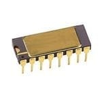
| 供应商器件封装 | 16-CDIP 侧面铜焊 |
| 共模抑制比—最小值 | 70 dB |
| 包装 | 管件 |
| 压摆率 | 5 V/µs |
| 双重电源电压 | +/- 9 V, +/- 12 V, +/- 15 V |
| 商标 | Analog Devices |
| 增益带宽生成 | 25 MHz |
| 增益带宽积 | 25MHz |
| 安装类型 | 通孔 |
| 安装风格 | Through Hole |
| 封装 | Tube |
| 封装/外壳 | 16-CDIP(0.300",7.62mm) |
| 封装/箱体 | CDIP |
| 工作温度 | -55°C ~ 125°C |
| 工厂包装数量 | 23 |
| 放大器类型 | Instrumentation Amplifier |
| 最大功率耗散 | 450 mW |
| 最大工作温度 | + 125 C |
| 最大输入电阻 | 1000 MOhms (Typ) |
| 最小工作温度 | - 55 C |
| 标准包装 | 1 |
| 电压-电源,单/双 (±) | ±6 V ~ 18 V |
| 电压-输入失调 | 50µV |
| 电流-电源 | 3.5mA |
| 电流-输入偏置 | 30nA |
| 电流-输出/通道 | - |
| 电路数 | 1 |
| 系列 | AD625 |
| 视频文件 | http://www.digikey.cn/classic/video.aspx?PlayerID=1364138032001&width=640&height=505&videoID=2245193153001http://www.digikey.cn/classic/video.aspx?PlayerID=1364138032001&width=640&height=505&videoID=2245193159001 |
| 输入补偿电压 | 0.05 mV |
| 输出类型 | - |
| 通道数量 | 1 Channel |


- 商务部:美国ITC正式对集成电路等产品启动337调查
- 曝三星4nm工艺存在良率问题 高通将骁龙8 Gen1或转产台积电
- 太阳诱电将投资9.5亿元在常州建新厂生产MLCC 预计2023年完工
- 英特尔发布欧洲新工厂建设计划 深化IDM 2.0 战略
- 台积电先进制程称霸业界 有大客户加持明年业绩稳了
- 达到5530亿美元!SIA预计今年全球半导体销售额将创下新高
- 英特尔拟将自动驾驶子公司Mobileye上市 估值或超500亿美元
- 三星加码芯片和SET,合并消费电子和移动部门,撤换高东真等 CEO
- 三星电子宣布重大人事变动 还合并消费电子和移动部门
- 海关总署:前11个月进口集成电路产品价值2.52万亿元 增长14.8%


PDF Datasheet 数据手册内容提取
a Programmable Gain Instrumentation Amplifier AD625 FEATURES FUNCTIONAL BLOCK DIAGRAM User Programmed Gains of 1 to 10,000 Low Gain Error: 0.02% Max Low Gain TC: 5 ppm/(cid:2)C Max 50(cid:1) AD625 Low Nonlinearity: 0.001% Max –INPUT – + – + Low Offset Voltage: 25 (cid:3)V –GAIN 10k(cid:1) Low Noise 4 nV/√Hz (at 1 kHz) RTI SENSE SENSE Gain Bandwidth Product: 25 MHz D–GRAIVINE 10k(cid:1) – 16-Lead Ceramic or Plastic DIP Package, VB 10k(cid:1) OUTPUT 20-Terminal LCC Package +GAIN + Standard Military Drawing Available DRIVE 10k(cid:1) +GAIN REFERENCE MlL-Standard Parts Available SENSE Low Cost 50(cid:1) + + +INPUT – – PRODUCT DESCRIPTION PRODUCT HIGHLIGHTS The AD625 is a precision instrumentation amplifier specifically 1. The AD625 affords up to 16-bit precision for user selected designed to fulfill two major areas of application: 1) Circuits re- fixed gains from 1 to 10,000. Any gain in this range can be quiring nonstandard gains (i.e., gains not easily achievable with programmed by 3 external resistors. devices such as the AD524 and AD624). 2) Circuits requiring a 2. A 12-bit software programmable gain amplifier can be config- low cost, precision software programmable gain amplifier. ured using the AD625, a CMOS multiplexer and a resistor For low noise, high CMRR, and low drift the AD625JN is the network. Unlike previous instrumentation amplifier designs, most cost effective instrumentation amplifier solution available. the ON resistance of a CMOS switch does not affect the gain An additional three resistors allow the user to set any gain from accuracy. 1 to 10,000. The error contribution of the AD625JN is less than 3. The gain accuracy and gain temperature coefficient of the 0.05% gain error and under 5 ppm/°C gain TC; performance amplifier circuit are primarily dependent on the user selected limitations are primarily determined by the external resistors. external resistors. Common-mode rejection is independent of the feedback resistor matching. 4. The AD625 provides totally independent input and output offset nulling terminals for high precision applications. This A software programmable gain amplifier (SPGA) can be config- minimizes the effects of offset voltage in gain-ranging ured with the addition of a CMOS multiplexer (or other switch applications. network), and a suitable resistor network. Because the ON resistance of the switches is removed from the signal path, an 5. The proprietary design of the AD625 provides input voltage AD625 based SPGA will deliver 12-bit precision, and can be noise of 4 nV/√Hz at 1 kHz. programmed for any set of gains between 1 and 10,000, with 6. External resistor matching is not required to maintain high completely user selected gain steps. common-mode rejection. For the highest precision the AD625C offers an input offset voltage drift of less than 0.25 µV/°C, output offset drift below 15 µV/°C, and a maximum nonlinearity of 0.001% at G = 1. All grades exhibit excellent ac performance; a 25 MHz gain band- width product, 5 V/µs slew rate and 15 µs settling time. The AD625 is available in three accuracy grades (A, B, C) for industrial (–40°C to +85°C) temperature range, two grades (J, K) for commercial (0°C to +70°C) temperature range, and one (S) grade rated over the extended (–55°C to +125°C) tempera- ture range. REV.D Information furnished by Analog Devices is believed to be accurate and reliable. However, no responsibility is assumed by Analog Devices for its One Technology Way, P.O. Box 9106, Norwood, MA 02062-9106, U.S.A. use, nor for any infringements of patents or other rights of third parties which may result from its use. No license is granted by implication or Tel: 781/329-4700 World Wide Web Site: http://www.analog.com otherwise under any patent or patent rights of Analog Devices. Fax: 781/326-8703 © Analog Devices, Inc., 2000
AD625–SPECIFICATIONS (typical @ V = (cid:4)15 V, R = 2 k(cid:1) and T = + 25(cid:2)C, unless otherwise noted) S L A AD625A/J/S AD625B/K AD625C Model Min Typ Max Min Typ Max Min Typ Max Unit GAIN 2R 2R 2R Gain Equation RF +1 RF +1 RF +1 G G G Gain Range 1 10,000 1 10,000 1 110,000 Gain Error1 ±.035 (cid:4)0.05 ±0.02 (cid:4)0.03 ±0.01 (cid:4)0.02 % Nonlinearity, Gain = 1-256 ±0.005 ±0.002 ±0.001 % Gain>256 ±0.01 ±0.008 ±0.005 % Gain vs. Temp. Gain<10001 5 5 5 ppm/°C GAIN SENSE INPUT Gain Sense Current 300 500 150 250 50 100 nA vs. Temperature 5 20 2 15 2 10 nA/°C Gain Sense Offset Current 150 500 75 250 50 100 nA vs. Temperature 2 15 1 10 2 10 nA/°C VOLTAGE OFFSET (May be Nulled) Input Offset Voltage 50 200 25 50 10 25 µV vs. Temperature 1 2/2 0.25 0.50/1 0.1 0.25 µV/°C Output Offset Voltage 4 5 2 3 1 2 mV vs. Temperature 20 50/50 10 25/40 10 15 µV/°C Offset Referred to the Input vs. Supply G = 1 70 75 75 85 80 90 dB G = 10 85 95 90 100 95 105 dB G = 100 95 100 105 110 110 120 dB G = 1000 100 110 110 120 115 140 dB INPUT CURRENT Input Bias Current ±30 (cid:4)50 ±20 (cid:4)25 ±10 (cid:4)15 nA vs. Temperature ±50 ±50 ±50 pA/°C Input Offset Current ±2 (cid:4)35 ±1 (cid:4)15 ±1 (cid:4)5 nA vs. Temperature ±20 ±20 ±20 pA/°C INPUT Input Impedance Differential Resistance 1 1 1 GΩ Differential Capacitance 4 4 4 pF Common-Mode Resistance 1 1 1 GΩ Common-Mode Capacitance 4 4 4 pF Input Voltage Range Differ. Input Linear (V )2 ±10 ±10 ±10 V DL ( ) ( ) ( ) Common-Mode Linear (V ) 12V – G ×V 12V – G ×V 12V – G ×V CM 2 D 2 D 2 D Common-Mode Rejection Ratio dc to 60 Hz with 1 kΩ Source Imbalance G = 1 70 75 75 85 80 90 dB G = 10 90 95 90 105 100 115 dB G = 100 100 105 105 115 110 125 dB G = 1000 110 115 110 125 120 140 dB OUTPUT RATING ±10 V ±10 V ±10 V @ 5 mA @ 5 mA @ 5 mA DYNAMIC RESPONSE Small Signal –3 dB G = 1 (R = 20 kΩ) 650 650 650 kHz F G = 10 400 400 400 kHz G = 100 150 150 150 kHz G = 1000 25 25 25 kHz Slew Rate 5.0 5.0 5.0 V/µs Settling Time to 0.01%, 20 V Step G = 1 to 200 15 15 15 µs G = 500 35 35 35 µs G = 1000 75 75 75 µs –2– REV. D
AD625 AD625A/J/S AD625B/K AD625C Model Min Typ Max Min Typ Max Min Typ Max Unit NOISE Voltage Noise, 1 kHz R.T.I. 4 4 4 nV/√Hz R.T.O. 75 75 75 nV/√Hz R.T.I., 0.1 Hz to 10 Hz G = 1 10 10 10 µV p-p G = 10 1.0 1.0 1.0 µV p-p G = 100 0.3 0.3 0.3 µV p-p G = 1000 0.2 0.2 0.2 µV p-p Current Noise 0.1 Hz to 10 Hz 60 60 60 pA p-p SENSE INPUT R 10 10 10 kΩ IN I 30 30 30 µA IN Voltage Range ±10 ±10 ±10 V Gain to Output 1 ± 0.01 1 ± 0.01 1 ± 0.01 % REFERENCE INPUT R 20 20 20 kΩ IN I 30 30 30 µA IN Voltage Range ±10 ±10 ±10 V Gain to Output 1 ± 0.01 1 ± 0.01 1 ± 0.01 % TEMPERATURE RANGE Specified Performance J/K Grades 0 +70 0 +70 °C A/B/C Grades –40 +85 –40 +85 –40 +85 °C S Grade –55 +125 °C Storage –65 +150 –65 +150 –65 +150 °C POWER SUPPLY Power Supply Range ±6 to ±18 ±6 to ±18 ±6 to ±18 V Quiescent Current 3.5 5 3.5 5 3.5 5 mA NOTES 1Gain Error and Gain TC are for the AD625 only. Resistor Network errors will add to the specified errors. 2V is the maximum differential input voltage at G = 1 for specified nonlinearity. V at other gains = 10 V/G. V = actual differential input voltage. DL DL D Example: G = 10, V = 0.50; V = 12 V – (10/2 × 0.50 V) = 9.5 V. D CM Specifications subject to change without notice. All min and max specifications are guaranteed. Specifications shown in boldface are tested on all production units at final electrical test. Results from those tests are used to calculate outgoing quality levels. REV. D –3–
AD625 ABSOLUTE MAXIMUM RATINGS* Operating Temperature Range SupplyVoltage . . . . . . . . . . . . . . . . . . . . . . . . . . . . . . . . .±18V AD625J/K . . . . . . . . . . . . . . . . . . . . . . . . . . . .0°C to +70°C InternalPowerDissipation . . . . . . . . . . . . . . . . . . . . . .450 mW AD625A/B/C . . . . . . . . . . . . . . . . . . . . . . . .–40°C to +85°C Input Voltage . . . . . . . . . . . . . . . . . . . . . . . . . . . . . . . . . . .±V AD625S . . . . . . . . . . . . . . . . . . . . . . . . . . .–55°C to +125°C S DifferentialInputVoltage . . . . . . . . . . . . . . . . . . . . . . . . .±V Lead Temperature Range (Soldering10sec) . . . . . . . . +300°C S Output Short Circuit Duration . . . . . . . . . . . . . . . . Indefinite *Stresses above those listed under Absolute Maximum Ratings may cause perma- Storage Temperature Range (D, E) . . . . . . . .–65°C to +150°C nent damage to the device. This is a stress rating only; functional operation of the Storage Temperature Range (N) . . . . . . . . . .–65°C to +125°C device at these or any other conditions above those indicated in the operational section of this specification is not implied. Exposure to absolute maximum rating conditions for extended periods may affect device reliability. ORDERING GUIDE Model Temperature Range Package Description Package Option AD625AD –40°C to +85°C 16-Lead Ceramic DIP D-16 AD625BD –40°C to +85°C 16-Lead Ceramic DIP D-16 AD625BD/+ –40°C to +85°C 16-Lead Ceramic DIP D-16 AD625CD –40°C to +85°C 16-Lead Ceramic DIP D-16 AD625SD –55°C to +125°C 16-Lead Ceramic DIP D-16 AD625SD/883B –55°C to +125°C 16-Lead Ceramic DIP D-16 AD625SE/883B –55°C to +125°C 20-Terminal Leadless Chip Carrier E-20A AD625JN 0°C to +70°C 16-Lead Plastic DIP N-16 AD625KN 0°C to +70°C 16-Lead Plastic DIP N-16 AD625ACHIPS –40°C to +85°C Die AD625SCHIPS –55°C to +125°C Die 5962-87719012A* –55°C to +125°C 20-Terminal Leadless Chip Carrier E-20A 5962-8771901EA* –55°C to +125°C 16-Lead Ceramic DIP D-16 *Standard Military Drawing Available CAUTION ESD (electrostatic discharge) sensitive device. Electrostatic charges as high as 4000 V readily WARNING! accumulate on the human body and test equipment and can discharge without detection. Although the AD625 features proprietary ESD protection circuitry, permanent damage may occur on devices subjected to high-energy electrostatic discharges. Therefore, proper ESD ESD SENSITIVE DEVICE precautions are recommended to avoid performance degradation or loss of functionality. PIN CONNECTIONS Ceramic DIP (D) and Plastic DIP (N) Packages Leadless Chip Carrier (E) Package +INPUT 1 16 –INPUT SE SE N N E E +GAIN SENSE 2 15 –GAIN SENSE N S UT UT N S +VS RTI1 N0kU(cid:1)LL 3 14 R1T0Ok(cid:1) NULL–VS +GAI3 +INP2 NC1 2–INP0 1–GAI9 4 AD625 13 RTI NULL RTO NULL TOP VIEW +GAIN DRIVE 5 (Not to Scale)12 –GAIN DRIVE RTI NULL4 18 RTO NULL NC 6 11 SENSE RTI NULL5 AD625 17 RTO NULL NC6 TOP VIEW 16 NC REFERENCE 7 10 VOUT +GAIN DRIVE7 (Not to Scale) 15 –GAIN NULL –VS 8 9 +VS NC8 14 SENSE NC = NO CONNECT 9 10 1112 13 RENCE–VS NC +VS VOUT E F E R NC = NO CONNECT –4– REV. D
Typical Performance Characteristics–AD625 20 20 30 (cid:4)ANGE – V 15 (cid:4)SWING – V 15 WING – V p-p 20 GE R 10 AGE 10 GE S A T A UT VOLT 5 25(cid:2)C PUT VOL 5 UT VOLT 10 P T P IN OU OUT 0 0 0 0 5 10 15 20 0 5 10 15 20 10 100 1k 10k SUPPLY VOLTAGE – (cid:4)V SUPPLY VOLTAGE – (cid:4)V LOAD RESISTANCE – (cid:1) Figure 1.Input Voltage Range vs. Figure 2.Output Voltage Swing Figure 3.Output Voltage Swing Supply Voltage, G = 1 vs. Supply Voltage vs. Load Resistance –160 30 –140 G = 1000 p-p –120 G = 100 – V G = 1, 100 1000 MRR – dM–1–0800 GG == 110 R RESPONSE 20 G = 500 BALNIMDIWTEIDDTH GAIN 100 C –60 WE 10 10 O P –40 L G = 100 UL 1 –20 F G = 1000 0 0 0 10 100 1k 10k 100k 10M 1k 10k 100k 1M 100 1k 10k 100k 1M 10M FREQUENCY – Hz FREQUENCY – Hz FREQUENCY – Hz Figure 4.CMRR vs. Frequency Figure 5.Large Signal Frequency Figure 6.Gain vs. Frequency RTI, Zero to 1 kΩ Source Imbal- Response ance –1 160 160 (cid:5)(cid:3)V FROM FINAL VALUE – VOS 0123456 POWER SUPPLY REJECTION – dB11142086420000000 GGG === 5110000 1V– VpS-p = S –I1N5EVW dAcV+E POWER SUPPLY REJECTION – dB11142086420000000 GGG === 5110000 1V+ VpS-p = S +I1N5EVW dAcV+E 7 0 0 0 1.0 2.0 3.0 4.0 5.0 6.0 7.0 8.0 10 100 1k 10k 100k 10 100 1k 10k 100k WARM-UP TIME – Minutes FREQUENCY – Hz FREQUENCY – Hz Figure 7.Offset Voltage, RTI, Turn Figure 8.Negative PSRR vs. Figure 9.Positive PSRR vs. On Drift Frequency Frequency REV. D –5–
AD625 40 30 +VS A 20 n – T 10 N RRE 0 10V AD625 VOUT U C T –10 U P IN –20 –30 –VS –40 –125 –75 –25 25 75 125 TEMPERATURE – (cid:2)C Figure 10.Input Bias Current vs. Figure 11.Overrange and Gain Figure 12.Gain Overrange Recovery Temperature Switching Test Circuit (G = 8, G = 1) 8.0 Hz100k (cid:3)A A/ QUIESCENT CURRENT – 64..00 OLT NSD – nV/ Hz101010000 G = GG10 ==0 ,11 10000 E SPECTRAL DENSITY – f 110kk ER 2.0 V G = 1000 OIS 100 FI 1 N LI T P N M E A R 0 0.1 UR 10 0 5 10 15 20 1 10 100 1k 10k 100k C 1 10 100 1k 10k 100k SUPPLY VOLTAGE – (cid:4)V FREQUENCY – Hz FREQUENCY – Hz Figure 13.Quiescent Current vs. Figure 14.RTI Noise Spectral Figure 15.Input Current Noise Supply Voltage Density vs. Gain +VS –VS AD625 DUT 16.2k(cid:1) 1(cid:3)F +VS 1(cid:3)F AD712 1/2 1/2 AD712 9.09k(cid:1) 1(cid:3)F 16.2k(cid:1) G = 1, 10, 100 –VS G = 1000 1.62M(cid:1) 100(cid:1) 1k(cid:1) 1.82k(cid:1) Figure 16.Low Frequency Voltage Figure 17.Noise Test Circuit Figure 18.Low Frequency Voltage Noise, G = 1 (System Gain = 1000) Noise, G = 1000 (System Gain = 100,000) –6– REV. D
AD625 –12 TO 12 –8 TO 8 G = 1 G = 1000 G = 100 –4 TO 4 OUTPUT STEP – V 4 TO –4 G = 100 G = 1000 8 TO –8 G = 1 12 TO –12 0 10 20 30 40 50 60 70 Figure 19.Large Signal Pulse SETTLING TIME – (cid:3)S Figure 21.Large Signal Pulse Response and Settling Time, G = 1 Figure 20.Settling Time to 0.01% Response and Settling Time, G = 100 10k(cid:1) 1k(cid:1) 10k(cid:1) 1% 10T 1% 2I0NVP Up-Tp 100.01k%(cid:1) +VS VOUT AD625 1k(cid:1) 500(cid:1) 200(cid:1) 0.1% 0.1% 0.1% –VS Figure 22.Large Signal Pulse Figure 23.Settling Time Test Circuit Figure 24.Large Signal Pulse Response and Settling Time, G = 10 Response and Settling Time, G = 1000 REV. D –7–
AD625 THEORY OF OPERATION The diodes to the supplies are only necessary if input voltages The AD625 is a monolithic instrumentation amplifier based on outside of the range of the supplies are encountered. In higher a modification of the classic three-op-amp approach. Monolithic gain applications where differential voltages are small, back-to- construction and laser-wafer-trimming allow the tight matching back Zener diodes and smaller resistors, as shown in Figure and tracking of circuit components. This insures the high level 26b, provides adequate protection. Figure 26c shows low cost of performance inherent in this circuit architecture. FETs with a maximum ON resistance of 300 Ω configured to offer input protection with minimal degradation to noise, (5.2 nV/√Hz A preamp section (Q1–Q4) provides additional gain to A1 and compared to normal noise performance of 4 nV/√Hz). A2. Feedback from the outputs of A1 and A2 forces the collec- tor currents of Q1–Q4 to be constant, thereby, impressing the During differential overload conditions, excess current will flow input voltage across R . This creates a differential voltage at the through the gain sense lines (Pins 2 and 15). This will have no G outputs of A1 and A2 which is given by the gain (2R /R + 1) effect in fixed gain applications. However, if the AD625 is being F G times the differential portion of the input voltage. The unity used in an SPGA application with a CMOS multiplexer, this gain subtracter, A3, removes any common-mode signal from the current should be taken into consideration. The current capa- output voltage yielding a single ended output, V , referred to bilities of the multiplexer may be the limiting factor in allowable OUT the potential at the reference pin. overflow current. The ON resistance of the switch should be included as part of R when calculating the necessary input The value of R is the determining factor of the transconduc- G G protection resistance. tance of the input preamp stage. As R is reduced for larger G gains the transconductance increases. This has three important advantages. First, this approach allows the circuit to achieve a +VS very high open-loop gain of (3 × 10⁸ at programmed gains ≥ 500) 1.4k(cid:1) FD333 FD333 thus reducing gain related errors. Second, the gain-bandwidth +IN product, which is determined by C3, C4, and the input trans- RF conductance, increases with gain, thereby, optimizing frequency RG AD625 VOUT response. Third, the input voltage noise is reduced to a value RF determined by the collector current of the input transistors 1.4k(cid:1) (4 nV/√Hz). –IN FD333 FD333 INPUT PROTECTION –VS Differential input amplifiers frequently encounter input voltages Figure 26a.Input Protection Circuit outside of their linear range of operation. There are two consid- erations when applying input protection for the AD625; 1) that +VS continuous input current must be limited to less than 10 mA and 2) that input voltages must not exceed either supply by more than one diode drop (approximately 0.6 V @ 25°C). 500(cid:1) FD333 FD333 +IN Under differential overload conditions there is (R + 100) Ω in G 1N5837A RF series with two diode drops (approximately 1.2 V) between the RG AD625 VOUT plus and minus inputs, in either direction. With no external protec- 1N5837A tion and R very small (i.e., 40 Ω), the maximum overload RF G 500(cid:1) voltage the AD625 can withstand, continuously, is approximately –IN ±2.5 V. Figure 26a shows the external components necessary to FD333 protect the AD625 under all overload conditions at any gain. FD333 –VS +VS Figure 26b.Input Protection Circuit for G > 5 + 50(cid:3)A –VB 50(cid:3)A +VS FD333 A1 A2 10k(cid:1) FD333 C3 C4 SENSE +IN 10k(cid:1) 2k(cid:1) VO 2N5952 RF DGRAIVINE GDRAIIVNE 10k(cid:1) 10k(cid:1) RG AD625 VOUT –IN 50(cid:1) Q1, Q3 RFRGRF Q2, Q4 50(cid:1) +IN REF –IN 2k(cid:1) FDR3F33 GAIN GAIN 2N5952 SENSE SENSE 50(cid:3)A 50(cid:3)A FD333 –VS –VS Figure 26c.Input Protection Circuit Figure 25.Simplified Circuit of the AD625 –8– REV. D
AD625 Any resistors in series with the inputs of the AD625 will degrade RTO NOISE RTO OFFSET VOLTAGE tsthhheao nun lo5di, s beeei tp hueesrref odtrh imef atchnirecc egu.ai tFi nionsr aFtrhiegi sua lrrlee g a2rse6oaant eotrhr etihn ca iFnrci g5uu.i trF eino 2r F6 gciag icunarsne l e2bs6esb – nV Hz300 ACTOR3 used. The two 1.4 kΩ resistors in Figure 26a will degrade the SE G F OI200 N noise performance to: N YI 4kTRext+(4nV/ Hz)2 =7.9nV/ Hz VOLTAGE 100 MULTIPL2 10k 20k 30k 40k 50k 60k 10k 20k 30k 40k 50k 60k RESISTOR PROGRAMMABLE GAIN AMPLIFIER FEEDBACK RESISTANCE – (cid:1) FEEDBACK RESISTANCE – (cid:1) In the resistor-programmed mode (Figure 27), only three exter- RTO OFFSET VOLTAGE DRIFT BANDWIDTH nal resistors are needed to select any gain from 1 to 10,000. 6 1M 10k(cid:1) Depending on the application, discrete components or a R pTA5co rDCpempt 6ramm2irm5eo/° CmnpC- rem cigdmoao nnaidntreeri til Twbyv uoCodltr.teek atsT ge clrehaem,esn smi g nbtaaeheikd naui n nbss geey0 dn .tt0.shh e2eTe %c hCeue xMrt trogeeR argninRnata i inlaos c r feie cntrsuhrsiroseeatnr ocr saeryinsst aiidsvsnit enuod ctrn og edpa etrihnore- ULTIPLYING FACTO 5432 FREQUENCY – Hz10100kk 20k(cid:1) 50k(cid:1) M grammed AD625 independent of the match of the two feedback 1 resistors, RF. 10k 20k 30k 40k 50k 60k 1 10 100 1k FEEDBACK RESISTANCE – (cid:1) FEEDBACK RESISTANCE – (cid:1) Selecting Resistor Values As previously stated each R provides feedback to the input Figure 28.RTO Noise, Offset, Drift and Bandwidth vs. F stage and sets the unity gain transconductance. These feedback Feedback Resistance Normalized to 20 kΩ resistors are provided by the user. The AD625 is tested and specified with a value of 20 kΩ for R . Since the magnitude of Table I. Common Gains Nominally Within (cid:4)0.5% Error F RTO errors increases with increasing feedback resistance, values Using Standard 1% Resistors much above 20 kΩ are not recommended (values below 10 kΩ GAIN R R for R may lead to instability). Refer to the graph of RTO noise, F G F offset, drift, and bandwidth (Figure 28) when selecting the 1 20 kΩ ∞ feedback resistors. The gain resistor (R ) is determined by the 2 19.6 kΩ 39.2 kΩ G formula R = 2 R /(G – l). 5 20 kΩ 10 kΩ G F 10 20 kΩ 4.42 kΩ G = 2 R F +1 20 20 kΩ 2.1 kΩ RG 50 19.6 kΩ 806 Ω RF +INPUT RG –INPUT RF 100 20 kΩ 402 Ω 200 20.5 kΩ 205 Ω 1 16 500 19.6 kΩ 78.7 Ω +GAIN –GAIN SENSE 2 15 SENSE 1000 19.6 kΩ 39.2 Ω RTI NULL RTO 4 20 kΩ 13.3 kΩ +VRSTI NULL 34 1143 NRNUTUOLLLL 186 1290. k6Ω kΩ 52..6627 kkΩΩ 5 A1 A2 12 32 19.6 kΩ 1.27 kΩ +GAIN DRIVE –GAIN DRIVE NC 6 11 64 20 kΩ 634 Ω REF 10k(cid:1) 10k(cid:1) VOUT 128 20 kΩ 316 Ω 7 10 10k(cid:1) A3 10k(cid:1) 256 19.6 kΩ 154 Ω –VS 8 AD625 9 +VS 512 19.6 kΩ 76.8 Ω 1024 19.6 kΩ 38.3 Ω Figure 27.AD625 in Fixed Gain Configuration A list of standard resistors which can be used to set some com- SENSE TERMINAL mon gains is shown in Table I. The sense terminal is the feedback point for the AD625 output For single gain applications, only one offset null adjust is neces- amplifier. Normally it is connected directly to the output. If sary; in these cases the RTI null should be used. heavy load currents are to be drawn through long leads, voltage drops through lead resistance can cause errors. In these in- stances the sense terminal can be wired to the load thus putting REV. D –9–
AD625 the I × R drops “inside the loop” and virtually eliminating this GNDVDDVSS error source. Typically, IC instrumentation amplifiers are rated for a full ±10 volt output swing into 2 kΩ. In some applications, however, the A0 +IN +VS need exists to drive more current into heavier loads. Figure 29 A1 shows how a high-current booster may be connected “inside the EN SENSE loop” of an instrumentation amplifier. By using an external AD7502 power boosting circuit, the power dissipated by the AD625 will AD625 VOUT remain low, thereby, minimizing the errors induced by self- heating. The effects of nonlinearities, offset and gain inaccura- cies of the buffer are reduced by the loop gain of the AD625’s output amplifier. –VS REFERENCE –IN +VS VS39k(cid:1) VREF VIN+ SENSE AD589 1.2V +VS 0.01(cid:3)F RRGF AD625 X1 DATAMSB RFBC1 +VS 20kR(cid:1)3 2Rk5(cid:1) INPUTS RF RI LSB AD7524 OUT 1 1/2 VIN– REFERENCE CS 8-BIT DAC OUT 2 AD712 10Rk4(cid:1) 1/2 AD712 –VS WR 5k(cid:1) Figure 29.AD625 /Instrumentation Amplifier with Output –VS Current Booster Figure 30.Software Controllable Offset REFERENCE TERMINAL The reference terminal may be used to offset the output by up An instrumentation amplifier can be turned into a voltage-to- to ±10 V. This is useful when the load is “floating” or does not current converter by taking advantage of the sense and reference share a ground with the rest of the system. It also provides a terminals as shown in Figure 31. direct means of injecting a precise offset. However, it must be remembered that the total output swing is ±10 volts, from VIN+ SENSE ground, to be shared between signal and reference offset. RF Tzehroe AimDp6e2d5a nrceefe. rAenncye s tigernmifiicnaanl tm reussits tbaen cper,e sinencltuedd iwngit hth noesearly RG AD625 +RV1X– caused by PC layouts or other connection techniques, will in- RF IL crease the gain of the noninverting signal path, thereby, upset- VIN– AD711 ting the common-mode rejection of the in-amp. Inadvertent thermocouple connections created in the sense and reference LOAD lines should also be avoided as they will directly affect the out- put offset voltage and output offset voltage drift. Figure 31.Voltage-to-Current Converter In the AD625 a reference source resistance will unbalance the By establishing a reference at the “low” side of a current setting CMR trim by the ratio of 10 kΩ/R . For example, if the refer- REF resistor, an output current may be defined as a function of input ence source impedance is 1 Ω, CMR will be reduced to 80 dB voltage, gain and the value of that resistor. Since only a small (10 kΩ/1 Ω = 80 dB). An operational amplifier may be used to current is demanded at the input of the buffer amplifier A1, the provide the low impedance reference point as shown in Figure forced current I will largely flow through the load. Offset and 30. The input offset voltage characteristics of that amplifier will L drift specifications of A2 must be added to the output offset and add directly to the output offset voltage performance of the drift specifications of the In-Amp. instrumentation amplifier. The circuit of Figure 30 also shows a CMOS DAC operating in INPUT AND OUTPUT OFFSET VOLTAGE the bipolar mode and connected to the reference terminal to Offset voltage specifications are often considered a figure of provide software controllable offset adjustments. The total offset merit for instrumentation amplifiers. While initial offset may be range is equal to ±(VREF/2 × R5/R4), however, to be symmetri- adjusted to zero, shifts in offset voltage due to temperature cal about 0 V R3 = 2 × R4. variations will cause errors. Intelligent systems can often correct The offset per bit is equal to the total offset range divided by 2N, for this factor with an autozero cycle, but this requires extra where N = number of bits of the DAC. The range of offset for circuitry. Figure 30 is ±120 mV, and the offset is incremented in steps of 0.9375 mV/LSB. –10– REV. D
AD625 Offset voltage and offset voltage drift each have two compo- in distributed stray capacitances. In many applications shielded nents: input and output. Input offset is that component of offset cables are used to minimize noise. This technique can create that is generated at the input stage. Measured at the output it is directly proportional to gain, i.e., input offset as measured at the +VS output at G = 100 is 100 times greater than that measured at +INPUT G = 1. Output offset is generated at the output and is constant SENSE for all gains. 100(cid:1) AD711 RRGF AD625 VOUT The input offset and drift are multiplied by the gain, while the output terms are independent of gain, therefore, input errors RF dominate at high gains and output errors dominate at low gains. –INPUT REFERENCE The output offset voltage (and drift) is normally specified at –VS G = 1 (where input effects are insignificant), while input offset Figure 32.Common-Mode Shield Driver (and drift) is given at a high gain (where output effects are negli- common-mode rejection errors unless the shield is properly gible). All input-related parameters are specified referred to the driven. Figures 32 and 33 show active data guards which are input (RTI) which is to say that the effect on the output is “G” configured to improve ac common-mode rejection by “boot- times larger. Offset voltage vs. power supply is also specified as strapping” the capacitances of the input cabling, thus minimiz- an RTI error. ing differential phase shift. By separating these errors, one can evaluate the total error inde- pendent of the gain. For a given gain, both errors can be com- +INPUT bined to give a total error referred to the input (RTI) or output +VS AD712 (RTO) by the following formula: 100(cid:1) SENSE Total Error RTI = input error + (output error/gain) RF Total Error RTO = (Gain × input error) + output error RG AD625 VOUT The AD625 provides for both input and output offset voltage 100(cid:1) –VS RF REFERENCE adjustment. This simplifies nulling in very high precision appli- –INPUT cations and minimizes offset voltage effects in switched gain –VS applications. In such applications the input offset is adjusted Figure 33.Differential Shield Driver first at the highest programmed gain, then the output offset is adjusted at G = 1. If only a single null is desired, the input offset GROUNDING null should be used. The most additional drift when using only In order to isolate low level analog signals from a noisy digital the input offset null is 0.9 µV/°C, RTO. environment, many data-acquisition components have two or more ground pins. These grounds must eventually be tied to- COMMON-MODE REJECTION gether at one point. It would be convenient to use a single Common-mode rejection is a measure of the change in output ground line, however, current through ground wires and pc runs voltage when both inputs are changed by equal amounts. These of the circuit card can cause hundreds of millivolts of error. specifications are usually given for a full-range input voltage Therefore, separate ground returns should be provided to mini- change and a specified source imbalance. mize the current flow from the sensitive points to the system ground (see Figure 34). Since the AD625 output voltage is In an instrumentation amplifier, degradation of common-mode developed with respect to the potential on the reference termi- rejection is caused by a differential phase shift due to differences nal, it can solve many grounding problems. STATUS ANALOG AD7502 AD583 OUT INPUT AD625 SAMPLE AD574A SIGNAL AND HOLD A/D CONVERTER HOLD +VS CAP –VS –VS +VS VLOGIC +VS –VS +VS–VS DIGITAL COMMON ANALOG POWER GROUND Figure 34.Basic Grounding Practice for a Data Acquisition System REV. D –11–
AD625 GROUND RETURNS FOR BIAS CURRENTS high thermoelectric potential (about 35 µV°C). This means that Input bias currents are those currents necessary to bias the input care must be taken to insure that all connections (especially transistors of a dc amplifier. There must be a direct return path those in the input circuit of the AD625) remain isothermal. This for these currents, otherwise they will charge external capaci- includes the input leads (1, 16) and the gain sense lines (2, 15). tances, causing the output to drift uncontrollably or saturate. These pins were chosen for symmetry, helping to desensitize the Therefore, when amplifying “floating” input sources such as input circuit to thermal gradients. In addition, the user should transformers, or ac-coupled sources, there must be a dc path also avoid air currents over the circuitry since slowly fluctuating from each input to ground as shown in Figure 35. GNDVDDVSS +VS SENSE RF RG AD625 VOUT +VS 15 16 RF LOAD AD7502 –VS REFERENCE TOSU PPOPWLEYR 14 AD625 910 VOUT GROUND + 0.1(cid:3)F LOW VIN 13 LEAKAGE – Figure 35a.Ground Returns for Bias Currents with 1k(cid:1) 11 Transformer Coupled Inputs –VS AD711 12 +VS SENSE RF RG AD625 VOUT VDD VSS AD7510DIKD RF LOAD GND REFERENCE TO POWER 200(cid:3)s –VS SUPPLY ZERO PULSE A1 A2 A3 A4 GROUND Figure 36. Auto-Zero Circuit Figure 35b.Ground Returns for Bias Currents with thermocouple voltages will appear as “flicker” noise. In SPGA Thermocouple Input applications relay contacts and CMOS mux leads are both potential sources of additional thermocouple errors. +VS The base emitter junction of an input transistor can rectify out SENSE of band signals (i.e., RF interference). When amplifying small RF signals, these rectified voltages act as small dc offset errors. The RG AD625 VOUT AD625 allows direct access to the input transistors’ bases and RF LOAD emitters enabling the user to apply some first order filtering to these unwanted signals. In Figure 37, the RC time constant REFERENCE TO POWER should be chosen for desired attenuation of the interfering signals. 100k(cid:1) 100k(cid:1) –VS SUPPLY GROUND In the case of a resistive transducer, the capacitance alone work- ing against the internal resistance of the transducer may suffice. Figure 35c.Ground Returns for Bias Currents with AC Coupled Inputs RF RG RF R R AUTOZERO CIRCUITS FILTER +IN –IN FILTER CAP CAP In many applications it is necessary to maintain high accuracy. C C At room temperature, offset effects can be nulled by the use of 1 16 +IN –IN offset trimpots. Over the operating temperature range, however, +GAIN SENSE –GAIN SENSE 2 15 offset nulling becomes a problem. For these applications the RTI NULL RTO autozero circuit of Figure 36 provides a hardware solution. +V 3 14 NULL RTO 4 13 RTI NULL NULL OTHER CONSIDERATIONS 5 A1 A2 12 +GAIN DRIVE –GAIN DRIVE One of the more overlooked problems in designing ultralow- SENSE NC 6 11 drift dc amplifiers is thermocouple induced offset. In a circuit REF 10k(cid:1) 10k(cid:1) VOUT 7 10 comprised of two dissimilar conductors (i.e., copper, kovar), a 10k(cid:1) 10k(cid:1) VOUT A3 current flows when the two junctions are at different tempera- –VS 8 AD625 9 +VS tures. When this circuit is broken, a voltage known as the “Seebeck” or thermocouple emf can be measured. Standard IC Figure 37.Circuit to Attenuate RF Interference lead material (kovar) and copper form a thermocouple with a –12– REV. D
AD625 These capacitances may also be incorporated as part of the external input protection circuit (see section on Input Protec- –INPUT AD625 –GAIN tion). As a general practice every effort should be made to SENSE match the extraneous capacitance at Pins 15 and 2, and Pins 1 20k(cid:1) –GAIN and 16, to preserve high ac CMR. CS-OUT 15.6k(cid:1) DRIVE SOFTWARE PROGRAMMABLE GAIN AMPLIFIER RON 3.9k(cid:1) 10k(cid:1) 10k(cid:1) An SPGA provides the ability to externally program precision – COUT IOUT IS CS 975k(cid:1) 12-BIT gains from digital inputs. Historically, the problem in systems VIN CS-OUT 650k(cid:1) VS DAS + requiring electronic switching of gains has been the ON resis- RON 975k(cid:1) 10k(cid:1) tance (RON) of the multiplexer, which appears in series with the COUT IOUT IS CS 3.9k(cid:1) +GAIN 10k(cid:1) gain setting resistor RG. This can result in substantial gain errors 15.6k(cid:1) DRIVE and gain drifts. The AD625 eliminates this problem by making 20k(cid:1) +GAIN the gain drive and gain sense pins available (Pins 2, 15, 5, 12; SENSE see Figure 39). Consequently the multiplexer’s ON resistance is +INPUT removed from the signal current path. This transforms the ON resistance error into a small nullable offset error. To clarify this Figure 39.SPGA with Multiplexer Error Sources point, an error budget analysis has been performed in Table II Figure 39 shows a complete SPGA feeding a 12-bit DAS with a based on the SPGA configuration shown in Figure 39. 0 V–10 V input range. This configuration was used in the error budget analysis shown in Table II. The gain used for the RTI AD7502 calculations is set at 16. As the gain is changed, the ON resis- TTL/DTL TO CMOS LEVEL TRANSLATOR VSS A0 tance of the multiplexer and the feedback resistance will change, VDD DECODER/DRIVER A1 which will slightly alter the values in the table. GND EN Table II. Errors Induced by Multiplexer to an SPGA 3.9k(cid:1) 975(cid:1) 650(cid:1) 975(cid:1) 3.9k(cid:1) Induced Specifications Voltage Offset 20k(cid:1) 15.6k(cid:1) 15.6k(cid:1) 20k(cid:1) Error AD625C AD7520KN Calculation Induced RTI RTI Offset Gain Sense Switch 40 nA × 170 Ω = 6.8 µV +INPUT –INPUT Voltage Offset Resistance 6.8 µV Current 170 Ω 40 nA 1 16 +GAIN –GAIN SENSE 2 15 SENSE RTI Offset Gain Sense Differential 60 nA × 6.8 Ω = 0.41 µV Voltage Current Switch 0.41 µV RTI NULL RTO NULL 3 14 60 nA Resistance +VS –VS 6.8 Ω 4 13 RTI NULL RTO NULL 5 A1 A2 12 RTO Offset Feedback Differential 2 (0.2 nA × 20 kΩ) 0.5 µV +GAIN DRIVE –GAIN DRIVE Voltage Resistance Leakage = 8 µV/16 RNECF 67 10k(cid:1) 10k(cid:1) 1110 VOUT 20 kΩ1 C+0u.r2re nnAt (IS)2 10k(cid:1) A3 10k(cid:1) –0.2 nA –VS 8 AD625 9 +VS RTO Offset Feedback Differential 2 (1 nA × 20 kΩ) 2.5 µV Voltage Resistance Leakage = 40 µV/16 Figure 38. SPGA in a Gain of 16 20 kΩ1 Current (I )2 Figure 38 shows an AD625 based SPGA with possible gains of OUT +1 nA 1, 4, 16, 64. RG equals the resistance between the gain sense –1 nA lines (Pins 2 and 15) of the AD625. In Figure 38, R equals the sum of the two 975 Ω resistors and the 650 Ω resGistor, or Total error induced by a typical CMOS multiplexer to an SPGA at +25°C 10.21 (cid:3)A 2600 Ω. R equals the resistance between the gain sense and the F gain drive pins (Pins 12 and 15, or Pins 2 and 5), that is R NOTES equals the 15.6 kΩ resistor plus the 3.9 kΩ resistor, or 19.5F kΩ. 1The resistor for this calculation is the user-provided feedback resistance (RF). 20 kΩ is recommended value (see Resistor Programmable Gain Amplifier section). The gain, therefore equals: 2The leakage currents (I and I ) will induce an offset voltage, however, the offset S OUT will be determined by the difference between the leakages of each “half’’ of the 2R 2(19.5kΩ) differential multiplexer. The differential leakage current is multiplied by the F +1= +1=16 feedback resistance (see Note 1), to determine offset voltage. Because differential R (2.6kΩ) leakage current is not a parameter specified on multiplexer data sheets, the most G extreme difference (one most positive and one most negative) was used for the As the switches of the differential multiplexer proceed synchro- calculations in Table II. Typical performance will be much better. nously, R and R change, resulting in the various programmed **The frequency response and settling will be affected by the ON resistance and G F internal capacitance of the multiplexer. Figure 40 shows the settling time vs. gain settings. ON resistance at different gain settings for an AD625 based SPGA. **Switch resistance and leakage current errors can be reduced by using relays. REV. D –13–
AD625 1800000 3) Begin all calculations with G0 = 1 and RF0 = 0. R = (20 kΩ – R ) (1–1/4): R = 0 ∴ R = 15 kΩ 400 F1 F0 F0 F1 RON = 1k(cid:1) R = [20 kΩ – (R + R )] (1–4/16): 200 F2 F0 F1 (cid:3)s100 RF0 + RF1 = 15 kΩ ∴ RF2 = 3.75 kΩ ME – 80 RON = 500(cid:1) RF3 = [20 kΩ – (RF0 + RF1 + RF2)] (1–16/64): SETTLING TI 4218000 RON = 0R(cid:1)ON = 200(cid:1) 4) Tmhine ecdeR nlaFts0e tr+. r IRetssFi 1sv ta+olur eR( RFis2G t =oh fe1 t8rhe.e7m 5ha ikignΩhine ∴sgt rgReasFii3ns t= as en9tc3tei7n o.g5f) ,tΩ hise d4e0t ekrΩ- string, and can be calculated with the equation: 4 2 R = (40 kΩ – 2∑M R ) G Fj 1 1 4 16 64 256 1024 4096 j=0 GAIN RG = 40 kΩ – 2 (RF0 + RF1 + RF2 + RF3) Figure 40.Time to 0.01% of a 20 V Step Input for 40 kΩ – 39.375 kΩ = 625 Ω SPGA with AD625 5) If different resistor values are desired, all the resistors in the network can be scaled by some convenient factor. However, DETERMINING SPGA RESISTOR NETWORK VALUES raising the impedance will increase the RTO errors, lowering The individual resistors in the gain network can be calculated the total network resistance below 20 kΩ can result in ampli- sequentially using the formula given below. The equation deter- fier instability. More information on this phenomenon is mines the resistors as labeled in Figure 41. The feedback resis- given in the RPGA section of the data sheet. The scale factor tors and the gain setting resistors are interactive, therefore; the will not affect the unity gain feedback resistors. The resistor formula must be a series where the present term is dependent on network in Figure 38 has a scaling factor of 650/625 = 1.04, the preceding term(s). The formula if this factor is used on R , R , R , and R , then the resis- F1 F2 F3 G tor values will match exactly. R = (20 kΩ – ∑1 R )(1– Gi ) G0 =1 Fi+1 j=0 Fj Gi=1 RF0 = 0 6) Rcaoruryn das o mff aenryro srisg ncaifnic bane tc duimgiutsl aatsiv peo, stshiebrleef ournet,i li ta lils tahdev ivsaeldu etso can be used to calculate the necessary feedback resistors for any have been calculated. set of gains. This formula yields a network with a total resistance of 40 kΩ. A dummy variable (j) serves as a counter to keep a AD75xx running total of the preceding feedback resistors. To illustrate how the formula can be applied, an example similar to the calculation used for the resistor network in Figure 38 is exam- ined below. TO GAIN SENSE TO GAIN SENSE (PIN 2) RF2 RFN RFG RFN RF2 (PIN 15) 1) Unity gain is treated as a separate case. It is implemented 20k(cid:1) RF1 20k(cid:1) with separate 20 kΩ feedback resistors as shown in Figure 41. CONNECT IF UNITY CONNECT IF UNITY It is then ignored in further calculations. GAIN IS DESIRED GAIN IS DESIRED TO GAIN DRIVE TO GAIN DRIVE 2) Before making any calculations it is advised to draw a resistor (PIN 5) (PIN 12) network similar to the network in Figure 41. The network Figure 41.Resistors for a Gain Setting Network will have (2 × M) + 1 resistors, where M = number of gains. For Figure 38 M = 3 (4, 16, 64), therefore, the resistor string will have seven resistors (plus the two 20 kΩ “side” resistors for unity gain). –14– REV. D
AD625 OUTLINE DIMENSIONS Dimensions shown in inches and (mm). 16-Lead Plastic DIP (N-16) 16-Lead Ceramic DIP (D-16) 0.755 (19.18) 0.430 D) 0.745 (18.93) (10.922) v. 0.040R 16 9 e 161 89 00.2.264 ( (66.6.11)) 70.8.37140 (cid:4) (cid:4)00..20514) 0(6.2.7635) (07.2.3970 (cid:4)(cid:4)00..205140) 00 (r 0.306 (7.78) 1 8 6/ PIN 1 0.294 (7.47) 0– PIN 1 – 0.17 (4M.3A2X) 00..1142 ((33..5065)) 200.8.3020 (cid:4)(cid:4)00..201540 0.035 (cid:4)0.01 (0R7.3.E60F20) 0780c 00.1.1725 ((34..0455)) SPELAANTIENG 0.012 (0.305) 0.095 (2.41) (0.889 (cid:4)0.254) 0.085 (2.159) C0 00.0.0125 ((00.5.30881)) 00..001955 ((22..6472)) 00..006455 ((11..6165)) 0.008 (0.203) 0.125 (3.1M7I5N) (04.1.5870 (cid:4)(cid:4)00..70632) 0(.10.4179 (cid:4)(cid:4)00..01087) 0.017+–00..000023 SPELAANTIENG (00.0.21504 (cid:4) (cid:4)00.0.0052) +0.076 0.43–0.05 0.100 (254) BSC 0.700 (17.78) BSC 20-Terminal Leadless Chip Carrier (E-20A) (02..008825 (cid:4)(cid:4)00..041585) 0(.83.5809 (cid:4)(cid:4)00..02008)SQ 0.20 (cid:6) 45° (0.51 (cid:6) 45°) 19 3 REF 18B2O0T1TOM4 (00..062355 (cid:4)(cid:4)00..000735) VIEW 0.050 (1.27) 14 8 13 9 0.040 (cid:6) 45° (1.02 (cid:6) 45°) REF 3 PLCS A. S. U. N D I E T N RI P REV. D ––1155––
Mouser Electronics Authorized Distributor Click to View Pricing, Inventory, Delivery & Lifecycle Information: A nalog Devices Inc.: AD625SD/883B AD625BDZ 5962-8771901EA AD625ADZ AD625JNZ 5962-87719012A AD625SD AD625CDZ AD625KNZ AD625SE/883B