ICGOO在线商城 > 集成电路(IC) > 线性 - 放大器 - 仪表,运算放大器,缓冲器放大器 > MCP6S21-I/SN

 Datasheet下载
- 型号: MCP6S21-I/SN
- 制造商: Microchip
- 库位|库存: xxxx|xxxx
- 要求:
| 数量阶梯 | 香港交货 | 国内含税 |
| +xxxx | $xxxx | ¥xxxx |
查看当月历史价格
查看今年历史价格
MCP6S21-I/SN产品简介:
ICGOO电子元器件商城为您提供MCP6S21-I/SN由Microchip设计生产,在icgoo商城现货销售,并且可以通过原厂、代理商等渠道进行代购。 MCP6S21-I/SN价格参考¥8.77-¥8.77。MicrochipMCP6S21-I/SN封装/规格:线性 - 放大器 - 仪表,运算放大器,缓冲器放大器, 可编程增益 放大器 1 电路 满摆幅 8-SOIC。您可以下载MCP6S21-I/SN参考资料、Datasheet数据手册功能说明书,资料中有MCP6S21-I/SN 详细功能的应用电路图电压和使用方法及教程。
MCP6S21-I/SN 是由 Microchip Technology 生产的一款仪表放大器,属于线性 - 放大器 - 仪表、运算放大器、缓冲器放大器类别。该器件具有低功耗、高精度和可编程增益的特点,适用于多种应用场景。

 主要特性:
- 低功耗:工作电流低,适合电池供电设备。
- 高精度:具有低失调电压和低漂移特性,确保信号的准确传输。
- 可编程增益:通过 SPI 接口可以设置不同的增益值,灵活性高。
- 宽工作电压范围:支持 2.7V 至 5.5V 的单电源供电,适应不同应用场景。
- 小封装:采用 SOT-23 封装,节省空间,适合紧凑型设计。

 应用场景:

1. 医疗设备:
   - 心电图(ECG)监测:MCP6S21-I/SN 可用于放大微弱的心电信号,提供高精度和低噪声性能,确保诊断数据的准确性。
   - 血压监测:在血压计中,该放大器可以精确地放大压力传感器输出的信号,提高测量精度。

2. 工业自动化:
   - 传感器信号调理:用于温度、压力、位移等传感器的信号调理,将微弱的传感器输出信号放大到合适的水平,便于后续处理。
   - 过程控制:在工业控制系统中,该放大器可以用于放大来自各种传感器的信号,确保控制系统能够准确获取实时数据。

3. 消费电子:
   - 音频设备:在便携式音频设备中,MCP6S21-I/SN 可以用于放大音频信号,提供清晰的声音输出,同时保持低功耗。
   - 智能家居设备:例如智能温控器、环境监测设备等,该放大器可以用于放大传感器信号,确保设备能够准确感知环境变化。

4. 汽车电子:
   - 车载传感器:用于车辆中的各种传感器信号放大,如胎压监测系统(TPMS)、车速传感器等,确保信号的稳定性和准确性。
   - 车载娱乐系统:在车载音响系统中,该放大器可以用于放大音频信号,提供高质量的音效体验。

总之,MCP6S21-I/SN 凭借其低功耗、高精度和可编程增益等特点,广泛应用于医疗、工业、消费电子和汽车等多个领域,特别是在需要高精度信号放大的场合表现出色。
| 参数 | 数值 |
| -3db带宽 | 12MHz |
| 产品目录 | 集成电路 (IC)半导体 |
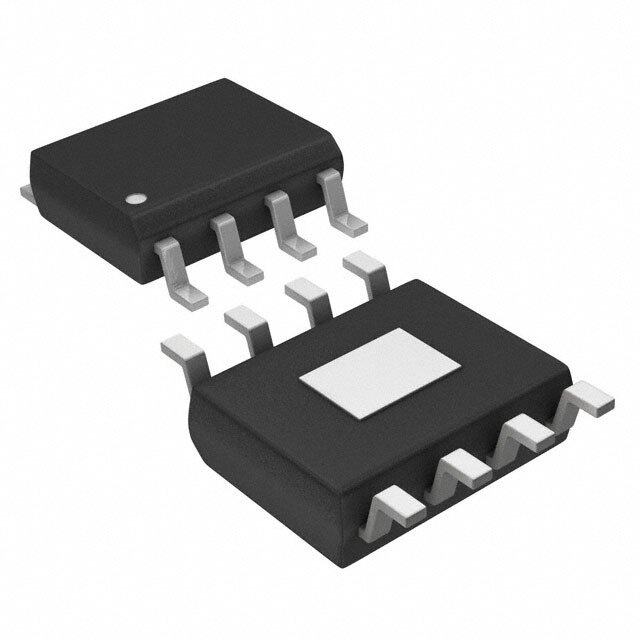
| 描述 | IC OPAMP PGA 12MHZ RRO 8SOIC特殊用途放大器 1-Chan. 12 MHz SPI |
| 产品分类 | Linear - Amplifiers - Instrumentation, OP Amps, Buffer Amps集成电路 - IC |
| 品牌 | Microchip Technology |
| 产品手册 | |
| 产品图片 |
|
| rohs | 符合RoHS无铅 / 符合限制有害物质指令(RoHS)规范要求 |
| 产品系列 | 放大器 IC,特殊用途放大器,Microchip Technology MCP6S21-I/SN- |
| 数据手册 | http://www.microchip.com/mymicrochip/filehandler.aspx?ddocname=en026002http://www.microchip.com/mymicrochip/filehandler.aspx?ddocname=en011661http://www.microchip.com/mymicrochip/filehandler.aspx?ddocname=en023833 |
| 产品型号 | MCP6S21-I/SN |
| PCN组件/产地 | http://www.microchip.com/mymicrochip/NotificationDetails.aspx?id=5774&print=view |
| PCN设计/规格 | http://www.microchip.com/mymicrochip/NotificationDetails.aspx?id=5576&print=viewhttp://www.microchip.com/mymicrochip/NotificationDetails.aspx?id=5704&print=viewhttp://www.microchip.com/mymicrochip/NotificationDetails.aspx?pcn=JAON-27WIZT300&print=view |
| 产品目录页面 | |
| 产品种类 | 特殊用途放大器 |
| 供应商器件封装 | 8-SOIC N |
| 其它名称 | MCP6S21ISN |
| 包装 | 管件 |
| 压摆率 | 22 V/µs |
| 商标 | Microchip Technology |
| 增益带宽积 | - |
| 安装类型 | 表面贴装 |
| 安装风格 | SMD/SMT |
| 封装 | Tube |
| 封装/外壳 | 8-SOIC(0.154",3.90mm 宽) |
| 封装/箱体 | SOIC-8 |
| 工作温度 | -40°C ~ 85°C |
| 工作电源电压 | 3 V, 5 V |
| 工厂包装数量 | 100 |
| 放大器类型 | 可编程增益 |
| 最大工作温度 | + 85 C |
| 最小工作温度 | - 40 C |
| 标准包装 | 100 |
| 电压-电源,单/双 (±) | 2.5 V ~ 5.5 V |
| 电压-输入失调 | 275µV |
| 电流-电源 | 1mA |
| 电流-输入偏置 | 1pA |
| 电流-输出/通道 | 30mA |
| 电源电压-最大 | 5.5 V |
| 电源电压-最小 | 2.5 V |
| 电路数 | 1 |
| 输入补偿电压 | 0.275 mV |
| 输出类型 | 满摆幅 |
| 通道数量 | 1 Channel |


- 商务部:美国ITC正式对集成电路等产品启动337调查
- 曝三星4nm工艺存在良率问题 高通将骁龙8 Gen1或转产台积电
- 太阳诱电将投资9.5亿元在常州建新厂生产MLCC 预计2023年完工
- 英特尔发布欧洲新工厂建设计划 深化IDM 2.0 战略
- 台积电先进制程称霸业界 有大客户加持明年业绩稳了
- 达到5530亿美元!SIA预计今年全球半导体销售额将创下新高
- 英特尔拟将自动驾驶子公司Mobileye上市 估值或超500亿美元
- 三星加码芯片和SET,合并消费电子和移动部门,撤换高东真等 CEO
- 三星电子宣布重大人事变动 还合并消费电子和移动部门
- 海关总署:前11个月进口集成电路产品价值2.52万亿元 增长14.8%


PDF Datasheet 数据手册内容提取
MCP6S21/2/6/8 Single-Ended, Rail-to-Rail I/O, Low Gain PGA Features Description • Multiplexed Inputs: 1, 2, 6 or 8 channels The Microchip Technology Inc. MCP6S21/2/6/8 are • 8 Gain Selections: analog Programmable Gain Amplifiers (PGA). They can be configured for gains from +1V/V to +32V/V and - +1, +2, +4, +5, +8, +10, +16 or +32V/V the input multiplexer can select one of up to eight chan- • Serial Peripheral Interface (SPI) nels through an SPI port. The serial interface can also • Rail-to-Rail Input and Output put the PGA into shutdown to conserve power. These • Low Gain Error: ±1% (max) PGAs are optimized for high speed, low offset voltage • Low Offset: ±275µV (max) and single-supply operation with rail-to-rail input and • High Bandwidth: 2 to 12MHz (typ) output capability. These specifications support single supply applications needing flexible performance or • Low Noise: 10nV/Hz @ 10kHz (typ) multiple inputs. • Low Supply Current: 1.0mA (typ) The one channel MCP6S21 and the two channel • Single Supply: 2.5V to 5.5V MCP6S22 are available in 8-pin PDIP, SOIC and Typical Applications MSOP packages. The six channel MCP6S26 is avail- able in 14-pin PDIP, SOIC and TSSOP packages. The • A/D Converter Driver eight channel MCP6S28 is available in 16-pin PDIP • Multiplexed Analog Applications and SOIC packages. All parts are fully specified from -40°C to +85°C. • Data Acquisition • Industrial Instrumentation Block Diagram • Test Equipment V • Medical Instrumentation DD CH0 Package Types + CH1 V CH2 OUT MCP6S21 MCP6S22 CH3 - R PDIP, SOIC, MSOP PDIP, SOIC, MSOP CH4 MUX e s VOUT 1 8 VDD VOUT 1 8 VDD CCHH56 RF isto CH0 2 7 SCK CH0 2 7 SCK CH7 Gain 8 r L a VREF 3 6 SI CH1 3 6 SI CS Switches dde VSS 4 5 CS VSS 4 5 CS SI SPI™ RG r (R SO Logic LA SCK D ) MCP6S26 MCP6S28 POR PDIP, SOIC, TSSOP PDIP, SOIC VOUT 1 14 VDD VOUT 1 16 VDD VSS VREF CH0 2 13 SCK CH0 2 15 SCK CH1 3 12 SO CH1 3 14SO CH2 4 11 SI CH2 4 13SI CH3 5 10 CS CH3 5 12CS CH4 6 9 VSS CH4 6 11 VSS CH5 7 8 VREF CH5 7 10VREF CH6 8 9 CH7 2003-2012 Microchip Technology Inc. DS21117B-page 1
MCP6S21/2/6/8 1.0 ELECTRICAL PIN FUNCTION TABLE CHARACTERISTICS Name Function Absolute Maximum Ratings † V Analog Output OUT CH0-CH7 Analog Inputs V - V .........................................................................7.0V DD SS All inputs and outputs.......................VSS - 0.3V to VDD +0.3V VSS Negative Power Supply Difference Input voltage........................................|VDD - VSS| VDD Positive Power Supply Output Short Circuit Current...................................continuous SCK SPI Clock Input Current at Input Pin2mA SI SPI Serial Data Input Current at Output and Supply Pins30mA SO SPI Serial Data Output Storage temperature.....................................-65°C to +150°C CS SPI Chip Select Junction temperature..................................................+150°C V External Reference Pin REF ESD protection on all pins (HBM;MM)2kV; 200V † Notice: Stresses above those listed under "Maximum Ratings" may cause permanent damage to the device. This is a stress rating only and functional operation of the device at those or any other conditions above those indicated in the operation listings of this specification is not implied. Exposure to maximum rating conditions for extended periods may affect device reliability. DC CHARACTERISTICS Electrical Specifications: Unless otherwise indicated, T =+25°C, V =+2.5V to +5.5V, V =GND, V = V , G=+1V/V, A DD SS REF SS Input=CH0=(0.3V)/G, CH1 to CH7=0.3V, R =10kto V /2, SI and SCK are tied low and CS is tied high. L DD Parameters Sym Min Typ Max Units Conditions Amplifier Input Input Offset Voltage V -275 — +275 µV G = +1, V = 4.0V OS DD Input Offset Voltage Drift V /T — ±4 — µV/°C T = -40 to +85°C OS A A Power Supply Rejection Ratio PSRR 70 85 — dB G = +1 (Note1) Input Bias Current I — ±1 — pA CHx = V /2 B DD Input Bias Current over I — — 250 pA T = -40 to +85°C, B A Temperature CHx = V /2 DD Input Impedance Z — 1013||15 — ||pF IN Input Voltage Range V V 0.3 — V +0.3 V IVR SS DD Amplifier Gain Nominal Gains — — 1 to 32 — V/V +1, +2, +4, +5, +8, +10, +16 or +32 DC Gain Error G = +1 g -0.1 — +0.1 % V 0.3V to V 0.3V E OUT DD G +2 g -1.0 — +1.0 % V 0.3V to V 0.3V E OUT DD DC Gain Drift G = +1 G/T — ±0.0002 — %/°C T = -40 to +85°C A A G +2 G/T — ±0.0004 — %/°C T = -40 to +85°C A A Internal Resistance R 3.4 4.9 6.4 k (Note1) LAD Internal Resistance over R /T — +0.028 — %/°C (Note1) LAD A Temperature T = -40 to +85°C A Amplifier Output DC Output Non-linearityG = +1 V — ±0.003 — % of FSR V = 0.3V to V 0.3V, V = 5.0V ONL OUT DD DD G +2 V — ±0.001 — % of FSR V = 0.3V to V 0.3V, V = 5.0V ONL OUT DD DD Maximum Output Voltage Swing V , V V +20 — V -100 mV G +2; 0.5V output overdrive OH OL SS DD V +60 — V -60 G +2; 0.5V output overdrive, SS DD V = V /2 REF DD Short-Circuit Current I — ±30 — mA O(SC) Note 1: R (R + R in Figure4-1) connects V , V and the inverting input of the internal amplifier. The MCP6S22 has LAD F G REF OUT V tied internally to V , so V is coupled to the internal amplifier and the PSRR spec describes PSRR+ only. We REF SS SS recommend the MCP6S22’s V pin be tied directly to ground to avoid noise problems. SS 2: I includes current in R (typically 60µA at V = 0.3V). Both I and I exclude digital switching currents. Q LAD OUT Q Q_SHDN 3: The output goes Hi-Z and the registers reset to their defaults; see Section5.4, “Power-On Reset”. DS21117B-page 2 2003-2012 Microchip Technology Inc.
MCP6S21/2/6/8 DC CHARACTERISTICS (CONTINUED) Electrical Specifications: Unless otherwise indicated, T =+25°C, V =+2.5V to +5.5V, V =GND, V = V , G=+1V/V, A DD SS REF SS Input=CH0=(0.3V)/G, CH1 to CH7=0.3V, R =10kto V /2, SI and SCK are tied low and CS is tied high. L DD Parameters Sym Min Typ Max Units Conditions Power Supply Supply Voltage V 2.5 — 5.5 V DD Quiescent Current I 0.5 1.0 1.35 mA I = 0 (Note2) Q O Quiescent Current, Shutdown I — 0.5 1.0 µA I = 0 (Note2) Q_SHDN O mode Power-On Reset POR Trip Voltage V 1.2 1.7 2.2 V (Note3) POR POR Trip Voltage Drift V /T — -3.0 — mV/°C T = -40°C to+85°C POR A Note 1: R (R + R in Figure4-1) connects V , V and the inverting input of the internal amplifier. The MCP6S22 has LAD F G REF OUT V tied internally to V , so V is coupled to the internal amplifier and the PSRR spec describes PSRR+ only. We REF SS SS recommend the MCP6S22’s V pin be tied directly to ground to avoid noise problems. SS 2: I includes current in R (typically 60µA at V = 0.3V). Both I and I exclude digital switching currents. Q LAD OUT Q Q_SHDN 3: The output goes Hi-Z and the registers reset to their defaults; see Section5.4, “Power-On Reset”. AC CHARACTERISTICS Electrical Specifications: Unless otherwise indicated, T =+25°C, V =+2.5V to +5.5V, V =GND, V = V , G=+1V/V, A DD SS REF SS Input = CH0 =(0.3V)/G, CH1 to CH7=0.3V, R =10kto V /2, C = 60 pF, SI and SCK are tied low, and CS is tied high. L DD L Parameters Sym Min Typ Max Units Conditions Frequency Response -3dB Bandwidth BW — 2 to 12 — MHz All gains; V < 100mV (Note1) OUT P-P Gain Peaking GPK — 0 — dB All gains; V < 100mV OUT P-P Total Harmonic Distortion plus Noise f = 1kHz, G = +1 V/V THD+N — 0.0015 — % V = 1.5V ± 1.0V , V = 5.0V, OUT PK DD BW = 22kHz f = 1kHz, G = +4 V/V THD+N — 0.0058 — % V = 1.5V ± 1.0V , V = 5.0V, OUT PK DD BW = 22kHz f = 1kHz, G = +16 V/V THD+N — 0.023 — % V = 1.5V ± 1.0V , V = 5.0V, OUT PK DD BW = 22kHz f = 20kHz, G = +1 V/V THD+N — 0.0035 — % V = 1.5V ± 1.0V , V = 5.0V, OUT PK DD BW = 80kHz f = 20kHz, G = +4 V/V THD+N — 0.0093 — % V = 1.5V ± 1.0V , V = 5.0V, OUT PK DD BW = 80kHz f = 20kHz, G = +16 V/V THD+N — 0.036 — % V = 1.5V ± 1.0V , V = 5.0V, OUT PK DD BW = 80kHz Step Response Slew Rate SR — 4.0 — V/µs G = 1, 2 — 11 — V/µs G = 4, 5, 8, 10 — 22 — V/µs G = 16, 32 Noise Input Noise Voltage E — 3.2 — µV f = 0.1Hz to 10kHz (Note2) ni P-P — 26 — f = 0.1Hz to 200kHz (Note2) Input Noise Voltage Density e — 10 — nV/Hz f = 10kHz (Note2) ni Input Noise Current Density i — 4 — fA/Hz f = 10kHz ni Note 1: See Table4-1 for a list of typical numbers. 2: E and e include ladder resistance noise. See Figure2-33 for e vs. G data. ni ni ni 2003-2012 Microchip Technology Inc. DS21117B-page 3
MCP6S21/2/6/8 DIGITAL CHARACTERISTICS Electrical Specifications: Unless otherwise indicated, T =+25°C, V =+2.5V to +5.5V, V =GND, V = V , G =+1V/V, A DD SS REF SS Input = CH0 = (0.3V)/G, CH1 to CH7 = 0.3V, R =10kto V /2, C = 60pF, SI and SCK are tied low, and CS is tied high. L DD L Parameters Sym Min Typ Max Units Conditions SPI Inputs (CS, SI, SCK) Logic Threshold, Low V 0 — 0.3V V IL DD Input Leakage Current I -1.0 — +1.0 µA IL Logic Threshold, High V 0.7V — V V IH DD DD Amplifier Output Leakage Current — -1.0 — +1.0 µA In Shutdown mode SPI Output (SO, for MCP6S26 and MCP6S28) Logic Threshold, Low V V — V +0.4 V I = 2.1mA, V = 5V OL SS SS OL DD Logic Threshold, High V V -0.5 — V V I = -400µA OH DD DD OH SPI Timing Pin Capacitance C — 10 — pF All digital I/O pins PIN Input Rise/Fall Times (CS, SI, SCK) tRFI — — 2 µs Note1 Output Rise/Fall Times (SO) t — 5 — ns MCP6S26 and MCP6S28 RFO CS high time tCSH 40 — — ns SCK edge to CS fall setup time tCS0 10 — — ns SCK edge when CS is high CS fall to first SCK edge setup time tCSSC 40 — — ns SCK Frequency f — — 10 MHz V = 5V (Note2) SCK DD SCK high time t 40 — — ns HI SCK low time t 40 — — ns LO SCK last edge to CS rise setup time tSCCS 30 — — ns CS rise to SCK edge setup time tCS1 100 — — ns SCK edge when CS is high SI set-up time t 40 — — ns SU SI hold time t 10 — — ns HD SCK to SO valid propagation delay t — — 80 ns MCP6S26 and MCP6S28 DO CS rise to SO forced to zero tSOZ — — 80 ns MCP6S26 and MCP6S28 Channel and Gain Select Timing Channel Select Time t — 1.5 — µs CHx = 0.6V, CHy =0.3V, G = 1, CH CHx to CHy select CS = 0.7V to V 90% point DD OUT Gain Select Time t — 1 — µs CHx = 0.3V, G = 5 to G = 1 select, G CS = 0.7V to V 90% point DD OUT Shutdown Mode Timing Out of Shutdown mode (CS goes tON — 3.5 10 µs CS = 0.7VDD to VOUT 90% point high) to Amplifier Output Turn-on Time Into Shutdown mode (CS goes high) tOFF — 1.5 — µs CS = 0.7VDD to VOUT 90% point to Amplifier Output High-Z Turn-off Time POR Timing Power-On Reset power-up time t — 30 — µs V = V - 0.1V to V + 0.1V, RPU DD POR POR 50% V to 90% V point DD OUT Power-On Reset power-down time t — 10 — µs V = V + 0.1V to V - 0.1V, RPD DD POR POR 50% V to 90% V point DD OUT Note 1: Not tested in production. Set by design and characterization. 2: When using the device in the daisy chain configuration, maximum clock frequency is determined by a combination of propagation delay time (t 80ns), data input setup time (t 40ns), SCK high time (t 40ns), and SCK rise and DO SU HI fall times of 5ns. Maximum f is, therefore, 5.8MHz. SCK DS21117B-page 4 2003-2012 Microchip Technology Inc.
MCP6S21/2/6/8 TEMPERATURE CHARACTERISTICS Electrical Specifications: Unless otherwise indicated, V =+2.5V to +5.5V, V =GND. DD SS Parameters Sym Min Typ Max Units Conditions Temperature Ranges Specified Temperature Range T -40 — +85 °C A Operating Temperature Range T -40 — +125 °C (Note1) A Storage Temperature Range T -65 — +150 °C A Thermal Package Resistances Thermal Resistance, 8L-PDIP — 85 — °C/W JA Thermal Resistance, 8L-SOIC — 163 — °C/W JA Thermal Resistance, 8L-MSOP — 206 — °C/W JA Thermal Resistance, 14L-PDIP — 70 — °C/W JA Thermal Resistance, 14L-SOIC — 120 — °C/W JA Thermal Resistance, 14L-TSSOP — 100 — °C/W JA Thermal Resistance, 16L-PDIP — 70 — °C/W JA Thermal Resistance, 16L-SOIC — 90 — °C/W JA Note 1: The MCP6S21/2/6/8 family of PGAs operates over this extended temperature range, but with reduced performance. Operation in this range must not cause T to exceed the Maximum Junction Temperature J (150°C). CS CS t t CH G 0.6V 1.5V V V OUT OUT 0.3V 0.3V FIGURE 1-1: Channel Select Timing FIGURE 1-3: Gain Select Timing Diagram. Diagram. CS VDD VPOR - 0.1V VPOR + 0.1V VPOR - 0.1V tON tOFF tRPU tRPD Hi-Z Hi-Z Hi-Z Hi-Z VOUT VOUT 0.3V 0.3V 1.0mA (typ) I ISS 1.0mA (typ) SS 500nA (typ) 500nA (typ) FIGURE 1-4: POR power-up and power- FIGURE 1-2: PGA Shutdown timing down timing diagram. diagram (must enter correct commands before CS goes high). 2003-2012 Microchip Technology Inc. DS21117B-page 5
MCP6S21/2/6/8 t CSH CS t t t t CSSC SCCS CS1 CS0 t t LO HI SCK 1/f tSU tHD SCK SI tDO tSOZ SO (first 16 bits out are always zeros) FIGURE 1-5: Detailed SPI Serial Interface Timing, SPI 0,0 mode. t CSH CS t t t t CSSC SCCS CS1 CS0 t t HI LO SCK 1/f t t SCK SU HD SI tDO tSOZ SO (first 16 bits out are always zeros) FIGURE 1-6: Detailed SPI Serial Interface Timing, SPI 1,1 mode. DS21117B-page 6 2003-2012 Microchip Technology Inc.
MCP6S21/2/6/8 1.1 DC Output Voltage Specs / Model V (V) OUT 1.1.1 IDEAL MODEL The ideal PGA output voltage (V ) is: OUT V DD EQUATION V -0.3 V2 DD V = GV V = V = 0V O_ideal IN REF SS T U where: G is the nominal gain V OV O_lineVarO_ideal (see Figure1-7). This equation holds when there are no gain or offset errors and when the VREF pin is tied to 0.3 V1 a low impedance source (<< 0.1) at ground potential (V = 0V). SS 0 V (V) IN 1.1.2 LINEAR MODEL 0 0.3 VDD - 0.3 VDD G G G The PGA’s linear region of operation, including offset and gain errors, is modeled by the line V , shown FIGURE 1-7: Output Voltage Model with O_linear in Figure1-7. the standard condition V = V = 0V. REF SS EQUATION 1.1.3 OUTPUT NON-LINEARITY V = G1+g V –0.3V+V +0.3V Figure1-8 shows the Integral Non-Linearity (INL) of the O_linear E IN OS output voltage. V = V = 0V REF SS EQUATION The endpoints of this line are at V =0.3V and O_ideal VDD-0.3V. The gain and offset specifications referred to INL = V –V OUT O_linear in the electrical specifications are related to Figure1-7, as follows: The output non-linearity specification in the electrical EQUATION specifications is related to Figure1-8 by: V –V g = 100%--------------2-------------1----------- EQUATION E GV –0.6V DD maxV V VOS = G--------1--V--+--1---g-------- G = +1 VONL = ---V----D----D----–----4-0---.-6----V3----- E g GT = --------E-- A TA INL (V) V 4 0 V 3 V (V) IN 0.3 V - 0.3 V 0 DD DD G G G FIGURE 1-8: Output Voltage INL with the standard condition V = V = 0V. REF SS 2003-2012 Microchip Technology Inc. DS21117B-page 7
MCP6S21/2/6/8 1.1.4 DIFFERENT V CONDITIONS REF Some of the plots in Section2.0, “Typical Performance Curves”, have the conditions V =V /2 or REF DD V =V . The equations and figures above are eas- REF DD ily modified for these conditions. The ideal V OUT becomes: EQUATION V = V +GV –V O_ideal REF IN REF V V V =0V DD REF SS The complete linear model is: EQUATION V = G1+g V –V +V +0.3V O_linear E IN IN_L OS where the new V endpoints are: IN EQUATION 0.3V–V V = ----------------------R---E---F-- IN_L G+V REF V –0.3V–V V = ----D----D-------------------------------R---E---F-- IN_R G+V REF The equations for extracting the specifications do not change. DS21117B-page 8 2003-2012 Microchip Technology Inc.
MCP6S21/2/6/8 2.0 TYPICAL PERFORMANCE CURVES Note: The graphs and tables provided following this note are a statistical summary based on a limited number of samples and are provided for informational purposes only. The performance characteristics listed herein are not tested or guaranteed. In some graphs or tables, the data presented may be outside the specified operating range (e.g., outside specified power supply range) and therefore outside the warranted range. Note: Unless otherwise indicated, T =+25°C, V =+5.0V, V =GND, V =V , G=+1V/V, A DD SS REF SS Input =CH0 =(0.3V)/G, CH1 to CH7 = 0.3V, R =10kto V /2, and C = 60pF. L DD L s 22% es 18% ge of Occurrence 1111120246808%%%%%%% 4G2 =0 +S1amples ge of Occurrenc 1111024668%%%%%% 4GT2A = 0= +S-14a0m tpol e+s125°C nta 6% nta 4% ce 4% ce 2% Per 02%% Per 0% 6 5 4 3 2 1 0 1 2 3 4 5 6 0.040 0.036 0.032 0.028 0.024 0.020 0.016 0.012 0.008 0.004 0.000 0.004 0.000 0.000 0.000 0.000 0.000 0.000 0.000 0.000 0.000 0.000 0.000 0.000 0.000 - - - - - - - - - - - - - - - - DC Gain Error (%) DC Gain Drift (%/°C) FIGURE 2-1: DC Gain Error, G = +1. FIGURE 2-4: DC Gain Drift, G = +1. 18% s 24% ntage of Occurrences 11114680246%%%%%%% 4G2 (cid:2)0 +S2amples centage of Occurrence 11111224680246802%%%%%%%%%% 4GT2A (cid:2) 0= +S -24a0m tpol e+s125°C Perce 02%% Per 02%% 20 16 12 08 04 00 04 08 12 16 20 0 0 0 0 0 0 0 0 0 0 0 5 4 3 2 1 0 1 2 3 4 5 0 0 0 0 0 0 0 0 0 0 0 0. 0. 0. 0. 0. 0. 0. 0. 0. 0. 0. 0. 0. 0. 0. 0. 0. 0. 0. 0. 0. 0. - - - - - - - - - - DC Gain Error (%) DC Gain Drift (%/°C) FIGURE 2-2: DC Gain Error, G +2. FIGURE 2-5: DC Gain Drift, G +2. 22% 20% currences 11124680%%%% 4T2A 0= S-4a0m tpol e+s125°C urrences 111468%%% 3VG6D =0D =+S 1a4m.0p Vles ge of Oc 11028%%% e of Occ 11028%%% centa 46%% entag 46%% Per 2% erc 2% 0% P 0% 3 4 5 6 7 8 9 0 1 2 2 2 2 2 2 2 3 3 0 0 0 0 0 0 0 0 0 0 0 0 0 0.0 0.0 0.0 0.0 0.0 0.0 0.0 0.0 0.0 -24 -20 -16 -12 -8 -4 4 8 12 16 20 24 Ladder Resistance Drift (%/°C) Input Offset Voltage (µV) FIGURE 2-3: Ladder Resistance Drift. FIGURE 2-6: Input Offset Voltage, V = 4.0V. DD 2003-2012 Microchip Technology Inc. DS21117B-page 9
MCP6S21/2/6/8 Note: Unless otherwise indicated, T =+25°C, V =+5.0V, V =GND, V =V , G=+1V/V, A DD SS REF SS Input =CH0 =(0.3V)/G, CH1 to CH7 = 0.3V, R =10kto V /2, and C = 60pF. L DD L 200 22% oltage (µV) 11505000 G = +1 Occurrences 1111224680%%%%% 4TG2A =0= +S-41a0m tpol e+s125°C et V 0 VDD = +2.5 e of 10% s -50 g 8% ut Off -100 VDD = +5.5 centa 46%% Inp -150 Per 2% -200 0% 6 4 2 0 8 6 4 2 0 2 4 6 8 0 2 4 6 0.0 0.5 1.0 1.5 2.0 2.5 3.0 3.5 4.0 4.5 5.0 5.5 -1 -1 -1 -1 - - - - 1 1 1 1 VREF Voltage (V) Input Offset Voltage Drift (µV/°C) FIGURE 2-7: Input Offset Voltage vs. FIGURE 2-10: Input Offset Voltage Drift. V Voltage. REF 0.01 0.0100% y, R) VOUT = 0.3V to VDD -0.3V y, VDD = +5.5 V utput Non-LinearitReferred (% of FS 00.0.000011 VVVOOONNNLLL///GGG,,, GGG (cid:2)== +++421 utput Non-Linearitput Referred (%) 0.0010% VONL/G, G = +1 C Oput C OIn VONL/G, G (cid:2) +2 Dn D I 0.00001 0.0001% 2.5 3.0 3.5 4.0 4.5 5.0 5.5 1 10 Power Supply Voltage (V) Output Voltage Swing (VP-P) FIGURE 2-8: DC Output Non-Linearity vs. FIGURE 2-11: DC Output Non-Linearity vs. Supply Voltage. Output Swing. 1000 12 y y 11 f = 10 kHz sit sit 10 n n e e 9 D D e 100 e 8 oise Voltag(cid:3)(nV/Hz) 10 oise Voltag(cid:3)(nV/Hz) 4567 N N 3 ut ut 2 p p n n 1 I I 1 0 00..11 11 1100 101000 1100k0 101000k0 101000000k 1 2 4 5 8 10 16 32 Frequency (Hz) Gain (V/V) FIGURE 2-9: Input Noise Voltage Density FIGURE 2-12: Input Noise Voltage Density vs. Frequency. vs. Gain. DS21117B-page 10 2003-2012 Microchip Technology Inc.
MCP6S21/2/6/8 Note: Unless otherwise indicated, T =+25°C, V =+5.0V, V =GND, V =V , G=+1V/V, A DD SS REF SS Input =CH0 =(0.3V)/G, CH1 to CH7 = 0.3V, R =10kto V /2, and C = 60pF. L DD L Power Supply Rejection Ratio (dB) 111789012000000 Power Supply Rejection Ratio (dB) 1056789000000 VVDDDD == 25..55 VV Input Referred 40 -50 -25 0 25 50 75 100 125 1100 101000 110k00 1010000k 101000000k Ambient Temperature (°C) Frequency (Hz) FIGURE 2-13: PSRR vs. Ambient FIGURE 2-16: PSRR vs. Frequency. Temperature. 1,000 10,000 CH0 = VDD VDD = 5.5 V A) VDD = 5.5 V A) Current (p 100 Current (p 1,100000 TA = +125°C Input Bias 10 Input Bias 10 TA = +85°C 1 1 55 65 75 85 95 105 115 125 0.0 0.5 1.0 1.5 2.0 2.5 3.0 3.5 4.0 4.5 5.0 5.5 Ambient Temperature (°C) Input Voltage (V) FIGURE 2-14: Input Bias Current vs. FIGURE 2-17: Input Bias Current vs. Input Ambient Temperature. Voltage. 100 7 6 G = +1 MHz) GG == ++14 g (dB)5 GG = = + +164 h ( G = +16 kin4 widt 10 Pea3 Band Gain 2 1 0 1 10 100 1000 10 100 1000 Capacitive Load (pF) Capacitive Load (pF) FIGURE 2-15: Bandwidth vs. Capacitive FIGURE 2-18: Gain Peaking vs. Capacitive Load. Load. 2003-2012 Microchip Technology Inc. DS21117B-page 11
MCP6S21/2/6/8 Note: Unless otherwise indicated, T =+25°C, V =+5.0V, V =GND, V =V , G=+1V/V, A DD SS REF SS Input =CH0 =(0.3V)/G, CH1 to CH7 = 0.3V, R =10kto V /2, and C = 60pF. L DD L 40 1.2 G = +32 1.1 30 G = +16 A) 1.0 m 20 nt ( 00..89 Gain (dB) 100 G = +10 G = +2 escent Curre 00000.....34567 TTTTAAAA ==== + ++ 1-28245550°°°°CCCC -10 GG == ++85 G = +1 Qui 0.2 G = +4 0.1 -20 0.0 11.E0+050k 11M.E+06 101.EM+07 1010.E+08M 0.0 0.5 1.0 1.5 2.0 2.5 3.0 3.5 4.0 4.5 5.0 5.5 Frequency (Hz) Supply Voltage (V) FIGURE 2-19: Gain vs. Frequency. FIGURE 2-22: Quiescent Current vs. Supply Voltage. es 10900%% 420 Samples wn 1.0 In Shutdown Mode urrenc 7800%% VDD = 5.0 V Shutdo 000...789 VDD = 5.0 V age of Occ 34560000%%%% Current in (µA) 000...456 cent 20% cent 00..23 Per 100%% uies 0.1 0 1 2 3 4 5 6 7 8 9 0 Q 0.0 0. 0. 0. 0. 0. 0. 0. 0. 0. 0. 1. -50 -25 0 25 50 75 100 125 Quiescent Current in Shutdown (µA) Ambient Temperature (°C) FIGURE 2-20: Histogram of Quiescent FIGURE 2-23: Quiescent Current in Current in Shutdown Mode. Shutdown Mode vs. Ambient Temperature. 100 40 V) nt m e 35 put Voltage Headroom (V- V and V - VDD OHOLSS 10 VDD =V +D5D. =5V +2.5V utput Short Circuit Curr(mA)11223050505 TTTTAAAA ==== + ++ 1-82245550°°°°CCCC ut O O 1 0 0.1 1 10 2.5 3.0 3.5 4.0 4.5 5.0 5.5 Output Current Magnitude (mA) Power Supply Voltage (V) FIGURE 2-21: Output Voltage Headroom FIGURE 2-24: Output Short Circuit Current vs. Output Current. vs. Supply Voltage. DS21117B-page 12 2003-2012 Microchip Technology Inc.
MCP6S21/2/6/8 Note: Unless otherwise indicated, T =+25°C, V =+5.0V, V =GND, V =V , G=+1V/V, A DD SS REF SS Input =CH0 =(0.3V)/G, CH1 to CH7 = 0.3V, R =10kto V /2, and C = 60pF. L DD L 1 1 Measurement BW = 80 kHz Measurement BW = 80 kHz VOUT = 2 VP-P VOUT = 4 VP-P VDD = 5.0 V VDD = 5.0 V %) %) e ( 0.1 e ( 0.1 s s Noi G = +16 Noi G = +16 + + HD 0.01 G = +4 HD 0.01 G = +4 T T G = +1 G = +1 0.001101.E+002 11.kE+03 101.E+k04 1001.E+0k5 0.001101.E+002 11.Ek+03 110.E+04k 1001.Ek+05 Frequency (Hz) Frequency (Hz) FIGURE 2-25: THD plus Noise vs. FIGURE 2-28: THD plus Noise vs. Frequency, V = 2V . Frequency, V = 4V . OUT P-P OUT P-P Output Voltage(10 mV/div)--211234567800000000000 V O U T , GGG === + ++3152 VDD =G +V5I.N0V ---05112211500505500000000Normalized Input Voltage (50 mV/div) Output Voltage (V) 0112233445..........5050505050 V O U T , GGG === + ++3152 VDD = +G5.V0IVN --0123456710........55555555..55Normalized Input Voltage(1V/div) -30 -200 0.00.00E+00 5.00E-07 1.00E-06 1.50E-06 2.00E-06 2.50E-06 3.00E-06 3.50E-06 4.00E-06 4.50E-06 5.00E--026.5 -04.000E+00 2.00E-07 4.00E-07 6.00E-07Tim8.00eE-07 (201.00E0-06 ns1.2/0E-d06iv)1.40E-06 1.60E-06 1.80E-06 2.00E--02650 Time (500 ns/div) FIGURE 2-26: Small Signal Pulse FIGURE 2-29: Large Signal Pulse Response. Response. 0.65 20 1.6 20 Output Voltage (V) 000000......344556505050 (CH0 = 0V.6OCVUT,S G = +1) (CH1 = 0V.3OCVUTS, G = +1) --05111505050 Chip Select Voltage (V) Output Voltage (V) 000111......468024 (CH0 = 0V.3OVUCT,S G = +5) (CH0 =C 0SV.3OVUT, G = +1) --05115015050 Chip Select Voltage (V) 0.30 -15 0.2 -15 0.250.00E+00 5.00E-07 1.00E-06 1.50E-06 2.00E-06 2.50E-06 3.00E-06 3.50E-06 4.00E-06 4.50E-06 5.00E--0260 0.00.00E+00 5.00E-07 1.00E-06 1.50E-06 2.00E-06 2.50E-06 3.00E-06 3.50E-06 4.00E-06 4.50E-06 5.00E--0260 Time (500 ns/div) Time (500 ns/div) FIGURE 2-27: Channel Select Timing. FIGURE 2-30: Gain Select Timing. 2003-2012 Microchip Technology Inc. DS21117B-page 13
MCP6S21/2/6/8 Note: Unless otherwise indicated, T =+25°C, V =+5.0V, V =GND, V =V , G=+1V/V, A DD SS REF SS Input =CH0 =(0.3V)/G, CH1 to CH7 = 0.3V, R =10kto V /2, and C = 60pF. L DD L 1.0 25 10 ut Voltage (mV) 000000......456789 ShCuStdown ShutdoCwSn -05112505050 Select Voltage (V) Voltage Swing (V)P-P 1 VVDDDD == 25..55 VV Outp 00..23 VOUT is "ON" --1150 Chip Output GG = =G + +4=1 t+6o1, ,++ +31220 0.1 (CH0 = 0.3V, G = +1) -20 0.1 0.00.0E+00 1.0E-06 2.0E-06 3.0E-06 4.0E-06 5.0E-06 6.0E-06 7.0E-06 8.0E-06 9.0E-06 1.0E-0-255 110.E+04k 101.E+005k 11.EM+06 101.ME+07 Time (1 µs/div) Frequency (Hz) FIGURE 2-31: Output Voltage vs. FIGURE 2-33: Output Voltage Swing vs. Shutdown Mode. Frequency. 20% 6 urrences 111468%%% 420 Samples ge (V) 45 VOUT VIN VGD =D +=1 5 V.0/V V ntage of Occ 110268%%%% Output Volta 23 erce 24%% put, 1 P 0% In 0 1.60 1.64 1.68 1.72 1.76 1.80 1.84 1.88 -1 0.0E+00 1.0E-03 2.0E-03 3.0E-03 4.0E-03 5.0E-03 6.0E-03 7.0E-03 8.0E-03 9.0E-03 1.0E-02 POR Trip Voltage (V) Time (1 ms/div) FIGURE 2-32: POR Trip Voltage. FIGURE 2-34: The MCP6S21/2/6/8 family shows no phase reversal under overdrive. DS21117B-page 14 2003-2012 Microchip Technology Inc.
MCP6S21/2/6/8 3.0 PIN DESCRIPTIONS The descriptions of the pins are listed in Table3-1. TABLE 3-1: PIN FUNCTION TABLE MCP6S21 MCP6S22 MCP6S26 MCP6S28 Symbol Description 1 1 1 1 V Analog Output OUT 2 2 2 2 CH0 Analog Input — 3 3 3 CH1 Analog Input — — 4 4 CH2 Analog Input — — 5 5 CH3 Analog Input — — 6 6 CH4 Analog Input — — 7 7 CH5 Analog Input — — — 8 CH6 Analog Input — — — 9 CH7 Analog Input 3 — 8 10 V External Reference Pin REF 4 4 9 11 V Negative Power Supply SS 5 5 10 12 CS SPI Chip Select 6 6 11 13 SI SPI Serial Data Input — — 12 14 SO SPI Serial Data Output 7 7 13 15 SCK SPI Clock Input 8 8 14 16 V Positive Power Supply DD 3.1 Analog Output 3.4 Power Supply (V and V ) SS DD The output pin (V ) is a low-impedance voltage The positive power supply pin (V ) is 2.5V to 5.5V OUT DD source. The selected gain (G), selected input (CH0- higher than the negative power supply pin (V ). For SS CH7) and voltage at V determine its value. normal operation, the other pins are between V and REF SS V . DD 3.2 Analog Inputs (CH0 thru CH7) Typically, these parts are used in a single (positive) The inputs CH0 through CH7 connect to the signal supply configuration. In this case, VSS is connected to sources. They are high-impedance CMOS inputs with ground and VDD is connected to the supply. VDD will low bias currents. The internal MUX selects which one need a local bypass capacitor (0.1µF) at the VDD pin. is amplified to the output. It can share a bulk capacitor with nearby analog parts (typically 2.2µF to 10µF within 4 inches (100mm) of 3.3 External Reference Voltage (V ) the V pin. REF DD The VREF pin should be at a voltage between VSS and 3.5 Digital Inputs V (the MCP6S22 has V tied internally to V ). DD REF SS The voltage at this pin shifts the output voltage. The SPI interface inputs are: Chip Select (CS), Serial Input (SI) and Serial Clock (SCK). These are Schmitt- triggered, CMOS logic inputs. 3.6 Digital Output The MCP6S26 and MCP6S28 devices have a SPI interface serial output (SO) pin. This is a CMOS push- pull output and does not ever go High-Z. Once the device is deselected (CS goes high), SO is forced low. This feature supports daisy chaining, as explained in Section5.3, “Daisy Chain Configuration”. 2003-2012 Microchip Technology Inc. DS21117B-page 15
MCP6S21/2/6/8 4.0 ANALOG FUNCTIONS 4.1 Input MUX The MCP6S21/2/6/8 family of Programmable Gain The MCP6S21 has one input, the MCP6S22 and Amplifiers (PGA) are based on simple analog building MCP6S25 have two inputs, the MCP6S26 has six blocks (see Figure4-1). Each of these blocks will be inputs and the MCP6S28 has eight inputs (see explained in more detail in the following sub-sections. Figure4-1). For the lowest input current, float unused inputs. Tying VDD these pins to a voltage near the used channels also works well. For simplicity, they can be tied to V or CH0 SS CH1 + V VDD, but the input current may increase. CH2 OUT - The one channel MCP6S21 has the lowest input bias CCHH34 MUX Re current, while the eight channel MCP6S28 has the s CCCHHH576 Gain 8 RF istor L hpaigrhtse.st. There is about a 2:1 ratio in IB between these a Switches d d 4.2 Internal Op Amp CS e SSOI SLPogI™ic RG Lr (R The internal op amp provides the right combination of A SCK D bandwidth, accuracy and flexibility. ) POR 4.2.1 COMPENSATION CAPACITORS VSS VREF The internal op amp has three compensation capaci- tors connected to a switching network. They are selected to give good small signal bandwidth at high MCP6S21–One input (CH0), no SO pin gains, and good slew rate (full power bandwidth) at low MCP6S22–Two inputs (CH0, CH1), V tied internally REF gains. The change in bandwidth as gain changes is to V , no SO pin SS between 2MHz and 12MHz. Refer to Table4-1 for MCP6S26–Six inputs (CH0 to CH5) more information. MCP6S28–Eight inputs (CH0 to CH7) FIGURE 4-1: PGA Block Diagram. TABLE 4-1: GAIN VS. INTERNAL COMPENSATION CAPACITOR Internal Gain Typical GBWP Typical SR Typical FPBW Typical BW Compensation (V/V) (MHz) (V/µs) (MHz) (MHz) Capacitor 1 Large 12 4.0 0.30 12 2 Large 12 4.0 0.30 6 4 Medium 20 11 0.70 10 5 Medium 20 11 0.70 7 8 Medium 20 11 0.70 2.4 10 Medium 20 11 0.70 2.0 16 Small 64 22 1.6 5 32 Small 64 22 1.6 2.0 Note 1: FPBW is the Full Power Bandwidth. These numbers are based on V = 5.0V. DD 2: No changes in DC performance (e.g., V ) accompany a change in compensation capacitor. OS 3: BW is the closed-loop, small signal -3dB bandwidth. DS21117B-page 16 2003-2012 Microchip Technology Inc.
MCP6S21/2/6/8 4.2.2 RAIL-TO-RAIL INPUT 4.3 Resistor Ladder The input stage of the internal op amp uses two differ- The resistor ladder shown in Figure4-1 (R = R + LAD F ential input stages in parallel; one operates at low VIN RG) sets the gain. Placing the gain switches in series (input voltage), while the other operates at high VIN. with the inverting input reduces the parasitic capaci- With this topology, the internal inputs can operate to tance, distortion and gain mismatch. 0.3V past either supply rail. The input offset voltage is R is an additional load on the output of the PGA and measured at both V =V - 0.3V and V + 0.3V to LAD IN SS DD causes additional current draw from the supplies. ensure proper operation. In Shutdown mode, R is still attached to the OUT The transition between the two input stages occurs LAD and V pins. Thus, these pins and the internal ampli- when V V - 1.5V. For the best distortion and gain REF IN DD fier’s inverting input are all connected through R linearity, avoid this region of operation. LAD and the output is not high-Z (unlike the external op amp). 4.2.3 RAIL-TO-RAIL OUTPUT While R contributes to the output noise, its effect is LAD The Maximum Output Voltage Swing is the maximum small. Refer to Figure2-12. swing possible under a particular output load. Accord- ing to the specification table, the output can reach 4.4 Shutdown Mode within 60mV of either supply rail when R =10kand L V = V /2. See Figure2-21 for typical performance These PGAs use a software shutdown command. REF DD under other conditions. When the SPI interface sends a shutdown command, the internal op amp is shut down and its output placed 4.2.4 INPUT VOLTAGE AND PHASE in a high-Z state. REVERSAL The resistive ladder is always connected between The amplifier family is designed with CMOS input VREF and VOUT; even in shutdown. This means that the devices. It is designed to not exhibit phase inversion output resistance will be on the order of 5k and there when the input pins exceed the supply voltages. will be a path for output signals to appear at the input. Figure2-34 shows an input voltage exceeding both The Power-on Reset (POR) circuitry will temporarily supplies with no resulting phase inversion. place the part in shutdown when activated. See The maximum voltage that can be applied to the input Section5.4, “Power-On Reset”, for details. pins (CHX) is V - 0.3V to V + 0.3V. Voltages on the SS DD inputs that exceed this absolute maximum rating can cause excessive current to flow in or out of the input pins. Current beyond ±2mA can cause possible reli- ability problems. Applications that exceed this rating must be externally limited with an input resistor, as shown in Figure4-2. RIN CHX VIN MCP6S2X VOUT Maximum expected V –V IN DD R ------------------------------------------------------------------------------- IN 2 mA V –Minimum expected V SS IN R ---------------------------------------------------------------------------- IN 2 mA FIGURE 4-2: R limits the current flow IN into an input pin. 2003-2012 Microchip Technology Inc. DS21117B-page 17
MCP6S21/2/6/8 5.0 DIGITAL FUNCTIONS CS is raised after one word (16 bits) to implement the desired changes. Section5.3, “Registers”, covers The MCP6S21/2/6/8 PGAs use a standard SPI com- applications using multiple 16-bit words. SO goes low patible serial interface to receive instructions from a after CS goes high; it has a push-pull output that does controller. This interface is configured to allow daisy not go into a high-Z state. chaining with other SPI devices. There is an internal POR (Power On Reset) that resets the registers under The MCP6S21/2/6/8 devices operate in SPI Modes 0,0 low power conditions. and 1,1. In 0,0 mode, the clock idles in the low state (Figure5-1) and, in 1,1 mode, the clock idles in the high 5.1 SPI Timing state (Figure5-2). In both modes, SI data is loaded into the PGA on the rising edge of SCK and SO data is Chip Select (CS) toggles low to initiate communication clocked out on the falling edge of SCK. In 0,0 mode, the with these devices. The first byte of each SI word (two falling edge of CS also acts as the first falling edge of bytes long) is the instruction byte, which goes into the SCK (see Figure5-1). There must be multiples of 16 Instruction Register. The Instruction Register points the clocks (SCK) while CS is low or commands will abort second byte to its destination. In a typical application, (see Section5.3, “Registers”). CS 1 2 3 4 5 6 7 8 9 10 11 12 13 14 15 16 SCK SI 7 0 7 0 bit bit bit bit Instruction Byte Data Byte SO (first 16 bits out are always zeros) FIGURE 5-1: Serial bus sequence for the PGA; SPI 0,0 mode (see Figure1-5). CS 1 2 3 4 5 6 7 8 9 10 11 12 13 14 15 16 SCK SI 7 0 7 0 bit bit bit bit Instruction Byte Data Byte SO (first 16 bits out are always zeros) FIGURE 5-2: Serial bus sequence for the PGA; SPI 1,1 mode (see Figure1-6). DS21117B-page 18 2003-2012 Microchip Technology Inc.
MCP6S21/2/6/8 5.2 Registers Thus, these devices are initially programmed with the Instruction Register set for NOP (no operation), a gain The analog functions are programmed through the SPI of +1V/V and CH0 as the input channel. interface using 16-bit words (see Figure5-1 and Figure5-2). This data is sent to two of three 8-bit regis- 5.2.1 INSTRUCTION REGISTER ters: Instruction Register (Register5-1), Gain Register (Register5-2) and Channel Register (Register5-3). The Instruction Register has 3 command bits and 1 indirect address bit; see Register5-1. The command The power-up defaults for these three registers are: bits include a NOP (000) to support daisy chaining (see • Instruction Register: 000xxxx0 Section5.3, “Registers”); the other NOP commands • Gain Register: xxxxx000 shown should not be used (they are reserved for future • Channel Register: xxxxx000 use). The device is brought out of Shutdown mode when a valid command, other than NOP or Shutdown, is sent and CS is raised. REGISTER 5-1: INSTRUCTION REGISTER W-0 W-0 W-0 U-x U-x U-x U-x W-0 M2 M1 M0 — — — — A0 bit 7 bit 0 bit 7-5 M2-M0: Command Bits 000 = NOP (Default) (Note1) 001 = PGA enters Shutdown Mode as soon as a full 16-bit word is sent and CS is raised. (Notes1 and2) 010 = Write to register. 011 = NOP (reserved for future use) (Note1) 1XX = NOP (reserved for future use) (Note1) bit 4-1 Unimplemented: Read as ‘0’ (reserved for future use) bit 0 A0: Indirect Address Bit 1 = Addresses the Channel Register 0 = Addresses the Gain Register (Default) Note 1: All other bits in the 16-bit word (including A0) are “don’t cares”. 2: The device exits Shutdown mode when a valid command (other than NOP or Shut- down) is sent and CS is raised; that valid command will be executed. Shutdown does not toggle. Legend: R = Readable bit W = Writable bit U = Unimplemented bit, read as ‘0’ -n = Value at POR ’1’ = Bit is set ’0’ = Bit is cleared x = Bit is unknown 2003-2012 Microchip Technology Inc. DS21117B-page 19
MCP6S21/2/6/8 5.2.2 SETTING THE GAIN The amplifier can be programmed to produce binary and decimal gain settings between +1V/V and +32V/V. Register5-2 shows the details. At the same time, differ- ent compensation capacitors are selected to optimize the bandwidth vs. slew rate trade-off (see Table4-1). REGISTER 5-2: GAIN REGISTER U-x U-x U-x U-x U-x W-0 W-0 W-0 — — — — — G2 G1 G0 bit 7 bit 0 bit 7-3 Unimplemented: Read as ‘0’ (reserved for future use) bit 2-0 G2-G0: Gain Select Bits 000 = Gain of +1 (Default) 001 = Gain of +2 010 = Gain of +4 011 = Gain of +5 100 = Gain of +8 101 = Gain of +10 110 = Gain of +16 111 = Gain of +32 Legend: R = Readable bit W = Writable bit U = Unimplemented bit, read as ‘0’ -n = Value at POR ’1’ = Bit is set ’0’ = Bit is cleared x = Bit is unknown DS21117B-page 20 2003-2012 Microchip Technology Inc.
MCP6S21/2/6/8 5.2.3 CHANGING THE CHANNEL If the instruction register is programmed to address the channel register, the multiplexed inputs of the MCP6S22, MCP6S26 and MCP6S28 can be changed per Register5-3. REGISTER 5-3: CHANNEL REGISTER U-x U-x U-x U-x U-x W-0 W-0 W-0 — — — — — C2 C1 C0 bit 7 bit 0 bit 7-3 Unimplemented: Read as ‘0’ (reserved for future use) bit 2-0 C2-C0: Channel Select Bits MCP6S21 MCP6S22 MCP6S26 MCP6S28 000 =CH0 (Default) CH0 (Default) CH0 (Default) CH0 (Default) 001 =CH0 CH1 CH1 CH1 001 =CH0 CH0 CH2 CH2 011 =CH0 CH1 CH3 CH3 100 =CH0 CH0 CH4 CH4 101 =CH0 CH1 CH5 CH5 110 =CH0 CH0 CH0 CH6 111 =CH0 CH1 CH0 CH7 Legend: R = Readable bit W = Writable bit U = Unimplemented bit, read as ‘0’ -n = Value at POR ’1’ = Bit is set ’0’ = Bit is cleared x = Bit is unknown 2003-2012 Microchip Technology Inc. DS21117B-page 21
MCP6S21/2/6/8 5.2.4 SHUTDOWN COMMAND The example in Figure5-3 shows a daisy chain config- uration with two devices, although any number of The software Shutdown command allows the user to devices can be configured this way. The MCP6S21 and put the amplifier into a low power mode (see MCP6S22 can only be used at the far end of the daisy Register5-1). In this shutdown mode, most pins are chain because they do not have a serial data out (SO) high impedance (Section4.4, “Shutdown Mode”, and pin. As shown in Figure5-4 and Figure5-5, both SI Section5.1, “SPI Timing”, cover the exceptions at pins and SO data are sent in 16-bit (2 byte) words. These V V and SO). REF, OUT devices abort any command that is not a multiple of 16 Once the PGA has entered shutdown mode, it will bits. remain in this mode until either a valid command is sent When using the daisy chain configuration, the maxi- to the device (other than NOP or Shutdown), or the mum clock speed possible is reduced to 5.8MHz device is powered down and back up again. The because of the SO pin’s propagation delay (see internal registers maintain their values while in Electrical Specifications). shutdown. The internal SPI shift register is automatically loaded Once brought out of shutdown mode, the part comes with zeros whenever CS goes high (a command is exe- back to its previous state (see Section5.4 for excep- cuted). Thus, the first 16-bits out of the SO pin once CS tions to this rule). This makes it possible to bring the line goes low are always zeros. This means that the device out of shutdown mode using one command; first command loaded into the next device in the daisy send a command to select the current channel (or gain) chain is a NOP. This feature makes it possible to send and the device will exit shutdown with the same state shorter command and data byte strings when the far- that existed before shutdown. thest devices do not need to change. For example, if there were three devices on the chain and only the mid- 5.3 Daisy Chain Configuration dle device needed changing, only 32 bytes of data Multiple devices can be connected in a daisy chain need to be transmitted (for the first and middle configuration by connecting the SO pin from one device devices), and the last device on the chain would to the SI pin on the next device and using common SCK receive a NOP when the CS pin is raised to execute the and CS lines (Figure5-3). This approach reduces PCB command. layout complexity. CS SCK PIC® SO CS CS Microcontroller SCK SCK SI SO SI SO Device 1 Device 2 1. Set CS low. 2. Clock out the instruction and data Device 1 Device 2 for Device 2 (16 clocks) to Device 1. 00100000 00000000 00000000 00000000 3. Device 1 automatically clocks out all zeros (first 16 clocks) to Device 2. 4. Clock out the instruction and data for Device 1 (16 clocks) to Device 1. 5. Device 1 automatically shifts data Device 1 Device 2 from Device 1 to Device 2 (16 01000001 00000111 00100000 00000000 clocks). 6. Raise CS. FIGURE 5-3: Daisy Chain Configuration. DS21117B-page 22 2003-2012 Microchip Technology Inc.
MCP6S21/2/6/8 CS 1 2 3 4 5 6 7 8 910111213141516 1 2 3 4 5 6 7 8 910111213141516 SCK SI 7 07 0 7 07 0 bit bit bit bit bit bit bit bit Instruction Byte Data Byte Instruction Byte Data Byte for Device 2 for Device 2 for Device 1 for Device 1 SO (first 16 bits out are always zeros) 7 07 0 bit bit bit bit Instruction Byte Data Byte for Device 2 for Device 2 FIGURE 5-4: Serial bus sequence for daisy-chain configuration; SPI 0,0 mode. CS 1 2 3 4 5 6 7 8 910111213141516 1 2 3 4 5 6 7 8 910111213141516 SCK SI 7 07 0 7 07 0 bit bit bit bit bit bit bit bit Instruction Byte Data Byte Instruction Byte Data Byte for Device 2 for Device 2 for Device 1 for Device 1 SO (first 16 bits out are always zeros) 7 07 0 bit bit bit bit Instruction Byte Data Byte for Device 2 for Device 2 FIGURE 5-5: Serial bus sequence for daisy-chain configuration; SPI 1,1 mode. 2003-2012 Microchip Technology Inc. DS21117B-page 23
MCP6S21/2/6/8 5.4 Power-On Reset If the power supply voltage goes below the POR trip voltage (V < V 1.7V), the internal POR circuit DD POR will reset all of the internal registers to their power-up defaults (this is a protection against low power supply voltages). The POR circuit also holds the part in shut- down mode while it is activated. It temporarily overrides the software shutdown status. The POR releases the shutdown circuitry once it is released (V > V ). DD POR A 0.1µF bypass capacitor mounted as close as possi- ble to the V pin provides additional transient DD immunity. DS21117B-page 24 2003-2012 Microchip Technology Inc.
MCP6S21/2/6/8 6.0 APPLICATIONS INFORMATION For C 100pF, a good estimate for R is 50. This L ISO value can be fine-tuned on the bench. Adjust R so ISO 6.1 Changing External Reference that the step response overshoot and frequency Voltage response peaking are acceptable at all gains. Figure6-1 shows a MCP6S21 with the V pin at 6.3 Layout Considerations REF 2.5V and V =5.0V. This allows the PGA to amplify DD Good PC board layout techniques will help achieve the signals centered on 2.5V, instead of ground-referenced performance shown in the Electrical Characteristics signals. The voltage reference MCP1525 is buffered by and Typical Performance Curves. It will also help a MCP6021, which gives a low output impedance ref- minimize EMC (Electro-Magnetic Compatibility) issues. erence voltage from DC to high frequencies. The source driving the V pin should have an output REF 6.3.1 COMPONENT PLACEMENT impedance of 0.1 to maintain reasonable gain accuracy. Separate circuit functions; digital from analog, low speed from high speed, and low power from high power, as this will reduce crosstalk. V DD Keep sensitive traces short and straight, separating V DD them from interfering components and traces. This is especially important for high frequency (low rise time) V V IN OUT signals. MCP6S21 MCP1525 V VREF Use a 0.1µF supply bypass capacitor within 0.1inch DD (2.5mm) of the V pin. It must connect directly to the DD 2.5V ground plane. A multi-layer ceramic chip capacitor, or REF high-frequency equivalent, works best. MCP6021 6.3.2 SIGNAL COUPLING 1µF The input pins of the MCP6S21/2/6/8 family of opera- tional amplifiers (op amps) are high-impedance. This makes them especially susceptible to capacitively-cou- FIGURE 6-1: PGA with Different External pled noise. Using a ground plane helps reduce this Reference Voltage. problem. When noise is capacitively-coupled, the ground plane 6.2 Capacitive Load and Stability provides additional shunt capacitance to ground. When Large capacitive loads can cause both stability prob- noise is magnetically coupled, the ground plane lems and reduced bandwidth for the MCP6S21/2/6/8 reduces the mutual inductance between traces. family of PGAs (Figure2-17 and Figure2-18). This Increasing the separation between traces makes a happens because a large load capacitance decreases significant difference. the internal amplifier’s phase margin and bandwidth. Changing the direction of one of the traces can also If the PGA drives a large capacitive load, the circuit in reduce magnetic coupling. It may help to locate guard Figure6-2 can be used. A small series resistor (R ) traces next to the victim trace. They should be on both ISO at the V improves the phase margin by making the sides of the victim trace and be as close as possible. OUT load resistive at high frequencies. It will not, however, Connect the guard traces to the ground plane at both improve the bandwidth. ends, and in the middle, of long traces. 6.3.3 HIGH FREQUENCY ISSUES Because the MCP6S21/2/6/8 PGAs reach unity gain R ISO near 64MHz when G = 16 and 32, it is important to use VIN MCP6S2X VOUT good PCB layout techniques. Any parasitic coupling at high frequency might cause undesired peaking. Filter- C ing high frequency signals (i.e., fast edge rates) can L help. To minimize high frequency problems: • Use complete ground and power planes • Use HF, surface mount components FIGURE 6-2: PGA Circuit for Large • Provide clean supply voltages and bypassing Capacitive Loads. • Keep traces short and straight • Try a linear power supply (e.g., an LDO) 2003-2012 Microchip Technology Inc. DS21117B-page 25
MCP6S21/2/6/8 6.4 Typical Applications V IN 6.4.1 GAIN RANGING Figure6-3 shows a circuit that measures the current I . MCP6021 X It benefits from changing the gain on the PGA. Just as 10.0k a hand-held multimeter uses different measurement ranges to obtain the best results, this circuit makes it V easy to set a high gain for small signals and a low gain OUT for large signals. As a result, the required dynamic MCP6S21 range at the PGA’s output is less than at its input (by up 1.11k to 30dB). FIGURE 6-5: PGA with lower gain range. MCP6S2X VOUT 6.4.3 EXTENDED GAIN RANGE PGA I Figure6-6 gives a +1V/V to +1024V/V gain range, X RS which is much greater than the range for a single PGA (+1V/V to +32V/V). The first PGA provides input mul- tiplexing capability, while the second PGA only needs one input. These devices can be daisy chained FIGURE 6-3: Wide Dynamic Range (Section5.3, “Daisy Chain Configuration”). Current Measurement Circuit. 6.4.2 SHIFTED GAIN RANGE PGA Figure6-4 shows a circuit using an MCP6021 at a gain of +10 in front of an MCP6S21. This changes the over- VIN MCP6S28 MCP6S21 VOUT all gain range to +10V/V to +320V/V (from +1V/V to +32V/V). FIGURE 6-6: PGA with Extended Gain Range. VIN MCP6021 MCP6S21 VOUT 6.4.4 MULTIPLE SENSOR AMPLIFIER The multiple channel PGAs (except the MCP6S21) allow the user to select which sensor appears on the output (see Figure6-7). These devices can also change the gain to optimize performance for each 10.0k sensor. 1.11k Sensor # 0 FIGURE 6-4: PGA with Modified Gain Sensor # 1 Range. MCP6S26 VOUT It is also easy to shift the gain range to lower gains (see Sensor # 5 Figure6-6). The MCP6021 acts as a unity gain buffer, and the resistive voltage divider shifts the gain range FIGURE 6-7: PGA with Multiple Sensor down to +0.1V/V to +3.2V/V (from +1V/V to +32V/V). Inputs. DS21117B-page 26 2003-2012 Microchip Technology Inc.
MCP6S21/2/6/8 6.4.5 EXPANDED INPUT PGA 6.4.7 ADC DRIVER Figure6-8 shows cascaded MCP6S28s that provide The family of PGA’s is well suited for driving Analog-to- up to 15 input channels. Obviously, Sensors #7-14 Digital Converters (ADC). The binary gains (1, 2, 4, 8, have a high total gain range available, as explained in 16 and 32) effectively add five more bits to the input Section6.4.3, “Extended Gain Range”. These devices range (see Figure6-10). This works well for applica- can be daisy chained (Section5.3, “Daisy Chain tions needing relative accuracy more than absolute Configuration”). accuracy (e.g., power monitoring). Lowpass Sensors Filter # 0-6 12 MCP6S28 VOUT VIN MCP6S28 MCP3201 OUT Sensors MCP6S28 # 7-14 FIGURE 6-10: PGA as an ADC Driver. FIGURE 6-8: PGA with Expanded Inputs. At low gains, the ADC’s Signal-to-Noise Ratio (SNR) will dominate since the PGAs input noise voltage den- 6.4.6 PIC MCU WITH EXPANDED INPUT sity is so low (10nV/Hz @ 10kHz, typ.). At high gains, CAPABILITY the PGA’s noise will dominate the SNR, but its low noise supports most applications. Again, these PGAs Figure6-9 shows an MCP6S28 driving an analog input add the flexibility of selecting the best gain for an to a PIC microcontroller. This greatly expands the input application. capacity of the microcontroller, while adding the ability The low pass filter in the block diagram reduces the to select the appropriate gain for each source. integrated noise at the MCP6S28’s output and serves as an anti-aliasing filter. This filter may be designed using Microchip’s FilterLab® software, available at www.microchip.com. PIC® VIN MCP6S28 Microcontroller SPI™ FIGURE 6-9: Expanded Input for a PIC® Microcontroller. 2003-2012 Microchip Technology Inc. DS21117B-page 27
MCP6S21/2/6/8 7.0 PACKAGING INFORMATION 7.1 Package Marking Information 8-Lead PDIP (300 mil) (MCP6S21, MCP6S22) Example: XXXXXXXX MCP6S21 XXXXXNNN I/P256 YYWW 0345 8-Lead SOIC (150 mil) (MCP6S21, MCP6S22) Example: XXXXXXXX MCP6S21 XXXXYYWW I/SN0345 NNN 256 8-Lead MSOP (MCP6S21, MCP6S22) Example: XXXXX MCP6S21I YWWNNN 345256 Legend: XX...X Customer specific information* YY Year code (last 2 digits of calendar year) WW Week code (week of January 1 is week ‘01’) NNN Alphanumeric traceability code Note: In the event the full Microchip part number cannot be marked on one line, it will be carried over to the next line thus limiting the number of available characters for customer specific information. * Standard marking consists of Microchip part number, year code, week code, traceability code (facility code, mask rev#, and assembly code). For marking beyond this, certain price adders apply. Please check with your Microchip Sales Office. DS21117B-page 28 2003-2012 Microchip Technology Inc.
MCP6S21/2/6/8 Package Marking Information (Con’t) 14-Lead PDIP (300 mil) (MCP6S26) Example: XXXXXXXXXXXXXX MCP6S26-I/P XXXXXXXXXXXXXX XXXXXXXXXXXXXX YYWWNNN 0345256 14-Lead SOIC (150 mil) (MCP6S26) Example: XXXXXXXXXXX MCP6S26ISL XXXXXXXXXXX XXXXXXXXXXXXXXXXXXXXXXXXX YYWWNNN 0345256 14-Lead TSSOP (4.4mm) (MCP6S26) Example: XXXXXXXX MCP6S26IST YYWW 0345 NNN 256 2003-2012 Microchip Technology Inc. DS21117B-page 29
MCP6S21/2/6/8 Package Marking Information (Con’t) 16-Lead PDIP (300 mil) (MCP6S28) Example: XXXXXXXXXXXXXX MCP6S28-I/P XXXXXXXXXXXXXX XXXXXXXXXXXXXX YYWWNNN 0345256 16-Lead SOIC (150 mil) (MCP6S28) Example: XXXXXXXXXXXXX MCP6S28-I/SL XXXXXXXXXXXXX XXXXXXXXXXXXXXXXXXXXXXXX YYWWNNN 0345256 DS21117B-page 30 2003-2012 Microchip Technology Inc.
MCP6S21/2/6/8 8-Lead Plastic Dual In-line (P) – 300 mil (PDIP) Note: For the most current package drawings, please see the Microchip Packaging Specification located at http://www.microchip.com/packaging E1 D 2 n 1 E A A2 L c A1 B1 p eB B Units INCHES* MILLIMETERS Dimension Limits MIN NOM MAX MIN NOM MAX Number of Pins n 8 8 Pitch p .100 2.54 Top to Seating Plane A .140 .155 .170 3.56 3.94 4.32 Molded Package Thickness A2 .115 .130 .145 2.92 3.30 3.68 Base to Seating Plane A1 .015 0.38 Shoulder to Shoulder Width E .300 .313 .325 7.62 7.94 8.26 Molded Package Width E1 .240 .250 .260 6.10 6.35 6.60 Overall Length D .360 .373 .385 9.14 9.46 9.78 Tip to Seating Plane L .125 .130 .135 3.18 3.30 3.43 Lead Thickness c .008 .012 .015 0.20 0.29 0.38 Upper Lead Width B1 .045 .058 .070 1.14 1.46 1.78 Lower Lead Width B .014 .018 .022 0.36 0.46 0.56 Overall Row Spacing § eB .310 .370 .430 7.87 9.40 10.92 Mold Draft Angle Top 5 10 15 5 10 15 Mold Draft Angle Bottom 5 10 15 5 10 15 * Controlling Parameter § Significant Characteristic Notes: Dimensions D and E1 do not include mold flash or protrusions. Mold flash or protrusions shall not exceed .010” (0.254mm) per side. JEDEC Equivalent: MS-001 Drawing No. C04-018 2003-2012 Microchip Technology Inc. DS21117B-page 31
MCP6S21/2/6/8 8-Lead Plastic Small Outline (SN) – Narrow, 150 mil (SOIC) Note: For the most current package drawings, please see the Microchip Packaging Specification located at http://www.microchip.com/packaging E E1 p D 2 B n 1 h 45 c A A2 L A1 Units INCHES* MILLIMETERS Dimension Limits MIN NOM MAX MIN NOM MAX Number of Pins n 8 8 Pitch p .050 1.27 Overall Height A .053 .061 .069 1.35 1.55 1.75 Molded Package Thickness A2 .052 .056 .061 1.32 1.42 1.55 Standoff § A1 .004 .007 .010 0.10 0.18 0.25 Overall Width E .228 .237 .244 5.79 6.02 6.20 Molded Package Width E1 .146 .154 .157 3.71 3.91 3.99 Overall Length D .189 .193 .197 4.80 4.90 5.00 Chamfer Distance h .010 .015 .020 0.25 0.38 0.51 Foot Length L .019 .025 .030 0.48 0.62 0.76 Foot Angle 0 4 8 0 4 8 Lead Thickness c .008 .009 .010 0.20 0.23 0.25 Lead Width B .013 .017 .020 0.33 0.42 0.51 Mold Draft Angle Top 0 12 15 0 12 15 Mold Draft Angle Bottom 0 12 15 0 12 15 * Controlling Parameter § Significant Characteristic Notes: Dimensions D and E1 do not include mold flash or protrusions. Mold flash or protrusions shall not exceed .010” (0.254mm) per side. JEDEC Equivalent: MS-012 Drawing No. C04-057 DS21117B-page 32 2003-2012 Microchip Technology Inc.
MCP6S21/2/6/8 8-Lead Plastic Micro Small Outline Package (MS) (MSOP) Note: For the most current package drawings, please see the Microchip Packaging Specification located at http://www.microchip.com/packaging E p E1 D 2 B n 1 A A2 c A1 (F) L Units INCHES MILLIMETERS* Dimension Limits MIN NOM MAX MIN NOM MAX Number of Pins n 8 8 Pitch p .026 0.65 Overall Height A .044 1.18 Molded Package Thickness A2 .030 .034 .038 0.76 0.86 0.97 Standoff § A1 .002 .006 0.05 0.15 Overall Width E .184 .193 .200 4.67 4.90 .5.08 Molded Package Width E1 .114 .118 .122 2.90 3.00 3.10 Overall Length D .114 .118 .122 2.90 3.00 3.10 Foot Length L .016 .022 .028 0.40 0.55 0.70 Footprint (Reference) F .035 .037 .039 0.90 0.95 1.00 Foot Angle 0 6 0 6 Lead Thickness c .004 .006 .008 0.10 0.15 0.20 Lead Width B .010 .012 .016 0.25 0.30 0.40 Mold Draft Angle Top 7 7 Mold Draft Angle Bottom 7 7 *Controlling Parameter § Significant Characteristic Notes: Dimensions D and E1 do not include mold flash or protrusions. Mold flash or protrusions shall not exceed .010" (0.254mm) per side. Drawing No. C04-111 2003-2012 Microchip Technology Inc. DS21117B-page 33
MCP6S21/2/6/8 14-Lead Plastic Dual In-line (P) – 300 mil (PDIP) Note: For the most current package drawings, please see the Microchip Packaging Specification located at http://www.microchip.com/packaging E1 D 2 n 1 E A A2 c L A1 B1 eB B p Units INCHES* MILLIMETERS Dimension Limits MIN NOM MAX MIN NOM MAX Number of Pins n 14 14 Pitch p .100 2.54 Top to Seating Plane A .140 .155 .170 3.56 3.94 4.32 Molded Package Thickness A2 .115 .130 .145 2.92 3.30 3.68 Base to Seating Plane A1 .015 0.38 Shoulder to Shoulder Width E .300 .313 .325 7.62 7.94 8.26 Molded Package Width E1 .240 .250 .260 6.10 6.35 6.60 Overall Length D .740 .750 .760 18.80 19.05 19.30 Tip to Seating Plane L .125 .130 .135 3.18 3.30 3.43 Lead Thickness c .008 .012 .015 0.20 0.29 0.38 Upper Lead Width B1 .045 .058 .070 1.14 1.46 1.78 Lower Lead Width B .014 .018 .022 0.36 0.46 0.56 Overall Row Spacing § eB .310 .370 .430 7.87 9.40 10.92 Mold Draft Angle Top 5 10 15 5 10 15 Mold Draft Angle Bottom 5 10 15 5 10 15 * Controlling Parameter § Significant Characteristic Notes: Dimensions D and E1 do not include mold flash or protrusions. Mold flash or protrusions shall not exceed .010” (0.254mm) per side. JEDEC Equivalent: MS-001 Drawing No. C04-005 DS21117B-page 34 2003-2012 Microchip Technology Inc.
MCP6S21/2/6/8 14-Lead Plastic Small Outline (SL) – Narrow, 150 mil (SOIC) Note: For the most current package drawings, please see the Microchip Packaging Specification located at http://www.microchip.com/packaging E E1 p D 2 B n 1 h 45 c A A2 A1 L Units INCHES* MILLIMETERS Dimension Limits MIN NOM MAX MIN NOM MAX Number of Pins n 14 14 Pitch p .050 1.27 Overall Height A .053 .061 .069 1.35 1.55 1.75 Molded Package Thickness A2 .052 .056 .061 1.32 1.42 1.55 Standoff § A1 .004 .007 .010 0.10 0.18 0.25 Overall Width E .228 .236 .244 5.79 5.99 6.20 Molded Package Width E1 .150 .154 .157 3.81 3.90 3.99 Overall Length D .337 .342 .347 8.56 8.69 8.81 Chamfer Distance h .010 .015 .020 0.25 0.38 0.51 Foot Length L .016 .033 .050 0.41 0.84 1.27 Foot Angle 0 4 8 0 4 8 Lead Thickness c .008 .009 .010 0.20 0.23 0.25 Lead Width B .014 .017 .020 0.36 0.42 0.51 Mold Draft Angle Top 0 12 15 0 12 15 Mold Draft Angle Bottom 0 12 15 0 12 15 * Controlling Parameter § Significant Characteristic Notes: Dimensions D and E1 do not include mold flash or protrusions. Mold flash or protrusions shall not exceed .010” (0.254mm) per side. JEDEC Equivalent: MS-012 Drawing No. C04-065 2003-2012 Microchip Technology Inc. DS21117B-page 35
MCP6S21/2/6/8 14-Lead Plastic Thin Shrink Small Outline (ST) – 4.4 mm (TSSOP) Note: For the most current package drawings, please see the Microchip Packaging Specification located at http://www.microchip.com/packaging E E1 p D 2 n 1 B A c A1 A2 L Units INCHES MILLIMETERS* Dimension Limits MIN NOM MAX MIN NOM MAX Number of Pins n 14 14 Pitch p .026 0.65 Overall Height A .043 1.10 Molded Package Thickness A2 .033 .035 .037 0.85 0.90 0.95 Standoff § A1 .002 .004 .006 0.05 0.10 0.15 Overall Width E .246 .251 .256 6.25 6.38 6.50 Molded Package Width E1 .169 .173 .177 4.30 4.40 4.50 Molded Package Length D .193 .197 .201 4.90 5.00 5.10 Foot Length L .020 .024 .028 0.50 0.60 0.70 Foot Angle 0 4 8 0 4 8 Lead Thickness c .004 .006 .008 0.09 0.15 0.20 Lead Width B1 .007 .010 .012 0.19 0.25 0.30 Mold Draft Angle Top 0 5 10 0 5 10 Mold Draft Angle Bottom 0 5 10 0 5 10 * Controlling Parameter § Significant Characteristic Notes: Dimensions D and E1 do not include mold flash or protrusions. Mold flash or protrusions shall not exceed .005” (0.127mm) per side. JEDEC Equivalent: MO-153 Drawing No. C04-087 DS21117B-page 36 2003-2012 Microchip Technology Inc.
MCP6S21/2/6/8 16-Lead Plastic Dual In-line (P) – 300 mil (PDIP) Note: For the most current package drawings, please see the Microchip Packaging Specification located at http://www.microchip.com/packaging E1 D 2 n 1 E A A2 c L A1 B1 eB B p Units INCHES* MILLIMETERS Dimension Limits MIN NOM MAX MIN NOM MAX Number of Pins n 16 16 Pitch p .100 2.54 Top to Seating Plane A .140 .155 .170 3.56 3.94 4.32 Molded Package Thickness A2 .115 .130 .145 2.92 3.30 3.68 Base to Seating Plane A1 .015 0.38 Shoulder to Shoulder Width E .300 .313 .325 7.62 7.94 8.26 Molded Package Width E1 .240 .250 .260 6.10 6.35 6.60 Overall Length D .740 .750 .760 18.80 19.05 19.30 Tip to Seating Plane L .125 .130 .135 3.18 3.30 3.43 Lead Thickness c .008 .012 .015 0.20 0.29 0.38 Upper Lead Width B1 .045 .058 .070 1.14 1.46 1.78 Lower Lead Width B .014 .018 .022 .036 0.46 0.56 Overall Row Spacing § eB .310 .370 .430 7.87 9.40 10.92 Mold Draft Angle Top 5 10 15 5 10 15 Mold Draft Angle Bottom 5 10 15 5 10 15 * Controlling Parameter § Significant Characteristic Notes: Dimensions D and E1 do not include mold flash or protrusions. Mold flash or protrusions shall not exceed .010” (0.254mm) per side. JEDEC Equivalent: MS-001 Drawing No. C04-017 2003-2012 Microchip Technology Inc. DS21117B-page 37
MCP6S21/2/6/8 16-Lead Plastic Small Outline (SL) – Narrow 150 mil (SOIC) Note: For the most current package drawings, please see the Microchip Packaging Specification located at http://www.microchip.com/packaging E E1 p D 2 B n 1 h 45 c A A2 L A1 Units INCHES* MILLIMETERS Dimension Limits MIN NOM MAX MIN NOM MAX Number of Pins n 16 16 Pitch p .050 1.27 Overall Height A .053 .061 .069 1.35 1.55 1.75 Molded Package Thickness A2 .052 .057 .061 1.32 1.44 1.55 Standoff § A1 .004 .007 .010 0.10 0.18 0.25 Overall Width E .228 .237 .244 5.79 6.02 6.20 Molded Package Width E1 .150 .154 .157 3.81 3.90 3.99 Overall Length D .386 .390 .394 9.80 9.91 10.01 Chamfer Distance h .010 .015 .020 0.25 0.38 0.51 Foot Length L .016 .033 .050 0.41 0.84 1.27 Foot Angle 0 4 8 0 4 8 Lead Thickness c .008 .009 .010 0.20 0.23 0.25 Lead Width B .013 .017 .020 0.33 0.42 0.51 Mold Draft Angle Top 0 12 15 0 12 15 Mold Draft Angle Bottom 0 12 15 0 12 15 * Controlling Parameter § Significant Characteristic Notes: Dimensions D and E1 do not include mold flash or protrusions. Mold flash or protrusions shall not exceed .010” (0.254mm) per side. JEDEC Equivalent: MS-012 Drawing No. C04-108 DS21117B-page 38 2003-2012 Microchip Technology Inc.
MCP6S21/2/6/8 PRODUCT IDENTIFICATION SYSTEM To order or obtain information, e.g., on pricing or delivery, refer to the factory or the listed sales office. PART NO. -X /XX Examples: Device Temperature Package a) MCP6S21-I/P: One Channel PGA, Range PDIP package. b) MCP6S21-I/SN: One Channel PGA, SOIC package. Device: MCP6S21: One Channel PGA c) MCP6S21-I/MS: One Channel PGA, MCP6S21T: One Channel PGA MSOP package. (Tape and Reel for SOIC and MSOP) MCP6S22: Two Channel PGA d) MCP6S22-I/MS: Two Channel PGA, MCP6S22T: Two Channel PGA MSOP package. (Tape and Reel for SOIC and MSOP) MCP6S26: Six Channel PGA e) MCP6S22T-I/MS: Tape and Reel, MCP6S26T: Six Channel PGA Two Channel PGA, MSOP package. (Tape and Reel for SOIC and TSSOP) f) MCP6S26-I/P: Six Channel PGA, MCP6S28: Eight Channel PGA PDIP package. MCP6S28T: Eight Channel PGA (Tape and Reel for SOIC) g) MCP6S26-I/SN: Six Channel PGA, SOIC package. h) MCP6S26T-I/ST: Tape and Reel, Temperature Range: I = -40°C to +85°C Six Channel PGA, TSSOP package. i) MCP6S28T-I/SL: Tape and Reel, Package: MS = Plastic Micro Small Outline (MSOP), 8-lead Eight Channel PGA, SOIC package. P = Plastic DIP (300 mil Body), 8, 14, and 16-lead SN = Plastic SOIC, (150 mil Body), 8-lead SL = Plastic SOIC (150 mil Body), 14, 16-lead ST = Plastic TSSOP (4.4mm Body), 14-lead Sales and Support Data Sheets Products supported by a preliminary Data Sheet may have an errata sheet describing minor operational differences and recom- mended workarounds. To determine if an errata sheet exists for a particular device, please contact one of the following: 1. Your local Microchip sales office 2. The Microchip Worldwide Site (www.microchip.com) Please specify which device, revision of silicon and Data Sheet (include Literature #) you are using. New Customer Notification System Register on our web site (www.microchip.com/cn) to receive the most current information on our products. 2003-2012 Microchip Technology Inc. DS21117B-page 39
MCP6S21/2/6/8 NOTES: DS21117B-page 40 2003-2012 Microchip Technology Inc.
Note the following details of the code protection feature on Microchip devices: • Microchip products meet the specification contained in their particular Microchip Data Sheet. • Microchip believes that its family of products is one of the most secure families of its kind on the market today, when used in the intended manner and under normal conditions. • There are dishonest and possibly illegal methods used to breach the code protection feature. All of these methods, to our knowledge, require using the Microchip products in a manner outside the operating specifications contained in Microchip’s Data Sheets. Most likely, the person doing so is engaged in theft of intellectual property. • Microchip is willing to work with the customer who is concerned about the integrity of their code. • Neither Microchip nor any other semiconductor manufacturer can guarantee the security of their code. Code protection does not mean that we are guaranteeing the product as “unbreakable.” Code protection is constantly evolving. We at Microchip are committed to continuously improving the code protection features of our products. Attempts to break Microchip’s code protection feature may be a violation of the Digital Millennium Copyright Act. If such acts allow unauthorized access to your software or other copyrighted work, you may have a right to sue for relief under that Act. Information contained in this publication regarding device Trademarks applications and the like is provided only for your convenience The Microchip name and logo, the Microchip logo, dsPIC, and may be superseded by updates. It is your responsibility to FlashFlex, KEELOQ, KEELOQ logo, MPLAB, PIC, PICmicro, ensure that your application meets with your specifications. PICSTART, PIC32 logo, rfPIC, SST, SST Logo, SuperFlash MICROCHIP MAKES NO REPRESENTATIONS OR and UNI/O are registered trademarks of Microchip Technology WARRANTIES OF ANY KIND WHETHER EXPRESS OR Incorporated in the U.S.A. and other countries. IMPLIED, WRITTEN OR ORAL, STATUTORY OR OTHERWISE, RELATED TO THE INFORMATION, FilterLab, Hampshire, HI-TECH C, Linear Active Thermistor, INCLUDING BUT NOT LIMITED TO ITS CONDITION, MTP, SEEVAL and The Embedded Control Solutions QUALITY, PERFORMANCE, MERCHANTABILITY OR Company are registered trademarks of Microchip Technology FITNESS FOR PURPOSE. Microchip disclaims all liability Incorporated in the U.S.A. arising from this information and its use. Use of Microchip Silicon Storage Technology is a registered trademark of devices in life support and/or safety applications is entirely at Microchip Technology Inc. in other countries. the buyer’s risk, and the buyer agrees to defend, indemnify and Analog-for-the-Digital Age, Application Maestro, BodyCom, hold harmless Microchip from any and all damages, claims, chipKIT, chipKIT logo, CodeGuard, dsPICDEM, suits, or expenses resulting from such use. No licenses are dsPICDEM.net, dsPICworks, dsSPEAK, ECAN, conveyed, implicitly or otherwise, under any Microchip ECONOMONITOR, FanSense, HI-TIDE, In-Circuit Serial intellectual property rights. Programming, ICSP, Mindi, MiWi, MPASM, MPF, MPLAB Certified logo, MPLIB, MPLINK, mTouch, Omniscient Code Generation, PICC, PICC-18, PICDEM, PICDEM.net, PICkit, PICtail, REAL ICE, rfLAB, Select Mode, SQI, Serial Quad I/O, Total Endurance, TSHARC, UniWinDriver, WiperLock, ZENA and Z-Scale are trademarks of Microchip Technology Incorporated in the U.S.A. and other countries. SQTP is a service mark of Microchip Technology Incorporated in the U.S.A. GestIC and ULPP are registered trademarks of Microchip Technology Germany II GmbH & Co. & KG, a subsidiary of Microchip Technology Inc., in other countries. All other trademarks mentioned herein are property of their respective companies. © 2003-2012, Microchip Technology Incorporated, Printed in the U.S.A., All Rights Reserved. Printed on recycled paper. ISBN: 9781620767504 QUALITY MANAGEMENT SYSTEM Microchip received ISO/TS-16949:2009 certification for its worldwide headquarters, design and wafer fabrication facilities in Chandler and CERTIFIED BY DNV Tempe, Arizona; Gresham, Oregon and design centers in California and India. The Company’s quality system processes and procedures == ISO/TS 16949 == are for its PIC® MCUs and dsPIC® DSCs, KEELOQ® code hopping devices, Serial EEPROMs, microperipherals, nonvolatile memory and analog products. In addition, Microchip’s quality system for the design and manufacture of development systems is ISO 9001:2000 certified. 2003-2012 Microchip Technology Inc. DS21117B-page 41
Worldwide Sales and Service AMERICAS ASIA/PACIFIC ASIA/PACIFIC EUROPE Corporate Office Asia Pacific Office India - Bangalore Austria - Wels 2355 West Chandler Blvd. Suites 3707-14, 37th Floor Tel: 91-80-3090-4444 Tel: 43-7242-2244-39 Chandler, AZ 85224-6199 Tower 6, The Gateway Fax: 91-80-3090-4123 Fax: 43-7242-2244-393 Tel: 480-792-7200 Harbour City, Kowloon India - New Delhi Denmark - Copenhagen Fax: 480-792-7277 Hong Kong Tel: 91-11-4160-8631 Tel: 45-4450-2828 Technical Support: Tel: 852-2401-1200 Fax: 91-11-4160-8632 Fax: 45-4485-2829 http://www.microchip.com/ support Fax: 852-2401-3431 India - Pune France - Paris Web Address: Australia - Sydney Tel: 91-20-2566-1512 Tel: 33-1-69-53-63-20 www.microchip.com Tel: 61-2-9868-6733 Fax: 91-20-2566-1513 Fax: 33-1-69-30-90-79 Atlanta Fax: 61-2-9868-6755 Japan - Osaka Germany - Munich Duluth, GA China - Beijing Tel: 81-66-152-7160 Tel: 49-89-627-144-0 Tel: 86-10-8569-7000 Fax: 49-89-627-144-44 Tel: 678-957-9614 Fax: 81-66-152-9310 Fax: 678-957-1455 Fax: 86-10-8528-2104 Japan - Yokohama Italy - Milan China - Chengdu Tel: 39-0331-742611 Boston Tel: 81-45-471- 6166 Tel: 86-28-8665-5511 Fax: 39-0331-466781 Westborough, MA Fax: 81-45-471-6122 Tel: 774-760-0087 Fax: 86-28-8665-7889 Korea - Daegu Netherlands - Drunen Fax: 774-760-0088 China - Chongqing Tel: 82-53-744-4301 Tel: 31-416-690399 Chicago Tel: 86-23-8980-9588 Fax: 82-53-744-4302 Fax: 31-416-690340 Itasca, IL Fax: 86-23-8980-9500 Korea - Seoul Spain - Madrid Tel: 630-285-0071 China - Hangzhou Tel: 82-2-554-7200 Tel: 34-91-708-08-90 Fax: 630-285-0075 Tel: 86-571-2819-3187 Fax: 82-2-558-5932 or Fax: 34-91-708-08-91 Cleveland Fax: 86-571-2819-3189 82-2-558-5934 UK - Wokingham Independence, OH China - Hong Kong SAR Malaysia - Kuala Lumpur Tel: 44-118-921-5869 Tel: 216-447-0464 Tel: 852-2401-1200 Tel: 60-3-6201-9857 Fax: 44-118-921-5820 Fax: 216-447-0643 Fax: 852-2401-3431 Fax: 60-3-6201-9859 Dallas China - Nanjing Malaysia - Penang Addison, TX Tel: 86-25-8473-2460 Tel: 60-4-227-8870 Tel: 972-818-7423 Fax: 86-25-8473-2470 Fax: 60-4-227-4068 Fax: 972-818-2924 China - Qingdao Philippines - Manila Detroit Tel: 86-532-8502-7355 Tel: 63-2-634-9065 Farmington Hills, MI Fax: 86-532-8502-7205 Fax: 63-2-634-9069 Tel: 248-538-2250 Fax: 248-538-2260 China - Shanghai Singapore Tel: 86-21-5407-5533 Tel: 65-6334-8870 Indianapolis Fax: 86-21-5407-5066 Fax: 65-6334-8850 Noblesville, IN Tel: 317-773-8323 China - Shenyang Taiwan - Hsin Chu Fax: 317-773-5453 Tel: 86-24-2334-2829 Tel: 886-3-5778-366 Fax: 86-24-2334-2393 Fax: 886-3-5770-955 Los Angeles Mission Viejo, CA China - Shenzhen Taiwan - Kaohsiung Tel: 949-462-9523 Tel: 86-755-8203-2660 Tel: 886-7-213-7828 Fax: 949-462-9608 Fax: 86-755-8203-1760 Fax: 886-7-330-9305 Santa Clara China - Wuhan Taiwan - Taipei Santa Clara, CA Tel: 86-27-5980-5300 Tel: 886-2-2508-8600 Tel: 408-961-6444 Fax: 86-27-5980-5118 Fax: 886-2-2508-0102 Fax: 408-961-6445 China - Xian Thailand - Bangkok Toronto Tel: 86-29-8833-7252 Tel: 66-2-694-1351 Mississauga, Ontario, Fax: 86-29-8833-7256 Fax: 66-2-694-1350 Canada China - Xiamen Tel: 905-673-0699 Tel: 86-592-2388138 Fax: 905-673-6509 Fax: 86-592-2388130 China - Zhuhai Tel: 86-756-3210040 10/26/12 Fax: 86-756-3210049 DS21117B-page 42 2003-2012 Microchip Technology Inc.