ICGOO在线商城 > 集成电路(IC) > 线性 - 放大器 - 仪表,运算放大器,缓冲器放大器 > OPA4345UA

 Datasheet下载
- 型号: OPA4345UA
- 制造商: Texas Instruments
- 库位|库存: xxxx|xxxx
- 要求:
| 数量阶梯 | 香港交货 | 国内含税 |
| +xxxx | $xxxx | ¥xxxx |
查看当月历史价格
查看今年历史价格
OPA4345UA产品简介:
ICGOO电子元器件商城为您提供OPA4345UA由Texas Instruments设计生产,在icgoo商城现货销售,并且可以通过原厂、代理商等渠道进行代购。 OPA4345UA价格参考¥10.23-¥20.87。Texas InstrumentsOPA4345UA封装/规格:线性 - 放大器 - 仪表,运算放大器,缓冲器放大器, General Purpose Amplifier 4 Circuit Rail-to-Rail 14-SOIC。您可以下载OPA4345UA参考资料、Datasheet数据手册功能说明书,资料中有OPA4345UA 详细功能的应用电路图电压和使用方法及教程。
OPA4345UA是Texas Instruments(德州仪器)推出的一款低噪声、轨至轨输入/输出、精密CMOS运算放大器,属于线性放大器中的运算放大器类别。该器件具有宽电源电压范围(2.7V至5.5V)、低静态电流和高带宽(1.8MHz),适用于对精度和功耗有较高要求的便携式与工业应用。

典型应用场景包括:
1. 便携式医疗设备:如心电图(ECG)、血糖仪等,得益于其低噪声和高精度特性,可准确放大微弱生物电信号。
2. 传感器信号调理:广泛用于压力、温度、光强等传感器的信号放大与处理,支持轨至轨输入输出,能充分利用供电范围,提升动态性能。
3. 数据采集系统:在多通道ADC前置放大电路中,OPA4345UA可提供高输入阻抗和低失真,确保信号完整性。
4. 电池供电设备:因其低功耗特性,适用于手持仪表、无线传感器节点等需延长电池寿命的设备。
5. 工业控制与过程控制:用于模拟信号处理模块,如4-20mA电流环接收端信号转换与放大。

此外,OPA4345UA采用14引脚TSSOP封装,集成四个独立放大器,适合空间受限但需多通道设计的应用。其优异的直流精度(低失调电压、低温漂)和交流性能,使其在中高端精密模拟电路中表现可靠。
| 参数 | 数值 |
| -3db带宽 | - |
| 产品目录 | 集成电路 (IC)半导体 |
| 描述 | IC OPAMP GP 3MHZ RRO 14SOIC运算放大器 - 运放 Lo Pwr Single-Sply Rail-to-Rail |
| 产品分类 | Linear - Amplifiers - Instrumentation, OP Amps, Buffer Amps集成电路 - IC |
| 品牌 | Texas Instruments |
| 产品手册 | http://www.ti.com/litv/sbos107a |
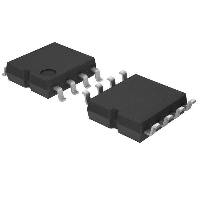
| 产品图片 |
|
| rohs | 符合RoHS无铅 / 符合限制有害物质指令(RoHS)规范要求 |
| 产品系列 | 放大器 IC,运算放大器 - 运放,Texas Instruments OPA4345UAMicroAmplifier™ |
| 数据手册 | |
| 产品型号 | OPA4345UA |
| 产品目录页面 | |
| 产品种类 | 运算放大器 - 运放 |
| 供应商器件封装 | 14-SOIC |
| 共模抑制比—最小值 | 66 dB |
| 关闭 | No Shutdown |
| 包装 | 管件 |
| 单位重量 | 129.400 mg |
| 压摆率 | 2 V/µs |
| 商标 | Texas Instruments |
| 增益带宽生成 | 3 MHz |
| 增益带宽积 | 3MHz |
| 安装类型 | 表面贴装 |
| 安装风格 | SMD/SMT |
| 封装 | Tube |
| 封装/外壳 | 14-SOIC(0.154",3.90mm 宽) |
| 封装/箱体 | SOIC-14 |
| 工作温度 | -40°C ~ 85°C |
| 工作电源电压 | 2.7 V to 5.5 V |
| 工厂包装数量 | 50 |
| 技术 | CMOS |
| 放大器类型 | 通用 |
| 最大工作温度 | + 85 C |
| 最小工作温度 | - 40 C |
| 标准包装 | 50 |
| 电压-电源,单/双 (±) | 2.5 V ~ 5.5 V |
| 电压-输入失调 | 200µV |
| 电流-电源 | 150µA |
| 电流-输入偏置 | 0.2pA |
| 电流-输出/通道 | 15mA |
| 电源电流 | 1 mA |
| 电路数 | 4 |
| 系列 | OPA4345 |
| 设计资源 | http://www.digikey.com/product-highlights/cn/zh/texas-instruments-webench-design-center/3176 |
| 转换速度 | 2 V/us |
| 输入偏压电流—最大 | 10 pA |
| 输入参考电压噪声 | 30 nV |
| 输入补偿电压 | 1 mV |
| 输出类型 | 满摆幅 |
| 通道数量 | 4 Channel |


- 商务部:美国ITC正式对集成电路等产品启动337调查
- 曝三星4nm工艺存在良率问题 高通将骁龙8 Gen1或转产台积电
- 太阳诱电将投资9.5亿元在常州建新厂生产MLCC 预计2023年完工
- 英特尔发布欧洲新工厂建设计划 深化IDM 2.0 战略
- 台积电先进制程称霸业界 有大客户加持明年业绩稳了
- 达到5530亿美元!SIA预计今年全球半导体销售额将创下新高
- 英特尔拟将自动驾驶子公司Mobileye上市 估值或超500亿美元
- 三星加码芯片和SET,合并消费电子和移动部门,撤换高东真等 CEO
- 三星电子宣布重大人事变动 还合并消费电子和移动部门
- 海关总署:前11个月进口集成电路产品价值2.52万亿元 增长14.8%


PDF Datasheet 数据手册内容提取
OPA344 OPA2344 OPA4344 OPA4344 OPA344 OPA345 OPA345 OPA2345 OPA342® OPA4345 www.ti.com SBOS107A – APRIL 2000 – REVISED AUGUST 2008 LOW POWER, SINGLE-SUPPLY, RAIL-TO-RAIL OPERATIONAL AMPLIFIERS Amplifier Series Micro ™ FEATURES DESCRIPTION (cid:1) RAIL-TO-RAIL INPUT The OPA344 and OPA345 series rail-to-rail CMOS (cid:1) RAIL-TO-RAIL OUTPUT (within 1mV) operational amplifiers are designed for precision, low-power, (cid:1) LOW QUIESCENT CURRENT: 150µA typ miniature applications. The OPA344 is unity gain stable, while the OPA345 is optimized for gains greater than or equal (cid:1) MicroSIZE PACKAGES to five, and has a gain-bandwidth product of 3MHz. SOT23-5 The OPA344 and OPA345 are optimized to operate on a MSOP-8 single supply from 2.5V and up to 5.5V with an input TSSOP-14 common-mode voltage range that extends 300mV (cid:1) GAIN-BANDWIDTH beyond the supplies. Quiescent current is only ≥ 250µA (max). OPA344: 1MHz, G 1 ≥ Rail-to-rail input and output make them ideal for driving OPA345: 3MHz, G 5 sampling analog-to-digital converters. They are also well suited (cid:1) SLEW RATE for general purpose and audio applications and providing I/V µ OPA344: 0.8V/ s conversion at the output of D/A converters. Single, dual and OPA345: 2V/µs quad versions have identical specs for design flexibility. (cid:1) THD + NOISE: 0.006% A variety of packages are available. All are specified for operation from –40ºC to 85ºC. A SPICE macromodel for APPLICATIONS design analysis is available for download from www.ti.com. (cid:1) PCMCIA CARDS OPA344, OPA345 (cid:1) DATA ACQUISITION (cid:1) PROCESS CONTROL Out 1 5 V+ (cid:1) AUDIO PROCESSING V– 2 (cid:1) COMMUNICATIONS OPA4344, OPA4345 +In 3 4 –In (cid:1) ACTIVE FILTERS (cid:1) TEST EQUIPMENT Out A 1 14 Out D SOT23-5 –In A 2 13 –In D OPA2344, OPA2345 OPA344, OPA345 A D +In A 3 12 +In D Out A 1 8 V+ NC 1 8 NC +V 4 11 –V A –In A 2 7 Out B –In 2 7 V+ +In B 5 10 +In C B C B +In A 3 6 –In B +In 3 6 Out –In B 6 9 –In C V– 4 5 +In B V– 4 5 NC Out B 7 8 Out C SO-8, MSOP-8, 8-Pin DIP (OPA2344 Only) SO-8, 8-Pin DIP (OPA344 Only) TSSOP-14, SO-14, 14-PIn DIP (OPA4344 Only) Please be aware that an important notice concerning availability, standard warranty, and use in critical applications of Texas Instruments semiconductor products and disclaimers thereto appears at the end of this data sheet. All trademarks are the property of their respective owners. PRODUCTION DATA information is current as of publication date. Copyright © 2000-2008, Texas Instruments Incorporated Products conform to specifications per the terms of Texas Instruments standard warranty. Production processing does not necessarily include testing of all parameters. www.ti.com
SPECIFICATIONS: V = 2.7V to 5.5V S At T = +25°C, R = 10kΩ connected to V /2 and V = V /2, unless otherwise noted. A L S OUT S Boldface limits apply over the temperature range, T = –40°C to +85°C. A OPA344NA, UA, PA OPA2344EA, UA, PA OPA4344EA, UA, PA PARAMETER CONDITION MIN TYP MAX UNITS OFFSET VOLTAGE Input Offset Voltage V V = +5.5V, V = V /2 ±0.2 ±1 mV OS S CM S Over Temperature ±0.8 ±1.2 mV vs Temperature dV /dT ±3 µV/°C OS vs Power Supply PSRR V = 2.7V to 5.5V, V < (V+) -1.8V 30 200 µV/V S CM Over Temperature V = 2.7V to 5.5V, V < (V+) -1.8V 250 µV/V S CM Channel Separation, dc 0.2 µV/V f = 1kHz 130 dB INPUT BIAS CURRENT Input Bias Current I ±0.2 ±10 pA B Over Temperature See Typical Curve pA Input Offset Current I ±0.2 ±10 pA OS NOISE Input Voltage Noise f = 0.1 to 50kHz 8 µVrms Input Voltage Noise Density e f = 10kHz 30 nV/√Hz n Current Noise Density i f = 10kHz 0.5 fA/√Hz n INPUT VOLTAGE RANGE Common-Mode Voltage Range V –0.3 (V+) + 0.3 V CM Common-Mode Rejection Ratio CMRR V = +5.5V, –0.3V< V < (V+)-1.8 76 92 dB S CM Over Temperature V = +5.5V, –0.3V< V < (V+)-1.8 74 dB S CM Common-Mode Rejection CMRR V = +5.5V, –0.3V< V < 5.8V 70 84 dB S CM Over Temperature V = +5.5V, –0.3V< V < 5.8V 68 dB S CM Common-Mode Rejection CMRR V = +2.7V, –0.3V< V < 3V 66 80 dB S CM Over Temperature V = +2.7V, –0.3V< V < 3V 64 dB S CM INPUT IMPEDANCE Differential 1013 || 3 Ω || pF Common-Mode 1013 || 6 Ω || pF OPEN-LOOP GAIN Open-Loop Voltage Gain A R = 100kΩ, 10mV < V < (V+) –10mV 104 122 dB OL L O Over Temperature R = 100kΩ, 10mV < V < (V+) –10mV 100 dB L O R = 5kΩ, 400mV < V < (V+) –400mV 96 120 dB L O Over Temperature R = 5kΩ, 400mV < V < (V+) –400mV 90 dB L O FREQUENCY RESPONSE C = 100pF L Gain-Bandwidth Product GBW 1 MHz Slew Rate SR 0.8 V/µs Settling Time, 0.1% V = 5.5V, 2V Step 5 µs S 0.01% V = 5.5V, 2V Step 8 µs S Overload Recovery Time V • G = V 2.5 µs IN S Total Harmonic Distortion + Noise THD+N V = 5.5V, V = 3Vp-p, G = 1, f = 1kHz 0.006 % S O OUTPUT Voltage Output Swing from Rail(1) R = 100kΩ, A ≥ 96dB 1 mV L OL R = 100kΩ, A ≥ 104dB 3 10 mV L OL Over Temperature R = 100kΩ, A ≥ 100dB 10 mV L OL R = 5kΩ, A ≥ 96dB 40 400 mV L OL Over Temperature R = 5kΩ, A ≥ 90dB 400 mV L OL Short-Circuit Current I ±15 mA SC Capacitive Load Drive C See Typical Curve LOAD POWER SUPPLY Specified Voltage Range V 2.7 5.5 V S Operating Voltage Range 2.5 to 5.5 V Quiescent Current (per amplifier) I V = 5.5V, I = 0 150 250 µA Q S O Over Temperature 300 µA TEMPERATURE RANGE Specified Range –40 85 °C Operating Range –55 125 °C Storage Range –65 150 °C Thermal Resistance θ JA SOT23-5 Surface Mount 200 °C/W MSOP-8 Surface Mount 150 °C/W 8-Pin DIP 100 °C/W SO-8 Surface Mount 150 °C/W TSSOP-14 Surface Mount 100 °C/W 14-Pin DIP 80 °C/W SO-14 Surface Mount 100 °C/W NOTE: (1) Output voltage swings are measured between the output and power-supply rails. OPA344, 2344, 4344 2 OPA345, 2345, 4345 www.ti.com SBOS107A
SPECIFICATIONS: V = 2.7V to 5.5V S At T = +25°C, R = 10kΩ connected to V /2 and V = V /2, unless otherwise noted. A L S OUT S Boldface limits apply over the temperature range, T = –40°C to +85°C. A OPA345NA, UA OPA2345EA, UA OPA4345EA, UA PARAMETER CONDITION MIN TYP MAX UNITS OFFSET VOLTAGE Input Offset Voltage V V = +5.5V, V = V /2 ±0.2 ±1 mV OS S CM S Over Temperature ±0.8 ±1.2 mV vs Temperature dV /dT ±3 µV/°C OS vs Power Supply PSRR V = 2.7V to 5.5V, V < (V+) -1.8V 30 200 µV/V S CM Over Temperature V = 2.7V to 5.5V, V < (V+) -1.8V 250 µV/V S CM Channel Separation, dc 0.2 µV/V f = 1kHz 130 dB INPUT BIAS CURRENT Input Bias Current I ±0.2 ±10 pA B Over Temperature See Typical Curve pA Input Offset Current I ±0.2 ±10 pA OS NOISE Input Voltage Noise f = 0.1 to 50kHz 8 µVrms Input Voltage Noise Density e f = 10kHz 30 nV/√Hz n Current Noise Density i f = 10kHz 0.5 fA/√Hz n INPUT VOLTAGE RANGE Common-Mode Voltage Range V –0.3 (V+) + 0.3 V CM Common-Mode Rejection Ratio CMRR V = +5.5V, –0.3V< V < (V+)-1.8 76 92 dB S CM Over Temperature V = +5.5V, –0.3V< V < (V+)-1.8 74 dB S CM Common-Mode Rejection Ratio CMRR V = +5.5V, –0.3V< V < 5.8V 70 84 dB S CM Over Temperature V = +5.5V, –0.3V< V < 5.8V 68 dB S CM Common-Mode Rejection Ratio CMRR V = +2.7V, –0.3V< V < 3V 66 80 dB S CM Over Temperature V = +2.7V, –0.3V< V < 3V 64 dB S CM INPUT IMPEDANCE Differential 1013 || 3 Ω || pF Common-Mode 1013 || 6 Ω || pF OPEN-LOOP GAIN Open-Loop Voltage Gain A R = 100kΩ, 10mV < V < (V+) –10mV 104 122 dB OL L O Over Temperature R = 100kΩ, 10mV < V < (V+) –10mV 100 dB L O R = 5kΩ, 400mV < V < (V+) –400mV 96 120 dB L O Over Temperature R = 5kΩ, 400mV < V < (V+) –400mV 90 dB L O FREQUENCY RESPONSE C = 100pF L Gain-Bandwidth Product GBW 3 MHz Slew Rate SR 2 V/µs Settling Time, 0.1% G = 5, 2V Output Step 1.5 µs 0.01% G = 5, 2V Output Step 1.6 µs Overload Recovery Time V • G = V 2.5 µs IN S Total Harmonic Distortion + Noise THD+N V = 5.5V, V = 2.5Vp-p, G = 5, f = 1kHz 0.006 % S O OUTPUT Voltage Output Swing from Rail(1) R = 100kΩ, A ≥ 96dB 1 mV L OL R = 100kΩ, A ≥ 104dB 3 10 mV L OL Over Temperature R = 100kΩ, A ≥ 100dB 10 mV L OL R = 5kΩ, A ≥ 96dB 40 400 mV L OL Over Temperature R = 5kΩ, A ≥ 90dB 400 mV L OL Short-Circuit Current I ±15 mA SC Capacitive Load Drive C See Typical Curve LOAD POWER SUPPLY Specified Voltage Range V 2.7 5.5 V S Operating Voltage Range 2.5 to 5.5 V Quiescent Current (per amplifier) I V = 5.5V, I = 0 150 250 µA Q S O Over Temperature 300 µA TEMPERATURE RANGE Specified Range –40 85 °C Operating Range –55 125 °C Storage Range –65 150 °C Thermal Resistance θ JA SOT23-5 Surface Mount 200 °C/W MSOP-8 Surface Mount 150 °C/W SO-8 Surface Mount 150 °C/W TSSOP-14 Surface Mount 100 °C/W SO-14 Surface Mount 100 °C/W NOTE: (1) Output voltage swings are measured between the output and power-supply rails. OPA344, 2344, 4344 3 OPA345, 2345, 4345 www.ti.com SBOS107A
ABSOLUTE MAXIMUM RATINGS(1) ELECTROSTATIC Supply Voltage, V+ to V-...................................................................7.5V DISCHARGE SENSITIVITY Signal Input Terminals, Voltage(2).....................(V–) –0.5V to (V+) +0.5V Current(2)....................................................10mA This integrated circuit can be damaged by ESD. Texas Output Short-Circuit(3)..............................................................Continuous Operating Temperature..................................................–55°C to +125°C Instruments recommends that all integrated circuits be handled Storage Temperature.....................................................–65°C to +150°C with appropriate precautions. Failure to observe proper han- Junction Temperature......................................................................150°C dling and installation procedures can cause damage. Lead Temperature (soldering, 10s).................................................300°C ESD Tolerance (Human Body Model)............................................4000V ESD damage can range from subtle performance degrada- NOTES: (1) Stresses above these ratings may cause permanent damage. tion to complete device failure. Precision integrated circuits Exposure to absolute maximum conditions for extended periods may may be more susceptible to damage because very small degrade device reliability. These are stress ratings only. Functional opera- tion of the device at these conditions, or beyond the specified operating parametric changes could cause the device not to meet its conditions, is not implied. (2) Input terminals are diode-clamped to the power published specifications. supply rails. Input signals that can swing more than 0.5V beyond the supply rails should be current-limited to 10mA or less. (3) Short-circuit to ground, one amplifier per package. PACKAGE/ORDERING INFORMATION(1) SPECIFIED PACKAGE TEMPERATURE PACKAGE ORDERING TRANSPORT PRODUCT PACKAGE DESIGNATOR RANGE MARKING NUMBER(2) MEDIA OPA344NA SOT23-5 DBV –40°C to +85°C B44 OPA344NA/250 Tape and Reel " " " " " OPA344NA/3K Tape and Reel OPA344UA SO-8 D –40°C to +85°C OPA344UA OPA344UA Rails " " " " " OPA344UA/2K5 Tape and Reel OPA344PA 8-Pin Dip P –40° C to +85°C OPA344PA OPA344PA Rails OPA2344EA MSOP-8 DGK –40°C to +85°C C44 OPA2344EA/250 Tape and Reel " " " " " OPA2344EA/2K5 Tape and Reel OPA2344UA SO-8 D –40°C to +85°C OPA2344UA OPA2344UA Rails " " " " " OPA2344UA/2K5 Tape and Reel OPA2344PA 8-Pin DIP P –40°C to +85°C OPA2344PA OPA2344PA Rails OPA4344EA TSSOP-14 PW –40°C to +85°C OPA4344EA OPA4344EA/250 Rails " " " " " OPA4344EA/2K5 Tape and Reel OPA4344UA SO-14 D –40°C to +85°C OPA4344UA OPA4344UA Rails " " " " " OPA4344UA/2K5 Tape and Reel OPA4344PA 14-Pin DIP N –40°C to +85°C OPA4344PA OPA4344PA Rails OPA345NA SOT23-5 DBV –40°C to +85°C A45 OPA345NA/250 Tape and Reel " " " " " OPA345NA/3K Tape and Reel OPA345UA SO-8 D –40°C to +85°C OPA345UA OPA345UA Rails " " " " " OPA345UA/2K5 Tape and Reel OPA2345EA MSOP-8 DGK –40°C to +85°C B45 OPA2345EA/250 Tape and Reel " " " " " OPA2345EA/2K5 Tape and Reel OPA2345UA SO-8 D –40°C to +85°C OPA2345UA OPA2345UA Rails " " " " " OPA2345UA/2K5 Tape and Reel OPA4345EA TSSOP-14 PW –40°C to +85°C OPA4345EA OPA4345EA/250 Tape and Reel " " " " " OPA4345EA/2K5 Tape and Reel OPA4345UA SO-14 D –40°C to +85°C OPA4345UA OPA4345UA Rails " " " " " OPA4345UA/2K5 Tape and Reel NOTES: (1)For the most current package and ordering information, see the Package Option Addendum at the end of this document, or see the TI web site at www.ti.com. (2)Models with a slash (/) are available only in Tape and Reel in the quantities indicated (e.g., /2K5 indicates 2500 devices per reel). Ordering 2500 pieces of “OPA344UA/2K5” will get a single 2500-piece Tape and Reel. OPA344, 2344, 4344 4 OPA345, 2345, 4345 www.ti.com SBOS107A
TYPICAL PERFORMANCE CURVES At T = +25°C, V = +5V, and R = 10kΩ connected to V /2, unless otherwise noted. A S L S OPEN-LOOP GAIN/PHASE vs FREQUENCY OPEN-LOOP GAIN/PHASE vs FREQUENCY 120 0 120 0 100 30 100 30 OPA344 OPA345 Phase Phase 80 60 80 60 ain (dB) 60 90 °hase () ain (dB) 60 90 °hase () G P G P 40 120 40 120 Gain Gain 20 150 20 150 0 180 0 180 0.1 1 10 100 1k 10k 100k 1M 10M 0.1 1 10 100 1k 10k 100k 1M 10M Frequency (Hz) Frequency (Hz) POWER SUPPLY AND COMMON-MODE REJECTION RATIO vs FREQUENCY MAXIMUM OUTPUT VOLTAGE vs FREQUENCY 100 6 +PSRR VS = +5.5V V = +5V )P 5 S 80 P Rejection Ratio (dB) 6400 –PSRR CMRR mum Output Voltage (V 432 VS = +2.7VOPA344 OPA345 20 axi 1 M 10 0 10 100 1k 10k 100k 10k 100k 1M 10M Frequency (Hz) Frequency (Hz) VOLTAGE AND CURRENT NOISE CHANNEL SEPARATION vs FREQUENCY SPECTRAL DENSITY vs FREQUENCY 140 10000 100 on (dB) 120 √V/Hz) 1000 IN 10 √A/Hz) Separati 100 Dual and quad devices. Noise (n VN Noise (f Channel 80 GQAco ut=moa bd1Di ,nm aoaelrtl iaBocshn tuasor n eyCndie—e lcldsho .iatmhnepnrreolved Voltage 100 1 Current rejection. 60 10 0.1 100 1k 10k 100k 1M 1 10 100 1k 10k 100k 1M 10M Frequency (Hz) Frequency (Hz) OPA344, 2344, 4344 5 OPA345, 2345, 4345 www.ti.com SBOS107A
TYPICAL PERFORMANCE CURVES (Cont.) At T = +25°C, V = +5V, and R = 10kΩ connected to V /2, unless otherwise noted. A S L S TOTAL HARMONIC DISTORTION + NOISE OPEN-LOOP GAIN, COMMON-MODE REJECTION RATIO, vs FREQUENCY AND POWER-SUPPLY REJECTION vs TEMPERATURE 1 140 A OL OPA344: G = 1 120 OPA345: G = 5 B) d 100 0.1 R ( CMRR THD+N (%) 0.010 CMRR, PSR 8600 PSRR , OL 40 A 20 0.001 0 20 100 1k 10k 20k –75 –50 –25 0 25 50 75 100 125 Frequency (Hz) Temperature (°C) QUIESCENT CURRENT AND INPUT BIAS CURRENT vs TEMPERATURE SHORT-CIRCUIT CURRENT vs TEMPERATURE 10000 200 40 175 35 I A) 1000 A) 150 Q 30 mA) Input Bias Current (p 101001 µQuiescent Current ( 1130755050 –IS+CISC 22115050 Short-Circuit Current ( 25 5 0.1 0 0 –75 –50 –25 0 25 50 75 100 125 –75 –50 –25 0 25 50 75 100 125 Temperature (°C) Temperature (°C) INPUT BIAS CURRENT SLEW RATE vs TEMPERATURE vs COMMON-MODE VOLTAGE 3.0 6 SR– 2.5 4 V– V+ OPA345 SR+ pA) Supply Supply µRate (V/s) 21..05 s Current ( 20 Slew 1.0 OPA344 SSRR+– nput Bia –2 Input voltage ≤ –0.3V I can cause op amp output 0.5 –4 to lock up. See text. 0 –6 –75 –50 –25 0 25 50 75 100 125 –1 0 1 2 3 4 5 6 Temperature (°C) Common-Mode Voltage (V) OPA344, 2344, 4344 6 OPA345, 2345, 4345 www.ti.com SBOS107A
TYPICAL PERFORMANCE CURVES (Cont.) At T = +25°C, V = +5V, and R = 10kΩ connected to V /2, unless otherwise noted. A S L S QUIESCENT CURRENT AND SHORT-CIRCUIT CURRENT vs SUPPLY VOLTAGE OUTPUT VOLTAGE SWING vs OUTPUT CURRENT 160 20 V+ +I SC A) 155 15 mA) (V+) – 1 –40°C 25°C 85°C µQuiescent Current ( 115405 –ISCIQ 150 hort-Circuit Current ( Output Voltage (V) (V+) – 212≈ –40°C 25°C 85°C ≈ S 140 0 0 2 3 4 5 6 0 5 10 15 20 Supply Voltage (V) Output Current (mA) OFFSET VOLTAGE OPEN-LOOP GAIN vs OUTPUT VOLTAGE SWING PRODUCTION DISTRIBUTION 140 R = 100kΩ B) 130 L d n-Loop Gain ( 120 RL = 5kΩ Population e p O 110 100 120 100 80 60 40 20 0 0 0 0 0 0 0 0 0 0 0 0 0 0 0 0 0 0 0 0 0 0 0 8 6 4 2 2 4 6 8 0 Output Voltage Swing from Rail (mV) 1 – – – – 1 – O ffset Voltage (µV) OFFSET VOLTAGE DRIFT QUIESCENT CURRENT PRODUCTION DISTRIBUTION PRODUCTION DISTRIBUTION n n o o ati ati ul ul p p o o P P –10 –8 –6 O–4ffset–2 Volta0ge D2rift (µV4/°C)6 8 10 100 115 130 145Quie 160scen 175t Curr 190ent (µ 205A) 220 235 250 OPA344, 2344, 4344 7 OPA345, 2345, 4345 www.ti.com SBOS107A
TYPICAL PERFORMANCE CURVES (Cont.) At T = +25°C, V = +5V, and R = 10kΩ connected to V /2, unless otherwise noted. A S L S SMALL-SIGNAL OVERSHOOT vs LOAD CAPACITANCE SMALL-SIGNAL OVERSHOOT vs LOAD CAPACITANCE 50 70 45 OPA344 OPA345 60 %) 40 %) G = +5 Overshoot ( 332505 G = +1 G = +5 Overshoot ( 5400 G = –5 mall-Signal 211050 G = –1 mall-Signal 3200 G = –10, +10 S G = –5 S 10 5 0 0 1 10 100 1k 10k 10 100 1k 10k Load Capacitance (pF) Load Capacitance (pF) LARGE-SIGNAL STEP RESPONSE: OPA344 LARGE-SIGNAL STEP RESPONSE: OPA345 G = +1, RL = 10kΩ, CL = 100pF G = +5, RL = 10kΩ, CL = 100pF OPA344 OPA345 V/div V/div 1 1 5µs/div 5µs/div SMALL-SIGNAL STEP RESPONSE: OPA344 SMALL-SIGNAL STEP RESPONSE: OPA345 G = +1, RL = 10kΩ, CL = 100pF G = +5, RL = 10kΩ, CL = 100pF OPA344 OPA345 V/div V/div m m 20 20 5µs/div 5µs/div OPA344, 2344, 4344 8 OPA345, 2345, 4345 www.ti.com SBOS107A
APPLICATIONS INFORMATION OPERATING VOLTAGE OPA344 and OPA345 series op amps are fully specified and OPA344 series op amps are unity gain stable and can operate ensured from +2.7V to +5.5V. In addition, many specifica- on a single supply, making them highly versatile and easy to tions apply from –40ºC to +85ºC. Parameters that vary use. OPA345 series op amps are optimized for applications significantly with operating voltages or temperature are requiring higher speeds with gains of 5 or greater. shown in the Typical Performance Curves. Rail-to-rail input and output swing significantly increases dynamic range, especially in low supply applications. Figure RAIL-TO-RAIL INPUT 1 shows the input and output waveforms for the OPA344 in The input common-mode voltage range of the OPA344 and unity-gain configuration. Operation is from V = +5V with S OPA345 series extends 300mV beyond the supply rails. a 10kΩ load connected to V /2. The input is a 5Vp-p S This is achieved with a complementary input stage—an N- sinusoid. Output voltage is approximately 4.997Vp-p. channel input differential pair in parallel with a P-channel Power supply pins should be bypassed with 0.01µF ceramic differential pair (see Figure 2). The N-channel pair is active capacitors. for input voltages close to the positive rail, typically (V+) – 1.3V to 300mV above the positive supply, while the P- channel pair is on for inputs from 300mV below the negative supply to approximately (V+) –1.3V. There is a small Input G = +1, VS = +5V transition region, typically (V+) – 1.5V to (V+) – 1.1V, in 5V which both pairs are on. This 400mV transition region can vary 300mV with process variation. Thus, the transition region (both stages on) can range from (V+) – 1.8V to (V+) v di – 1.4V on the low end, up to (V+) – 1.2V to (V+) – 0.8V on V/ 1 the high end. Within the 400mV transition region PSRR, CMRR, offset voltage, offset drift, and THD may be de- graded compared to operation outside this region. For more 0V information on designing with rail-to-rail input op amps, see Output (inverted on scope) Figure 3 “Design Optimization with Rail-to-Rail Input Op 5µs/div Amps.” FIGURE 1. Rail-to-Rail Input and Output. V+ Reference Current VIN+ VIN– VBIAS1 Class AB Control V O Circuitry V BIAS2 V– (Ground) FIGURE 2. Simplified Schematic. OPA344, 2344, 4344 9 OPA345, 2345, 4345 www.ti.com SBOS107A
DESIGN OPTIMIZATION WITH RAIL-TO-RAIL INPUT OP AMPS Rail-to-rail op amps can be used in virtually any op amp With a unity-gain buffer, for example, signals will traverse configuration. To achieve optimum performance, how- this transition at approximately 1.3V below V+ supply ever, applications using these special double-input-stage and may exhibit a small discontinuity at this point. op amps may benefit from consideration of their special The common-mode voltage of the non-inverting ampli- behavior. fier is equal to the input voltage. If the input signal always In many applications, operation remains within the com- remains less than the transition voltage, no discontinuity mon-mode range of only one differential input pair. will be created. The closed-loop gain of this configura- However some applications exercise the amplifier through tion can still produce a rail-to-rail output. the transition region of both differential input stages. Inverting amplifiers have a constant common-mode volt- Although the two input stages are laser trimmed for age equal to V . If this bias voltage is constant, no B excellent matching, a small discontinuity may occur in discontinuity will be created. The bias voltage can gener- this transition. Careful selection of the circuit configura- ally be chosen to avoid the transition region. tion, signal levels and biasing can often avoid this transi- tion region. G = 1 Buffer Non-Inverting Gain Inverting Amplifier V+ V+ V+ V V B IN V V V O O O V V IN IN V B V = V = V V = V V = V CM IN O CM IN CM B FIGURE 3. Design Optimization with Rail-to-Rail Input Op Amps. COMMON-MODE REJECTION between V+ and ground. For light resistive loads (> 50kΩ), The CMRR for the OPA344 and OPA345 is specified in the output voltage can typically swing to within 1mV from several ways so the best match for a given application may supply rail. With moderate resistive loads (2kΩ to 50kΩ), be used. First, the CMRR of the device in the common-mode the output can swing to within a few tens of millivolts from range below the transition region (V < (V+) – 1.8V) is the supply rails while maintaining high open-loop gain. See CM given. This specification is the best indicator of the capabil- the typical performance curve “Output Voltage Swing vs ity of the device when the application requires use of one of Output Current.” the differential input pairs. Second, the CMRR at V = 5.5V S over the entire common-mode range is specified. Third, the CMRR at V = 2.7V over the entire common-mode range is S provided. These last two values include the variations seen V+ through the transition region. I OVERLOAD 10mA max INPUT VOLTAGE BEYOND THE RAILS OPA344 VOUT V IN If the input voltage can go more than 0.3V below the 1kΩ negative power supply rail (single-supply ground), special precautions are required. If the input voltage goes suffi- IN5818 ciently negative, the op amp output may lock up in an inoperative state. A Schottky diode clamp circuit will pre- Schottky diode is required only if input voltage can go more vent this—see Figure 4. The series resistor prevents exces- than 0.3V below ground. sive current (greater than 10mA) in the Schottky diode and in the internal ESD protection diode, if the input voltage can FIGURE 4. Input Current Protection for Voltages Exceed- exceed the positive supply voltage. If the signal source is ing the Supply Voltage. limited to less than 10mA, the input resistor is not required. CAPACITIVE LOAD AND STABILITY RAIL-TO-RAIL OUTPUT The OPA344 in a unity-gain configuration and the OPA345 A class AB output stage with common-source transistors is in gains greater than 5 can directly drive up to 250pF pure used to achieve rail-to-rail output. This output stage is capacitive load. Increasing the gain enhances the amplifier’s capable of driving 600Ω loads connected to any potential ability to drive greater capacitive loads. See the typical OPA344, 2344, 4344 10 OPA345, 2345, 4345 www.ti.com SBOS107A
performance curve “Small-Signal Overshoot vs Capacitive DRIVING A/D CONVERTERS Load.” In unity-gain configurations, capacitive load drive The OPA344 and OPA345 series op amps are optimized for can be improved by inserting a small (10Ω to 20Ω) resistor, driving medium-speed sampling A/D converters. The R , in series with the output, as shown in Figure 5. This OPA344 and OPA345 op amps buffer the A/D’s input S significantly reduces ringing while maintaining dc perfor- capacitance and resulting charge injection while providing mance for purely capacitive loads. However, if there is a signal gain. resistive load in parallel with the capacitive load, a voltage Figures 6 shows the OPA344 in a basic noninverting con- divider is created, introducing a dc error at the output and figuration driving the ADS7822. The ADS7822 is a 12-bit, slightly reducing the output swing. The error introduced is micro-power sampling converter in the MSOP-8 package. proportional to the ratio R /R , and is generally negligible. S L When used with the low-power, miniature packages of the OPA344, the combination is ideal for space-limited, low- power applications. In this configuration, an RC network at the A/D’s input can be used to filter charge injection. V+ Figure 7 shows the OPA2344 driving an ADS7822 in a R S speech bandpass filtered data acquisition system. This small, V OPA344 10Ω to VOUT low-cost solution provides the necessary amplification and IN 20Ω RL CL signal conditioning to interface directly with an electret microphone. This circuit will operate with V = +2.7V to S +5V with less than 500µA quiescent current. FIGURE 5. Series Resistor in Unity-Gain Configuration Improves Capacitive Load Drive. +5V 0.1µF 0.1µF 8 V+ 1 VREF 7 500Ω DCLOCK +In ADS7822 6 Serial OPA344 D 2 12-Bit A/D OUT Interface VIN –In CS/SHDN 5 3300pF 3 GND 4 V = 0V to 5V for IN 0V to 5V output. NOTE: A/D Input = 0 to V REF RC network filters high frequency noise. FIGURE 6. OPA344 in Noninverting Configuration Driving ADS7822. V+ = +2.7V to 5V Passband 300Hz to 3kHz R 9 510kΩ R1 R2 R4 1.5kΩ 1MΩ 20kΩ C 3 C1 33pF 1000pF R R 1/2 51k7Ω 1508kΩ VREF 1 8 V+ 7 DCLOCK OPA2344 Electret R3 1/2 +IN ADS7822 6 DOUT Serial Microphone(1) 1MΩ 10R06kΩ C2 1000pF OPA2344 2–IN 12-Bit A/D 5 CS/SHDN Interface 3 4 NOTE: (1) Electret microphone R G = 100 powered by R1. 20k5Ω GND FIGURE 7. Speech Bandpass Filtered Data Acquisition System. OPA344, 2344, 4344 11 OPA345, 2345, 4345 www.ti.com SBOS107A
PACKAGE OPTION ADDENDUM www.ti.com 6-Feb-2020 PACKAGING INFORMATION Orderable Device Status Package Type Package Pins Package Eco Plan Lead/Ball Finish MSL Peak Temp Op Temp (°C) Device Marking Samples (1) Drawing Qty (2) (6) (3) (4/5) OPA2344EA/250 ACTIVE VSSOP DGK 8 250 Green (RoHS NIPDAUAG Level-2-260C-1 YEAR -40 to 85 C44 & no Sb/Br) OPA2344EA/2K5 ACTIVE VSSOP DGK 8 2500 Green (RoHS NIPDAUAG Level-2-260C-1 YEAR -40 to 85 C44 & no Sb/Br) OPA2344UA ACTIVE SOIC D 8 75 Green (RoHS NIPDAU Level-2-260C-1 YEAR -40 to 85 OPA & no Sb/Br) 2344UA OPA2344UA/2K5 ACTIVE SOIC D 8 2500 Green (RoHS NIPDAU Level-2-260C-1 YEAR -40 to 85 OPA & no Sb/Br) 2344UA OPA2344UA/2K5G4 ACTIVE SOIC D 8 2500 Green (RoHS NIPDAU Level-2-260C-1 YEAR -40 to 85 OPA & no Sb/Br) 2344UA OPA2345EA/250 ACTIVE VSSOP DGK 8 250 Green (RoHS NIPDAUAG Level-2-260C-1 YEAR -40 to 85 B45 & no Sb/Br) OPA2345UA ACTIVE SOIC D 8 75 Green (RoHS NIPDAU Level-2-260C-1 YEAR -40 to 85 OPA & no Sb/Br) 2345UA OPA2345UA/2K5 ACTIVE SOIC D 8 2500 Green (RoHS NIPDAU Level-2-260C-1 YEAR -40 to 85 OPA & no Sb/Br) 2345UA OPA344NA/250 ACTIVE SOT-23 DBV 5 250 Green (RoHS NIPDAU Level-2-260C-1 YEAR -40 to 85 B44 & no Sb/Br) OPA344NA/250G4 ACTIVE SOT-23 DBV 5 250 Green (RoHS NIPDAU Level-2-260C-1 YEAR -40 to 85 B44 & no Sb/Br) OPA344NA/3K ACTIVE SOT-23 DBV 5 3000 Green (RoHS NIPDAU Level-2-260C-1 YEAR -40 to 85 B44 & no Sb/Br) OPA344NA/3KG4 ACTIVE SOT-23 DBV 5 3000 Green (RoHS NIPDAU Level-2-260C-1 YEAR -40 to 85 B44 & no Sb/Br) OPA344PA ACTIVE PDIP P 8 50 Green (RoHS NIPDAU N / A for Pkg Type -40 to 85 OPA344PA & no Sb/Br) OPA344UA ACTIVE SOIC D 8 75 Green (RoHS NIPDAU Level-2-260C-1 YEAR -40 to 85 OPA & no Sb/Br) 344UA OPA344UA/2K5 ACTIVE SOIC D 8 2500 Green (RoHS NIPDAU Level-2-260C-1 YEAR -40 to 85 OPA & no Sb/Br) 344UA OPA344UAG4 ACTIVE SOIC D 8 75 Green (RoHS NIPDAU Level-2-260C-1 YEAR -40 to 85 OPA & no Sb/Br) 344UA OPA345NA/250 ACTIVE SOT-23 DBV 5 250 Green (RoHS NIPDAU Level-2-260C-1 YEAR -40 to 85 A45 & no Sb/Br) Addendum-Page 1
PACKAGE OPTION ADDENDUM www.ti.com 6-Feb-2020 Orderable Device Status Package Type Package Pins Package Eco Plan Lead/Ball Finish MSL Peak Temp Op Temp (°C) Device Marking Samples (1) Drawing Qty (2) (6) (3) (4/5) OPA345NA/3K ACTIVE SOT-23 DBV 5 3000 Green (RoHS NIPDAU Level-2-260C-1 YEAR -40 to 85 A45 & no Sb/Br) OPA345UA ACTIVE SOIC D 8 75 Green (RoHS NIPDAU Level-2-260C-1 YEAR -40 to 85 OPA & no Sb/Br) 345UA OPA4344EA/250 ACTIVE TSSOP PW 14 250 Green (RoHS NIPDAU Level-1-260C-UNLIM -40 to 85 OPA & no Sb/Br) 4344EA OPA4344EA/2K5 ACTIVE TSSOP PW 14 2500 Green (RoHS NIPDAU Level-1-260C-UNLIM -40 to 85 OPA & no Sb/Br) 4344EA OPA4344UA ACTIVE SOIC D 14 50 Green (RoHS NIPDAU Level-2-260C-1 YEAR -40 to 85 OPA4344UA & no Sb/Br) OPA4344UA/2K5 ACTIVE SOIC D 14 2500 Green (RoHS NIPDAU Level-2-260C-1 YEAR -40 to 85 OPA4344UA & no Sb/Br) OPA4344UAG4 ACTIVE SOIC D 14 50 Green (RoHS NIPDAU Level-2-260C-1 YEAR -40 to 85 OPA4344UA & no Sb/Br) OPA4345UA ACTIVE SOIC D 14 50 Green (RoHS NIPDAU Level-2-260C-1 YEAR -40 to 85 OPA4345UA & no Sb/Br) OPA4345UAG4 ACTIVE SOIC D 14 50 Green (RoHS NIPDAU Level-2-260C-1 YEAR -40 to 85 OPA4345UA & no Sb/Br) (1) The marketing status values are defined as follows: ACTIVE: Product device recommended for new designs. LIFEBUY: TI has announced that the device will be discontinued, and a lifetime-buy period is in effect. NRND: Not recommended for new designs. Device is in production to support existing customers, but TI does not recommend using this part in a new design. PREVIEW: Device has been announced but is not in production. Samples may or may not be available. OBSOLETE: TI has discontinued the production of the device. (2) RoHS: TI defines "RoHS" to mean semiconductor products that are compliant with the current EU RoHS requirements for all 10 RoHS substances, including the requirement that RoHS substance do not exceed 0.1% by weight in homogeneous materials. Where designed to be soldered at high temperatures, "RoHS" products are suitable for use in specified lead-free processes. TI may reference these types of products as "Pb-Free". RoHS Exempt: TI defines "RoHS Exempt" to mean products that contain lead but are compliant with EU RoHS pursuant to a specific EU RoHS exemption. Green: TI defines "Green" to mean the content of Chlorine (Cl) and Bromine (Br) based flame retardants meet JS709B low halogen requirements of <=1000ppm threshold. Antimony trioxide based flame retardants must also meet the <=1000ppm threshold requirement. (3) MSL, Peak Temp. - The Moisture Sensitivity Level rating according to the JEDEC industry standard classifications, and peak solder temperature. (4) There may be additional marking, which relates to the logo, the lot trace code information, or the environmental category on the device. Addendum-Page 2
PACKAGE OPTION ADDENDUM www.ti.com 6-Feb-2020 (5) Multiple Device Markings will be inside parentheses. Only one Device Marking contained in parentheses and separated by a "~" will appear on a device. If a line is indented then it is a continuation of the previous line and the two combined represent the entire Device Marking for that device. (6) Lead/Ball Finish - Orderable Devices may have multiple material finish options. Finish options are separated by a vertical ruled line. Lead/Ball Finish values may wrap to two lines if the finish value exceeds the maximum column width. Important Information and Disclaimer:The information provided on this page represents TI's knowledge and belief as of the date that it is provided. TI bases its knowledge and belief on information provided by third parties, and makes no representation or warranty as to the accuracy of such information. Efforts are underway to better integrate information from third parties. TI has taken and continues to take reasonable steps to provide representative and accurate information but may not have conducted destructive testing or chemical analysis on incoming materials and chemicals. TI and TI suppliers consider certain information to be proprietary, and thus CAS numbers and other limited information may not be available for release. In no event shall TI's liability arising out of such information exceed the total purchase price of the TI part(s) at issue in this document sold by TI to Customer on an annual basis. Addendum-Page 3
PACKAGE MATERIALS INFORMATION www.ti.com 1-May-2019 TAPE AND REEL INFORMATION *Alldimensionsarenominal Device Package Package Pins SPQ Reel Reel A0 B0 K0 P1 W Pin1 Type Drawing Diameter Width (mm) (mm) (mm) (mm) (mm) Quadrant (mm) W1(mm) OPA2344EA/250 VSSOP DGK 8 250 180.0 12.4 5.3 3.4 1.4 8.0 12.0 Q1 OPA2344EA/2K5 VSSOP DGK 8 2500 330.0 12.4 5.3 3.4 1.4 8.0 12.0 Q1 OPA2344UA/2K5 SOIC D 8 2500 330.0 12.4 6.4 5.2 2.1 8.0 12.0 Q1 OPA2345EA/250 VSSOP DGK 8 250 180.0 12.4 5.3 3.4 1.4 8.0 12.0 Q1 OPA2345UA/2K5 SOIC D 8 2500 330.0 12.4 6.4 5.2 2.1 8.0 12.0 Q1 OPA344NA/250 SOT-23 DBV 5 250 178.0 9.0 3.3 3.2 1.4 4.0 8.0 Q3 OPA344NA/3K SOT-23 DBV 5 3000 178.0 9.0 3.3 3.2 1.4 4.0 8.0 Q3 OPA344UA/2K5 SOIC D 8 2500 330.0 12.4 6.4 5.2 2.1 8.0 12.0 Q1 OPA345NA/250 SOT-23 DBV 5 250 178.0 9.0 3.3 3.2 1.4 4.0 8.0 Q3 OPA345NA/3K SOT-23 DBV 5 3000 178.0 9.0 3.3 3.2 1.4 4.0 8.0 Q3 OPA4344EA/250 TSSOP PW 14 250 180.0 12.4 6.9 5.6 1.6 8.0 12.0 Q1 OPA4344EA/2K5 TSSOP PW 14 2500 330.0 12.4 6.9 5.6 1.6 8.0 12.0 Q1 OPA4344UA/2K5 SOIC D 14 2500 330.0 16.4 6.5 9.0 2.1 8.0 16.0 Q1 PackMaterials-Page1
PACKAGE MATERIALS INFORMATION www.ti.com 1-May-2019 *Alldimensionsarenominal Device PackageType PackageDrawing Pins SPQ Length(mm) Width(mm) Height(mm) OPA2344EA/250 VSSOP DGK 8 250 210.0 185.0 35.0 OPA2344EA/2K5 VSSOP DGK 8 2500 367.0 367.0 35.0 OPA2344UA/2K5 SOIC D 8 2500 367.0 367.0 35.0 OPA2345EA/250 VSSOP DGK 8 250 210.0 185.0 35.0 OPA2345UA/2K5 SOIC D 8 2500 367.0 367.0 35.0 OPA344NA/250 SOT-23 DBV 5 250 180.0 180.0 18.0 OPA344NA/3K SOT-23 DBV 5 3000 180.0 180.0 18.0 OPA344UA/2K5 SOIC D 8 2500 367.0 367.0 35.0 OPA345NA/250 SOT-23 DBV 5 250 180.0 180.0 18.0 OPA345NA/3K SOT-23 DBV 5 3000 180.0 180.0 18.0 OPA4344EA/250 TSSOP PW 14 250 210.0 185.0 35.0 OPA4344EA/2K5 TSSOP PW 14 2500 367.0 367.0 35.0 OPA4344UA/2K5 SOIC D 14 2500 367.0 367.0 38.0 PackMaterials-Page2
PACKAGE OUTLINE DBV0005A SOT-23 - 1.45 mm max height SCALE 4.000 SMALL OUTLINE TRANSISTOR C 3.0 2.6 0.1 C 1.75 1.45 1.45 B A 0.90 PIN 1 INDEX AREA 1 5 2X 0.95 3.05 2.75 1.9 1.9 2 4 3 0.5 5X 0.3 0.15 0.2 C A B (1.1) TYP 0.00 0.25 GAGE PLANE 0.22 TYP 0.08 8 TYP 0.6 0 0.3 TYP SEATING PLANE 4214839/E 09/2019 NOTES: 1. All linear dimensions are in millimeters. Any dimensions in parenthesis are for reference only. Dimensioning and tolerancing per ASME Y14.5M. 2. This drawing is subject to change without notice. 3. Refernce JEDEC MO-178. 4. Body dimensions do not include mold flash, protrusions, or gate burrs. Mold flash, protrusions, or gate burrs shall not exceed 0.15 mm per side. www.ti.com
EXAMPLE BOARD LAYOUT DBV0005A SOT-23 - 1.45 mm max height SMALL OUTLINE TRANSISTOR PKG 5X (1.1) 1 5 5X (0.6) SYMM (1.9) 2 2X (0.95) 3 4 (R0.05) TYP (2.6) LAND PATTERN EXAMPLE EXPOSED METAL SHOWN SCALE:15X SOLDER MASK SOLDER MASK METAL UNDER METAL OPENING OPENING SOLDER MASK EXPOSED METAL EXPOSED METAL 0.07 MAX 0.07 MIN ARROUND ARROUND NON SOLDER MASK SOLDER MASK DEFINED DEFINED (PREFERRED) SOLDER MASK DETAILS 4214839/E 09/2019 NOTES: (continued) 5. Publication IPC-7351 may have alternate designs. 6. Solder mask tolerances between and around signal pads can vary based on board fabrication site. www.ti.com
EXAMPLE STENCIL DESIGN DBV0005A SOT-23 - 1.45 mm max height SMALL OUTLINE TRANSISTOR PKG 5X (1.1) 1 5 5X (0.6) SYMM 2 (1.9) 2X(0.95) 3 4 (R0.05) TYP (2.6) SOLDER PASTE EXAMPLE BASED ON 0.125 mm THICK STENCIL SCALE:15X 4214839/E 09/2019 NOTES: (continued) 7. Laser cutting apertures with trapezoidal walls and rounded corners may offer better paste release. IPC-7525 may have alternate design recommendations. 8. Board assembly site may have different recommendations for stencil design. www.ti.com
None
None
None
None
PACKAGE OUTLINE D0008A SOIC - 1.75 mm max height SCALE 2.800 SMALL OUTLINE INTEGRATED CIRCUIT C SEATING PLANE .228-.244 TYP [5.80-6.19] .004 [0.1] C A PIN 1 ID AREA 6X .050 [1.27] 8 1 2X .189-.197 [4.81-5.00] .150 NOTE 3 [3.81] 4X (0 -15 ) 4 5 8X .012-.020 B .150-.157 [0.31-0.51] .069 MAX [3.81-3.98] .010 [0.25] C A B [1.75] NOTE 4 .005-.010 TYP [0.13-0.25] 4X (0 -15 ) SEE DETAIL A .010 [0.25] .004-.010 0 - 8 [0.11-0.25] .016-.050 [0.41-1.27] DETAIL A (.041) TYPICAL [1.04] 4214825/C 02/2019 NOTES: 1. Linear dimensions are in inches [millimeters]. Dimensions in parenthesis are for reference only. Controlling dimensions are in inches. Dimensioning and tolerancing per ASME Y14.5M. 2. This drawing is subject to change without notice. 3. This dimension does not include mold flash, protrusions, or gate burrs. Mold flash, protrusions, or gate burrs shall not exceed .006 [0.15] per side. 4. This dimension does not include interlead flash. 5. Reference JEDEC registration MS-012, variation AA. www.ti.com
EXAMPLE BOARD LAYOUT D0008A SOIC - 1.75 mm max height SMALL OUTLINE INTEGRATED CIRCUIT 8X (.061 ) [1.55] SYMM SEE DETAILS 1 8 8X (.024) [0.6] SYMM (R.002 ) TYP [0.05] 5 4 6X (.050 ) [1.27] (.213) [5.4] LAND PATTERN EXAMPLE EXPOSED METAL SHOWN SCALE:8X SOLDER MASK SOLDER MASK METAL OPENING OPENING METAL UNDER SOLDER MASK EXPOSED METAL EXPOSED METAL .0028 MAX .0028 MIN [0.07] [0.07] ALL AROUND ALL AROUND NON SOLDER MASK SOLDER MASK DEFINED DEFINED SOLDER MASK DETAILS 4214825/C 02/2019 NOTES: (continued) 6. Publication IPC-7351 may have alternate designs. 7. Solder mask tolerances between and around signal pads can vary based on board fabrication site. www.ti.com
EXAMPLE STENCIL DESIGN D0008A SOIC - 1.75 mm max height SMALL OUTLINE INTEGRATED CIRCUIT 8X (.061 ) [1.55] SYMM 1 8 8X (.024) [0.6] SYMM (R.002 ) TYP [0.05] 5 4 6X (.050 ) [1.27] (.213) [5.4] SOLDER PASTE EXAMPLE BASED ON .005 INCH [0.125 MM] THICK STENCIL SCALE:8X 4214825/C 02/2019 NOTES: (continued) 8. Laser cutting apertures with trapezoidal walls and rounded corners may offer better paste release. IPC-7525 may have alternate design recommendations. 9. Board assembly site may have different recommendations for stencil design. www.ti.com
None
None
None
IMPORTANTNOTICEANDDISCLAIMER TI PROVIDES TECHNICAL AND RELIABILITY DATA (INCLUDING DATASHEETS), DESIGN RESOURCES (INCLUDING REFERENCE DESIGNS), APPLICATION OR OTHER DESIGN ADVICE, WEB TOOLS, SAFETY INFORMATION, AND OTHER RESOURCES “AS IS” AND WITH ALL FAULTS, AND DISCLAIMS ALL WARRANTIES, EXPRESS AND IMPLIED, INCLUDING WITHOUT LIMITATION ANY IMPLIED WARRANTIES OF MERCHANTABILITY, FITNESS FOR A PARTICULAR PURPOSE OR NON-INFRINGEMENT OF THIRD PARTY INTELLECTUAL PROPERTY RIGHTS. These resources are intended for skilled developers designing with TI products. You are solely responsible for (1) selecting the appropriate TI products for your application, (2) designing, validating and testing your application, and (3) ensuring your application meets applicable standards, and any other safety, security, or other requirements. These resources are subject to change without notice. TI grants you permission to use these resources only for development of an application that uses the TI products described in the resource. Other reproduction and display of these resources is prohibited. No license is granted to any other TI intellectual property right or to any third party intellectual property right. TI disclaims responsibility for, and you will fully indemnify TI and its representatives against, any claims, damages, costs, losses, and liabilities arising out of your use of these resources. TI’s products are provided subject to TI’s Terms of Sale (www.ti.com/legal/termsofsale.html) or other applicable terms available either on ti.com or provided in conjunction with such TI products. TI’s provision of these resources does not expand or otherwise alter TI’s applicable warranties or warranty disclaimers for TI products. Mailing Address: Texas Instruments, Post Office Box 655303, Dallas, Texas 75265 Copyright © 2020, Texas Instruments Incorporated