ICGOO在线商城 > 集成电路(IC) > 线性 - 放大器 - 仪表,运算放大器,缓冲器放大器 > PA92
 Datasheet下载
- 型号: PA92
- 制造商: Apex Microtechnology Corporation
- 库位|库存: xxxx|xxxx
- 要求:
| 数量阶梯 | 香港交货 | 国内含税 |
| +xxxx | $xxxx | ¥xxxx |
查看当月历史价格
查看今年历史价格
PA92产品简介:
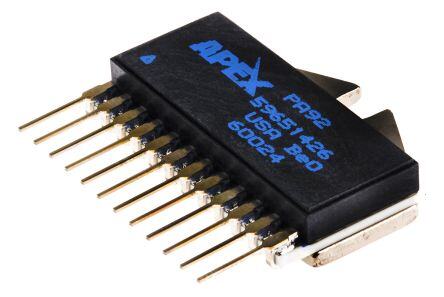
ICGOO电子元器件商城为您提供PA92由Apex Microtechnology Corporation设计生产,在icgoo商城现货销售,并且可以通过原厂、代理商等渠道进行代购。 PA92价格参考。Apex Microtechnology CorporationPA92封装/规格:线性 - 放大器 - 仪表,运算放大器,缓冲器放大器, 功率 放大器 1 电路 12-SIP。您可以下载PA92参考资料、Datasheet数据手册功能说明书,资料中有PA92 详细功能的应用电路图电压和使用方法及教程。
Apex Microtechnology的PA92是一款高性能、高精度的线性放大器,主要应用于工业和医疗设备中需要精确信号处理的场景。以下是其主要应用场景:

1. 精密测量与测试设备:
   PA92具有极低的噪声和高增益带宽积(GBW),适用于需要高精度测量的测试仪器。例如,在电子称重系统或高精度传感器中,PA92可以确保微弱信号被准确放大而不失真。

2. 医疗设备:
   在医疗领域,PA92可用于心电图(ECG)、脑电图(EEG)等生物电信号的放大。这些信号通常非常微弱且容易受到干扰,PA92的高共模抑制比(CMRR)和低输入偏置电流特性,能够有效提高信号质量,减少噪声影响。

3. 自动化控制系统:
   PA92在工业自动化控制中也有广泛应用。例如,在伺服控制系统中,它可以帮助精确控制电机的速度和位置,确保系统的稳定性和响应速度。此外,PA92还可以用于压力、温度等传感器信号的调理,提供稳定的输出信号给后续处理单元。

4. 音频处理设备:
   对于高端音频设备,如专业音响系统或录音设备,PA92的低失真和高线性度使其成为理想的音频信号放大器。它可以确保音频信号在整个频段内保持纯净,提供卓越的音质体验。

5. 通信系统:
   在通信领域,PA92可以用于射频(RF)前端模块中的信号放大。其宽频带特性和低噪声性能有助于提高通信系统的接收灵敏度和传输质量,特别适合于需要长距离传输的应用场景。

总之,PA92凭借其出色的电气性能和稳定性,广泛应用于对信号质量和可靠性要求极高的各种精密电子设备中。
| 参数 | 数值 |
| -3db带宽 | - |
| 产品目录 | 集成电路 (IC) |
| 描述 | IC OPAMP POWER 18MHZ 12SIP |
| 产品分类 | Linear - Amplifiers - Instrumentation, OP Amps, Buffer Amps |
| 品牌 | Apex Microtechnology |
| 数据手册 | |
| 产品图片 |
|
| 产品型号 | PA92 |
| rohs | 无铅 / 符合限制有害物质指令(RoHS)规范要求 |
| 产品系列 | Apex Precision Power® |
| 产品培训模块 | http://www.digikey.cn/PTM/IndividualPTM.page?site=cn&lang=zhs&ptm=30464 |
| 产品目录页面 | |
| 供应商器件封装 | 12-SIP |
| 其它名称 | 598-1332 |
| 包装 | 管件 |
| 压摆率 | 50 V/µs |
| 增益带宽积 | 18MHz |
| 安装类型 | 通孔 |
| 封装/外壳 | 12-SIP |
| 工作温度 | -25°C ~ 85°C |
| 应用说明 | |
| 放大器类型 | 功率 |
| 标准包装 | 1 |
| 特色产品 | http://www.digikey.com/product-highlights/cn/zh/apex-pa92h-hv-power-operational-amplifiers/3880 |
| 电压-电源,单/双 (±) | 100 V ~ 400 V, ±50 V ~ 200 V |
| 电压-输入失调 | 2mV |
| 电流-电源 | 10mA |
| 电流-输入偏置 | 200pA |
| 电流-输出/通道 | 4A |
| 电路数 | 1 |
| 输出类型 | - |
| 配用 | /product-detail/zh/EK16/598-1390-ND/1762014 |


- 商务部:美国ITC正式对集成电路等产品启动337调查
- 曝三星4nm工艺存在良率问题 高通将骁龙8 Gen1或转产台积电
- 太阳诱电将投资9.5亿元在常州建新厂生产MLCC 预计2023年完工
- 英特尔发布欧洲新工厂建设计划 深化IDM 2.0 战略
- 台积电先进制程称霸业界 有大客户加持明年业绩稳了
- 达到5530亿美元!SIA预计今年全球半导体销售额将创下新高
- 英特尔拟将自动驾驶子公司Mobileye上市 估值或超500亿美元
- 三星加码芯片和SET,合并消费电子和移动部门,撤换高东真等 CEO
- 三星电子宣布重大人事变动 还合并消费电子和移动部门
- 海关总署:前11个月进口集成电路产品价值2.52万亿元 增长14.8%


PDF Datasheet 数据手册内容提取
PA92 RoHS High Voltage Power Operational Amplifiers COMPLIANT FEATURES • High Voltage — 400V (±200V) • Low Quiescent Current — 10mA • High Output Current — 4A • Programmable Current Limit APPLICATIONS • Piezoelectric Positioning • High Voltage Instrumentation • Electrostatic Transducers • Programmable Power Supplies up to 390V DESCRIPTION The PA92 is a high voltage, low quiescent current MOSFET operational amplifier designed as a low cost solution for driving continuous output currents up to 4A and pulse currents up to 7A. The safe operating area (SOA) has no second breakdown limitations and can be observed for all type loads by choosing an appropri‐ ate current limiting resistor. The MOSFET output stage is biased AB for linear operation. External compensa‐ tion provides flexibility in choosing bandwidth and slew rate for the application. Apex Microtechnology’s Power SIP uses a minimum of board space allowing for high density circuit boards. The Power SIP is electri‐ cally isolated. Figure 1: Equivalent Schematic 12 11 +V S R1R2 C1 R3 Q3 Q1 Q2 R4 Q4 Q6 5 I CL 4 CC2 9 Q5 CC1 Q8 R7 10 Q14A Q14B Q11 1 6 –IN R5 R6 OUT Q13 R8 R9 Q12 3 2 IQ Q17 R10 +IN Q16 Q15 R11 R12 –V S 7 8 © Apex Microtechnology Inc. Oct 2018 www.apexanalog.com All rights reserved PA92U Rev S
PA92 TYPICAL CONNECTION Figure 2: Typical Connection R F 100 k +V S * 100nF R C C C R F +V S V + 1 k R OUT C PA92 C L C L -V S R L R CL -V *Bulk Bypass S Capacitors. Use 10μF per Amp of Output * 100nF Current. 2 PA92U Rev S
PA92 PINOUT AND DESCRIPTION TABLE Figure 3: External Connections Pin Number Name Description 1 ‐IN The inverting input. 2 +IN The non‐inverting input. Quiescent current reduction pin. Connect to pin 5 to disable the AB bias. See appli‐ 3 IQ cable section. Compensation resistor connection. Select value based on Phase Compensation. 4 RC See applicable section. Compensation capacitor connection. Select value based on Phase Compensation. 5 C C See applicable section. 6 OUT The output. Connect this pin to load and to the feedback resistors. 7, 8 ‐V The negative supply rail. Pins 7 and 8 are internally connected. S Connect to the current limit resistor. Output current flows into/out of these pins 9, 10 CL through R . The output pin and the load are connected to the other side of CL R .Pins 9 and 10 are internally connected. CL 11, 12 +V The positive supply rail. Pins 11 and 12 are internally connected. S PA92U Rev S 3
PA92 SPECIFICATIONS All Min/Max characteristics and specifications are guaranteed over the Specified Operating Conditions. Typical performance characteristics and specifications are derived from measurements taken at typical sup‐ ply voltages and T = 25°C. C ABSOLUTE MAXIMUM RATINGS Parameter Symbol Min Max Units Supply Voltage, total +V to ‐V 400 V S S Output Current, source, sink, peak, within SOA I 7 A OUT Power Dissipation, continuous @ T = 25°C P 80 W c D Input Voltage, differential V ‐20 20 V IN (Diff) Input Voltage, common mode V ‐V +V V CM S S Temperature, pin solder, 10s max. 260 °C Temperature, junction 1 TJ 150 °C Temperature Range, storage ‐55 +125 °C Operating Temperature Range, case T ‐40 +85 °C C 1. Long term operation at the maximum junction temperature will result in reduced product life. Derate power dissipation to achieve high MTTF. The PA92 is constructed from MOSFET transistors. ESD handling procedures must be observed. CAUTION The substrate contains beryllia (BeO). Do not crush, machine, or subject to temperatures in excess of 850°C to avoid generating toxic fumes. INPUT Parameter Test Conditions Min Typ Max Units Offset Voltage, initial 2 10 mV Offset Voltage vs. Temperature Full temp range 15 50 µV/°C Offset Voltage vs. Supply 10 25 µV/V Offset Voltage vs. Time 75 µV/kh Bias Current, initial 200 2000 pA Bias Current vs. Supply 4 pA/V Offset Current, initial 50 500 pA Input Impedance, DC 1011 Ω Input Capacitance 4 pF Common Mode Voltage Range 1 ±VS Ŧ 15 V Common Mode Rejection, DC V = ±90V 80 98 dB CM 100 kHz BW, R = 1 kΩ, S Noise 1 µV RMS C = 10pF C 1. +V and –V denote the positive and negative power supply rail respectively. S S 4 PA92U Rev S
PA92 GAIN Parameter Test Conditions Min Typ Max Units Open Loop @ 15 Hz R = 2 kΩ, C = 10pF 94 111 dB L C Gain Bandwidth Product @ 1 MHz R = 2 kΩ, C = 10pF 18 MHz L C Power Bandwidth R = 2 kΩ, C = 10pF 30 kHz L C Phase Margin Full temp range 60 ° OUTPUT Parameter Test Conditions Min Typ Max Units Voltage Swing 1 IOUT = 4A ±VS Ŧ 12 ±VS Ŧ 10 V Current, continuous 4 A Slew Rate, A = 100 C = 10pF 50 V/µs V C Capacitive Load, A = +1 Full temp range 1 nF V Settling Time to 0.1% C = 10pF, 2V step 1 µs C Resistance, no load 10 Ω 1. +V and –V denote the positive and negative power supply rail respectively. S S POWER SUPPLY Parameter Test Conditions Min Typ Max Units Voltage 1 ±50 ±150 ±200 V Current, quiescent 10 14 mA 1. Derate max supply rating 0.625 V/°C below 25°C case. No derating needed above 25°C case. THERMAL Parameter Test Conditions Min Typ Max Units Resistance, AC, junction to case 1 Full temp range, F > 60 Hz 1 °C/W Resistance, DC, junction to case Full temp range, F < 60 Hz 1.5 °C/W Resistance, junction to air Full temp range 30 °C/W temperature range, case Meets full range specs ‐25 +85 °C 1. Rating applies if the output current alternates between both output transistors at a rate faster than 60 Hz. PA92U Rev S 5
PA92 TYPICAL PERFORMANCE GRAPHS Figure 4: Power Derating Figure 5: Normalized Quiescent Current 80 1.6 ) ) (cid:116) (XQ (cid:87)(cid:3)(cid:894) t, I (cid:374)(cid:853)(cid:3) 60 en (cid:381) rr 1.4 (cid:415) u (cid:258) C (cid:393) t (cid:400)(cid:349) n (cid:24)(cid:349)(cid:400) 40 sce (cid:396)(cid:3) e (cid:286) ui (cid:449) Q (cid:87)(cid:381) d 1.2 (cid:258)(cid:367)(cid:3) 20 ze (cid:286)(cid:396)(cid:374) mali (cid:374)(cid:410) or (cid:47) N 0 1.0 0 25 50 75 100 125 25 50 75 100 125 Case Temperature, T (°C) Case Temperature, T (°C) C C Figure 6: Small Signal Response Figure 7: Phase Response 50 90 C = 150pF C 40 C = 100pF C ) C = 47pF B C 135 d C = 10pF ( C A 30 n, (cid:894)(cid:931)(cid:895) ai (cid:711)(cid:3) p G 20 e, 180 o as o h n L 10 P e C = 150pF p 225 C O C = 100pF C 0 C = 47pF C C = 10pF C -10 270 100k 1M 10M 100k 1M 10M Frequency, F (Hz) Frequency, F (Hz) 6 PA92U Rev S
PA92 Figure 8: Output Voltage Swing Figure 9: Power Response 8.5 400 ) V ( ) UT P-P O V V ( V- S 8.0 OUT V ply g, 100 p n u wi C = 10pF m S 7.5 e S C o g r a C = 47pF p F olt C o V Dr 7.0 ut C = 100pF e p C g ut a O t ol C = 150pF V C 6.5 10 0 1 2 3 4 1k 10k 100k 1M Output Current, I (A) Frequency, F (Hz) OUT Figure 10: Slew Rate Figure 11: Harmonic Distortion 60 0.1 40 P = 1W O P = 20W 30 O P = 62W O 20 (cid:895) (cid:400) (cid:895) (cid:645) (cid:1081) (cid:894)(cid:115)(cid:876) 10 (cid:374)(cid:3)(cid:894) e 8 (cid:381) 0.01 t (cid:415) Ra 6 (cid:381)(cid:396) w (cid:400)(cid:410) e 4 (cid:24)(cid:349) Sl 3 2 1 0.001 10 30 60 100 200 300 100 1k 10k (cid:28)(cid:454)(cid:410)(cid:856)(cid:3)(cid:18)(cid:381)(cid:373)(cid:393)(cid:286)(cid:374)(cid:400)(cid:258)(cid:415)(cid:381)(cid:374)(cid:3)(cid:18)(cid:258)(cid:393)(cid:258)(cid:272)(cid:349)(cid:410)(cid:381)(cid:396)(cid:853)(cid:3)(cid:18) (pF) Frequency, F (Hz) C PA92U Rev S 7
PA92 Figure 12: Input Noise Voltage Figure 13: Current Limit 20 4 (cid:460)(cid:895) 15 (cid:44) (cid:1103) (cid:115)(cid:876) 3 (cid:374) ) (cid:894) 10 A ge, V 7 t, I(CL ta mi 2 ol Li e V 5 nt s e oi rr N u t C 1 u p 3 n I 2 0 10 100 1k 10k 100k 0 0.2 0.4 0.6 0.8 1.0 1.2 Frequency, F (Hz) Resistor Value, R ((cid:591)) CL 8 PA92U Rev S
PA92 SAFE OPERATING AREA (SOA) The safe operating area curves define the maximum additional internal power dissipation the amplifier can tolerate when it produces the necessary output to drive an external load. The MOSFET output stage of this power operational amplifier has two distinct limitations: 1. The current handling capability of the MOSFET geometry and the wire bonds. 2. The junction temperature of the output MOSFETs. Note: The output stage is protected against transient flyback. However, for protection against sustained, high energy flyback, external fast‐recovery diodes should be used. Figure 14: SOA 8 DC, T = 25°C 6 ) C A 200 ms ( 4 S V (cid:882) (cid:396)(cid:3) 2 100 ms (cid:381) (cid:3) S V (cid:1085) T (cid:373)(cid:3) 0.18 C = 8 (cid:381) T 5°C (cid:396) C = (cid:38) 0.6 1 (cid:374)(cid:410)(cid:3) 0.4 25°C (cid:286) 0.3 (cid:396) (cid:396) (cid:437) 0.2 (cid:18) (cid:3) (cid:410) (cid:437) (cid:393) 0.1 (cid:410) (cid:437) 0.08 (cid:75) 0.06 0.04 10 20 30 40 6080100 200 300 500 (cid:94)(cid:437)(cid:393)(cid:393)(cid:367)(cid:455)(cid:3)(cid:410)(cid:381)(cid:3)(cid:75)(cid:437)(cid:410)(cid:393)(cid:437)(cid:410)(cid:3)(cid:24)(cid:349)(cid:299)(cid:286)(cid:396)(cid:286)(cid:374)(cid:415)(cid:258)(cid:367)(cid:853)(cid:3)V - V (V) S OUT PA92U Rev S 9
PA92 GENERAL Please read Application Note 1 “General Operating Considerations” which covers stability, supplies, heat sinking, mounting, current limit, SOA interpretation, and specification interpretation. Visit www.apexana‐ log.com for Apex Microtechnology’s complete Application Notes library, Technical Seminar Workbook, and Evaluation Kits. PHASE COMPENSATION Gain C * R C C ≥1 150pF 100 Ω ≥2 100pF 100 Ω ≥3 47pF 0 Ω ≥12 10pF 0 Ω *C Never to be <10pF. C to be rated for the full supply voltage +V to ‐V . Use ceramic NPO (COG) type. C C S S CURRENT LIMIT For proper operation, the current limit resistor (R ) must be connected as shown in the typical connec‐ CL tion diagram. For optimum reliability the resistor value should be set as high as possible. The value is calcu‐ lated as follows; with the maximum practical value of 16 Ω. 0.65V R = ----------------- CL I A CL INPUT PROTECTION Although the PA92 can withstand differential voltages up to ±20V, additional external protection is rec‐ ommended. Low leakage, low capacitance JFETs connected as diodes are recommended (e.g. 2N4416, Q1‐Q4 in Figure 15). The differential input voltage will be clamped to ±1.4V. This is sufficient overdrive to produce maximum power bandwidth. Figure 15: Overvoltage Protection 10 PA92U Rev S
PA92 POWER SUPPLY PROTECTION Unidirectional zener diode transient suppressors are recommended as protection on the supply pins. See Figure 315. The zeners clamp transients to voltages within the power supply rating and also clamp power sup‐ ply reversals to ground. Whether the zeners are used or not, the system power supply should be evaluated for transient performance including power‐on overshoot and power‐off polarity reversals as well as line regu‐ lation. Conditions which can cause open circuits or polarity reversals on either power supply rail should be avoided or protected against. Reversals or opens on the negative supply rail are known to induce input stage failure. Unidirectional transzorbs prevent this, and it is desirable that they be both electrically and physically as close to the amplifier as possible. STABILITY The PA92 is externally compensated and performance can be tailored to the application. Use the graphs of small signal response and power response as a guide. The compensation capacitor C must be rated at C 500V working voltage. An NPO capacitor is recommended. The compensation network C R must be C C mounted closely to the amplifier pins 4 and 5 to avoid spurious oscillation. QUIESCENT CURRENT REDUCTION When pin 3 (I ) is shorted to pin 5 (CC2) the AB biasing of the output stage is disabled. This lowers quies‐ Q cent power but also raises distortion since the output stage is then class C biased. The output stage bias cur‐ rent is nominally set at 1mA. Pin 3 may be left open if not used. PA92U Rev S 11
PA92 PACKAGE DESIGN Part Number Apex Package Style Description PA92 DP 12‐Pin SIP PA92EE EE 12‐Pin SIP w/ formed leads PACKAGE STYLE DP 12 PA92U Rev S
PA92 PACKAGE STYLE EE NEED TECHNICAL HELP? CONTACT APEX SUPPORT! For all Apex Microtechnology product questions and inquiries, call toll free 800-546-2739 in North America. For inquiries via email, please contact apex.support@apexanalog.com. International customers can also request support by contacting their local Apex Microtechnology Sales Representative. To find the one nearest to you, go to www.apexanalog.com IMPORTANT NOTICE Apex Microtechnology, Inc. has made every effort to insure the accuracy of the content contained in this document. However, the information is subject to change without notice and is provided "AS IS" without warranty of any kind (expressed or implied). Apex Microtechnology reserves the right to make changes without further notice to any specifications or products mentioned herein to improve reliability. This document is the property of Apex Microtechnology and by furnishing this information, Apex Microtechnology grants no license, expressed or implied under any patents, mask work rights, copyrights, trademarks, trade secrets or other intellectual property rights. Apex Microtechnology owns the copyrights associated with the information contained herein and gives consent for copies to be made of the information only for use within your organization with respect to Apex Microtechnology integrated circuits or other products of Apex Microtechnology. This consent does not extend to other copying such as copying for general distribution, advertising or promotional purposes, or for creating any work for resale. APEX MICROTECHNOLOGY PRODUCTS ARE NOT DESIGNED, AUTHORIZED OR WARRANTED TO BE SUITABLE FOR USE IN PRODUCTS USED FOR LIFE SUPPORT, AUTOMOTIVE SAFETY, SECURITY DEVICES, OR OTHER CRITICAL APPLICATIONS. PRODUCTS IN SUCH APPLICATIONS ARE UNDERSTOOD TO BE FULLY AT THE CUSTOMER OR THE CUSTOMER’S RISK. Apex Microtechnology, Apex and Apex Precision Power are trademarks of Apex Microtechnology, Inc. All other corporate names noted herein may be trademarks of their respective holders. PA92U Rev S 13