ICGOO在线商城 > 集成电路(IC) > 线性 - 放大器 - 仪表,运算放大器,缓冲器放大器 > MC33171DG
 Datasheet下载
- 型号: MC33171DG
- 制造商: ON Semiconductor
- 库位|库存: xxxx|xxxx
- 要求:
| 数量阶梯 | 香港交货 | 国内含税 |
| +xxxx | $xxxx | ¥xxxx |
查看当月历史价格
查看今年历史价格
MC33171DG产品简介:
ICGOO电子元器件商城为您提供MC33171DG由ON Semiconductor设计生产,在icgoo商城现货销售,并且可以通过原厂、代理商等渠道进行代购。 MC33171DG价格参考。ON SemiconductorMC33171DG封装/规格:线性 - 放大器 - 仪表,运算放大器,缓冲器放大器, 通用 放大器 1 电路 8-SOIC。您可以下载MC33171DG参考资料、Datasheet数据手册功能说明书,资料中有MC33171DG 详细功能的应用电路图电压和使用方法及教程。
MC33171DG是ON Semiconductor(安森美半导体)生产的一款线性放大器,属于仪表、运算及缓冲放大器类别。它是一款高精度、低功耗的双通道运算放大器,具有轨到轨输入输出特性,适用于多种应用场景,尤其在需要高精度和低噪声性能的场合表现优异。

 应用场景:

1. 工业自动化与控制:
   - 在工业控制系统中,MC33171DG可以用于传感器信号调理电路,如温度、压力、位移等传感器的信号放大。其高精度和低噪声特性确保了信号的准确性和稳定性,特别适合对精度要求较高的工业测量设备。

2. 医疗设备:
   - 该器件广泛应用于医疗电子设备中,如心电图机、血压计、血糖仪等。其低功耗和高精度特性使其非常适合用于便携式或电池供电的医疗设备,能够有效提高测量的准确性,减少误差。

3. 汽车电子:
   - 在汽车电子系统中,MC33171DG可用于车载传感器信号处理,如车速传感器、加速度传感器等。其轨到轨输入输出特性使得它能够在较宽的电压范围内工作,适应汽车电源系统的波动,同时保证信号的稳定传输。

4. 消费电子产品:
   - 在音频设备、智能家居控制器等消费电子产品中,MC33171DG可以用于音频信号放大或传感器信号处理。其低功耗特性有助于延长电池寿命,而高精度则确保了信号的质量。

5. 通信设备:
   - 在通信领域,MC33171DG可用于信号调理和放大,特别是在无线通信模块中,它可以用于射频前端的信号处理,提供稳定的信号增益,确保通信质量。

6. 测试与测量仪器:
   - 该器件也常用于各种测试与测量仪器中,如示波器、信号发生器等。其高精度和低噪声特性使其成为精密测量仪器的理想选择,能够提供更准确的测量结果。

总的来说,MC33171DG凭借其高精度、低功耗和轨到轨输入输出特性,适用于多种需要精确信号处理的应用场景,特别是在工业、医疗、汽车等领域表现出色。
| 参数 | 数值 |
| -3db带宽 | - |
| 产品目录 | 集成电路 (IC)半导体 |
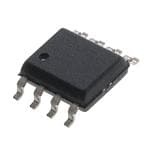
| 描述 | IC OPAMP GP 1.8MHZ 8SOIC运算放大器 - 运放 3-44V Single Lo PWR Industrial Temp |
| 产品分类 | Linear - Amplifiers - Instrumentation, OP Amps, Buffer Amps集成电路 - IC |
| 品牌 | ON Semiconductor |
| 产品手册 | |
| 产品图片 |
|
| rohs | 符合RoHS无铅 / 符合限制有害物质指令(RoHS)规范要求 |
| 产品系列 | 放大器 IC,运算放大器 - 运放,ON Semiconductor MC33171DG- |
| 数据手册 | |
| 产品型号 | MC33171DG |
| 产品目录页面 | |
| 产品种类 | 运算放大器 - 运放 |
| 供应商器件封装 | 8-SOIC N |
| 共模抑制比—最小值 | 80 dB |
| 关闭 | No Shutdown |
| 其它名称 | MC33171DGOS |
| 包装 | 管件 |
| 压摆率 | 2.1 V/µs |
| 双重电源电压 | +/- 3 V, +/- 5 V, +/- 9 V |
| 商标 | ON Semiconductor |
| 增益带宽生成 | 1.8 MHz |
| 增益带宽积 | 1.8MHz |
| 安装类型 | 表面贴装 |
| 安装风格 | SMD/SMT |
| 封装 | Tube |
| 封装/外壳 | 8-SOIC(0.154",3.90mm 宽) |
| 封装/箱体 | SOIC-8 |
| 工作温度 | -40°C ~ 85°C |
| 工作电源电压 | 3 V to 44 V, +/- 1.5 V to +/- 22 V |
| 工厂包装数量 | 98 |
| 技术 | Bipolar |
| 放大器类型 | 通用 |
| 最大双重电源电压 | +/- 22 V |
| 最大工作温度 | + 85 C |
| 最小双重电源电压 | +/- 1.5 V |
| 最小工作温度 | - 40 C |
| 标准包装 | 98 |
| 电压-电源,单/双 (±) | 3 V ~ 44 V, ±1.5 V ~ 22 V |
| 电压-输入失调 | 2mV |
| 电流-电源 | 220µA |
| 电流-输入偏置 | 20nA |
| 电流-输出/通道 | 27mA |
| 电源电流 | 0.22 mA |
| 电路数 | 1 |
| 系列 | MC33171 |
| 转换速度 | 2.1 V/us |
| 输入偏压电流—最大 | 100 nA |
| 输入参考电压噪声 | 32 nV |
| 输入补偿电压 | 5 mV |
| 输出电流 | 5 mA |
| 输出类型 | - |
| 通道数量 | 1 Channel |


PDF Datasheet 数据手册内容提取
MC33171, 2, 4, NCV33172, 4 Single Supply 3.0 V to 44 V, Low Power Operational Amplifiers www.onsemi.com Quality bipolar fabrication with innovative design concepts are employed for the MC33171/72/74, NCV33172/74 series of monolithic operational amplifiers. These devices operate at 180(cid:2)A per amplifier and offer 1.8 MHz of gain bandwidth product and PDIP−8 2.1V/(cid:2)s slew rate without the use of JFET device technology. P SUFFIX Although this series can be operated from split supplies, it is CASE 626 8 particularly suited for single supply operation, since the common 1 mode input voltage includes ground potential (V ). With a EE Darlington input stage, these devices exhibit high input resistance, low SO−8 input offset voltage and high gain. The all NPN output stage, D, VD SUFFIX 8 CASE 751 characterized by no deadband crossover distortion and large output 1 voltage swing, provides high capacitance drive capability, excellent phase and gain margins, low open loop high frequency output impedance and symmetrical source/sink AC frequency response. The MC33171/72/74, NCV33172/74 are specified over the PDIP−14 industrial/automotive temperature ranges. The complete series of P, VP SUFFIX single, dual and quad operational amplifiers are available in plastic as CASE 646 well as the surface mount packages. 14 1 Features SO−14 • Low Supply Current: 180 (cid:2)A (Per Amplifier) 14 D, VD SUFFIX • Wide Supply Operating Range: 3.0 V to 44 V or ±1.5 V to ±22 V CASE 751A 1 • Wide Input Common Mode Range, Including Ground (V ) EE • Wide Bandwidth: 1.8 MHz TSSOP−14 • High Slew Rate: 2.1 V/(cid:2)s 14 DTB SUFFIX CASE 948G • 1 Low Input Offset Voltage: 2.0 mV • Large Output Voltage Swing: −14.2 V to +14.2 V (with ±15 V Supplies) ORDERING INFORMATION • See detailed ordering and shipping information in the package Large Capacitance Drive Capability: 0 pF to 500 pF dimensions section on page 9 of this data sheet. • Low Total Harmonic Distortion: 0.03% • Excellent Phase Margin: 60° • DEVICE MARKING INFORMATION Excellent Gain Margin: 15 dB See general marking information in the device marking • Output Short Circuit Protection section on page 10 of this data sheet. • ESD Diodes Provide Input Protection for Dual and Quad • NCV Prefix for Automotive and Other Applications Requiring Unique Site and Control Change Requirements; AEC−Q100 Qualified and PPAP Capable • These Devices are Pb−Free, Halogen Free/BFR Free and are RoHS Compliant © Semiconductor Components Industries, LLC, 2015 1 Publication Order Number: May, 2015 − Rev. 13 MC33171/D
MC33171, 2, 4, NCV33172, 4 PIN CONNECTIONS SINGLE QUAD Offset Null 1 8 NC Output 1 1 14 Output 4 NonIinnvv.. IInnppuutt 23 +- 76 VOCuCtput Inputs 1 23 -+ 1 4 -+ 1123 Inputs 4 VEE 4 5 Offset Null VCC 4 11 VEE (Single, Top View) 5 + + 10 Inputs 2 2 3 Inputs 3 - - 6 9 Output 2 7 8 Output 3 DUAL (Top View) Output 1 1 8 VCC Inputs 1 2 - 1 7 Output 2 + 3 2 - 6 Inputs 2 + VEE 4 5 (Top View) VCC Q3 Q4 Q5 Q6 Q7 Q1 Q17 Q2 R1 C1 R2 D2 Bias Q18 - Q8 Q9 Q10 Q11 R6 R7 Output Inputs R8 + C2 D3 Q19 Q13 Q14 Q15 Q16 Q12 Current D1 Limit R5 R3 R4 VEE/GND Offset Null (MC33171) Figure 1. Representative Schematic Diagram (Each Amplifier) www.onsemi.com 2
MC33171, 2, 4, NCV33172, 4 MAXIMUM RATINGS Rating Symbol Value Unit Supply Voltage VCC/VEE ±22 V Input Differential Voltage Range VIDR (Note 1) V Input Voltage Range VIR (Note 1) V Output Short Circuit Duration (Note 2) tSC Indefinite sec Operating Ambient Temperature Range TA (Note 3) °C Operating Junction Temperature TJ +150 °C Storage Temperature Range Tstg −65 to +150 °C Stresses exceeding those listed in the Maximum Ratings table may damage the device. If any of these limits are exceeded, device functionality should not be assumed, damage may occur and reliability may be affected. DC ELECTRICAL CHARACTERISTICS (VCC = +15 V, VEE = −15 V, RL connected to ground, TA = +25°C, unless otherwise noted.) Characteristics Symbol Min Typ Max Unit Input Offset Voltage (VCM = 0 V) VIO mV VCC = +15 V, VEE = −15 V, TA = +25°C − 2.0 4.5 VCC = +5.0 V, VEE = 0 V, TA = +25°C − 2.5 5.0 VCC = +15 V, VEE = −15 V, TA = Tlow to Thigh (Note 3) − − 6.5 Average Temperature Coefficient of Offset Voltage (cid:3)VIO/(cid:3)T − 10 − (cid:2)V/°C Input Bias Current (VCM = 0 V) IIB nA TA = +25°C − 20 100 TA = Tlow to Thigh (Note 3) − − 200 Input Offset Current (VCM = 0 V) IIO nA TA = +25°C − 5.0 20 TA = Tlow to Thigh (Note 3) − − 40 Large Signal Voltage Gain (VO = ±10 V, RL = 10 k) AVOL V/mV TA = +25°C 50 500 − TA = Tlow to Thigh (Note 3) 25 − − Output Voltage Swing VOH V VCC = +5.0 V, VEE = 0 V, RL = 10 k, TA = +25°C 3.5 4.3 − VCC = +15 V, VEE = −15 V, RL = 10 k, TA = +25°C 13.6 14.2 − VCC = +15 V, VEE = −15 V, RL = 10 k, TA = Tlow to Thigh (Note 3) 13.3 − − VCC = +5.0 V, VEE = 0 V, RL = 10 k, TA = +25°C VOL − 0.05 0.15 VCC = +15 V, VEE = −15 V, RL = 10 k, TA = +25°C − −14.2 −13.6 VCC = +15 V, VEE = −15 V, RL = 10 k, TA = Tlow to Thigh (Note 3) − − −13.3 Output Short Circuit (TA = +25°C) ISC mA Input Overdrive = 1.0 V, Output to Ground Source 3.0 5.0 − Sink 15 27 − Input Common Mode Voltage Range VICR V TA = +25°C VEE to (VCC −1.8) TA = Tlow to Thigh (Note 3) VEE to (VCC −2.2) Common Mode Rejection Ratio (RS ≤ 10 k), TA = +25°C CMRR 80 90 − dB Power Supply Rejection Ratio (RS = 100 (cid:4)), TA = +25°C PSRR 80 100 − dB Power Supply Current (Per Amplifier) ID (cid:2)A VCC = +5.0 V, VEE = 0 V, TA = +25°C − 180 250 VCC = +15 V, VEE = −15 V, TA = +25°C − 220 250 VCC = +15 V, VEE = −15 V, TA = Tlow to Thigh (Note 3) − − 300 1. Either or both input voltages must not exceed the magnitude of VCC or VEE. 2. Power dissipation must be considered to ensure maximum junction temperature (TJ) is not exceeded. 3. MC3317x Tlow = −40°C Thigh = +85°C MC3317xV, NCV3317x Tlow = −40°C Thigh = +125°C www.onsemi.com 3
MC33171, 2, 4, NCV33172, 4 AC ELECTRICAL CHARACTERISTICS (VCC = +15 V, VEE = −15 V, RL connected to ground, TA = +25°C, unless otherwise noted.) Characteristics Symbol Min Typ Max Unit Slew Rate (Vin = −10 V to +10 V, RL = 10 k, CL = 100 pF) SR V/(cid:2)s AV +1 1.6 2.1 − AV −1 − 2.1 − Gain Bandwidth Product (f = 100 kHz) GBW 1.4 1.8 − MHz Power Bandwidth BWp kHz AV = +1.0 RL = 10 k, VO = 20 Vpp, THD = 5% − 35 − Phase Margin (cid:5) Deg m RL = 10 k − 60 − RL = 10 k, CL = 100 pF − 45 − Gain Margin Am dB RL = 10 k − 15 − RL = 10 k, CL = 100 pF − 5.0 − Equivalent Input Noise Voltage en − 32 − nV/√Hz RS = 100 (cid:4), f = 1.0 kHz Equivalent Input Noise Current (f = 1.0 kHz) In − 0.2 − pA/√Hz Differential Input Resistance Rin M(cid:4) Vcm = 0 V − 300 − Input Capacitance Cin − 0.8 − pF Total Harmonic Distortion THD % AV = +10, RL = 10 k, 2.0 Vpp ≤ VO ≤ 20 Vpp, f = 10 kHz − 0.03 − Channel Separation (f = 10 kHz) CS − 120 − dB Open Loop Output Impedance (f = 1.0 MHz) zo − 100 − (cid:4) Product parametric performance is indicated in the Electrical Characteristics for the listed test conditions, unless otherwise noted. Product performance may not be indicated by the Electrical Characteristics if operated under different conditions. NGE (V) 0 VCC VCC/V(cid:3)EEV =IO ± =1 .55. 0V m toV ±22 V GE (V) 0 VCC VCC/VEE T=A ± =5 2.05 °VC to ±22 V A-0.8 A E R OLT -1.0 Source G V LTA-1.6 ON E VO RATI D U ON MO -2.4 UT SAT 1.0 M P M 0.1 T UT CO VEE (cid:2)(cid:3), OUat Sink VEE P 0 Vs 0 N -55 -25 0 25 50 75 100 125 0 1.0 2.0 3.0 4.0 (cid:2) , ICR TA, AMBIENT TEMPERATURE (°C) IL, LOAD CURRENT (±mA) VI Figure 2. Input Common Mode Voltage Range Figure 3. Split Supply Output Saturation versus Temperature versus Load Current www.onsemi.com 4
MC33171, 2, 4, NCV33172, 4 B) 3 70 70 N (d 0 120 S)60 60 , OPEN LOOP VOLTAGE GAIVOL--211200000 VRVT123A oCL---u C= =tPPG / = V21hha E50aa0inE° ss kVC ee=, ±C1L 5= V 100 pF MP=ha 5ar8gs°ien 23 14 =M G1a5arg indinB 111224680200000φ, EXCESS PAHSE (DEGREES) φm, PHASE MARGIN (DEGREE5432100000 (cid:5)%m VAR(cid:3)TAVCLV O C==OL/ V 21==E50 2E°+ kC0 1 = .m0 V±p1p5 V 5432100000%, PERCENT OVERSHOOT A -30 4 - Gain, CL = 100 pF 0 0 100 k 1.0 M 10 M 10 20 50 100 200 500 1.0 k f, FREQUENCY (Hz) CL, LOAD CAPACITANCE (pF) Figure 4. Open Loop Voltage Gain and Figure 5. Phase Margin and Percent Phase versus Frequency Overshoot versus Load Capacitance 5.0 (cid:2)s/DIV 1.3 R (NORMALIZED) 111...210 GBW VRCL C=/ V1E0E k = ±15 V 50 mV/DIV0 VVV(cid:3)TACCOI OCM == / =V =20 E5 ± 0VE°0 C V.=5 ±m1A5 V S SR D N 0.9 A W B V G 0.8 DI V/0 0 1 0.7 -55 -25 0 25 50 75 100 12 5 TA, AMBIENT TEMPERATURE (°C) 5.0 (cid:2)s/DIV Figure 6. Normalized Gain Bandwidth Product Figure 7. Small and Large Signal and Slew Rate versus Temperature Transient Response 140 1.1 VCC/VEE = ±15 V mA) 1. TA = -55°C 1 Ω(cid:2))120 ARVL == +101 .k0 AV = 1000 ENT ( 0.9 23.. TTAA == 1 2255°°CC Quad 2 E (100 CL = 100 pF RR 3 ANC TA = 25°C AV = 100 Y CU 0.7 D 80 L E P P P M U Dual 1 OUTPUT I 6400 AV = 10 AV = 1.0 POWER S 0.5 23 z(cid:4) , o 20 (cid:2)(cid:4), CC 0.3 Single 12 (cid:2), ID 3 0 I 0.1 200 2.0 k 20 k 200 k 2.0 M 0 5.0 10 15 20 25 f, FREQUENCY (Hz) VCC/VEE, SUPPLY VOLTAGE (±V) Figure 8. Output Impedance and Frequency Figure 9. Supply Current versus Supply Voltage www.onsemi.com 5
MC33171, 2, 4, NCV33172, 4 APPLICATIONS INFORMATION − CIRCUIT DESCRIPTION/PERFORMANCE FEATURES Although the bandwidth, slew rate, and settling time of the 0.8V of the positive rail (V ) and negative rail (V ), CC EE MC33171/72/74 amplifier family is similar to low power op providing a 28.4 Vpp swing from ±15 V supplies. This large amp products utilizing JFET input devices, these amplifiers output swing becomes most noticeable at lower supply offer additional advantages as a result of the PNP transistor voltages. differential inputs and an all NPN transistor output stage. The positive swing is limited by the saturation voltage of Because the input common mode voltage range of this the current source transistor Q7, the V of the NPN pull−up BE input stage includes the V potential, single supply transistor Q17, and the voltage drop associated with the EE operation is feasible to as low as 3.0 V with the common short circuit resistance, R5. For sink currents less than mode input voltage at ground potential. 0.4 mA, the negative swing is limited by the saturation The input stage also allows differential input voltages up voltage of the pull−down transistor Q15, and the voltage to ±44 V, provided the maximum input voltage range is not drop across R4 and R5. For small valued sink currents, the exceeded. Specifically, the input voltages must range above voltage drops are negligible, allowing the negative between V and V supply voltages as shown by the swing voltage to approach within millivolts of V . For sink CC EE EE maximum rating table. In practice, although not currents (> 0.4 mA), diode D3 clamps the voltage across R4. recommended, the input voltages can exceed the V Thus the negative swing is limited by the saturation voltage CC voltage by approximately 3.0 V and decrease below the V of Q15, plus the forward diode drop of D3 (≈V +1.0 V). EE EE voltage by 0.3 V without causing product damage, although Therefore an unprecedented peak−to−peak output voltage output phase reversal may occur. It is also possible to source swing is possible for a given supply voltage as indicated by up to 5.0 mA of current from V through either inputs’ the output swing specifications. EE clamping diode without damage or latching, but phase If the load resistance is referenced to V instead of CC reversal may again occur. If at least one input is within the ground for single supply applications, the maximum common mode input voltage range and the other input is possible output swing can be achieved for a given supply within the maximum input voltage range, no phase reversal voltage. For light load currents, the load resistance will pull will occur. If both inputs exceed the upper common mode the output to V during the positive swing and the output CC input voltage limit, the output will be forced to its lowest will pull the load resistance near ground during the negative voltage state. swing. The load resistance value should be much less than Since the input capacitance associated with the small that of the feedback resistance to maximize pull−up geometry input device is substantially lower (0.8 pF) than capability. that of a typical JFET (3.0 pF), the frequency response for Because the PNP output emitter−follower transistor has a given input source resistance is greatly enhanced. This been eliminated, the MC33171/72/74 family offers a 15 mA becomes evident in D−to−A current to voltage conversion minimum current sink capability, typically to an output applications where the feedback resistance can form a pole voltage of (V +1.8 V). In single supply applications the EE with the input capacitance of the op amp. This input pole output can directly source or sink base current from a creates a 2nd Order system with the single pole op amp and common emitter NPN transistor for current switching is therefore detrimental to its settling time. In this context, applications. lower input capacitance is desirable especially for higher In addition, the all NPN transistor output stage is values of feedback resistances (lower current DACs). This inherently faster than PNP types, contributing to the bipolar input pole can be compensated for by creating a feedback amplifier’s improved gain bandwidth product. The zero with a capacitance across the feedback resistance, if associated high frequency low output impedance (200(cid:4) typ necessary, to reduce overshoot. For 10 k(cid:4) of feedback @ 1.0MHz) allows capacitive drive capability from 0 pF to resistance, the MC33171/72/74 family can typically settle to 400 pF without oscillation in the noninverting unity gain within 1/2 LSB of 8 bits in 4.2 (cid:2)s, and within 1/2 LSB of 12 configuration. The 60° phase margin and 15 dB gain margin, bits in 4.8 (cid:2)s for a 10V step. In a standard inverting unity as well as the general gain and phase characteristics, are gain fast settling configuration, the symmetrical slew rate is virtually independent of the source/sink output swing typically ±2.1 V/(cid:2)s. In the classic noninverting unity gain conditions. This allows easier system phase compensation, configuration the typical output positive slew rate is also since output swing will not be a phase consideration. The AC 2.1V/(cid:2)s, and the corresponding negative slew rate will characteristics of the MC33171/72/74 family also allow usually exceed the positive slew rate as a function of the fall excellent active filter capability, especially for low voltage time of the input waveform. single supply applications. The all NPN output stage, shown in its basic form on the Although the single supply specification is defined at equivalent circuit schematic, offers unique advantages over 5.0 V, these amplifiers are functional to at least 3.0V @ the more conventional NPN/PNP transistor Class AB output 25°C. However slight changes in parametrics such as stage. A 10 k(cid:4) load resistance can typically swing within bandwidth, slew rate, and DC gain may occur. www.onsemi.com 6
MC33171, 2, 4, NCV33172, 4 If power to this integrated circuit is applied in reverse pole for optimum frequency response, but also minimizes polarity, or if the IC is installed backwards in a socket, large extraneous “pick up” at this node. Supply decoupling with unlimited current surges will occur through the device that adequate capacitance immediately adjacent to the supply pin may result in device destruction. is also important, particularly over temperature, since many As usual with most high frequency amplifiers, proper lead types of decoupling capacitors exhibit great impedance dress, component placement and PC board layout should be changes over temperature. exercised for optimum frequency performance. For The output of any one amplifier is current limited and thus example, long unshielded input or output leads may result in protected from a direct short to ground. However, under unwanted input/output coupling. In order to preserve the such conditions, it is important not to allow the device to relatively low input capacitance associated with these exceed the maximum junction temperature rating. Typically amplifiers, resistors connected to the inputs should be for ±15 V supplies, any one output can be shorted immediately adjacent to the input pin to minimize additional continuously to ground without exceeding the maximum stray input capacitance. This not only minimizes the input temperature rating. www.onsemi.com 7
MC33171, 2, 4, NCV33172, 4 VCC 2.2 k 510 k VCC 100 k VO 0 3.6 Vpp 100 k VO 0 3.8 Vpp Cin + CO VO 100 k + CO - 10 k - VO Vin 100 k RL 100 k Cin 10 k RL 100 k 1.0 k Vin AV = 101 AV = 10 BW ( -3.0 dB) = 20 kHz BW ( -3.0 dB) = 200 kHz Figure 10. AC Coupled Noninverting Amplifier Figure 11. AC Coupled Inverting Amplifier with Single +5.0 V Supply with Single +5.0 V Supply 100 k VCC VCC 50 k 3 7 4.7 k + RL + 6 VO 2 - 5 - 1 4 10 k 100 k 1.0 M Vin VO 2.5 V 4.2 Vpp VEE Offset Nulling range is approximately ±80 mV with AV = 10 a 10 k potentiometer, MC33171 only. BW ( -3.0 dB) = 200 kHz Figure 12. DC Coupled Inverting Amplifier Figure 13. Offset Nulling Circuit Maximum Output Swing with Single +5.0 V Supply Vin ≥ 0.2 Vdc VfoC =C 30 kHz 16 k 16 k - VO R1 0.0C47 R2.32 k QHO = = 1 01.0 Vin 0R.01 C R + Vin 1.1 k C - VO + 0.047 R2 5.6 k 2C 2R 2C fo = 1.0 kHz 0.4 0.02 32 k 0.02 fo = 4 p1 RC VCC Then: R1 =2 RH3O R2 = 4QR2R11 R -3R3 Given fo = center frequency R3 = Q Qo fo < 0.1 Ao = Gain at center frequency (cid:6) foC GBW Choose Value fo, Q, Ao, C For less than 10% error for operational amplifier, where fo and GBW are expressed in Hz. Figure 14. Active High−Q Notch Filter Figure 15. Active Bandpass Filter www.onsemi.com 8
MC33171, 2, 4, NCV33172, 4 ORDERING INFORMATION Op Amp Operating Function Device Temperature Range Package Shipping† MC33171DG SO−8 98 Units/Rail (Pb−Free) MC33171DR2G SO−8 Single TA = −40° to +85°C (Pb−Free) 2500 / Tape & Reel MC33171PG PDIP 50 Units/Rail (Pb−Free) MC33172DG SO−8 98 Units/Rail (Pb−Free) MC33172DR2G SO−8 TA = −40° to +85°C (Pb−Free) 2500 / Tape & Reel MC33172PG PDIP 50 Units/Rail (Pb−Free) Dual MC33172VDG SO−8 98 Units/Rail (Pb−Free) MC33172VDR2G SO−8 TA = −40° to +125°C (Pb−Free) 2500 / Tape & Reel SO−8 NCV33172DR2G* 2500 / Tape & Reel (Pb−Free) MC33174DG SO−14 55 Units/Rail (Pb−Free) MC33174DR2G SO−14 2500 / Tape & Reel (Pb−Free) MC33174DTBG TSSOP−14 TA = −40° to +85°C (Pb−Free) 96 Units/Rail MC33174DTBR2G TSSOP−14 2500 / Tape & Reel (Pb−Free) MC33174PG PDIP Quad 25 Units/Rail (Pb−Free) MC33174VDG SO−14 55 Units/Rail (Pb−Free) MC33174VDR2G SO−14 2500 / Tape & Reel (Pb−Free) TA = −40° to +125°C MC33174VPG PDIP 25 Units/Rail (Pb−Free) NCV33174DTBR2G* TSSOP−14 2500 / Tape & Reel (Pb−Free) †For information on tape and reel specifications, including part orientation and tape sizes, please refer to our Tape and Reel Packaging Specifications Brochure, BRD8011/D. *NCV prefix for automotive and other applications requiring site and change controls. www.onsemi.com 9
MC33171, 2, 4, NCV33172, 4 MARKING DIAGRAMS SO−8 PDIP−8 SO−8 MC33172VD P SUFFIX D SUFFIX NCV33172D CASE 626 CASE 751 CASE 751 8 8 8 MC3317xP 3317x 3172V AWL ALYW ALYW (cid:2) (cid:2) YYWWG 1 1 1 PDIP−14 PDIP−14 SO−14 SO−14 P SUFFIX VP SUFFIX D SUFFIX VD SUFFIX CASE 646 CASE 646 CASE 751A CASE 751A 14 14 14 14 MC33174P MC33174VP MC33174DG MC33174VDG AWLYYWWG AWLYYWWG AWLYWW AWLYWW 1 1 1 1 TSSOP−14 TSSOP−14 MC33174 NCV33174 CASE 948G CASE 948G 14 14 MC33 NCV3 174 3174 ALYW(cid:2) ALYW(cid:2) (cid:2) (cid:2) 1 1 x = 1 or 2 A = Assembly Location WL, L = Wafer Lot YY, Y = Year WW, W = Work Week G or (cid:2) = Pb−Free Package (Note: Microdot may be in either location) www.onsemi.com 10
MC33171, 2, 4, NCV33172, 4 PACKAGE DIMENSIONS 8 LEAD PDIP CASE 626−05 ISSUE M NOTES: D A 1. DIMENSIONING AND TOLERANCING PER ASME Y14.5M, 1994. D1 2. CONTROLLING DIMENSION: INCHES. 3. DIMENSION E IS MEASURED WITH THE LEADS RE- E STRAINED PARALLEL AT WIDTH E2. 4. DIMENSION E1 DOES NOT INCLUDE MOLD FLASH. 8 5 5. ROUNDED CORNERS OPTIONAL. E1 INCHES MILLIMETERS DIM MIN NOM MAX MIN NOM MAX A −−−− −−−− 0.210 −−−− −−−− 5.33 1 4 A1 0.015 −−−− −−−− 0.38 −−−− −−−− b 0.014 0.018 0.022 0.35 0.46 0.56 C 0.008 0.010 0.014 0.20 0.25 0.36 NOTE 5 F c D 0.355 0.365 0.400 9.02 9.27 10.02 D1 0.005 −−−− −−−− 0.13 −−−− −−−− TOP VIEW E2 E 0.300 0.310 0.325 7.62 7.87 8.26 E1 0.240 0.250 0.280 6.10 6.35 7.11 END VIEW E2 0.300 BSC 7.62 BSC NOTE 3 E3 −−−− −−−− 0.430 −−−− −−−− 10.92 e 0.100 BSC 2.54 BSC e/2 A L 0.115 0.130 0.150 2.92 3.30 3.81 L A1 C SEATING PLANE E3 e 8Xb 0.010 M C A SIDE VIEW END VIEW www.onsemi.com 11
MC33171, 2, 4, NCV33172, 4 PACKAGE DIMENSIONS SOIC−8 NB CASE 751−07 ISSUE AK NOTES: −X− 1. DIMENSIONING AND TOLERANCING PER ANSI Y14.5M, 1982. A 2. CONTROLLING DIMENSION: MILLIMETER. 3. DIMENSION A AND B DO NOT INCLUDE MOLD PROTRUSION. 4. MAXIMUM MOLD PROTRUSION 0.15 (0.006) 8 5 PER SIDE. 5. DIMENSION D DOES NOT INCLUDE DAMBAR B S 0.25 (0.010) M Y M PROTRUSION. ALLOWABLE DAMBAR PROTRUSION SHALL BE 0.127 (0.005) TOTAL 1 IN EXCESS OF THE D DIMENSION AT −Y− 4 K 6. 7M5A1X−I0M1U TMH RMUA T7E51R−IA0L6 CAROEN DOIBTSIOONL.ETE. NEW STANDARD IS 751−07. G MILLIMETERS INCHES DIM MIN MAX MIN MAX A 4.80 5.00 0.189 0.197 C NX 45(cid:3) B 3.80 4.00 0.150 0.157 SEATING C 1.35 1.75 0.053 0.069 PLANE D 0.33 0.51 0.013 0.020 −Z− G 1.27 BSC 0.050 BSC H 0.10 0.25 0.004 0.010 0.10 (0.004) J 0.19 0.25 0.007 0.010 H D M J K 0.40 1.27 0.016 0.050 M 0 (cid:3) 8 (cid:3) 0 (cid:3) 8 (cid:3) N 0.25 0.50 0.010 0.020 0.25 (0.010)M Z Y S X S S 5.80 6.20 0.228 0.244 SOLDERING FOOTPRINT* 1.52 0.060 7.0 4.0 0.275 0.155 0.6 1.270 0.024 0.050 (cid:2) (cid:3) mm SCALE 6:1 inches *For additional information on our Pb−Free strategy and soldering details, please download the ON Semiconductor Soldering and Mounting Techniques Reference Manual, SOLDERRM/D. www.onsemi.com 12
MC33171, 2, 4, NCV33172, 4 PACKAGE DIMENSIONS PDIP−14 CASE 646−06 ISSUE P NOTES: 1. DIMENSIONING AND TOLERANCING PER ANSI Y14.5M, 1982. 14 8 2. CONTROLLING DIMENSION: INCH. 3. DIMENSION L TO CENTER OF LEADS WHEN B FORMED PARALLEL. 4. DIMENSION B DOES NOT INCLUDE MOLD FLASH. 1 7 5. ROUNDED CORNERS OPTIONAL. INCHES MILLIMETERS A DIM MIN MAX MIN MAX A 0.715 0.770 18.16 19.56 F L B 0.240 0.260 6.10 6.60 C 0.145 0.185 3.69 4.69 D 0.015 0.021 0.38 0.53 N C GF 0.004.1000 B0S.0C70 1.20.254 BS1C.78 H 0.052 0.095 1.32 2.41 −T− J 0.008 0.015 0.20 0.38 K 0.115 0.135 2.92 3.43 SEATING L 0.290 0.310 7.37 7.87 PLANE K J M −−− 10 (cid:3) −−− 10 (cid:3) H G D14 PL M N 0.015 0.039 0.38 1.01 0.13 (0.005) M www.onsemi.com 13
MC33171, 2, 4, NCV33172, 4 PACKAGE DIMENSIONS SOIC−14 CASE 751A−03 ISSUE J NOTES: 1.DIMENSIONING AND TOLERANCING PER −A− ANSI Y14.5M, 1982. 2.CONTROLLING DIMENSION: MILLIMETER. 14 8 3.DIMENSIONS A AND B DO NOT INCLUDE MOLD PROTRUSION. 4.MAXIMUM MOLD PROTRUSION 0.15 (0.006) PER SIDE. −B− P7 PL 5.DDIAMMEBNASRIO PNR DO TDROUESSIO NNO. TA LINLCOLWUADBELE 0.25 (0.010) M B M DAMBAR PROTRUSION SHALL BE 0.127 (0.005) TOTAL IN EXCESS OF THE D DIMENSION AT MAXIMUM MATERIAL 1 7 CONDITION. G MILLIMETERS INCHES RX 45(cid:3) F DIM MIN MAX MIN MAX C A 8.55 8.75 0.337 0.344 B 3.80 4.00 0.150 0.157 C 1.35 1.75 0.054 0.068 −T− D 0.35 0.49 0.014 0.019 SEATING D14 PL K M J GF 0.14.027 BS1C.25 0.001.0650 B0.S0C49 PLANE J 0.19 0.25 0.008 0.009 0.25 (0.010) M T B S A S K 0.10 0.25 0.004 0.009 M 0 (cid:3) 7 (cid:3) 0 (cid:3) 7 (cid:3) P 5.80 6.20 0.228 0.244 R 0.25 0.50 0.010 0.019 SOLDERING FOOTPRINT 7X 7.04 14X 1.52 1 14X 0.58 1.27 PITCH DIMENSIONS: MILLIMETERS *For additional information on our Pb−Free strategy and soldering details, please download the ON Semiconductor Soldering and Mounting Techniques Reference Manual, SOLDERRM/D. www.onsemi.com 14
MC33171, 2, 4, NCV33172, 4 PACKAGE DIMENSIONS TSSOP−14 CASE 948G ISSUE B NOTES: 1. DIMENSIONING AND TOLERANCING PER 14X K REF ANSI Y14.5M, 1982. 2. CONTROLLING DIMENSION: MILLIMETER. 0.10 (0.004) M T U S V S 3. DIMENSION A DOES NOT INCLUDE MOLD FLASH, PROTRUSIONS OR GATE BURRS. 0.15 (0.006) T U S MOLD FLASH OR GATE BURRS SHALL NOT EXCEED 0.15 (0.006) PER SIDE. N 4. DIMENSION B DOES NOT INCLUDE 0.25 (0.010) INTERLEAD FLASH OR PROTRUSION. 2XL/2 14 8 INTERLEAD FLASH OR PROTRUSION SHALL NOT EXCEED 0.25 (0.010) PER SIDE. M 5. DIMENSION K DOES NOT INCLUDE DAMBAR PROTRUSION. ALLOWABLE L B DAMBAR PROTRUSION SHALL BE 0.08 −U− N (0.003) TOTAL IN EXCESS OF THE K PIN 1 DIMENSION AT MAXIMUM MATERIAL IDENT. F CONDITION. 6. TERMINAL NUMBERS ARE SHOWN FOR 1 7 DETAIL E REFERENCE ONLY. 7. DIMENSION A AND B ARE TO BE DETERMINED AT DATUM PLANE −W−. 0.15 (0.006) T U S A K MILLIMETERS INCHES −V− ÇÉÇÉK1ÇÉ DIM MIN MAX MIN MAX A 4.90 5.10 0.193 0.200 B 4.30 4.50 0.169 0.177 J J1 ÇÉÇÉÇÉ C −−− 1.20 −−− 0.047 D 0.05 0.15 0.002 0.006 F 0.50 0.75 0.020 0.030 SECTION N−N G 0.65 BSC 0.026 BSC H 0.50 0.60 0.020 0.024 J 0.09 0.20 0.004 0.008 −W− J1 0.09 0.16 0.004 0.006 C K 0.19 0.30 0.007 0.012 K1 0.19 0.25 0.007 0.010 0.10 (0.004) L 6.40 BSC 0.252 BSC M 0 (cid:3) 8 (cid:3) 0 (cid:3) 8 (cid:3) −T− SEATING D G H DETAIL E PLANE SOLDERING FOOTPRINT* 7.06 1 0.65 PITCH 14X 14X 0.36 1.26 DIMENSIONS: MILLIMETERS *For additional information on our Pb−Free strategy and soldering details, please download the ON Semiconductor Soldering and Mounting Techniques Reference Manual, SOLDERRM/D. ON Semiconductor and the are registered trademarks of Semiconductor Components Industries, LLC (SCILLC) or its subsidiaries in the United States and/or other countries. SCILLC owns the rights to a number of patents, trademarks, copyrights, trade secrets, and other intellectual property. A listing of SCILLC’s product/patent coverage may be accessed at www.onsemi.com/site/pdf/Patent−Marking.pdf. SCILLC reserves the right to make changes without further notice to any products herein. SCILLC makes no warranty, representation or guarantee regarding the suitability of its products for any particular purpose, nor does SCILLC assume any liability arising out of the application or use of any product or circuit, and specifically disclaims any and all liability, including without limitation special, consequential or incidental damages. “Typical” parameters which may be provided in SCILLC data sheets and/or specifications can and do vary in different applications and actual performance may vary over time. All operating parameters, including “Typicals” must be validated for each customer application by customer’s technical experts. SCILLC does not convey any license under its patent rights nor the rights of others. SCILLC products are not designed, intended, or authorized for use as components in systems intended for surgical implant into the body, or other applications intended to support or sustain life, or for any other application in which the failure of the SCILLC product could create a situation where personal injury or death may occur. Should Buyer purchase or use SCILLC products for any such unintended or unauthorized application, Buyer shall indemnify and hold SCILLC and its officers, employees, subsidiaries, affiliates, and distributors harmless against all claims, costs, damages, and expenses, and reasonable attorney fees arising out of, directly or indirectly, any claim of personal injury or death associated with such unintended or unauthorized use, even if such claim alleges that SCILLC was negligent regarding the design or manufacture of the part. SCILLC is an Equal Opportunity/Affirmative Action Employer. This literature is subject to all applicable copyright laws and is not for resale in any manner. PUBLICATION ORDERING INFORMATION LITERATURE FULFILLMENT: N. American Technical Support: 800−282−9855 Toll Free ON Semiconductor Website: www.onsemi.com Literature Distribution Center for ON Semiconductor USA/Canada P.O. Box 5163, Denver, Colorado 80217 USA Europe, Middle East and Africa Technical Support: Order Literature: http://www.onsemi.com/orderlit Phone: 303−675−2175 or 800−344−3860 Toll Free USA/Canada Phone: 421 33 790 2910 Fax: 303−675−2176 or 800−344−3867 Toll Free USA/Canada Japan Customer Focus Center For additional information, please contact your local Email: orderlit@onsemi.com Phone: 81−3−5817−1050 Sales Representative www.onsemi.com MC33171/D 15
Mouser Electronics Authorized Distributor Click to View Pricing, Inventory, Delivery & Lifecycle Information: O N Semiconductor: MC33171DG MC33171DR2G MC33172DG MC33172DR2G MC33172VDG MC33172VDR2G MC33174DG MC33174DR2G MC33174DTBG MC33174DTBR2G MC33174VDG MC33174VDR2G NCV33172DR2G