ICGOO在线商城 > 集成电路(IC) > 线性 - 放大器 - 仪表,运算放大器,缓冲器放大器 > AD8010ARZ
 Datasheet下载
- 型号: AD8010ARZ
- 制造商: Analog
- 库位|库存: xxxx|xxxx
- 要求:
| 数量阶梯 | 香港交货 | 国内含税 |
| +xxxx | $xxxx | ¥xxxx |
查看当月历史价格
查看今年历史价格
AD8010ARZ产品简介:
ICGOO电子元器件商城为您提供AD8010ARZ由Analog设计生产,在icgoo商城现货销售,并且可以通过原厂、代理商等渠道进行代购。 AD8010ARZ价格参考¥24.96-¥26.12。AnalogAD8010ARZ封装/规格:线性 - 放大器 - 仪表,运算放大器,缓冲器放大器, 电流反馈 放大器 1 电路 8-SOIC。您可以下载AD8010ARZ参考资料、Datasheet数据手册功能说明书,资料中有AD8010ARZ 详细功能的应用电路图电压和使用方法及教程。
AD8010ARZ 是 Analog Devices Inc. 生产的一款高速电压反馈型运算放大器,广泛应用于需要高带宽、低失真和快速响应的模拟信号处理场景。其主要应用场景包括:

1. 通信系统:用于中频(IF)和射频(RF)信号的放大与处理,适用于无线基站、接收机前端等高速信号链路。

2. 测试与测量设备:如示波器、频谱分析仪等,用于高精度、高带宽信号放大,保证信号完整性。

3. 工业控制与自动化:在高精度传感器信号调理、高速反馈控制环路中提供稳定、快速的信号放大。

4. 视频与图像处理:适用于高清视频信号传输与处理设备,因其具备良好的带宽和压摆率,可减少信号延迟和失真。

5. 医疗成像设备:如超声波、CT等设备中的信号放大模块,要求高动态性能和低噪声。

该器件采用8引脚SOIC封装,具有宽增益带宽积(约400 MHz)、高转换速率(1700 V/μs)及低谐波失真等特性,适合在高速、高精度模拟电路中使用。
| 参数 | 数值 |
| -3db带宽 | 230MHz |
| 产品目录 | 集成电路 (IC)半导体 |
| 描述 | IC OPAMP CFA 230MHZ 8SOIC高速运算放大器 Low Power Hi Crnt Distribution |
| DevelopmentKit | AD8010AR-EBZ |
| 产品分类 | Linear - Amplifiers - Instrumentation, OP Amps, Buffer Amps集成电路 - IC |
| 品牌 | Analog Devices |
| 产品手册 | |
| 产品图片 |
|
| rohs | 符合RoHS无铅 / 符合限制有害物质指令(RoHS)规范要求 |
| 产品系列 | 放大器 IC,高速运算放大器,Analog Devices AD8010ARZ- |
| 数据手册 | |
| 产品型号 | AD8010ARZ |
| 产品 | Current Feedback Amplifier |
| 产品培训模块 | http://www.digikey.cn/PTM/IndividualPTM.page?site=cn&lang=zhs&ptm=30008http://www.digikey.cn/PTM/IndividualPTM.page?site=cn&lang=zhs&ptm=26202 |
| 产品目录页面 | |
| 产品种类 | |
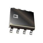
| 供应商器件封装 | 8-SOIC |
| 共模抑制比—最小值 | 54 dB |
| 包装 | 管件 |
| 压摆率 | 800 V/µs |
| 商标 | Analog Devices |
| 增益带宽积 | - |
| 安装类型 | 表面贴装 |
| 安装风格 | SMD/SMT |
| 封装 | Tube |
| 封装/外壳 | 8-SOIC(0.154",3.90mm 宽) |
| 封装/箱体 | SOIC-8 |
| 工作温度 | -40°C ~ 85°C |
| 工作电源电压 | 9 V to 12 V |
| 工厂包装数量 | 98 |
| 带宽 | 230 MHz |
| 拓扑结构 | Current Feedback |
| 放大器类型 | Current Feedback Amplifier |
| 最大工作温度 | + 85 C |
| 最小工作温度 | - 40 C |
| 标准包装 | 98 |
| 电压-电源,单/双 (±) | 9 V ~ 12 V, ±4.5 V ~ 6 V |
| 电压-输入失调 | 5mV |
| 电压增益dB | 114 dB |
| 电流-电源 | 15.5mA |
| 电流-输入偏置 | 10µA |
| 电流-输出/通道 | 200mA |
| 电源电压-最大 | 12 V |
| 电源电压-最小 | 9 V |
| 电源电流 | 17 mA |
| 电路数 | 1 |
| 稳定时间 | 25 ns |
| 系列 | AD8010 |
| 视频文件 | http://www.digikey.cn/classic/video.aspx?PlayerID=1364138032001&width=640&height=505&videoID=2245193153001http://www.digikey.cn/classic/video.aspx?PlayerID=1364138032001&width=640&height=505&videoID=2245193159001 |
| 转换速度 | 800 V/us |
| 输入补偿电压 | 5 mV |
| 输出电流 | 200 mA |
| 输出类型 | - |
| 通道数量 | 1 Channel |


- 商务部:美国ITC正式对集成电路等产品启动337调查
- 曝三星4nm工艺存在良率问题 高通将骁龙8 Gen1或转产台积电
- 太阳诱电将投资9.5亿元在常州建新厂生产MLCC 预计2023年完工
- 英特尔发布欧洲新工厂建设计划 深化IDM 2.0 战略
- 台积电先进制程称霸业界 有大客户加持明年业绩稳了
- 达到5530亿美元!SIA预计今年全球半导体销售额将创下新高
- 英特尔拟将自动驾驶子公司Mobileye上市 估值或超500亿美元
- 三星加码芯片和SET,合并消费电子和移动部门,撤换高东真等 CEO
- 三星电子宣布重大人事变动 还合并消费电子和移动部门
- 海关总署:前11个月进口集成电路产品价值2.52万亿元 增长14.8%


PDF Datasheet 数据手册内容提取
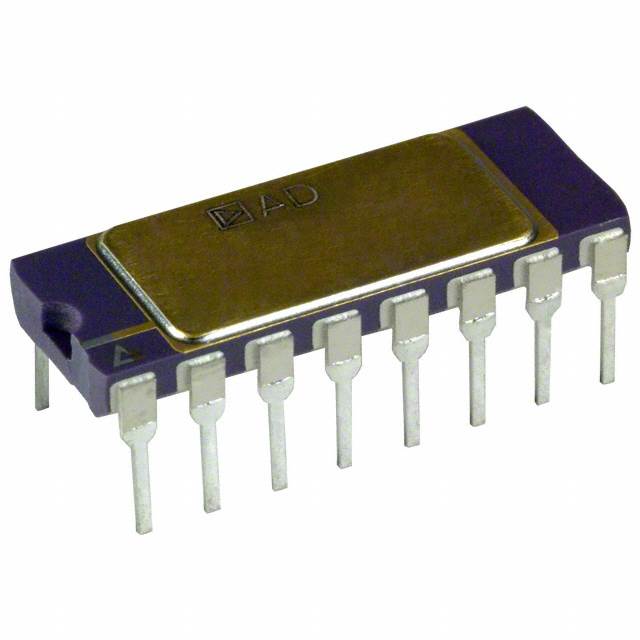
a 200 mA Output Current High-Speed Amplifier AD8010 FEATURES CONNECTION DIAGRAMS 200 mA of Output Current 9 (cid:1) Load 8-Lead DIP and SOIC SFDR –54 dBc @ 1 MHz Differential Gain Error 0.04%, f = 4.43 MHz AD8010 NC 1 8 NC Differential Phase Error 0.06(cid:2), f = 4.43 MHz –IN 2 7 +VS Maintains Video Specifications Driving Eight Parallel 75 (cid:1) Loads +IN 3 6 OUT 0.02% Differential Gain –VS 4 5 NC 0.03(cid:2) Differential Phase NC = NO CONNECT 0.1 dB Gain Flatness to 60 MHz THD –72 dBc @ 1 MHz, RL = 18.75 (cid:1) 16-Lead Wide Body SOIC IP3 42 dBm @ 5 MHz, R = 18.75 (cid:1) L 1 dB Gain Compression 21 dBm @ 5 MHz, R = 100 (cid:1) AD8010 230 MHz –3 dB Bandwidth, G = +1, R = 18.7L5 (cid:1) NC 1 16 NC 800 V/(cid:3)s Slew Rate, R = 18.75 (cid:1) L NC 2 15 NC 25 ns Settling Time to L0.1% –IN 3 14 +VS Available in 8-Lead DIP, 16-Lead Wide Body SOIC and NC 4 13 NC Thermally Enhanced 8-Lead SOIC +IN 5 12 OUT NC 6 11 NC APPLICATIONS –VS 7 10 NC Video Distribution Amplifier NC 8 9 NC VDSL, xDSL Line Driver Communications NC = NO CONNECT ATE Instrumentation PRODUCT DESCRIPTION 75(cid:1) VOUT1 The AD8010 is a low power, high current amplifier capable of delivering a minimum load drive of 175 mA. Signal performance RF VOUT2 such as 0.02% and 0.03° differential gain and phase error is RG +5V VOUT3 maintained while driving eight 75 Ω back terminated video lines. VOUT4 The current feedback amplifier features gain flatness to 60 MHz and –3 dB (G = +1) signal bandwidth of 230 MHz and only RS AD8010 VIN requires a typical of 15.5 mA supply current from ±5 V supplies. RT VOUT5 These features make the AD8010 an ideal component for Video –5V VOUT6 Distribution Amplifiers or as the drive amplifier within high data rate Digital Subscriber Line (VDSL and xDSL) systems. VOUT7 The AD8010 is an ideal component choice for any application VOUT8 that needs a driver that will maintain signal quality when driving 75(cid:1) low impedance loads. The AD8010 is offered in three package options: an 8-lead DIP, 16-lead wide body SOIC and a low thermal resistance 8-lead SOIC, and operates over the industrial temperature range of Figure 1.Video Distribution Amplifier –40°C to +85°C. REV.B Information furnished by Analog Devices is believed to be accurate and reliable. However, no responsibility is assumed by Analog Devices for its use, nor for any infringements of patents or other rights of third parties One Technology Way, P.O. Box 9106, Norwood, MA 02062-9106, U.S.A. which may result from its use. No license is granted by implication or Tel: 781/329-4700 World Wide Web Site: http://www.analog.com otherwise under any patent or patent rights of Analog Devices. Fax: 781/326-8703 © Analog Devices, Inc., 2000
AD8010–SPECIFICATIONS (@ 25(cid:2)C, V = (cid:4)5 V, G = +2, R = 18.75 (cid:1), R = 150 (cid:1), R = R = 604 (cid:1) (R-16), S L S+ F G R = R = 562 (cid:1) (N-8), R = R = 499 (cid:1) (R-8). T = –40(cid:2)C, T = +85(cid:2)C unless otherwise noted) F G F G MIN MAX Model Conditions Min Typ Max Unit DYNAMIC PERFORMANCE –3 dB Bandwidth G = +1, V = 0.2 V p-p 180 230 MHz OUT G = +2, V = 0.2 V p-p 130 190 MHz OUT 0.1 dB Bandwidth V = 0.2 V p-p 30 60 MHz OUT Large Signal Bandwidth V = 4 V p-p 90 MHz OUT Peaking V = 0.2 V p-p, < 5 MHz 0.02 dB OUT Slew V = 2 V p-p 800 V/µs OUT Rise and Fall Time V = 2 V p-p 2.0 ns OUT Settling Time 0.1%, V = 2 V p-p 25 ns OUT NOISE/HARMONIC PERFORMANCE Distortion V = 2 V p-p OUT 2nd Harmonic 1 MHz –73 dBc 5 MHz –58 dBc 10 MHz –53 dBc 10 MHz, R = 39 Ω –67 dBc L 20 MHz –44 dBc 3rd Harmonic 1 MHz –77 dBc 5 MHz –63 dBc 10 MHz –57 dBc 10 MHz, R = 39 Ω –63 dBc L 20 MHz –50 dBc IMD 5 MHz ∆f = 10 kHz –73 dBc IP3 5 MHz 42 dBm 1 dB Gain Compression 5 MHz 21 dBm Input Noise Voltage f = 10 kHz 2 nV√Hz Input Noise Current f = 10 kHz, +In 3 pA√Hz f = 20 kHz, –In 20 pA√Hz Differential Gain f = 4.43 MHz, R = 150 Ω 0.02 % L f = 4.43 MHz, R = 18.75 Ω 0.02 % L Differential Phase f = 4.43 MHz, R = 150 Ω 0.02 Degrees L f = 4.43 MHz, R =18.75 Ω 0.03 Degrees L DC PERFORMANCE Input Offset Voltage 5 12 mV T –T 15 mV MIN MAX Offset Drift 10 µV/°C Input Bias Current (–) 10 135 µA T –T 200 µA MIN MAX Input Bias Current (+) 6 12 µA T –T 20 µA MIN MAX INPUT CHARACTERISTICS Input Resistance +Input 125 kΩ –Input 12.5 Ω Input Capacitance 2.75 pF Common-Mode Rejection Ratio V = ±2.5 V 50 54 dB CM Input Common-Mode Voltage Range ±2.5 V Open Loop Transresistance V = ±2.5 V 300 500 kΩ OUT T –T 250 kΩ MIN MAX OUTPUT CHARACTERISTICS Output Voltage Swing R = 18.75 Ω ±2.1 ±2.5 V L R = 150 Ω ±2.7 ±3.0 V L Output Current R = 9 Ω 175 200 mA L Short-Circuit Current 240 mA Capacitive Load Drive 40 pF POWER SUPPLY Operating Range ±4.5 ±6.0 V Quiescent Current 15.5 17 mA T to T 20 mA MIN MAX Power Supply Rejection Ratio +V = +4 V to +6 V, –V = +5 V 60 66 dB S S +V = +5 V, –V = –4 V to –6 V 50 56 dB S S Specifications subject to change without notice. –2– REV. B
AD8010 ABSOLUTE MAXIMUM RATINGS1 MAXIMUM POWER DISSIPATION SupplyVoltage . . . . . . . . . . . . . . . . . . . . . . . . . . . . . . . 12.6V The maximum power that can be safely dissipated by the InternalPowerDissipation2 AD8010 is limited by the associated rise in junction temperature. PlasticPackage (N) . . . . . . Observe Power Derating Curves The maximum safe junction temperature for plastic encapsu- SmallOutlinePackage (R) . Observe Power Derating Curves lated devices is determined by the glass transition temperature Wide Body SOIC (R-16) . . . Observe Power Derating Curves of the plastic, approximately +150°C. Temporarily exceeding Input Voltage (Common-Mode) . . . . . . . . . . . . . . . . . . . ±V this limit may cause a shift in parametric performance due to a S DifferentialInputVoltage . . . . . . . . . . . . . . . . . . . . . . ±1.2V change in the stresses exerted on the die by the package. Exceed- Output Short Circuit Duration ing a junction temperature of +175°C for an extended period . . . . . . . . . . . . . . . . . . . . . . Observe Power Derating Curves can result in device failure. Storage Temperature Range N, R . . . . . . . . –65°C to +125°C While the AD8010 is internally short circuit protected, this Operating Temperature Range (A Grade) . . –40°C to +85°C may not be sufficient to guarantee that the maximum junction Lead Temperature Range (Soldering10sec) . . . . . . . . 300°C temperature (+150°C) is not exceeded under all conditions. To NOTES ensure proper operation, it is necessary to observe the maximum 1Stresses above those listed under Absolute Maximum Ratings may cause perma- power derating curves. nent damage to the device. This is a stress rating only; functional operation of the device at these or any other conditions above those indicated in the operational section of this specification is not implied. Exposure to absolute maximum rating conditions for extended periods may affect device reliability. 2Specification is for device in free air: 8-Lead Plastic Package: θJA = 90°C/W 8-Lead SOIC Package: θJA = 122°C/W 16-Lead SOIC Package: θJA = 73°C/W 3.0 TJ = 150(cid:2)C s Watt2.5 – 8-LEAD MINI-DIP PACKAGE N O TI2.0 PA 16-LEAD SOIC SI PACKAGE (WIDEBODY) S DI1.5 R E W O P1.0 8-LEAD SOIC PACKAGE M U M XI0.5 A M 0 –50 –40–30 –20 –10 0 10 20 30 40 50 60 70 80 90 AMBIENT TEMPERATURE – (cid:2)C Figure 2.Plot of Maximum Power Dissipation vs. Temperature ORDERING GUIDE Model Temperature Range Package Description Package Options AD8010AN –40°C to +85°C 8-Lead Plastic DIP N-8 AD8010AR –40°C to +85°C 8-Lead Plastic SOIC SO-8 AD8010AR-16 –40°C to +85°C 16-Lead Wide Body SOIC R-16 AD8010AR-REEL REEL SOIC 13" REEL AD8010AR-REEL7 REEL SOIC 7" REEL AD8010AR-16-REEL REEL SOIC 13" REEL AD8010AR-16-REEL7 REEL SOIC 7" REEL CAUTION ESD (electrostatic discharge) sensitive device. Electrostatic charges as high as 4000V readily WARNING! accumulate on the human body and test equipment and can discharge without detection. Although the AD8010 features proprietary ESD protection circuitry, permanent damage may occur on devices subjected to high-energy electrostatic discharges. Therefore, proper ESD ESD SENSITIVE DEVICE precautions are recommended to avoid performance degradation or loss of functionality. REV. B –3–
AD8010–Typical Performance Characteristics 60 0.05 0.10 SAMPLE SIZE = 300 dG G = +2 50 f = 4.43MHz (PAL) RL = 18.75(cid:1) 0.04 0.08 es GE OF UNITS3400 dG d(cid:6) d(cid:6)DDIIFFFFEERREENNTTIIAALL GPHAAINS dEG d (cid:6)IN I N% Degrees AL GAIN – % 0.03 DIFFERENTIAL GAIN 0.06 HASE – Degre PERCENTA20 dG d(cid:6) DIFFERENTI 0.02 DIFFERENTIAL PHASE 0.04 ERENTIAL P d(cid:6) 0.01 0.02 FF 10 DI d(cid:6) d(cid:6) dG d(cid:6) d(cid:6) d(cid:6) d(cid:6) d(cid:6) 0 0 0 0 0.010.020.030.040.050.060.070.080.090.100.110.120.13 1 2 4 6 8 10 12 14 16 dG (%)/d(cid:6) – Degrees NUMBER OF VIDEO LOADS Figure 3.Distribution of Differential Gain (dG) and Figure 6.Differential Gain and Phase vs. Number of Video Differential Phase (dφ); R = 18.75 Ω Loads Over Temperature (–40°C to +85°C); f = 4.43 MHz L –45 45 –50 G = +2 VO = 2V p-p 40 c –55 RL AS SHOWN B N – d –60 2ND dBm 35 RTIO –65 RL = 18.75(cid:1) 3RD NT – 30 C DISTO ––7705 EPT POI 25 GRL = = + 128.75(cid:1) MONI –80 3RD TERC 20 HAR –85 RL = 100(cid:1) 2ND IN 15 –90 10 –95 5 1 2 3 4 5 6 7 8 910 20 1 10 100 FREQUENCY – MHz FREQUENCY – MHz Figure 4.Harmonic Distortion vs. Frequency; G = +2 Figure 7.Two-Tone, 3rd Order IMD Intercept vs. Frequency; G = +2, R = 18.75 Ω L 6.5 4 6.20 GRL = = + 128.75(cid:1) +85(cid:2)C 6.4 GVO = = + 02.2V p-p 2 6.15 VO = 0.2V p-p 6.3 NUMBER OF VIDEO +25(cid:2)C LOADS AS SHOWN 6 GAIN FLATNESS – dB 6655....61099.05500 –40(cid:2)C GAIN FLATNESS – dB66655.....21098 1 8 10 5.85 5.7 12 5.80 5.6 14 5.5 0.1 1 10 100 500 1 10 100 1000 FREQUENCY – MHz FREQUENCY – MHz Figure 5.Gain Flatness vs. Frequency Over Temperature Figure 8.Gain Flatness vs. Frequency vs. Number of (–40°C to +85°C) Video Loads –4– REV. B
AD8010 5 0 POUT 4dBm 4dBm ORTION – dBm –––12555 GRf(cid:7)OLf = === + 5112M08k.H7Hz5z(cid:1) m –––132000 RG GAINP(RFM FU=E LA6LS.6 USR5CE0A =(cid:1)L 1E0)dBm N DIST –35 – dBRE –40 15500(cid:1)(cid:1) 50(cid:1) ATIO –45 EASU–50 500kHz TONE SPACING FROM DUL –55 PM–60 54 0M0IkSHSzI NTGO T5O.5NMEHSz WITH O RM –65 –69dBm –69dBm –70 E T IN –75 –80 –85 –90 4.965 4.985 5.0 5.015 5.035 0 1 2 3 4 5 6 7 8 9 10 FREQUENCY – MHz FREQUENCY – MHz Figure 9.Intermodulation Distortion Figure 12. Multitone Distortion; R = 100 Ω L –35 –55 FREQUENCY = 5MHz G = +2 – dBc –45 GRL = = + A2S SHOWN (SEE SCHEMATIC) Bc –60 fV =O 5=M 2HVz p-p ON –55 – d –65 TI N DISTOR –65 RL = 18.75(cid:1) TORTIO –70 ONIC –75 C DIS –75 RM RF ONI HA –85 RL = 100(cid:1) RG RM –80 2ND TOTAL –95 RL1 = FOR RL = 100(cid:1)PIN 15500(cid:1)(cid:1) RL1 50(cid:1)P5O0U(cid:1)T HA –85 3RD –105 RL1 = 23.1 FOR RL = 18.75(cid:1) –90 –10 –8 –6 –4 –2 0 2 4 6 8 10 12 15 100 200 300 400 500 POUT – dBm LOAD – (cid:1) Figure 10.Total Harmonic Distortion vs. P ; G = +2 Figure 13.Harmonic Distortion vs. Load OUT 2 G = +1 1 8.0 GVO = = + 20.2V p-p G = +2 7.0 NUMBER OF VIDEO LOADS AS SHOWN 4 0 1 B 6.0 – d –1 AIN –2 dB 5.0 D G G = +3 N – 4.0 LIZE –3 GAI 3.0 12 A M –4 GAIN AS SHOWN 8 OR VO = 0.2V p-p 2.0 N –5 RL = 18.75(cid:1) 1.0 –6 0.0 –7 0.1 1 10 100 1000 1 10 100 1000 FREQUENCY – MHz FREQUENCY – MHz Figure 11.Small Signal Closed-Loop Frequency Figure 14.Closed-Loop Frequency Response vs. Response; R = 18.75 Ω Number of Video Loads L REV. B –5–
AD8010 –10 0 –10 –20 –20 –30 –30 dB –40 dB–40 R – R – –50 R R S –50 M P C–60 –PSRR –60 –70 +PSRR –80 –70 –90 –80 –100 0.03 0.1 1 10 100 500 0.1 1 10 100 500 FREQUENCY – MHz FREQUENCY – MHz Figure 15.PSRR vs. Frequency Figure 18.CMRR vs. Frequency 1000 (cid:1) 310 E – G = +2 316 0 C 100 N A (cid:1) D-LOOP OUTPUT RESIST 03.133.01111 TRANSRESISTANCE – k 3311.011.0066 TRANSRESISTANCE PHASE 1194380550PHASE – Degrees E 0.1 S O 1 225 CL 0.031 0.316 0.1 1 10 100 500 10k 100k 1M 10M 100M 1G FREQUENCY – MHz FREQUENCY – Hz Figure 16.Closed-Loop Output Resistance vs. Frequency Figure 19.Transresistance and Phase vs. Frequency; R = 18.75 Ω L 2 3.0 1 G = +1 2.0 G = +2 1.0 0 B B d d 0.0 N – –1 GAIN AS SHOWN G = +2 N – ED GAI –2 VROL == 128V. 7p5-(cid:1)p ED GAI ––12..00 GAIN AS SHOWN G = +10 ALIZ –3 G = +10 ALIZ –3.0 VROL == 148V. 7p5-(cid:1)p M M R –4 R O O –4.0 N N –5 –5.0 –6 –6.0 –7 –7.0 0.1 1 10 100 1000 0.1 0 10 100 1000 FREQUENCY – MHz FREQUENCY – MHz Figure 17.Large Signal Frequency Response; V = 2 V p-p Figure 20.Large Signal Frequency Response; V = 4 V p-p O O –6– REV. B
AD8010 5 0.2 G = +1 4 G = +1 RL = 18.75(cid:1) RL = 18.75(cid:1) 0.15 VO = 0.2V p-p 3 VO = 4V p-p 0.1 2 0.05 1 S S LT 0 LT 0 O O V–0.05 V –1 –0.1 –2 –0.15 –3 –0.2 –4 50mV 20ns 1V 20ns –5 Figure 21.Small-Signal Pulse Response; G = +1 Figure 24.Large-Signal Pulse Response; G = +1 0.2 GRL = = + 128, .–715(cid:1) 4 GRL = = + 128, .–715(cid:1) 0.15 VO = 0.2V p-p 3 VO = 4V p-p 0.1 2 0.05 1 S S OLT 0 OLT 0 V–0.05 V–1 –0.1 –2 –0.15 –3 –0.2 –4 50mV 20ns 1V 20ns Figure 22.Small-Signal Pulse Response; G = +2, –1 Figure 25.Large-Signal Pulse Response; G = +2, –1 100 1000 Hz Hz GE NOISE – nV/ 10 NT NOISE – pA/ 100 INVERTING CURRENT A E T R INPUT VOL INPUT CUR 10 NONINVERTING CURRENT 1 1 10 100 1k 10k 100k 1M 10M 10 100 1k 10k 100k 1M 10M FREQUENCY – Hz FREQUENCY – Hz Figure 23.Input Voltage Noise vs. Frequency Figure 26.Input Current Noise vs. Frequency REV. B –7–
AD8010 Driving Capacitance Loads G = +6 RF = 604(cid:1) The AD8010 was designed primarily to drive nonreactive loads. RL = 18.75(cid:1) If driving loads with a capacitive component is desired, best frequency response is obtained by the addition of a small series INPUT resistance as shown in Figure 28. The inset figure shows the OUTPUT OLTS0 othpatti mthuem fr veaqluueen fcoyr rResSpERoInESs ev so.f ctahpea cciirtcivueit l owahde.n I td irsi vwinogr tlha rngoeting V capacitive loads will be dominated by the passive roll-off of R and C . SERIES L INPUT (500mV/DIV) LAYOUT CONSIDERATIONS OUTPUT (1V/DIV) 100ns The specified high speed performance of the AD8010 requires careful attention to board layout and component selection. Figure 27.Overdrive Recovery; G = +6 Proper R design techniques and low-pass parasitic component F selection are necessary. OVERDRIVE RECOVERY Overdrive of an amplifier occurs when the output and/or input The PCB should have a ground plane covering all unused portions range are exceeded. The amplifier must recover from this over- of the component side of the board to provide low impedance drive condition. As shown in Figure 27, the AD8010 recovers path. The ground plane should be removed from the area near the input pins to reduce the parasitic capacitance. within 35 ns from negative overdrive and within 75 ns from positive overdrive. +VS –VS THEORY OF OPERATION The AD8010 is a current feedback amplifier optimized for high current output while maintaining excellent performance with FB respect to flatness, distortion and differential gain/phase. As a C1 video distribution amplifier, the AD8010 will drive up to 12 + parallel video loads (12.5 Ω) from a single output with 0.04% 150(cid:1) differential gain and 0.04° differential phase errors. This means VIN RBT ZO that, unlike designs with one driver per output, any output is a RT AD8010 true reflection of the signal on all other outputs. C2 RL The high output current capability of the AD8010 also make it RF + useful in xDSL applications. The AD8010 can drive a 12.5Ω single-ended or 25 Ω differential load with low harmonic dis- tortion. This makes it useful in designs that utilize a step-up transformer to drive a twisted-pair transmission line. RG To achieve these levels of performance special precautions with respect to supply bypassing are recommended (Figure 29). This Figure 29.Standard Noninverting Closed-Loop Configura- configuration minimizes the contribution from high frequency tion with Recommended Bypassing Technique supply rejection to differential gain and phase errors as well as The standard noninverting closed-loop configuration with the reducing distortion due to harmonic energy in the power supplies. recommended power supply bypassing technique is shown in Figure 29. Ferrite beads (Amidon Associates, Torrance CA, 200 Part Number 43101) are used to suppress high frequency power GAIN AS SHOWN 100 VO = 0.2V p-p supply energy on the DUT supply lines at the DUT. C1 and C2 w/(cid:2) 30% OVERSHOOT each represent the parallel combination of a 47 µF (16 V) tanta- G = +5 F lum electrolytic capacitor, a 10 µF (10 V) tantalum electrolytic AD – p RG RF capacitor and a 0.1 µF ceramic chip capacitor. Connect C1 CITIVE LO 10 VIN 15500(cid:1)(cid:1) RCSL VOUT ftTrooh smei gf nteheaedl bg+arVocuSk nprdeins.i stoto trh seh –oVulSd p bine. lCocoantende cctl oCs2e tforo tmhe t hinev –eVrtSin pgin A P A input pin in order to keep the parasitic capacitance at this node C to a minimum. Parasitic capacitances of less than 1 pF at the G = +2 inverting input can significantly affect high speed performance. G = +1 Stripline design techniques should be used for long traces 1 (greater than about 3 cm). These should be designed with a 0 5 10 15 20 RS – (cid:1) characteristic impedance (ZO) of 50 Ω or 75 Ω and be properly terminated at each end. Figure 28.Capacitive Load Drive vs. Series Resistor for Various Gains –8– REV. B
AD8010 APPLICATIONS The bypassing scheme that is used for the AD8010 requires Video Distribution Amplifier special attention. It was found that the conventional technique The AD8010 is optimized for the specific function of providing of bypassing each power pin individually to ground can have an excellent video performance when driving multiple video loads adverse effect on the differential phase error of the circuit. The in parallel. Significant power is saved and heat sinking is greatly cause of this is attributed to the fact that there is an internal simplified because of the ability of the AD8010 to obtain this compensation capacitor in the AD8010 that is referenced to the performance when running on a ±5 V supply. However, due to negative supply. the high currents that flow when driving many parallel video The recommended technique is to connect parallel bypass loads, special layout and bypassing techniques are required to capacitors from the positive supply to the negative supply and assure optimal performance. then to bypass the negative supply to ground. For high fre- When designing a video distribution amplifier with the AD8010, it quency bypassing, 0.1 µF ceramic capacitors are recommended. is very important to keep in mind where the high (ac) currents These should be placed within a few millimeters of the power will flow. These paths include the power supply pins of the chip pins and should preferably be chip type capacitors. along with the bypass capacitors and the return path for these The high currents that can potentially flow through the power capacitors, the output circuits and the return path of the output supply pins require large bypassing capacitors. These should be current from the loads. low inductance tantalum types and at least 47 µF. The ground In general, any loops that are formed by any of the above paths side of the capacitor that bypasses the negative supply should be should be made as small as possible. Large loops are both gen- brought to a single point ground that is the common for the erators and receivers of magnetic fields and can cause undesired returns of the outputs. coupling of signals that lowers the performance of the amplifier. Figure 30 shows a circuit for making an N-channel video distri- Effects that have not been seen before in other op amp circuits bution amplifier. As a practical matter, the AD8010 can readily might arise because of the high currents. Most op amp circuits drive eight standard 150 Ω video loads. When driving up to 12 output, at most, tens of milliamps and do not require extremely video loads, there is minimal degradation in video performance. tight video specifications, while a video distribution amplifier Another important consideration when driving multiple cables can output hundreds of milliamps and require extremely low is the high frequency isolation between the outputs of the differential gain and phase errors. cables. Due to its low output impedance, the AD8010 achieves better than 46 dB of output-to-output isolation at 5 MHz driv- ing back terminated 75 Ω cables. +5V FB 499(cid:1) 499(cid:1) 75(cid:1) AD8010 VIN 150(cid:1) C1 75(cid:1) RL1 75(cid:1) 75(cid:1) C2 75(cid:1) RL2 FB –5V 75(cid:1) 75(cid:1) RLN Figure 30.An N-Channel Video Distribution Amplifier Using An AD8010. NOTE: Please see Figure 29 for Recommended Bypassing Technique. REV. B –9–
AD8010 Differential Line Driver In the circuit in Figure 31 the A device is configured as a gain- Twisted pair transmission lines are more often being used for of-two follower, while the B device is a gain-of-two inverter. high frequency analog and digital signals. Over long distances, These will produce a differential output signal whose maximum however, the attenuation characteristics of these lines can value is twice the peak-to-peak value of the maximum output degrade the performance of the transmission system. To com- of one device. For this circuit a 12 V peak-to-peak output can pensate for this, larger signals are transmitted, which after the be obtained. attenuation, will still have useful signal strength. The op amps drive a 1:2 step-up transformer that drives a The high output current of two AD8010s can be used along 100 Ω transmission line. Since the impedance reflected back to with a transformer to create a high power differential line driver. the primary varies as the square of the turns ratio, it will appear The differential configuration effectively doubles the output as 25 Ω at the primary. This source terminating resistor is split swing, while the step-up transformer further increases the out- as a 12.4 Ω resistor at the output of each device. put voltage. The circuit shown is capable of delivering 12 V p-p to the line and operates with a –3 dB bandwidth of 40 MHz. The peak current output of either op amp is 100 mA. 499(cid:1) 499(cid:1) 12.4(cid:1) +6 AD8010 150(cid:1) VIN 402(cid:1) 806(cid:1) 100(cid:1) 12.4(cid:1) AD8010 1:2 –6 150(cid:1) Figure 31.High Output Differential Line Driver Using Two AD8010s. NOTE: Please see Figure 29 for Recommended Bypassing Technique. –10– REV. B
AD8010 Closed-Loop Gain and Bandwidth Table I. –3 dB Bandwidth and Slew Rate vs. Closed-Loop The AD8010 is a current feedback amplifier optimized for use Gain and Resistor Values in high performance video and data acquisition applications. Since it uses a current feedback architecture, its closed-loop Package: N-8 –3 dB bandwidth is dependent on the magnitude of the feedback Closed-Loop –3 dB BW Slew Rate resistor. The desired closed-loop bandwidth and gain are obtained Gain R ((cid:1)) R ((cid:1)) (MHz) (V/(cid:3)s) F G by varying the feedback resistor (R ) to set the bandwidth, and F ∞ varying the gain resistor (R ) to set the desired gain. The char- +1 453 285 900 G acteristic curves and specifications for this data sheet reflect the +2 374 374 255 900 performance of the AD8010 using the values of R noted at the +5 348 86.6 200 800 F top of the specifications table. If a greater –3dB bandwidth +10 562 61.9 120 550 and/or slew rate is required (at the expense of video performance), Package: R-16 Table I provides the recommended resistor values. Figure 32 shows the test circuit and conditions used to produce Table I. Closed-Loop –3 dB BW Slew Rate Gain R ((cid:1)) R ((cid:1)) (MHz) (V/(cid:3)s) Effect of Feedback Resistor Tolerance on Gain Flatness F G ∞ Because of the relationship between the 3 dB bandwidth and the +1 412 245 900 feedback resistor, the fine scale gain flatness will, to some extent, +2 392 392 220 900 vary with feedback resistor tolerance. It is therefore recommended +5 392 97.6 160 800 that resistors with a 1% tolerance be used if it is desired to main- +10 604 66.5 95 550 tain flatness over a wide range of production lots. In addition, resistors of different construction have different associated para- Package: SO-8 sitic capacitance and inductance. Metal-film resistors were used Closed-Loop –3 dB BW Slew Rate for the bulk of the characterization for this data sheet. It is pos- Gain R ((cid:1)) R ((cid:1)) (MHz) (V/(cid:3)s) F G sible that values other than those indicated will be optimal for ∞ other resistor types. +1 392 345 950 +2 374 374 305 1000 Quality of Coaxial Cable +5 348 86.6 220 1000 Optimum flatness when driving a coax cable is possible only +10 499 54.9 135 650 when the driven cable is terminated at each end with a resistor matching its characteristic impedance. If the coax was ideal, 1. VO = 0.2 V p-p for –3 dB Bandwidth. 2. V = 2 V p-p for Slew Rate. then the resulting flatness would not be affected by the length of O 3. Bypassing per Figure 29. the cable. While outstanding results can be achieved using inex- pensive cables, it should be noted that some variation in flatness 150(cid:1) due to varying cable lengths may be experienced. VIN 50(cid:1) VOUT RF 18.75(cid:1) RG Figure 32.Test Circuit for Table I REV. B –11–
AD8010 OUTLINE DIMENSIONS Dimensions shown in inches and (mm). 8-Lead Plastic Mini-DIP (N-8) 0.430 (10.92) 0.348 (8.84) B) v. 8 5 0.280 (7.11) 0 (re 0.240 (6.10) 0 1 4 0.325 (8.25) 2/ 1 PIN 1 0.060 (1.52) 0.300 (7.62) –0– 0.015 (0.38) 0.195 (4.95) 7a 0.210 (5.33) 4 MAX 0.130 0.115 (2.93) 10 0.160 (4.06) (3.30) C0 0.115 (2.93) MIN 0.015 (0.381) 00..002124 ((00..535586))(02.1.5040)00..007405 ((11..7175)) SPELAANTIENG 0.008 (0.204) BSC 8-Lead SOIC (SO-8) 0.1968 (5.00) 0.1890 (4.80) 8 5 0.1574 (4.00) 0.2440 (6.20) 0.1497 (3.80) 1 4 0.2284 (5.80) PIN 1 0.0688 (1.75) 0.0196 (0.50) 0.0098 (0.25) 0.0532 (1.35) 0.0099 (0.25)(cid:8) 45(cid:2) 0.0040 (0.10) 8(cid:2) SEPALTAINNGE 0(B.10.S52C070) 00..00119328 ((00..4395)) 00..00009785 ((00..2159)) 0(cid:2) 00..00510600 ((10..2471)) 16-Lead Wide Body SOIC (R-16) 0.4133 (10.50) 0.3977 (10.00) 16 9 1 8 0.2992 (7.60)0.2914 (7.40)0.4193 (10.65)0.3937 (10.00) A. 0.0118 (0.30) PIN 1 00..10094236 ((22..6355)) 00..00209918 ((00..7245))(cid:8) 45(cid:2) U.S. 0.0040 (0.10) N D I 0(B.10.S25C70)0 00..00119328 ((00..4395)) SPELAANTIENG 00..00102951 ((00..3223))80(cid:2)(cid:2) 00..00510507 ((10..2470)) PRINTE –12– REV. B
Mouser Electronics Authorized Distributor Click to View Pricing, Inventory, Delivery & Lifecycle Information: A nalog Devices Inc.: AD8010ANZ AD8010ARZ AD8010ARZ-16