ICGOO在线商城 > 集成电路(IC) > 线性 - 放大器 - 仪表,运算放大器,缓冲器放大器 > MAX4450EUK+T

 Datasheet下载
- 型号: MAX4450EUK+T
- 制造商: Maxim
- 库位|库存: xxxx|xxxx
- 要求:
| 数量阶梯 | 香港交货 | 国内含税 |
| +xxxx | $xxxx | ¥xxxx |
查看当月历史价格
查看今年历史价格
MAX4450EUK+T产品简介:
ICGOO电子元器件商城为您提供MAX4450EUK+T由Maxim设计生产,在icgoo商城现货销售,并且可以通过原厂、代理商等渠道进行代购。 MAX4450EUK+T价格参考¥9.47-¥9.47。MaximMAX4450EUK+T封装/规格:线性 - 放大器 - 仪表,运算放大器,缓冲器放大器, 电压反馈 放大器 1 电路 满摆幅 SOT-23-5。您可以下载MAX4450EUK+T参考资料、Datasheet数据手册功能说明书,资料中有MAX4450EUK+T 详细功能的应用电路图电压和使用方法及教程。
MAX4450EUK+T 是 Maxim Integrated 公司推出的一款低功耗、高精度运算放大器,属于线性 - 放大器 - 仪表、运算放大器、缓冲器放大器类别。该型号具有以下特点和应用场景:

 特点:
1. 低功耗:MAX4450 的静态电流非常低(典型值为 200μA/通道),适合电池供电或对功耗要求严格的系统。
2. 高精度:输入失调电压低至 50μV(最大值),适用于高精度信号调理电路。
3. 宽带宽:单位增益带宽为 10MHz,能够处理高频信号。
4. 轨到轨输出:支持接近电源电压范围的输出摆幅,提高了动态范围。
5. 工作电压范围广:支持单电源供电(2.7V 至 5.5V),适应多种电源环境。

 应用场景:
1. 医疗设备:
   - 用于心率监测仪、血压计等便携式医疗设备中,对微弱生物电信号进行放大和处理。
   - 在血糖仪中,作为信号调理放大器,确保测量结果的高精度。

2. 工业自动化:
   - 传感器信号放大:例如温度、压力或位移传感器的信号调理,提供高精度的输出。
   - 数据采集系统:用于模数转换器(ADC)前端,提高信号质量。

3. 消费电子:
   - 音频信号处理:在低功耗音频设备中,如耳机放大器或语音识别模块,提供清晰的音频信号。
   - 智能家居设备:如环境监测传感器(温湿度、光照等)的信号放大。

4. 通信系统:
   - 用于低功耗无线模块中的信号调理,确保信号传输的稳定性和准确性。
   - 在射频前端电路中,作为缓冲放大器,减少信号失真。

5. 汽车电子:
   - 车载传感器信号处理:如胎压监测系统(TPMS)中,对压力和温度信号进行放大。
   - 信息娱乐系统:用于音频信号的低功耗放大。

6. 测试与测量:
   - 在便携式测试仪器中,如示波器或万用表,提供高精度的信号放大功能。
   - 数据记录仪:用于长时间记录微弱信号的变化。

总之,MAX4450EUK+T 凭借其低功耗、高精度和宽电压范围的特点,广泛应用于需要高效信号处理的各种领域,特别是在便携式和电池供电设备中表现出色。
| 参数 | 数值 |
| -3db带宽 | 210MHz |
| 产品目录 | 集成电路 (IC)半导体 |
| 描述 | IC OPAMP VFB 210MHZ RRO SOT23-5高速运算放大器 210MHz Single-Supply w/Rail-Rail Output |
| 产品分类 | Linear - Amplifiers - Instrumentation, OP Amps, Buffer Amps集成电路 - IC |
| 品牌 | Maxim Integrated |
| 产品手册 | |
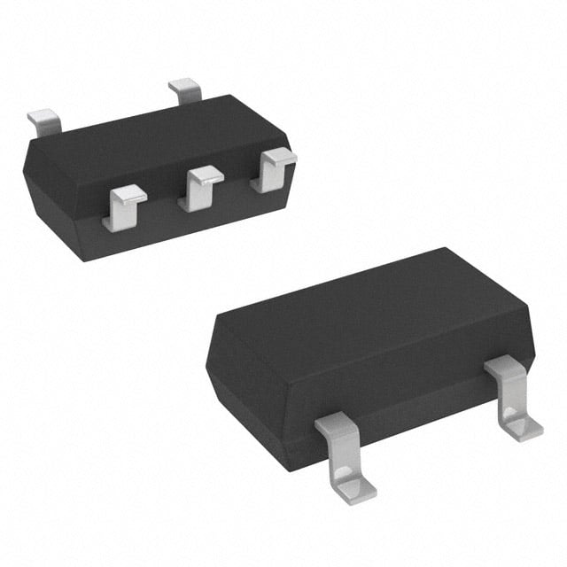
| 产品图片 |
|
| rohs | 符合RoHS无铅 / 符合限制有害物质指令(RoHS)规范要求 |
| 产品系列 | 放大器 IC,高速运算放大器,Maxim Integrated MAX4450EUK+T- |
| 数据手册 | |
| 产品型号 | MAX4450EUK+T |
| 产品 | Voltage Feedback Amplifier |
| 产品培训模块 | http://www.digikey.cn/PTM/IndividualPTM.page?site=cn&lang=zhs&ptm=25703http://www.digikey.cn/PTM/IndividualPTM.page?site=cn&lang=zhs&ptm=25705 |
| 产品目录页面 | |
| 产品种类 | 高速运算放大器 |
| 供应商器件封装 | SOT-23-5 |
| 共模抑制比—最小值 | 70 dB |
| 其它名称 | MAX4450EUK+TDKR |
| 包装 | Digi-Reel® |
| 压摆率 | 485 V/µs |
| 商标 | Maxim Integrated |
| 增益带宽积 | - |
| 安装类型 | 表面贴装 |
| 安装风格 | SMD/SMT |
| 封装 | Reel |
| 封装/外壳 | SC-74A,SOT-753 |
| 封装/箱体 | SOT-23-5 |
| 工作温度 | -40°C ~ 85°C |
| 工作电源电压 | 4.5 V to 11 V |
| 工厂包装数量 | 2500 |
| 带宽 | 210 MHz |
| 应用说明 | |
| 拓扑结构 | Voltage Feedback |
| 放大器类型 | 电压反馈 |
| 最大功率耗散 | 571 mW |
| 最大工作温度 | + 85 C |
| 最小工作温度 | - 40 C |
| 标准包装 | 1 |
| 电压-电源,单/双 (±) | 4.5 V ~ 11 V, ±2.25 V ~ 5.5 V |
| 电压-输入失调 | 4mV |
| 电压增益dB | 58 dB |
| 电流-电源 | 6.5mA |
| 电流-输入偏置 | 6.5µA |
| 电流-输出/通道 | 70mA |
| 电源电压-最大 | 11 V |
| 电源电压-最小 | 4.5 V |
| 电源电流 | 6.5 mA |
| 电路数 | 1 |
| 系列 | MAX4450 |
| 转换速度 | 485 V/us |
| 输入补偿电压 | 26 mV |
| 输出电流 | 50 mA |
| 输出类型 | 满摆幅 |
| 通道数量 | 1 Channel |
| 零件号别名 | MAX4450 |


PDF Datasheet 数据手册内容提取
19-1522; Rev 4; 11/09 Ultra-Small, Low-Cost, 210MHz, Single-Supply Op Amps with Rail-to-Rail Outputs General Description Features M The MAX4450 single and MAX4451 dual op amps are ♦ Ultra-Small SC705 and SOT23 Packages A unity-gain-stable devices that combine high-speed per- formance with rail-to-rail outputs. Both devices operate ♦ Low Cost X from a +4.5V to +11V single supply or from ±2.25V to ♦ High Speed 4 ±5.5V dual supplies. The common-mode input voltage 210MHz -3dB Bandwidth 4 range extends beyond the negative power-supply rail (ground in single-supply applications). 55MHz 0.1dB Gain Flatness 5 485V/µs Slew Rate The MAX4450/MAX4451 require only 6.5mA of quies- 0 cent supply current per op amp while achieving a ♦ Single +4.5V to +11V Operation / M 210MHz -3dB bandwidth and a 485V/µs slew rate. Both ♦ Rail-to-Rail Outputs devices are an excellent solution in low-power/low- A voltage systems that require wide bandwidth, such as ♦ Input Common-Mode Range Extends Beyond VEE video, communications, and instrumentation. ♦ Low Differential Gain/Phase: 0.02%/0.08° X The MAX4450 is available in the ultra-small 5-pin SC70 4 ♦ Low Distortion at 5MHz package, while the MAX4451 is available in space- 4 saving 8-pin SOT23 and SO packages. -65dBc SFDR 5 -63dB Total Harmonic Distortion 1 Applications Set-Top Boxes Ordering Information Surveillance Video Systems Battery-Powered Instruments PIN- TOP PART TEMP RANGE Video Line Driver PACKAGE MARK Analog-to-Digital Converter Interface MAX4450EXK-T -40°C to +85°C 5 SC70 AAA CCD Imaging Systems MAX4450EUK-T -40°C to +85°C 5 SOT23 ADKP Video Routing and Switching Systems MAX4451EKA-T -40°C to +85°C 8 SOT23 AAAA Digital Cameras MAX4451ESA -40°C to +85°C 8 SO — Typical Operating Circuit Pin Configurations TOP VIEW IN 75Ω OUT OUT 1 5 VCC Zo = 75Ω MAX4450 MAX4450 75Ω VEE 2 IN+ 3 4 IN- 500Ω 500Ω SC70/SOT23 Pin Configurations continued at end of data sheet. VIDEO LINE DRIVER ________________________________________________________________Maxim Integrated Products 1 For pricing, delivery, and ordering information,please contact Maxim/Dallas Direct!at 1-888-629-4642, or visit Maxim’s website at www.maxim-ic.com.
Ultra-Small, Low-Cost, 210MHz, Single-Supply Op Amps with Rail-to-Rail Outputs 1 ABSOLUTE MAXIMUM RATINGS 5 Supply Voltage (VCCto VEE)................................................+12V 8-Pin SOT23-8 (derate 5.26mW/°C above +70°C)......421mW 4 IN_-, IN_+, OUT_..............................(VEE- 0.3V) to (VCC+ 0.3V) 8-Pin SO (derate 5.9mW/°C above +70°C).................471mW 4 Output Short-Circuit Current to VCCor VEE......................150mA Operating Temperature Range...........................-40°C to +85°C Continuous Power Dissipation (TA= +70°C) Storage Temperature Range.............................-65°C to +150°C X 5-Pin SC70-5 (derate 2.5mW/°C above +70°C)..........200mW Lead Temperature (soldering, 10s).................................+300°C 5-Pin SOT23-5 (derate 7.1mW/°C above +70°C)........571mW A M Stresses beyond those listed under “Absolute Maximum Ratings” may cause permanent damage to the device. These are stress ratings only, and functional operation of the device at these or at any other conditions beyond those indicated in the operational sections of the specifications is not implied. Exposure to absolute maximum rating conditions for extended periods may affect device reliability. / 0 DC ELECTRICAL CHARACTERISTICS 5 ∞ 4 (VCC= +5V, VEE= 0V, RL= to VCC/2, VOUT= VCC/2, TA= TMINto TMAX, unless otherwise noted. Typical values are at TA= +25°C.) (Note 1) 4 PARAMETER SYMBOL CONDITIONS MIN TYP MAX UNITS X Input Common-Mode VEE- VCC A VCM Guaranteed by CMRR test V Voltage Range 0.20 2.25 M Input Offset Voltage (Note 2) VOS 4 26 mV Input Offset Voltage Matching 1.0 mV Input Offset Voltage TCVOS 8 µV/°C Temperature Coefficient Input Bias Current IB (Note 2) 6.5 20 µA Input Offset Current IOS (Note 2) 0.5 4 µA Differential mode (-1V ≤VIN≤+1V) 70 kΩ Input Resistance RIN Common mode (-0.2V ≤VCM≤+2.75V) 3 MΩ Common-Mode Rejection Ratio CMRR (VEE - 0.2V) ≤VCM ≤(VCC - 2.25V) 70 95 dB 0.25V ≤VOUT≤4.75V, RL= 2kΩ 50 60 Open-Loop Gain (Note 2) AVOL 0.5V ≤VOUT≤4.5V, RL= 150Ω 48 58 dB 1V ≤VOUT≤4V, RL= 50Ω 57 RL= 2kΩ VCC- VOH 0.05 0.20 VOL- VEE 0.05 0.15 Output Voltage Swing RL= 150Ω VCC- VOH 0.30 0.50 VOUT VOL- VEE 0.25 0.80 (Note 2) V VCC- VOH 0.5 0.80 RL= 75Ω VOL- VEE 0.5 1.75 Sourcing 45 70 Output Current IOUT RL= 50Ω mA Sinking 25 50 Output Short-Circuit Current ISC Sinking or sourcing ±120 mA Open-Loop Output Resistance ROUT 8 Ω Power-Supply Rejection Ratio VEE= 0V, VCM= 2V 46 62 PSRR VCC= 5V dB (Note 3) VEE= -5V, VCM= 0V 54 69 Operating Supply-Voltage VS VCCto VEE 4.5 11.0 V Range Quiescent Supply Current IS 6.5 9.0 mA (per amplifier) 2 _______________________________________________________________________________________
Ultra-Small, Low-Cost, 210MHz, Single-Supply Op Amps with Rail-to-Rail Outputs AC ELECTRICAL CHARACTERISTICS M (VCC= +5V, VEE= 0V, VCM= +2.5V, RF= 24Ω, RL= 100Ωto VCC/2, VOUT= VCC/2, AVCL= +1V/V, TA= +25°C, unless otherwise A noted.) X PARAMETER SYMBOL CONDITIONS MIN TYP MAX UNITS 4 Small-Signal -3dB Bandwidth BWSS VOUT= 100mVP-P 210 MHz 4 Large-Signal -3dB Bandwidth BWLS VOUT= 2VP-P 175 MHz 5 Bandwidth for 0.1dB Gain BW0.1dB VOUT= 100mVP-P 55 MHz 0 Flatness / Slew Rate SR VOUT= 2V step 485 V/µs M Settling Time to 0.1% tS VOUT= 2V step 16 ns A Rise/Fall Time tR, tF VOUT= 100mVP-P 4 ns X Spurious-Free Dynamic SFDR fC= 5MHz, VOUT= 2VP-P -65 dBc 4 Range 4 2nd harmonic -65 5 Harmonic Distortion HD fC= 5MHz, 3rd harmonic -58 dBc 1 VOUT= 2VP-P Total harmonic -63 distortion Two-Tone, Third-Order IP3 f1 = 4.7MHz, f2 = 4.8MHz, VOUT = 1VP-P 66 dBc Intermodulation Distortion Channel-to-Channel Isolation CHISO Specified at DC 102 dB Input 1dB Compression Point fC= 10MHz, AVCL= +2V/V 14 dBm Differential Phase Error DP NTSC, RL= 150Ω 0.08 degrees Differential Gain Error DG NTSC, RL= 150Ω 0.02 % Input Noise-Voltage Density en f = 10kHz 10 nV/√Hz Input Noise-Current Density in f = 10kHz 1.8 pA/√Hz Input Capacitance CIN 1 pF Output Impedance ZOUT f = 10MHz 1.5 Ω Note 1: All devices are 100% production tested at TA= +25°C. Specifications over temperature limits are guaranteed by design. Note 2: Tested with VCM= +2.5V. Note 3: PSR for single +5V supply tested with VEE= 0V, VCC= +4.5V to +5.5V; PSR for dual ±5V supply tested with VEE= -4.5V to -5.5V, VCC= +4.5V to +5.5V. _______________________________________________________________________________________ 3
Ultra-Small, Low-Cost, 210MHz, Single-Supply Op Amps with Rail-to-Rail Outputs 1 Typical Operating Characteristics 5 (VCC= +5V, VEE= 0V, VCM= +2.5V, AVCL= +1V/V, RF= 24Ω, RL= 100Ωto VCC/2, TA = +25°C, unless otherwise noted.) 4 4 X SMALL-SIGNAL GAIN vs. FREQUENCY LARGE-SIGNAL GAIN vs. FREQUENCY GAIN FLATNESS vs. FREQUENCY MA 423 VOUT = 100mVP-P MAX4450-01 423 VOUT = 2VP-P MAX4450-02 000...423 VOUT = 100mVP-P MAX4450-03 0/ 1 1 0.1 445 GAIN (dB) --210 GAIN (dB) --210 GAIN (dB) --00..210 -3 -3 -0.3 X -4 -4 -0.4 A -5 -5 -0.5 M -6 -6 -0.6 100k 1M 10M 100M 1G 100k 1M 10M 100M 1G 100k 1M 10M 100M 1G FREQUENCY (Hz) FREQUENCY (Hz) FREQUENCY (Hz) OUTPUT IMPEDANCE vs. FREQUENCY DISTORTION vs. FREQUENCY DISTORTION vs. FREQUENCY 100 MAX4450-04 --12000 VAOVCULT == +21VVP-/PV MAX4450-05 --12000 VAOVCULT == +22VVP-/PV MAX4450-06 10 Ω) Bc) -30 Bc) -30 IMPEDANCE ( 1 DISTORTION (d ---546000 2ND HARMONIC DISTORTION (d ---546000 2ND HARMONIC -70 -70 0.1 3RD HARMONIC -80 3RD HARMONIC -80 -90 -90 0.01 -100 -100 100k 1M 10M 100M 1G 100k 1M 10M 100M 100k 1M 10M 100M FREQUENCY (Hz) FREQUENCY (Hz) FREQUENCY (Hz) DISTORTION vs. FREQUENCY DISTORTION vs. RESISTIVE LOAD DISTORTION vs. VOLTAGE SWING --12000 VAOVCULT == +25VVP-/PV MAX4450-07 --21000 fVAOOV =CU LT5 =M= +2H1VzVP-/PV MAX4450-08 --21000 AfOV =C L5 =M +H1zV/V MAX4450-09 DISTORTION (dBc) -----5473600000 2ND3 HRADR HMAORNMICONIC DISTORTION (dBc) -----7654300000 2ND HARMONIC DISTORTION (dBc) -----7654300000 3RD HARMONIC -80 -80 -80 2ND HARMONIC 3RD HARMONIC -90 -90 -90 -100 -100 -100 100k 1M 10M 100M 0 200 400 600 800 1000 1200 0.5 1.0 1.5 2.0 FREQUENCY (Hz) RLOAD (Ω) VOLTAGE SWING (Vp-p) 4 _______________________________________________________________________________________
Ultra-Small, Low-Cost, 210MHz, Single-Supply Op Amps with Rail-to-Rail Outputs Typical Operating Characteristics (continued) M (VCC= +5V, VEE= 0, VCM= +2.5V, AVCL= +1V/V, RF= 24Ω, RL= 100Ωto VCC/2, TA = +25°C, unless otherwise noted.) A X COMMON-MODE REJECTION POWER-SUPPLY REJECTION 4 DIFFERENTIAL GAIN AND PHASE vs. FREQUENCY vs. FREQUENCY 4 DIFF GAIN (%) 00000.....0000002112500055 MAX4450-10 ---3210000 MAX4450-11 ---3210000 MAX4450-12 50/M -0.005 SE (degrees)-000000.0.....0010116804200 IRE 100 CMR (dB) -----8765400000 PSR (dB)-----8765400000 AX44 PHA 0.002 -90 -90 5 DIFF --00..0042 -100 -100 1 0 100 100k 1M 10M 100M 1G 100k 1M 10M 100M 1G IRE FREQUENCY (Hz) FREQUENCY (Hz) OUTPUT VOLTAGE SWING vs. RESISTIVE LOAD SMALL-SIGNAL PULSE RESPONSE SMALL-SIGNAL PULSE RESPONSE 11..46 MAX4450-13 INPUT MAX4450-14 INPUT MAX4450-15 V) 50mV/div 25mV/div G ( 1.2 N T VOLTAGE SWI 010...608 VCC - VOH VOLTAGE (V) VOLTAGE (V) U OUTP 0.4 VOL - VEE 5O0UmTVP/dUiTv 5O0UmTVP/dUiTv 0.2 RF = 24Ω RF = 500Ω AVCL = +1V/V AVCL = +2V/V 0 0 50 100 150 200 250 300 350 400 450 500 20ns/div 20ns/div RLOAD (Ω) SMALL-SIGNAL PULSE RESPONSE LARGE-SIGNAL PULSE RESPONSE LARGE-SIGNAL PULSE RESPONSE INPUT MAX4450-16 INPUT MAX4450-17 INPUT MAX4450-18 10mV/div 1V/div 500mV/div GE (V) GE (V) GE (V) OLTA OLTA OLTA V V V OUTPUT OUTPUT OUTPUT 50mV/div 1V/div 1V/div RAFV C=L 5=0 +05ΩV/V RAFV C=L 2 =4 Ω+1V/V RAFV C=L 5=0 +02ΩV/V 20ns/div 20ns/div 20ns/div _______________________________________________________________________________________ 5
Ultra-Small, Low-Cost, 210MHz, Single-Supply Op Amps with Rail-to-Rail Outputs 1 Typical Operating Characteristics (continued) 5 (VCC= +5V, VEE= 0, VCM= +2.5V, AVCL= +1V/V, RF= 24Ω, RL= 100Ωto VCC/2, TA = +25°C, unless otherwise noted.) 4 4 LARGE-SIGNAL PULSE RESPONSE VOLTAGE NOISE vs. FREQUENCY CURRENT NOISE vs. FREQUENCY AX INPUT MAX4450-19 100 MAX4450-20 100 MAX4450-21 450/M VOLTAGE (V)1INVP/dUiTv √VOLTAGE NOISE (nV/Hz) 10 √CURRENT NOISE (pA/Hz) 10 4 1V/div X RF = 500Ω AVCL = +2V/V RL = 100Ω RL = 100Ω A 1 1 20ns/div 1 10 100 1k 10k 100k 1M 10M 1 10 100 1k 10k 100k 1M 10M M FREQUENCY (Hz) FREQUENCY (Hz) ISOLATION RESISTANCE SMALL-SIGNAL BANDWIDTH vs. CAPACITIVE LOAD vs. LOAD RESISTANCE 1156 MAX4450-22 235000 MAX4450-23 14 Hz)200 M Ω) 13 SMALL SIGNAL H ( R (ISO 12 (VOUT = 100mVP-P) DWIDT150 N BA100 11 50 10 LARGE SIGNAL (VOUT = 2VP-P) 9 0 0 50 100 150 200 250 300 350 400 450 500 0 100 200 300 400 500 600 700 800 CLOAD (pF) RLOAD (Ω) MAX4451 OPEN-LOOP GAIN vs. RESISTIVE LOAD CROSSTALK vs. FREQUENCY 7800 MAX4450-24 246000 MAX4450-25 60 Bc) 0 AIN (d 50 K (dB) -20 OP G 40 STAL -40 O S EN-L 30 CRO -60 OP -80 20 -100 10 -120 0 -140 100 1k 10k 0.1M 1M 10M 100M 1G RLOAD (Ω) FREQUENCY (Hz) 6 _______________________________________________________________________________________
Ultra-Small, Low-Cost, 210MHz, Single-Supply Op Amps with Rail-to-Rail Outputs Pin Description Inverting and Noninverting Configurations M Select the gain-setting feedback (RF) and input (RG) resistor values to fit your application. Large resistor val- A PIN NAME FUNCTION ues increase voltage noise and interact with the amplifi- X MAX4450 MAX4451 er’s input and PC board capacitance. This can 4 1 — OUT Amplifier Output generate undesirable poles and zeros and decrease bandwidth or cause oscillations. For example, a nonin- 4 Negative Power Supply 2 4 VEE or Ground (in single- verting gain-of-two configuration (RF = RG) using 1kΩ 5 supply operation) resistors, combined with 1pF of amplifier input capaci- 0 tance and 1pF of PC board capacitance, causes a pole 3 — IN+ Noninverting Input at 159MHz. Since this pole is within the amplifier band- /M 4 — IN- Inverting Input width, it jeopardizes stability. Reducing the 1kΩ resis- A 5 8 VCC Positive Power Supply tors to 100Ω extends the pole frequency to 1.59GHz, but could limit output swing by adding 200Ω in parallel X — 1 OUTA Amplifier A Output with the amplifier’s load resistor. Table 1 lists suggest- 4 Amplifier A Inverting ed feedback and gain resistors, and bandwidths for — 2 INA- 4 Input several gain values in the configurations shown in 5 Figures 1a and 1b. Amplifier A Noninverting — 3 INA+ 1 Input Layout and Power-Supply Bypassing — 7 OUTB Amplifier B Output These amplifiers operate from a single +4.5V to +11V power supply or from dual ±2.25V to ±5.5V supplies. For Amplifier B Inverting — 6 INB- Input single-supply operation, bypass VCC to ground with a Amplifier B Noninverting — 5 INB+ Input RG RF Detailed Description The MAX4450/MAX4451 are single-supply, rail-to-rail, voltage-feedback amplifiers that employ current-feed- RTO VOUT MAX445 _ back techniques to achieve 485V/µs slew rates and 210MHz bandwidths. Excellent harmonic distortion and IN VOUT = [1+ (RF / RG)] VIN RO differential gain/phase performance make these ampli- RTIN fiers an ideal choice for a wide variety of video and RF signal-processing applications. The output voltage swings to within 55mV of each sup- ply rail. Local feedback around the output stage Figure 1a. Noninverting Gain Configuration ensures low open-loop output impedance to reduce gain sensitivity to load variations. The input stage per- mits common-mode voltages beyond the negative sup- ply and to within 2.25V of the positive supply rail. RG RF IN Applications Information Choosing Resistor Values RTIN RTO VOUT MAX445 _ Unity-Gain Configuration The MAX4450/MAX4451 are internally compensated for VOUT = -(RF / RG) VIN RO unity gain. When configured for unity gain, the devices RS require a 24Ω resistor (RF) in series with the feedback path. This resistor improves AC response by reducing the Q of the parallel LC circuit formed by the parasitic feedback capacitance and inductance. Figure 1b. Inverting Gain Configuration _______________________________________________________________________________________ 7
Ultra-Small, Low-Cost, 210MHz, Single-Supply Op Amps with Rail-to-Rail Outputs 1 Table 1. Recommended Component Values 5 GAIN (V/V) 4 COMPONENT 4 +1 -1 +2 -2 +5 -5 +10 -10 +25 -25 X RF(Ω) 24 500 500 500 500 500 500 500 500 1200 A RG(Ω) ∞ 500 500 250 124 100 56 50 20 50 M RS(Ω) — 0 — 0 — 0 — 0 — 0 / 0 RTIN(Ω) 49.9 56 49.9 62 49.9 100 49.9 ∞ 49.9 ∞ 5 RTO(Ω) 49.9 49.9 49.9 49.9 49.9 49.9 49.9 49.9 49.9 49.9 4 4 Small-Signal -3dB Bandwidth (MHz) 210 100 95 50 25 25 11 15 5 10 X Note: RL = RO + RTO; RTIN and RTO are calculated for 50Ω applications. For 75Ω systems, RTO = 75Ω; calculate RTIN from the A following equation: 75 R = Ω TIN M 75 1- R G 0.1µF capacitor as close to the pin as possible. If operat- and the rail-to-rail output substantially increase the ing with dual supplies, bypass each supply with a 0.1µF dynamic range. With a symmetric input in a single +5V capacitor. application, the input can swing 2.95VP-P and the out- Maxim recommends using microstrip and stripline tech- put can swing 4.9VP-Pwith minimal distortion. niques to obtain full bandwidth. To ensure that the PC Output Capacitive Loading and Stability board does not degrade the amplifier’s performance, The MAX4450/MAX4451 are optimized for AC perfor- design it for a frequency greater than 1GHz. Pay care- mance. They are not designed to drive highly reactive ful attention to inputs and outputs to avoid large para- loads, which decrease phase margin and may produce sitic capacitance. Whether or not you use a constant- excessive ringing and oscillation. Figure 2 shows a cir- impedance board, observe the following design guide- cuit that eliminates this problem. Figure 3 is a graph of lines: the optimal isolation resistor (RS) vs. capacitive load. • Don’t use wire-wrap boards; they are too inductive. Figure 4 shows how a capacitive load causes exces- sive peaking of the amplifier’s frequency response if • Don’t use IC sockets; they increase parasitic capaci- the capacitor is not isolated from the amplifier by a tance and inductance. resistor. A small isolation resistor (usually 20Ω to 30Ω) • Use surface-mount instead of through-hole compo- placed before the reactive load prevents ringing and nents for better high-frequency performance. oscillation. At higher capacitive loads, AC performance • Use a PC board with at least two layers; it should be is controlled by the interaction of the load capacitance as free from voids as possible. and the isolation resistor. Figure 5 shows the effect of a 27Ωisolation resistor on closed-loop response. • Keep signal lines as short and as straight as possi- ble. Do not make 90°turns; round all corners. Coaxial cable and other transmission lines are easily driven when properly terminated at both ends with their Rail-to-Rail Outputs, characteristic impedance. Driving back-terminated Ground-Sensing Input transmission lines essentially eliminates the line’s The input common-mode range extends from capacitance. (VEE - 200mV) to (VCC - 2.25V) with excellent common- mode rejection. Beyond this range, the amplifier output is a nonlinear function of the input, but does not under- go phase reversal or latchup. The output swings to within 55mV of either power- supply rail with a 2kΩ load. The input ground sensing 8 _______________________________________________________________________________________
Ultra-Small, Low-Cost, 210MHz, Single-Supply Op Amps with Rail-to-Rail Outputs M 30 A X Ω) 25 RG RF E, R (ISO 20 44 C N 5 A RISO SIST 15 0 MAX445 _ VOUT ON RE 10 /M VIN CL ATI L RTIN 50Ω ISO 5 A X 0 4 0 50 100 150 200 250 4 CAPACITIVE LOAD, CL (pF) 5 1 Figure 2. Driving a Capacitive Load Through an Isolation Resistor Figure 3. Capacitive Load vs. Isolation Resistance 6 3 RISO = 27Ω 5 CL = 15pF 2 CL = 47pF 4 1 3 0 N (dB) 21 CL = 10pF N (dB) --12 CL = 68pF AI AI G 0 G -3 CL = 120pF -1 CL = 5pF -4 -2 -5 -3 -6 -4 -7 100k 1M 10M 100M 1G 100k 1M 10M 100M 1G FREQUENCY (Hz) FREQUENCY (Hz) Figure 4. Small-Signal Gain vs. Frequency with Load Figure 5. Small-Signal Gain vs. Frequency with Load Capacitance and No Isolation Resistor Capacitance and 27ΩIsolation Resistor _______________________________________________________________________________________ 9
Ultra-Small, Low-Cost, 210MHz, Single-Supply Op Amps with Rail-to-Rail Outputs 1 Pin Configurations (continued) Chip Information 5 4 MAX4450 TRANSISTOR COUNT: 86 4 TOP VIEW MAX4451 TRANSISTOR COUNT: 170 X A M OUTA 1 8 VCC INA- 2 7 OUTB 0/ MAX4451 INA+ 3 6 INB- 5 4 VEE 4 5 INB+ 4 X SOT23/SO A M 10 ______________________________________________________________________________________
Ultra-Small, Low-Cost, 210MHz, Single-Supply Op Amps with Rail-to-Rail Outputs Package Information M For the latest package outline information and land patterns, go to www.maxim-ic.com/packages. Note that a “+”, “#”, or “-” in the A package code indicates RoHS status only. Package drawings may show a different suffix character, but the drawing pertains to the package regardless of RoHS status. X 4 PACKAGE TYPE PACKAGE CODE DOCUMENT NO. 4 5 SC70 X5-1 21-0076 5 5 SOT23 U5-2 21-0057 0 8 SOT23 K8-2 21-0078 / M 8 SO S8-5 21-0041 A S EP X L. 5 0, 4 7 SC 4 5 1 PACKAGE OUTLINE, 5L SC70 1 21-0076 E 1 ______________________________________________________________________________________ 11
Ultra-Small, Low-Cost, 210MHz, Single-Supply Op Amps with Rail-to-Rail Outputs 1 Package Information (continued) 5 For the latest package outline information and land patterns, go to www.maxim-ic.com/packages. Note that a “+”, “#”, or “-” in the 4 package code indicates RoHS status only. Package drawings may show a different suffix character, but the drawing pertains to the package regardless of RoHS status. 4 X S P E A L . 5 3 M T-2 O S / 0 5 4 4 X A M 12 ______________________________________________________________________________________
Ultra-Small, Low-Cost, 210MHz, Single-Supply Op Amps with Rail-to-Rail Outputs Package Information (continued) M For the latest package outline information and land patterns, go to www.maxim-ic.com/packages. Note that a “+”, “#”, or “-” in the A package code indicates RoHS status only. Package drawings may show a different suffix character, but the drawing pertains to the package regardless of RoHS status. X 4 4 5 0 / MARKING M A X 4 4 0 5 1 0 PACKAGE OUTLINE, SOT-23, 8L BODY 1 21-0078 I 1 ______________________________________________________________________________________ 13
Ultra-Small, Low-Cost, 210MHz, Single-Supply Op Amps with Rail-to-Rail Outputs 1 Package Information (continued) 5 For the latest package outline information and land patterns, go to www.maxim-ic.com/packages. Note that a “+”, “#”, or “-” in the 4 package code indicates RoHS status only. Package drawings may show a different suffix character, but the drawing pertains to the package regardless of RoHS status. 4 X S P E A INCHES MILLIMETERS CN . M DIM MIN MAX MIN MAX SOI A 0.053 0.069 1.35 1.75 / N A1 0.004 0.010 0.10 0.25 0 B 0.014 0.019 0.35 0.49 5 C 0.007 0.010 0.19 0.25 e 0.050 BSC 1.27 BSC 4 E 0.150 0.157 3.80 4.00 4 E H H 0.228 0.244 5.80 6.20 X L 0.016 0.050 0.40 1.27 A VARIATIONS: M 1 INCHES MILLIMETERS TOP VIEW DIM MIN MAX MIN MAX N MS012 D 0.189 0.197 4.80 5.00 8 AA D 0.337 0.344 8.55 8.75 14 AB D 0.386 0.394 9.80 10.00 16 AC D C A e B A1 0∞-8∞ L FRONT VIEW SIDE VIEW PROPRIETARY INFORMATION TITLE: PACKAGE OUTLINE, .150" SOIC APPROVAL DOCUMENT CONTROL NO. REV. 1 21-0041 B 1 14 ______________________________________________________________________________________
Ultra-Small, Low-Cost, 210MHz, Single-Supply Op Amps with Rail-to-Rail Outputs Revision History REVISION REVISION PAGES DESCRIPTION NUMBER DATE CHANGED 4 11/09 Corrected TOC 20 6 Maxim cannot assume responsibility for use of any circuitry other than circuitry entirely embodied in a Maxim product. No circuit patent licenses are implied. Maxim reserves the right to change the circuitry and specifications without notice at any time. 15 ____________________Maxim Integrated Products, 120 San Gabriel Drive, Sunnyvale, CA 94086 408-737-7600 © 2009 Maxim Integrated Products Maxim is a registered trademark of Maxim Integrated Products, Inc.
Mouser Electronics Authorized Distributor Click to View Pricing, Inventory, Delivery & Lifecycle Information: M axim Integrated: MAX4450EUK+T MAX4450EXK+T MAX4451EKA+T MAX4451ESA+ MAX4451ESA+T