ICGOO在线商城 > 集成电路(IC) > 线性 - 放大器 - 仪表,运算放大器,缓冲器放大器 > OPA379AIDCKT
 Datasheet下载
- 型号: OPA379AIDCKT
- 制造商: Texas Instruments
- 库位|库存: xxxx|xxxx
- 要求:
| 数量阶梯 | 香港交货 | 国内含税 |
| +xxxx | $xxxx | ¥xxxx |
查看当月历史价格
查看今年历史价格
OPA379AIDCKT产品简介:
ICGOO电子元器件商城为您提供OPA379AIDCKT由Texas Instruments设计生产,在icgoo商城现货销售,并且可以通过原厂、代理商等渠道进行代购。 OPA379AIDCKT价格参考¥3.52-¥8.73。Texas InstrumentsOPA379AIDCKT封装/规格:线性 - 放大器 - 仪表,运算放大器,缓冲器放大器, 通用 放大器 1 电路 满摆幅 SC-70-5。您可以下载OPA379AIDCKT参考资料、Datasheet数据手册功能说明书,资料中有OPA379AIDCKT 详细功能的应用电路图电压和使用方法及教程。
Texas Instruments 的 OPA379AIDCKT 是一款低功耗、高精度的运算放大器,属于线性放大器类别。该器件具有低输入偏置电流、低噪声和高共模抑制比等特性,适用于对精度和稳定性要求较高的模拟信号处理场景。

OPA379AIDCKT 主要应用场景包括:

1. 传感器信号调理:适用于压力、温度、湿度等传感器的微弱信号放大,提升测量精度。
2. 便携式仪器:由于其低功耗特性,广泛用于电池供电的便携式测试设备、手持仪表等。
3. 医疗设备:如心电图仪、血糖仪等对信号精度要求高的医疗监测设备。
4. 工业控制系统:用于工业自动化系统中的模拟信号处理与调节。
5. 音频设备:在高保真音频设备中用于前置放大或信号处理电路。
6. 数据采集系统:作为精密模数转换器(ADC)前端的驱动或缓冲放大器,确保信号完整性。

该器件采用小型封装(如SOT-23),适合空间受限的设计,同时具备良好的温度稳定性,适用于宽温范围工作的工业级应用。
| 参数 | 数值 |
| -3db带宽 | - |
| 产品目录 | 集成电路 (IC)半导体 |
| 描述 | IC OPAMP GP 90KHZ RRO SC70-5运算放大器 - 运放 1.8V 2.9uA 90kHz Rail-to-Rail |
| 产品分类 | Linear - Amplifiers - Instrumentation, OP Amps, Buffer Amps集成电路 - IC |
| 品牌 | Texas Instruments |
| 产品手册 | http://www.ti.com/litv/sbos347d |
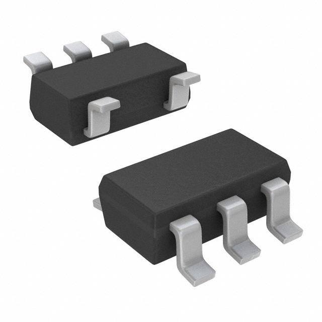
| 产品图片 |
|
| rohs | 符合RoHS无铅 / 符合限制有害物质指令(RoHS)规范要求 |
| 产品系列 | 放大器 IC,运算放大器 - 运放,Texas Instruments OPA379AIDCKT- |
| 数据手册 | |
| 产品型号 | OPA379AIDCKT |
| 产品目录页面 | |
| 产品种类 | 运算放大器 - 运放 |
| 供应商器件封装 | SC-70-5 |
| 共模抑制比—最小值 | 90 dB |
| 关闭 | No Shutdown |
| 其它名称 | 296-19875-2 |
| 包装 | 带卷 (TR) |
| 压摆率 | 0.03 V/µs |
| 商标 | Texas Instruments |
| 增益带宽生成 | 0.09 MHz |
| 增益带宽积 | 90kHz |
| 安装类型 | 表面贴装 |
| 安装风格 | SMD/SMT |
| 封装 | Reel |
| 封装/外壳 | 6-TSSOP(5 引线),SC-88A,SOT-353 |
| 封装/箱体 | SC-70-5 |
| 工作温度 | -40°C ~ 125°C |
| 工作电源电压 | 1.8 V to 5.5 V |
| 工厂包装数量 | 250 |
| 放大器类型 | 通用 |
| 最大工作温度 | + 125 C |
| 最小工作温度 | - 40 C |
| 标准包装 | 250 |
| 电压-电源,单/双 (±) | 1.8 V ~ 5.5 V, ±0.9 V ~ 2.75 V |
| 电压-输入失调 | 400µV |
| 电流-电源 | 2.9µA |
| 电流-输入偏置 | 5pA |
| 电流-输出/通道 | 5mA |
| 电源电流 | 2.9 uA |
| 电路数 | 1 |
| 系列 | OPA379 |
| 设计资源 | http://www.digikey.com/product-highlights/cn/zh/texas-instruments-webench-design-center/3176 |
| 转换速度 | 0.03 V/us |
| 输入偏压电流—最大 | 50 pA |
| 输入参考电压噪声 | 80 nV |
| 输入补偿电压 | 0.4 mV |
| 输出类型 | 满摆幅 |
| 通道数量 | 1 Channel |


- 商务部:美国ITC正式对集成电路等产品启动337调查
- 曝三星4nm工艺存在良率问题 高通将骁龙8 Gen1或转产台积电
- 太阳诱电将投资9.5亿元在常州建新厂生产MLCC 预计2023年完工
- 英特尔发布欧洲新工厂建设计划 深化IDM 2.0 战略
- 台积电先进制程称霸业界 有大客户加持明年业绩稳了
- 达到5530亿美元!SIA预计今年全球半导体销售额将创下新高
- 英特尔拟将自动驾驶子公司Mobileye上市 估值或超500亿美元
- 三星加码芯片和SET,合并消费电子和移动部门,撤换高东真等 CEO
- 三星电子宣布重大人事变动 还合并消费电子和移动部门
- 海关总署:前11个月进口集成电路产品价值2.52万亿元 增长14.8%


PDF Datasheet 数据手册内容提取
OPA379 OPA379 OPA2379 OPA4379 OPA2379 OPA4379 www.ti.com................................................................................................................................................... SBOS347D–NOVEMBER2005–REVISEDMAY2008 m 1.8V, 2.9 A, 90kHz, Rail-to-Rail I/O OPERATIONAL AMPLIFIERS FEATURES 1 DESCRIPTION • LOWNOISE:2.8m V (0.1Hz-10Hz) 2 PP • microPower:5.5m A(max) The OPA379 family of micropower, low-voltage operational amplifiers is designed for battery-powered • LOWOFFSETVOLTAGE:1.5mV(max) applications. These amplifiers operate on a supply • DCPRECISION: voltage as low as 1.8V (±0.9V). High-performance, – CMRR:100dB single-supply operation with rail-to-rail capability (10m V max) makes the OPA379 family useful for a – PSRR:2m V/V widerangeofapplications. – A :120dB OL InadditiontomicroSizepackages,theOPA379family • WIDESUPPLYVOLTAGERANGE:1.8Vto5.5V of op amps features impressive bandwidth (90kHz), • microSizePACKAGES: low bias current (5pA), and low noise (80nV/√Hz) – SC70-5,SOT23-5,SOT23-8,SO-8,TSSOP-14 relative to the very low quiescent current (5.5m A max). APPLICATIONS The OPA379 (single) is available in SC70-5, • BATTERY-POWEREDINSTRUMENTS SOT23-5, and SO-8 packages. The OPA2379 (dual) • PORTABLEDEVICES comes in SOT23-8 and SO-8 packages. The OPA4379 (quad) is offered in a TSSOP-14 package. • MEDICALINSTRUMENTS Allversionsarespecifiedfrom–40(cid:176) Cto+125(cid:176) C. • HANDHELDTESTEQUIPMENT xxx xxx xxx xxx xxx xxx xxx V S Table1.OPAx379RELATEDPRODUCTS FEATURES PRODUCT 1/2 OPA2379 C2 1m A,70kHz,2mVVOS,1.8Vto5.5VSupply OPAx349 C C1 R 1m A,5.5kHz,390m VVOS,2.5Vto16VSupply TLV240x S REF F 1m A,5.5kHz,0.6mVVOS,2.5Vto12VSupply TLV224x W R VS 7m A,160kHz,0.5mVVOS,2.7Vto16VSupply TLV27Lx B R 7m A,160kHz,0.5mVVOS,2.7Vto16VSupply TLV238x L R 1/2 20m A,350kHz,2mVVOS,2.3Vto5.5VSupply OPAx347 1 OPA2379 VOUT 20m A,500kHz,550m VVOS,1.8Vto3.6VSupply TLV276x 45m A,1MHz,1mVVOS,2.1Vto5.5VSupply OPAx348 R 1 Figure1.OPA2379inPortableGasMeter Application 1 Pleasebeawarethatanimportantnoticeconcerningavailability,standardwarranty,anduseincriticalapplicationsof TexasInstrumentssemiconductorproductsanddisclaimerstheretoappearsattheendofthisdatasheet. Alltrademarksarethepropertyoftheirrespectiveowners. 2 PRODUCTIONDATAinformationiscurrentasofpublicationdate. Copyright©2005–2008,TexasInstrumentsIncorporated Products conform to specifications per the terms of the Texas Instruments standard warranty. Production processing does not necessarilyincludetestingofallparameters.
OPA379 OPA2379 OPA4379 SBOS347D–NOVEMBER2005–REVISEDMAY2008................................................................................................................................................... www.ti.com This integrated circuit can be damaged by ESD. Texas Instruments recommends that all integrated circuits be handled with appropriateprecautions.Failuretoobserveproperhandlingandinstallationprocedurescancausedamage. ESDdamagecanrangefromsubtleperformancedegradationtocompletedevicefailure.Precisionintegratedcircuitsmaybemore susceptibletodamagebecauseverysmallparametricchangescouldcausethedevicenottomeetitspublishedspecifications. ABSOLUTE MAXIMUM RATINGS(1) Overoperatingfree-airtemperaturerange(unlessotherwisenoted). OPA379,OPA2379,OPA4379 UNIT SupplyVoltage V =(V+)–(V–) +7 V S SignalInputTerminals,Voltage(2) (V–)–0.5to(V+)+0.5 V SignalInputTerminals,Current(2) ±10 mA OutputShort-Circuit(3) Continuous OperatingTemperature T –40to+125 (cid:176) C A StorageTemperature T –65to+150 (cid:176) C A JunctionTemperature T +150 (cid:176) C J HumanBodyModel (HBM) 2000 V ESDRating ChargedDeviceModel (CDM) 1000 V (1) Stressesabovetheseratingsmaycausepermanentdamage.Exposuretoabsolutemaximumconditionsforextendedperiodsmay degradedevicereliability.Thesearestressratingsonly,andfunctionaloperationofthedeviceattheseoranyotherconditionsbeyond thosespecifiedisnotsupported. (2) Inputterminalsarediode-clampedtothepower-supplyrails.Inputsignalsthatcanswingmorethan0.5Vbeyondthesupplyrailsshould becurrent-limitedto10mAorless. (3) Short-circuittoground,oneamplifierperpackage. PACKAGE/ORDERINGINFORMATION(1) PRODUCT PACKAGE-LEAD PACKAGEDESIGNATOR PACKAGEMARKING SC70−5 DCK AYR OPA379 SOT23−5 DBV B53 SO−8 D OPA379A SOT23−8 DCN B61 OPA2379 SO−8 D OPA2379A OPA4379 TSSOP−14 PW OPA4379A (1) ForthemostcurrentpackageandorderinginformationseethePackageOptionAddendumattheendofthisdocument,orseetheTI websiteatwww.ti.com. 2 SubmitDocumentationFeedback Copyright©2005–2008,TexasInstrumentsIncorporated ProductFolderLink(s):OPA379OPA2379OPA4379
OPA379 OPA2379 OPA4379 www.ti.com................................................................................................................................................... SBOS347D–NOVEMBER2005–REVISEDMAY2008 PIN CONFIGURATIONS OPA379 OPA379 SC70-5 SOT23-5 (TOPVIEW) (TOPVIEW) +IN 1 5 V+ OUT 1 5 V+ V- 2 V- 2 -IN 3 4 OUT +IN 3 4 -IN OPA379 OPA2379(2) SO-8 SOT23-8 (TOPVIEW) (TOPVIEW) NC(1) 1 8 NC(1) OUT A 1 8 V+ -IN 2 7 V+ -IN 2 7 OUT B B 6 +IN 3 6 OUT +IN 3 1 6 -IN B V- 4 5 NC(1) V- 4 5 +IN B OPA2379 OPA4379 SO-8 TSSOP-14 (TOPVIEW) (TOPVIEW) OUT A 1 8 V+ OUT A 1 14 OUT D -IN A 2 7 OUT B -IN A 2 13 -IN D +IN A 3 6 -IN B +IN A 3 12 +IN D V- 4 5 +IN B V+ 4 11 V- +IN B 5 10 +IN C -IN B 6 9 -IN C OUT B 7 8 OUT C (1) NCdenotesnointernalconnection. (2) Pin 1 of the SOT23−8 package is determined by orienting the packagemarkingasshown. Copyright©2005–2008,TexasInstrumentsIncorporated SubmitDocumentationFeedback 3 ProductFolderLink(s):OPA379OPA2379OPA4379
OPA379 OPA2379 OPA4379 SBOS347D–NOVEMBER2005–REVISEDMAY2008................................................................................................................................................... www.ti.com ELECTRICAL CHARACTERISTICS: V = +1.8V to +5.5V S Boldfacelimitsapplyoverthespecifiedtemperaturerangeindicated. AtT =+25(cid:176) C,R =25kΩconnectedtoV /2,andV <(V+)–1V,unlessotherwisenoted. A L S CM OPA379,OPA2379,OPA4379 PARAMETER TESTCONDITIONS MIN TYP MAX UNIT OFFSETVOLTAGE InitialOffsetVoltage VOS VS=5V 0.4 1.5 mV Over–40(cid:176)Cto+125(cid:176)C 2 mV Drift,–40(cid:176)Cto+85(cid:176)C dVOS/dT 1.5 m V/(cid:176)C Drift,–40(cid:176)Cto+125(cid:176)C 2.7 m V/(cid:176)C vsPowerSupply PSRR 2 10 m V/V Over–40(cid:176)Cto+125(cid:176)C 20 m V/V INPUTVOLTAGERANGE Common-ModeVoltageRange VCM (V–)–0.1to(V+)+0.1 V Common-ModeRejectionRatio(1) CMRR (V–)<VCM<(V+)–1V 90 100 dB Over–40(cid:176)Cto+85(cid:176)C (V–)<VCM<(V+)–1V 80 dB Over–40(cid:176)Cto+125(cid:176)C (V–)<VCM<(V+)–1V 62 dB INPUTBIASCURRENT InputBiasCurrent IB VS=5V,VCM≤VS/2 ±5 ±50 pA InputOffsetCurrent IOS VS=5V ±5 ±50 pA INPUTIMPEDANCE Differential 1013||3 Ω||pF Common-Mode 1013||6 Ω||pF NOISE InputVoltageNoise f=0.1Hzto10Hz 2.8 m VPP InputVoltageNoiseDensity en f=1kHz 80 nV/√Hz InputCurrentNoiseDensity in f=1kHz 1 fA/√Hz OPEN-LOOPGAIN Open-LoopVoltageGain AOL VS=5V,RL=25kΩ,100mV<VO<(V+)–100mV 100 120 dB Over–40(cid:176)Cto+125(cid:176)C VS=5V,RL=25kΩ,100mV<VO<(V+)–100mV 80 dB VS=5V,RL=5kΩ,500mV<VO<(V+)–500mV 100 120 dB Over–40(cid:176)Cto+125(cid:176)C VS=5V,RL=5kΩ,500mV<VO<(V+)–500mV 80 dB OUTPUT VoltageOutputSwingfromRail RL=25kΩ 5 10 mV Over–40(cid:176)Cto+125(cid:176)C RL=25kΩ 15 mV RL=5kΩ 25 50 mV Over–40(cid:176)Cto+125(cid:176)C RL=5kΩ 75 mV Short-CircuitCurrent ISC ±5 mA CapacitiveLoadDrive CLOAD SeeTypicalCharacteristics Closed-LoopOutputImpedance ROUT G=1,f=1kHz,IO=0 10 Ω Open-LoopOutputImpedance RO f=100kHz,IO=0 28 kΩ FREQUENCYRESPONSE CLOAD=30pF GainBandwidthProduct GBW 90 kHz SlewRate SR G=+1 0.03 V/m s OverloadRecoveryTime VIN· GAIN>VS 25 m s Turn-OnTime tON 1 ms (1) SeeTypicalCharacteristicgragh,Common-ModeRejectionRatiovsFrequency(Figure3). 4 SubmitDocumentationFeedback Copyright©2005–2008,TexasInstrumentsIncorporated ProductFolderLink(s):OPA379OPA2379OPA4379
OPA379 OPA2379 OPA4379 www.ti.com................................................................................................................................................... SBOS347D–NOVEMBER2005–REVISEDMAY2008 ELECTRICAL CHARACTERISTICS: V = +1.8V to +5.5V (continued) S Boldfacelimitsapplyoverthespecifiedtemperaturerangeindicated. AtT =+25(cid:176) C,R =25kΩconnectedtoV /2,andV <(V+)–1V,unlessotherwisenoted. A L S CM OPA379,OPA2379,OPA4379 PARAMETER TESTCONDITIONS MIN TYP MAX UNIT POWERSUPPLY Specified/OperatingVoltageRange VS 1.8 5.5 V QuiescentCurrentperAmplifier IQ VS=5.5V,IO=0 2.9 5.5 m A Over–40(cid:176)Cto+125(cid:176)C 10 m A TEMPERATURE Specified/OperatingRange TA –40 +125 (cid:176)C StorageRange TJ –65 +150 (cid:176)C ThermalResistance q JA SC70−5 250 (cid:176)C/W SOT23−5 200 (cid:176)C/W SOT23−8,TSSOP−14,SO−8 150 (cid:176)C/W Copyright©2005–2008,TexasInstrumentsIncorporated SubmitDocumentationFeedback 5 ProductFolderLink(s):OPA379OPA2379OPA4379
OPA379 OPA2379 OPA4379 SBOS347D–NOVEMBER2005–REVISEDMAY2008................................................................................................................................................... www.ti.com TYPICAL CHARACTERISTICS AtT =+25(cid:176) C,V =5V,andR =25kΩconnectedtoV /2,unlessotherwisenoted. A S L S COMMON-MODEAND OPEN-LOOPGAINANDPHASE POWER-SUPPLYREJECTIONRATIO vsFREQUENCY vsFREQUENCY 120 0 120 100 -30 100 B) -PSRR d 80 -60 R ( 80 Gain (dB) 6400 --91020°Phase () RR and PSR 6400 +PSRR M C CMRR 20 -150 20 0 -180 0 0.1 1 10 100 1k 10k 100k 0.1 1 10 100 1k 10k 100k Frequency (Hz) Frequency (Hz) Figure2. Figure3. MAXIMUMOUTPUTVOLTAGE QUIESCENTCURRENT vsFREQUENCY vsSUPPLYVOLTAGE 5.0 3.5 4.5 4.0 put Voltage (V)PP 3322....5050 mscent Current (A) 32..05 Out 1.5 Quie 2.0 1.0 0.5 0 1.5 1k 10k 100k 1.5 2.0 2.5 3.0 3.5 4.0 4.5 5.0 5.5 Frequency (Hz) Supply Voltage (V) Figure4. Figure5. OUTPUTVOLTAGE SHORT-CIRCUITCURRENT vsOUTPUTCURRENT vsSUPPLYVOLTAGE 2.5 25 2.0 +I SC 11..50 VS=±2.5V nt (mA) 20 V(V)OUT -00..505 +125°C +85°C +25°C -40°C cuit Curre 15 -ISC Cir -1.0 ort- 10 -1.5 Sh -2.0 -2.5 5 0 1 2 3 4 5 6 7 8 9 10 1.5 2.0 2.5 3.0 3.5 4.0 4.5 5.0 5.5 I (mA) Supply Voltage (V) OUT Figure6. Figure7. 6 SubmitDocumentationFeedback Copyright©2005–2008,TexasInstrumentsIncorporated ProductFolderLink(s):OPA379OPA2379OPA4379
OPA379 OPA2379 OPA4379 www.ti.com................................................................................................................................................... SBOS347D–NOVEMBER2005–REVISEDMAY2008 TYPICAL CHARACTERISTICS (continued) AtT =+25(cid:176) C,V =5V,andR =25kΩconnectedtoV /2,unlessotherwisenoted. A S L S OFFSETVOLTAGEvsCOMMON-MODEVOLTAGE OFFSETVOLTAGE vsTEMPERATURE PRODUCTIONDISTRIBUTION 15.0 Unit 1 12.5 Common-Mode Input Range 10.0 7.5 V) CMRR Specified Range m 5.0 oltage ( 2.50 pulation set V --25..50 Po Off -7.5 -40°C -10.0 +85°C -12.5 +125°C Unit 2 -15.0 -0.5 0 0.5 1.0 1.5 2.0 2.5 3.0 3.5 4.0 4.5 5.0 5.5 00500050005000500050050005000500050005000 5320976431 1346790235 Common-Mode Voltage (V) -1-1-1-1------ 1111 Offset Voltage (mV) Figure8. Figure9. OFFSETVOLTAGEDRIFTDISTRIBUTION OFFSETVOLTAGEDRIFTDISTRIBUTION (–40(cid:176) Cto+85(cid:176) C) (–40(cid:176) Cto+125(cid:176) C) n n o o ati ati ul ul p p o o P P £1 £2 £3 £4 £5 > 5 £1 £2 £3 £4 £5 > 5 Offset Voltage Drift (mV/°C) Offset Voltage Drift (mV/°C) Figure10. Figure11. QUIESCENTCURRENT QUIESCENTCURRENT vsTEMPERATURE PRODUCTIONDISTRIBUTION 5.0 4.5 4.0 3.5 n o A) ati (m 3.0 pul Q o I 2.5 P 2.0 1.5 1.0 -50 -25 0 25 50 75 100 125 1.01.21.41.61.82.02.22.42.62.83.03.23.43.63.84.04.24.44.64.85.0 Temperature (°C) Quiescent Current (mA) Figure12. Figure13. Copyright©2005–2008,TexasInstrumentsIncorporated SubmitDocumentationFeedback 7 ProductFolderLink(s):OPA379OPA2379OPA4379
OPA379 OPA2379 OPA4379 SBOS347D–NOVEMBER2005–REVISEDMAY2008................................................................................................................................................... www.ti.com TYPICAL CHARACTERISTICS (continued) AtT =+25(cid:176) C,V =5V,andR =25kΩconnectedtoV /2,unlessotherwisenoted. A S L S INPUTBIASCURRENT vsTEMPERATURE 0.1HzTO10HzNOISE 10000 1000 A) p nt ( 100 Curre 10 V/div as 1m Bi ut 1 p n I 0.1 0.01 -50 -25 0 25 50 75 100 125 2.5s/div Temperature (°C) Figure14. Figure15. SMALL-SIGNALOVERSHOOT NOISEvsFREQUENCY vsCAPACITIVELOAD 1000 60 50 )Hz %) 40 Öse (nV/ 100 ershoot ( 30 G = +1 Noi Ov 20 10 G =-1 10 0 1 10 100 1k 10k 10 100 1000 Frequency (Hz) Capacitive Load (pF) Figure16. Figure17. SMALL-SIGNALSTEPRESPONSE LARGE-SIGNALSTEPRESPONSE mV/div mV/div 20 500 25ms/div 50ms/div Figure18. Figure19. 8 SubmitDocumentationFeedback Copyright©2005–2008,TexasInstrumentsIncorporated ProductFolderLink(s):OPA379OPA2379OPA4379
OPA379 OPA2379 OPA4379 www.ti.com................................................................................................................................................... SBOS347D–NOVEMBER2005–REVISEDMAY2008 APPLICATION INFORMATION The OPA379 family of operational amplifiers minimizes power consumption without compromising V bandwidth or noise. Power-supply rejection ratio S (PSRR), common-mode rejection ratio (CMRR), and I OVERLOAD open-loop gain (A ) typical values are 100dB or 10mA max OL OPA379 V OUT better. V IN 5kW When designing for ultra-low power, choose system components carefully. To minimize current consumption, select large-value resistors. Any Figure20.InputCurrentProtectionforVoltages resistors will react with stray capacitance in the circuit ExceedingtheSupplyVoltage and the input capacitance of the operational amplifier. These parasitic RC combinations can affect the stability of the overall system. A feedback capacitor NOISE may be required to assure stability and limit overshootorgainpeaking. Although micropower amplifiers frequently have high wideband noise, the OPA379 series offer excellent Good layout practice mandates the use of a 0.1m F noise performance. Resistors should be chosen bypass capacitor placed closely across the supply carefully because the OPA379 has only 2.8m V of PP pins. 0.1Hz to 10Hz noise, and 80nV/√Hz of wideband noise; otherwise, they can become the dominant OPERATING VOLTAGE sourceofnoise. OPA379seriesopampsarefully specified and tested CAPACITIVE LOAD AND STABILITY from +1.8V to +5.5V (±0.9V to ±2.75V). Parameters that will vary with supply voltage are shown in the Follower configurations with load capacitance in TypicalCharacteristicscurves. excess of 30pF can produce extra overshoot (see typical characteristic Small-Signal Overshoot vs INPUT COMMON-MODE VOLTAGE RANGE Capacitive Load, Figure 17) and ringing in the output signal. Increasing the gain enhances the ability of the The input common-mode voltage range of the amplifier to drive greater capacitive loads. In OPA379 family typically extends 100mV beyond each unity-gain configurations, capacitive load drive can be supply rail. This rail-to-rail input is achieved using a improved by inserting a small (10Ω to 20Ω) resistor, complementary input stage. CMRR is specified from R , in series with the output, as shown in Figure 21. the negative rail to 1V below the positive rail. S This resistor significantly reduces ringing while Between (V+) – 1V and (V+) + 0.1V, the amplifier maintaining direct current (dc) performance for purely operates with higher offset voltage because of the capacitive loads. However, if there is a resistive load transition region of the input stage. See the typical inparallelwith the capacitive load, a voltage divider is characteristic, Offset Voltage vs Common-Mode created, introducing a dc error at the output and VoltagevsTemperature(Figure8). slightly reducing the output swing. The error introduced is proportional to the ratio R /R , and is PROTECTING INPUTS FROM S L generallynegligible. OVER-VOLTAGE Normally, input currents are 5pA. However, a large voltage input (greater than 500mV beyond the supply VS rails) can cause excessive current to flow in or out of R the input pins. Therefore, as well as keeping the input S OPA379 V voltagebelowthemaximumrating,it is also important OUT V 10Wto to limit the input current to less than 10mA. This IN 20W RL CL limiting is easily accomplished with an input voltage resistor,asshowninFigure20. Figure21.SeriesResistorinUnity-GainBuffer ConfigurationImprovesCapacitiveLoadDrive Copyright©2005–2008,TexasInstrumentsIncorporated SubmitDocumentationFeedback 9 ProductFolderLink(s):OPA379OPA2379OPA4379
OPA379 OPA2379 OPA4379 SBOS347D–NOVEMBER2005–REVISEDMAY2008................................................................................................................................................... www.ti.com In unity-gain inverter configuration, phase margin can V R = REF be reduced by the reaction between the capacitance F 1000(I ) at the op amp input and the gain setting resistors. BMAX Best performance is achieved by using smaller 1.2V = valued resistors. However, when large valued 1000(100pA) resistors cannot be avoided, a small (4pF to 6pF) capacitor, C , can be inserted in the feedback, as = 12MW»10MW (1) FB shown in Figure 22. This configuration significantly 2. Choose the hysteresis voltage, V . For battery HYST reduces overshoot by compensating the effect of monitoringapplications,50mVisadequate. capacitance, CIN, which includes the amplifier input 3. CalculateR1asfollows: capacitance (3pf) and printed circuit board (PC) V 50mW parasiticcapacitance. R = R HYST = 10MW = 210kW 1 F V 2.4V BATT (2) C FB 4. Select a threshold voltage for V rising (V ) = IN THRS 2.0V R F 5. CalculateR asfollows: 2 1 R R = V IN 2 IN V 1 1 OPA379 V THRS - - OUT C V ´R R R IN REF 1 1 F 1 = 2V 1 1 Figure22.ImprovingStabilityforLargeR andR - - F IN 1.2V´210kW 210kW 10MW BATTERY MONITORING = 325kW (3) The low operating voltage and quiescent current of 6. Calculate R : The minimum supply voltage for BIAS the OPA379 series make it an excellent choice for this circuit is 1.8V. The REF1112 has a current battery monitoring applications, as shown in requirement of 1.2m A (max). Providing 2m A of Figure 23. In this circuit, VSTATUS is high as long as supply current assures proper operation. the battery voltage remains above 2V. A low-power Therefore: reference is used to set the trip point. Resistor values (V -V ) (1.8V-1.2V) areselectedasfollows: R = BATTMIN REF = = 0.3MW BIAS I 2mA 1. R Selecting: Select R such that the current BIAS (4) F F through R is approximately 1000x larger than F themaximumbiascurrentovertemperature: R F R 1 +IN + I OUT V BIAS OPA379 V BATT -IN STATUS R BIAS V R REF 2 REF1112 Figure23.BatteryMonitor 10 SubmitDocumentationFeedback Copyright©2005–2008,TexasInstrumentsIncorporated ProductFolderLink(s):OPA379OPA2379OPA4379
OPA379 OPA2379 OPA4379 www.ti.com................................................................................................................................................... SBOS347D–NOVEMBER2005–REVISEDMAY2008 WINDOW COMPARATOR The window comparator threshold voltages are set as follows: Figure 24 shows the OPA2379 used as a window R comparator. The threshold limits are set by VH and V = 2 ´V V , with V > V . When V < V , the output of A1 is H R + R S L H L IN H 1 2 (5) low. When V > V , the output of A2 is low. IN L R Therefore, both op amp outputs are at 0V as long as V = 4 ´V V is between V and V . This architecture results in L R + R S IN H L 3 4 (6) no current flowing through either diode, Q1 in cutoff, withthebasevoltageat0V,andV forcedhigh. OUT If V falls below V , the output of A2 is high, current IN L flows through D2, and V is low. Likewise, if V OUT IN rises above V , the output of A1 is high, current flows H throughD1,andV islow. OUT V S V S R 1 V H A1 D1(2) 1/2 V OPA2379 S R 2 R 7 5.1kW RIN R VOUT 2kW(1) 10k5W VIN Q1(3) R 6 V 5.1kW V S S A2 D2(2) R 1/2 3 OPA2379 V L R 4 (1) R protectsA1andA2frompossibleexcesscurrentflow. IN (2) IN4446orequivalentdiodes. (3) 2N2222orequivalentNPNtransistor. Figure24.OPA2379asaWindowComparator Copyright©2005–2008,TexasInstrumentsIncorporated SubmitDocumentationFeedback 11 ProductFolderLink(s):OPA379OPA2379OPA4379
OPA379 OPA2379 OPA4379 SBOS347D–NOVEMBER2005–REVISEDMAY2008................................................................................................................................................... www.ti.com ADDITIONAL APPLICATION EXAMPLES Figure25throughFigure29illustrateadditionalapplicationexamples. +2.7V R R 3 2 V CC +2.7V MSP430x20x3PW R 1 66.5W A0+ 16-Bit OPA379 VIN C1 ADC 1.5nF REF3312 VREF C V 2 SS 1mF Figure25.UnipolarSignalChainConfiguration V EX R 1 V S R R R R OPA379 V OUT R 1 V REF Figure26.SingleOpAmpBridgeAmplifier 3V +5V REF3130 Load R R 1 2 4.99kW 49.9kW R V 716.5kW 5R6NW ILOAD R1WSHUNT OPA379 R3 R4 ADS1100 RN I2C 4.99kW 48.7kW 56W Stray Ground-Loop Resistance R7 (PGA Gain = 4) 1.18kW FS = 3.0V NOTE:1%resistorsprovideadequatecommon-moderejectionatsmallground-looperrors. Figure27.Low-SideCurrentMonitor 12 SubmitDocumentationFeedback Copyright©2005–2008,TexasInstrumentsIncorporated ProductFolderLink(s):OPA379OPA2379OPA4379
OPA379 OPA2379 OPA4379 www.ti.com................................................................................................................................................... SBOS347D–NOVEMBER2005–REVISEDMAY2008 R G zener(1) R V+ SHUNT R1(2) MOSFET rated to 10kW OPA379 stand-off supply voltage such as BSS84 for V- up to 50V. +5V Two zener biasing methods are shown.(3) Output Load R BIAS R L (1) Zenerratedforopampsupplycapability(thatis,5.1VforOPA379). (2) Current-limitingresistor. (3) ChoosezenerbiasingresistorordualNMOSMETs(FDG6301N,NTJD4001N,orSi1034). Figure28.High-SideCurrentMonitor R G VREF R1 R2 R2 R1 VOUT 1/2 1/2 V OPA2379 OPA2379 2 V 1 R 2R V =(V -V) 1 + 1 + 1 + V OUT 1 2 R R REF 2 G Figure29.TwoOpAmpInstrumentationAmplifier Copyright©2005–2008,TexasInstrumentsIncorporated SubmitDocumentationFeedback 13 ProductFolderLink(s):OPA379OPA2379OPA4379
PACKAGE OPTION ADDENDUM www.ti.com 6-Feb-2020 PACKAGING INFORMATION Orderable Device Status Package Type Package Pins Package Eco Plan Lead/Ball Finish MSL Peak Temp Op Temp (°C) Device Marking Samples (1) Drawing Qty (2) (6) (3) (4/5) OPA2379AID ACTIVE SOIC D 8 75 Green (RoHS NIPDAU Level-2-260C-1 YEAR -40 to 125 2379A & no Sb/Br) OPA2379AIDCNR ACTIVE SOT-23 DCN 8 3000 Green (RoHS NIPDAU Level-2-260C-1 YEAR -40 to 125 BPK & no Sb/Br) OPA2379AIDCNT ACTIVE SOT-23 DCN 8 250 Green (RoHS NIPDAU Level-2-260C-1 YEAR -40 to 125 BPK & no Sb/Br) OPA2379AIDG4 ACTIVE SOIC D 8 75 Green (RoHS NIPDAU Level-2-260C-1 YEAR -40 to 125 2379A & no Sb/Br) OPA2379AIDR ACTIVE SOIC D 8 2500 Green (RoHS NIPDAU Level-2-260C-1 YEAR -40 to 125 2379A & no Sb/Br) OPA2379AIDRG4 ACTIVE SOIC D 8 2500 Green (RoHS NIPDAU Level-2-260C-1 YEAR -40 to 125 2379A & no Sb/Br) OPA379AID ACTIVE SOIC D 8 75 Green (RoHS NIPDAU Level-2-260C-1 YEAR -40 to 125 OPA & no Sb/Br) 379A OPA379AIDBVR ACTIVE SOT-23 DBV 5 3000 Green (RoHS NIPDAU Level-2-260C-1 YEAR -40 to 125 B53 & no Sb/Br) OPA379AIDBVRG4 ACTIVE SOT-23 DBV 5 3000 Green (RoHS NIPDAU Level-2-260C-1 YEAR -40 to 125 B53 & no Sb/Br) OPA379AIDBVT ACTIVE SOT-23 DBV 5 250 Green (RoHS NIPDAU Level-2-260C-1 YEAR -40 to 125 B53 & no Sb/Br) OPA379AIDBVTG4 ACTIVE SOT-23 DBV 5 250 Green (RoHS NIPDAU Level-2-260C-1 YEAR -40 to 125 B53 & no Sb/Br) OPA379AIDCKR ACTIVE SC70 DCK 5 3000 Green (RoHS NIPDAU Level-2-260C-1 YEAR -40 to 125 B54 & no Sb/Br) OPA379AIDCKT ACTIVE SC70 DCK 5 250 Green (RoHS NIPDAU Level-2-260C-1 YEAR -40 to 125 B54 & no Sb/Br) OPA379AIDCKTG4 ACTIVE SC70 DCK 5 250 Green (RoHS NIPDAU Level-2-260C-1 YEAR -40 to 125 B54 & no Sb/Br) OPA379AIDR ACTIVE SOIC D 8 2500 Green (RoHS NIPDAU Level-2-260C-1 YEAR -40 to 125 OPA & no Sb/Br) 379A OPA379AIDRG4 ACTIVE SOIC D 8 2500 Green (RoHS NIPDAU Level-2-260C-1 YEAR -40 to 125 OPA & no Sb/Br) 379A OPA4379AIPWR ACTIVE TSSOP PW 14 2000 Green (RoHS NIPDAU Level-2-260C-1 YEAR -40 to 125 4379A & no Sb/Br) Addendum-Page 1
PACKAGE OPTION ADDENDUM www.ti.com 6-Feb-2020 (1) The marketing status values are defined as follows: ACTIVE: Product device recommended for new designs. LIFEBUY: TI has announced that the device will be discontinued, and a lifetime-buy period is in effect. NRND: Not recommended for new designs. Device is in production to support existing customers, but TI does not recommend using this part in a new design. PREVIEW: Device has been announced but is not in production. Samples may or may not be available. OBSOLETE: TI has discontinued the production of the device. (2) RoHS: TI defines "RoHS" to mean semiconductor products that are compliant with the current EU RoHS requirements for all 10 RoHS substances, including the requirement that RoHS substance do not exceed 0.1% by weight in homogeneous materials. Where designed to be soldered at high temperatures, "RoHS" products are suitable for use in specified lead-free processes. TI may reference these types of products as "Pb-Free". RoHS Exempt: TI defines "RoHS Exempt" to mean products that contain lead but are compliant with EU RoHS pursuant to a specific EU RoHS exemption. Green: TI defines "Green" to mean the content of Chlorine (Cl) and Bromine (Br) based flame retardants meet JS709B low halogen requirements of <=1000ppm threshold. Antimony trioxide based flame retardants must also meet the <=1000ppm threshold requirement. (3) MSL, Peak Temp. - The Moisture Sensitivity Level rating according to the JEDEC industry standard classifications, and peak solder temperature. (4) There may be additional marking, which relates to the logo, the lot trace code information, or the environmental category on the device. (5) Multiple Device Markings will be inside parentheses. Only one Device Marking contained in parentheses and separated by a "~" will appear on a device. If a line is indented then it is a continuation of the previous line and the two combined represent the entire Device Marking for that device. (6) Lead/Ball Finish - Orderable Devices may have multiple material finish options. Finish options are separated by a vertical ruled line. Lead/Ball Finish values may wrap to two lines if the finish value exceeds the maximum column width. Important Information and Disclaimer:The information provided on this page represents TI's knowledge and belief as of the date that it is provided. TI bases its knowledge and belief on information provided by third parties, and makes no representation or warranty as to the accuracy of such information. Efforts are underway to better integrate information from third parties. TI has taken and continues to take reasonable steps to provide representative and accurate information but may not have conducted destructive testing or chemical analysis on incoming materials and chemicals. TI and TI suppliers consider certain information to be proprietary, and thus CAS numbers and other limited information may not be available for release. In no event shall TI's liability arising out of such information exceed the total purchase price of the TI part(s) at issue in this document sold by TI to Customer on an annual basis. Addendum-Page 2
PACKAGE MATERIALS INFORMATION www.ti.com 3-Aug-2017 TAPE AND REEL INFORMATION *Alldimensionsarenominal Device Package Package Pins SPQ Reel Reel A0 B0 K0 P1 W Pin1 Type Drawing Diameter Width (mm) (mm) (mm) (mm) (mm) Quadrant (mm) W1(mm) OPA2379AIDCNR SOT-23 DCN 8 3000 179.0 8.4 3.2 3.2 1.4 4.0 8.0 Q3 OPA2379AIDCNT SOT-23 DCN 8 250 179.0 8.4 3.2 3.2 1.4 4.0 8.0 Q3 OPA2379AIDR SOIC D 8 2500 330.0 12.4 6.4 5.2 2.1 8.0 12.0 Q1 OPA379AIDBVR SOT-23 DBV 5 3000 178.0 9.0 3.3 3.2 1.4 4.0 8.0 Q3 OPA379AIDBVT SOT-23 DBV 5 250 178.0 9.0 3.3 3.2 1.4 4.0 8.0 Q3 OPA379AIDCKR SC70 DCK 5 3000 179.0 8.4 2.2 2.5 1.2 4.0 8.0 Q3 OPA379AIDCKR SC70 DCK 5 3000 178.0 9.0 2.4 2.5 1.2 4.0 8.0 Q3 OPA379AIDCKT SC70 DCK 5 250 178.0 9.0 2.4 2.5 1.2 4.0 8.0 Q3 OPA379AIDCKT SC70 DCK 5 250 179.0 8.4 2.2 2.5 1.2 4.0 8.0 Q3 OPA379AIDR SOIC D 8 2500 330.0 12.4 6.4 5.2 2.1 8.0 12.0 Q1 OPA4379AIPWR TSSOP PW 14 2000 330.0 12.4 6.9 5.6 1.6 8.0 12.0 Q1 PackMaterials-Page1
PACKAGE MATERIALS INFORMATION www.ti.com 3-Aug-2017 *Alldimensionsarenominal Device PackageType PackageDrawing Pins SPQ Length(mm) Width(mm) Height(mm) OPA2379AIDCNR SOT-23 DCN 8 3000 195.0 200.0 45.0 OPA2379AIDCNT SOT-23 DCN 8 250 195.0 200.0 45.0 OPA2379AIDR SOIC D 8 2500 367.0 367.0 35.0 OPA379AIDBVR SOT-23 DBV 5 3000 180.0 180.0 18.0 OPA379AIDBVT SOT-23 DBV 5 250 180.0 180.0 18.0 OPA379AIDCKR SC70 DCK 5 3000 195.0 200.0 45.0 OPA379AIDCKR SC70 DCK 5 3000 190.0 190.0 30.0 OPA379AIDCKT SC70 DCK 5 250 190.0 190.0 30.0 OPA379AIDCKT SC70 DCK 5 250 195.0 200.0 45.0 OPA379AIDR SOIC D 8 2500 367.0 367.0 35.0 OPA4379AIPWR TSSOP PW 14 2000 367.0 367.0 35.0 PackMaterials-Page2
None
None
PACKAGE OUTLINE DBV0005A SOT-23 - 1.45 mm max height SCALE 4.000 SMALL OUTLINE TRANSISTOR C 3.0 2.6 0.1 C 1.75 1.45 1.45 B A 0.90 PIN 1 INDEX AREA 1 5 2X 0.95 3.05 2.75 1.9 1.9 2 4 3 0.5 5X 0.3 0.15 0.2 C A B (1.1) TYP 0.00 0.25 GAGE PLANE 0.22 TYP 0.08 8 TYP 0.6 0 0.3 TYP SEATING PLANE 4214839/E 09/2019 NOTES: 1. All linear dimensions are in millimeters. Any dimensions in parenthesis are for reference only. Dimensioning and tolerancing per ASME Y14.5M. 2. This drawing is subject to change without notice. 3. Refernce JEDEC MO-178. 4. Body dimensions do not include mold flash, protrusions, or gate burrs. Mold flash, protrusions, or gate burrs shall not exceed 0.15 mm per side. www.ti.com
EXAMPLE BOARD LAYOUT DBV0005A SOT-23 - 1.45 mm max height SMALL OUTLINE TRANSISTOR PKG 5X (1.1) 1 5 5X (0.6) SYMM (1.9) 2 2X (0.95) 3 4 (R0.05) TYP (2.6) LAND PATTERN EXAMPLE EXPOSED METAL SHOWN SCALE:15X SOLDER MASK SOLDER MASK METAL UNDER METAL OPENING OPENING SOLDER MASK EXPOSED METAL EXPOSED METAL 0.07 MAX 0.07 MIN ARROUND ARROUND NON SOLDER MASK SOLDER MASK DEFINED DEFINED (PREFERRED) SOLDER MASK DETAILS 4214839/E 09/2019 NOTES: (continued) 5. Publication IPC-7351 may have alternate designs. 6. Solder mask tolerances between and around signal pads can vary based on board fabrication site. www.ti.com
EXAMPLE STENCIL DESIGN DBV0005A SOT-23 - 1.45 mm max height SMALL OUTLINE TRANSISTOR PKG 5X (1.1) 1 5 5X (0.6) SYMM 2 (1.9) 2X(0.95) 3 4 (R0.05) TYP (2.6) SOLDER PASTE EXAMPLE BASED ON 0.125 mm THICK STENCIL SCALE:15X 4214839/E 09/2019 NOTES: (continued) 7. Laser cutting apertures with trapezoidal walls and rounded corners may offer better paste release. IPC-7525 may have alternate design recommendations. 8. Board assembly site may have different recommendations for stencil design. www.ti.com
None
None
PACKAGE OUTLINE D0008A SOIC - 1.75 mm max height SCALE 2.800 SMALL OUTLINE INTEGRATED CIRCUIT C SEATING PLANE .228-.244 TYP [5.80-6.19] .004 [0.1] C A PIN 1 ID AREA 6X .050 [1.27] 8 1 2X .189-.197 [4.81-5.00] .150 NOTE 3 [3.81] 4X (0 -15 ) 4 5 8X .012-.020 B .150-.157 [0.31-0.51] .069 MAX [3.81-3.98] .010 [0.25] C A B [1.75] NOTE 4 .005-.010 TYP [0.13-0.25] 4X (0 -15 ) SEE DETAIL A .010 [0.25] .004-.010 0 - 8 [0.11-0.25] .016-.050 [0.41-1.27] DETAIL A (.041) TYPICAL [1.04] 4214825/C 02/2019 NOTES: 1. Linear dimensions are in inches [millimeters]. Dimensions in parenthesis are for reference only. Controlling dimensions are in inches. Dimensioning and tolerancing per ASME Y14.5M. 2. This drawing is subject to change without notice. 3. This dimension does not include mold flash, protrusions, or gate burrs. Mold flash, protrusions, or gate burrs shall not exceed .006 [0.15] per side. 4. This dimension does not include interlead flash. 5. Reference JEDEC registration MS-012, variation AA. www.ti.com
EXAMPLE BOARD LAYOUT D0008A SOIC - 1.75 mm max height SMALL OUTLINE INTEGRATED CIRCUIT 8X (.061 ) [1.55] SYMM SEE DETAILS 1 8 8X (.024) [0.6] SYMM (R.002 ) TYP [0.05] 5 4 6X (.050 ) [1.27] (.213) [5.4] LAND PATTERN EXAMPLE EXPOSED METAL SHOWN SCALE:8X SOLDER MASK SOLDER MASK METAL OPENING OPENING METAL UNDER SOLDER MASK EXPOSED METAL EXPOSED METAL .0028 MAX .0028 MIN [0.07] [0.07] ALL AROUND ALL AROUND NON SOLDER MASK SOLDER MASK DEFINED DEFINED SOLDER MASK DETAILS 4214825/C 02/2019 NOTES: (continued) 6. Publication IPC-7351 may have alternate designs. 7. Solder mask tolerances between and around signal pads can vary based on board fabrication site. www.ti.com
EXAMPLE STENCIL DESIGN D0008A SOIC - 1.75 mm max height SMALL OUTLINE INTEGRATED CIRCUIT 8X (.061 ) [1.55] SYMM 1 8 8X (.024) [0.6] SYMM (R.002 ) TYP [0.05] 5 4 6X (.050 ) [1.27] (.213) [5.4] SOLDER PASTE EXAMPLE BASED ON .005 INCH [0.125 MM] THICK STENCIL SCALE:8X 4214825/C 02/2019 NOTES: (continued) 8. Laser cutting apertures with trapezoidal walls and rounded corners may offer better paste release. IPC-7525 may have alternate design recommendations. 9. Board assembly site may have different recommendations for stencil design. www.ti.com
None
None
IMPORTANTNOTICEANDDISCLAIMER TI PROVIDES TECHNICAL AND RELIABILITY DATA (INCLUDING DATASHEETS), DESIGN RESOURCES (INCLUDING REFERENCE DESIGNS), APPLICATION OR OTHER DESIGN ADVICE, WEB TOOLS, SAFETY INFORMATION, AND OTHER RESOURCES “AS IS” AND WITH ALL FAULTS, AND DISCLAIMS ALL WARRANTIES, EXPRESS AND IMPLIED, INCLUDING WITHOUT LIMITATION ANY IMPLIED WARRANTIES OF MERCHANTABILITY, FITNESS FOR A PARTICULAR PURPOSE OR NON-INFRINGEMENT OF THIRD PARTY INTELLECTUAL PROPERTY RIGHTS. These resources are intended for skilled developers designing with TI products. You are solely responsible for (1) selecting the appropriate TI products for your application, (2) designing, validating and testing your application, and (3) ensuring your application meets applicable standards, and any other safety, security, or other requirements. These resources are subject to change without notice. TI grants you permission to use these resources only for development of an application that uses the TI products described in the resource. Other reproduction and display of these resources is prohibited. No license is granted to any other TI intellectual property right or to any third party intellectual property right. TI disclaims responsibility for, and you will fully indemnify TI and its representatives against, any claims, damages, costs, losses, and liabilities arising out of your use of these resources. TI’s products are provided subject to TI’s Terms of Sale (www.ti.com/legal/termsofsale.html) or other applicable terms available either on ti.com or provided in conjunction with such TI products. TI’s provision of these resources does not expand or otherwise alter TI’s applicable warranties or warranty disclaimers for TI products. Mailing Address: Texas Instruments, Post Office Box 655303, Dallas, Texas 75265 Copyright © 2020, Texas Instruments Incorporated