ICGOO在线商城 > 集成电路(IC) > 数据采集 - 模数转换器 > AD7685ACPZRL7
 Datasheet下载
- 型号: AD7685ACPZRL7
- 制造商: Analog
- 库位|库存: xxxx|xxxx
- 要求:
| 数量阶梯 | 香港交货 | 国内含税 |
| +xxxx | $xxxx | ¥xxxx |
查看当月历史价格
查看今年历史价格
AD7685ACPZRL7产品简介:
ICGOO电子元器件商城为您提供AD7685ACPZRL7由Analog设计生产,在icgoo商城现货销售,并且可以通过原厂、代理商等渠道进行代购。 AD7685ACPZRL7价格参考¥80.00-¥104.25。AnalogAD7685ACPZRL7封装/规格:数据采集 - 模数转换器, 16 Bit Analog to Digital Converter 1 Input 1 SAR 10-LFCSP-WD (3x3)。您可以下载AD7685ACPZRL7参考资料、Datasheet数据手册功能说明书,资料中有AD7685ACPZRL7 详细功能的应用电路图电压和使用方法及教程。
AD7685ACPZRL7是由Analog Devices Inc.(亚德诺半导体公司)生产的一款16位、逐次逼近寄存器(SAR)型模数转换器(ADC)。该器件具有高速、低功耗的特点,适用于多种数据采集应用场景。

 应用场景

1. 工业自动化与控制
   AD7685ACPZRL7在工业自动化领域中广泛应用。它能够精确地将模拟信号(如传感器输出的电压或电流)转换为数字信号,供微控制器或处理器处理。例如,在温度、压力、流量等传感器的数据采集系统中,AD7685可以提供高精度的测量结果,确保控制系统能够做出准确的响应。

2. 医疗设备
   在医疗设备中,AD7685ACPZRL7用于心电图(ECG)、脑电图(EEG)、超声波成像等设备中的信号采集。这些设备需要高分辨率和快速响应的ADC来捕捉生物电信号的变化,AD7685的16位分辨率和低噪声特性使其成为理想选择。

3. 电力监测与保护
   电力系统中的电压、电流监测需要高精度的ADC。AD7685ACPZRL7可以用于电力监控设备中,实时采集电网参数,帮助检测异常情况并采取保护措施。其低功耗特性也使得它适合长时间运行的电力监测系统。

4. 通信设备
   在通信基站、无线电接收机等设备中,AD7685ACPZRL7用于射频(RF)信号的数字化处理。它能够快速而准确地将接收到的模拟信号转换为数字信号,以便进一步处理和传输。

5. 环境监测
   环境监测系统通常需要采集大量的传感器数据,如空气质量、水质、土壤湿度等。AD7685ACPZRL7的高精度和多通道能力使其非常适合这类应用,能够在不同环境下稳定工作,提供可靠的测量结果。

6. 汽车电子
   在汽车电子系统中,AD7685ACPZRL7可用于电池管理系统(BMS)、车载传感器数据采集等。它能够实时监测电池状态和其他关键参数,确保车辆的安全性和可靠性。

总之,AD7685ACPZRL7凭借其高精度、低功耗和快速响应的特点,广泛应用于各种对数据采集有严格要求的领域,确保系统的稳定性和准确性。
| 参数 | 数值 |
| 产品目录 | 集成电路 (IC) |
| 描述 | IC ADC 16BIT SAR 250KSPS 10LFCSP |
| 产品分类 | |
| 品牌 | Analog Devices Inc |
| 数据手册 | |
| 产品图片 |
|
| 产品型号 | AD7685ACPZRL7 |
| rohs | 无铅 / 符合限制有害物质指令(RoHS)规范要求 |
| 产品系列 | PulSAR® |
| 产品培训模块 | http://www.digikey.cn/PTM/IndividualPTM.page?site=cn&lang=zhs&ptm=18570 |
| 位数 | 16 |
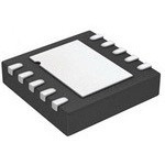
| 供应商器件封装 | 10-LFCSP-WD(3x3) |
| 其它名称 | AD7685ACPZRL7CT |
| 包装 | 带卷 (TR) |
| 安装类型 | 表面贴装 |
| 封装/外壳 | 10-WFDFN 裸露焊盘,CSP |
| 工作温度 | -40°C ~ 85°C |
| 数据接口 | DSP,MICROWIRE™,QSPI™,串行,SPI™ |
| 标准包装 | 1 |
| 特性 | - |
| 电压源 | 单电源 |
| 设计资源 | |
| 转换器数 | 1 |
| 输入数和类型 | 1 个伪差分,单极 |
| 配用 | /product-detail/zh/EVAL-AD7685-PMDZ/EVAL-AD7685-PMDZ-ND/4875922 |
| 采样率(每秒) | 250k |


- 商务部:美国ITC正式对集成电路等产品启动337调查
- 曝三星4nm工艺存在良率问题 高通将骁龙8 Gen1或转产台积电
- 太阳诱电将投资9.5亿元在常州建新厂生产MLCC 预计2023年完工
- 英特尔发布欧洲新工厂建设计划 深化IDM 2.0 战略
- 台积电先进制程称霸业界 有大客户加持明年业绩稳了
- 达到5530亿美元!SIA预计今年全球半导体销售额将创下新高
- 英特尔拟将自动驾驶子公司Mobileye上市 估值或超500亿美元
- 三星加码芯片和SET,合并消费电子和移动部门,撤换高东真等 CEO
- 三星电子宣布重大人事变动 还合并消费电子和移动部门
- 海关总署:前11个月进口集成电路产品价值2.52万亿元 增长14.8%


PDF Datasheet 数据手册内容提取
16-Bit, 250 kSPS PulSAR ADC in MSOP Data Sheet AD7685 FEATURES TYPICAL APPLICATION CIRCUIT 16-bit resolution with no missing codes 0.5VTO VDD 2.5VTO 5V Throughput: 250 kSPS INL: ±0.6 LSB typical, ±2 LSB maximum (±0.003% of FSR) SINAD: 93.5 dB at 20 kHz REF VDD VIO 1.8VTO VDD 0TO VREF THD: −110 dB at 20 kHz SDI IN+ Pseudo differential analog input range AD7685SCK 3- OR 4-WIRE INTERFACE IN– SDO (SPI, DAISY CHAIN, CS) 0 V to V with V up to VDD REF REF GND CNV No pipeline delay Sin1g.8le V-s tuop 5p Vly l oopgeicr aintitoenrf 2ac.3e V to 5.5 V with 02968-001 Figure 2. Proprietary serial interface: SPI-/QSPI™-/MICROWIRE™-/DSP- compatible Table 1. MSOP, LFCSP/SOT-23 14-/16-/18-Bit PulSAR ADC Daisy-chain multiple ADCs, BUSY indicator 400 kSPS Power dissipation 100 250 to 1000 ADC Type kSPS kSPS 500 kSPS kSPS Driver 1.4 µW at 2.5 V/100 SPS 18-Bit True AD7691 AD7690 AD7982 ADA4941 1.35 mW at 2.5 V/100 kSPS, 4 mW at 5 V/100 kSPS Differential AD7982 ADA4841 Standby current: 1 nA 16-Bit True AD7684 AD7687 AD7688 ADA4941 10-lead package: MSOP (MSOP-8 size) and Differential AD7693 ADA4841 3 mm × 3 mm LFCSP (SOT-23 size) 16-Bit Pseudo AD7680 AD7685 AD7686 AD7980 ADA4841 Pin-for-pin-compatible with 10-lead MSOP/PulSAR® ADCs Differential AD7683 AD7694 APPLICATIONS 14-Bit Pseudo AD7940 AD7942 AD7946 ADA4841 Differential Battery-powered equipment Medical instruments GENERAL DESCRIPTION Mobile communications Personal digital assistants (PDAs) The AD76851 is a 16-bit, charge redistribution successive Data acquisition approximation, analog-to-digital converter (ADC) that operates Instrumentation from a single power supply, VDD, between 2.3 V to 5.5 V. It Process controls contains a low power, high speed, 16-bit sampling ADC with no missing codes, an internal conversion clock, and a versatile serial 2.0 POSITIVE INL = +0.33LSB interface port. The part also contains a low noise, wide bandwidth, NEGATIVE INL =–0.50LSB 1.5 short aperture delay, track-and-hold circuit. On the CNV rising edge, it samples an analog input IN+ between 0 V to REF with 1.0 respect to a ground sense IN−. The reference voltage, REF, is 0.5 applied externally and can be set up to the supply voltage. B) LS 0 Power dissipation scales linearly with throughput. L ( N I –0.5 The SPI-compatible serial interface also features the ability, using the SDI input, to daisy chain several ADCs on a single –1.0 3-wire bus or provides an optional BUSY indicator. It is –1.5 compatible with 1.8 V, 2.5 V, 3 V, or 5 V logic using the separate supply VIO. –2.00 16384 C32O7D6E8 49152 65536 02968-005 wThiteh AoDpe7r6a8t5io ins hspoeucsiefide din f rao 1m0 -−le4a0d° CM tSoO +P8 5o°rC a. 10-lead LFCSP Figure 1. Integral Nonlinearity vs. Code 1 Protected by U.S. Patent 6,703,961. Rev. D Document Feedback Information furnished by Analog Devices is believed to be accurate and reliable. However, no responsibility is assumed by Analog Devices for its use, nor for any infringements of patents or other One Technology Way, P.O. Box 9106, Norwood, MA 02062-9106, U.S.A. rights of third parties that may result from its use. Specifications subject to change without notice. No license is granted by implication or otherwise under any patent or patent rights of Analog Devices. Tel: 781.329.4700 ©2004–2014 Analog Devices, Inc. All rights reserved. Trademarks and registered trademarks are the property of their respective owners. Technical Support www.analog.com
AD7685 Data Sheet TABLE OF CONTENTS Features .............................................................................................. 1 Driver Amplifier Choice ........................................................... 16 Applications ....................................................................................... 1 Voltage Reference Input ............................................................ 16 Typical Application Circuit ............................................................. 1 Power Supply ............................................................................... 16 General Description ......................................................................... 1 Supplying the ADC from the Reference .................................. 17 Revision History ............................................................................... 2 Digital Interface .......................................................................... 17 Specifications ..................................................................................... 3 CS Mode 3-Wire, No BUSY Indicator ..................................... 18 Timing Specifications ....................................................................... 5 CS Mode 3-Wire with BUSY Indicator ................................... 19 Absolute Maximum Ratings ............................................................ 7 CS Mode 4-Wire, No BUSY Indicator ..................................... 20 ESD Caution .................................................................................. 7 CS Mode 4-Wire with BUSY Indicator ................................... 21 Pin Configuration and Function Descriptions ............................. 8 Chain Mode, No BUSY Indicator ............................................ 22 Terminology ...................................................................................... 9 Chain Mode with BUSY Indicator ........................................... 23 Typical Performance Characteristics ........................................... 10 Application Hints ........................................................................... 24 Theory of Operation ...................................................................... 13 Layout .......................................................................................... 24 Circuit Information .................................................................... 13 Evaluating the Performance of the AD7685 ............................... 24 Converter Operation .................................................................. 13 True 16-Bit Isolated Application Example .............................. 25 Typical Connection Diagram.................................................... 14 Outline Dimensions ....................................................................... 26 Analog Inputs .............................................................................. 15 Ordering Guide .......................................................................... 27 REVISION HISTORY 7/14—Rev. C to Rev. D Changes to Figure 27 ...................................................................... 14 Deleted QFN .................................................................. Throughout Changes to Table 9 .......................................................................... 16 Changed Application Diagram to Typical Application Changes to Figure 32 ...................................................................... 17 Circuit ................................................................................................ 1 Changes to Figure 43 ...................................................................... 22 Change to Features Section ............................................................. 1 Changes to Figure 45 ...................................................................... 23 Added Patent Note, Note 1 .............................................................. 1 Updated Outline Dimensions ....................................................... 26 Changes to Evaluating the Performance of the AD7685 Changes to Ordering Guide .......................................................... 27 Section .............................................................................................. 24 Updated Outline Dimensions ....................................................... 26 12/04—Rev. 0 to Rev. A Changes to Ordering Guide .......................................................... 27 Changes to Specifications ................................................................. 3 Changes to Figure 17 Captions ..................................................... 11 8/11—Rev. B to Rev. C Changes to Power Supply Section ................................................ 17 Changes to Figure 6 and Table 7 ..................................................... 8 Changes to Digital Interface Section ........................................... 18 Updated Outline Dimensions ....................................................... 26 Changes to CS Mode 4-Wire No Busy Indicator Section ......... 21 Changes to Ordering Guide .......................................................... 27 Changes to CS Mode 4-Wire with Busy Indicator Section ....... 22 Changes to Chain Mode, No Busy Indicator Section ................ 23 3/07—Rev. A to Rev. B Changes to Chain Mode with Busy Indicator Section .............. 24 Changes to Features and Table 1..................................................... 1 Added True 16-Bit Isolated Application Example Section ....... 26 Changes to Table 3 ............................................................................ 4 Added Figure 47 ............................................................................. 26 Moved Figure 3 and Figure 4 to Page ............................................. 6 Changes to Ordering Guide .......................................................... 28 Inserted Figure 6; Renumbered Sequentially ................................ 8 Changes to Figure 13 and Figure 14 ............................................. 11 4/04—Revision 0: Initial Revision Rev. D | Page 2 of 28
Data Sheet AD7685 SPECIFICATIONS VDD = 2.3 V to 5.5 V, VIO = 2.3 V to VDD, V = VDD, T = –40°C to +85°C, unless otherwise noted. REF A Table 2. A Grade B Grade C Grade Parameter Test Conditions Min Typ Max Min Typ Max Min Typ Max Unit RESOLUTION 16 16 16 Bits ANALOG INPUT Voltage Range IN+ − IN− 0 V 0 V 0 V V REF REF REF Absolute Input Voltage IN+ −0.1 VDD + −0.1 VDD + −0.1 VDD + V 0.1 0.1 0.1 IN− −0.1 +0.1 −0.1 +0.1 −0.1 +0.1 V Analog Input CMRR f = 250 kHz 65 65 65 dB IN Leakage Current at 25°C Acquisition phase 1 1 1 nA Input Impedance See the See the See the Analog Inputs section Analog Inputs section Analog Inputs section ACCURACY No Missing Codes 15 16 16 Bits Differential Linearity Error −1 ±0.7 −1 ±0.5 +1.5 LSB1 Integral Linearity Error −6 +6 −3 ±1 +3 −2 ±0.6 +2 LSB Transition Noise REF = VDD = 5 V 0.5 0.5 0.45 LSB Gain Error2, T to T ±2 ±30 ±2 ±30 ±2 ±15 LSB MIN MAX Gain Error Temperature Drift ±0.3 ±0.3 ±0.3 ppm/°C Offset Error2, T to T VDD = 4.5 V to 5.5 V ±0.1 ±1.6 ±0.1 ±1.6 ±0.1 ±1.6 mV MIN MAX VDD = 2.3 V to 4.5 V ±0.7 ±3.5 ±0.7 ±3.5 ±0.7 ±3.5 mV Offset Temperature Drift ±0.3 ±0.3 ±0.3 ppm/°C Power Supply Sensitivity VDD = 5 V ± 5% ±0.05 ±0.05 ±0.05 LSB THROUGHPUT Conversion Rate VDD = 4.5 V to 5.5 V 0 250 0 250 0 250 kSPS VDD = 2.3 V to 4.5 V 0 200 0 200 0 200 kSPS Transient Response Full-scale step 1.8 1.8 1.8 µs AC ACCURACY Signal-to-Noise Ratio f = 20 kHz, 90 90 92 91.5 93.5 dB3 IN V = 5 V REF f = 20 kHz, 86 86 88 87.5 88.5 dB IN V = 2.5 V REF Spurious-Free Dynamic f = 20 kHz −100 −106 −110 dB IN Range Total Harmonic Distortion f = 20 kHz −100 −106 −110 dB IN Signal-to-(Noise + Distortion) f = 20 kHz, 89 90 92 91.5 93.5 dB IN V = 5 V REF f = 20 kHz, 32 33.5 dB IN V = 5 V, REF −60 dB input f = 20 kHz, 86 85.5 87.5 87 88.5 dB IN V = 2.5 V REF Intermodulation Distortion4 −110 −115 dB 1 LSB means least significant bit. With the 5 V input range, 1 LSB is 76.3 µV. 2 See Terminology section. These specifications do include full temperature range variation but do not include the error contribution from the external reference. 3 All specifications in dB are referred to a full-scale input FS. Tested with an input signal at 0.5 dB below full-scale, unless otherwise specified. 4 fIN1 = 21.4 kHz, fIN2 = 18.9 kHz, each tone at −7 dB below full scale. Rev. D | Page 3 of 28
AD7685 Data Sheet VDD = 2.3 V to 5.5 V, VIO = 2.3 V to VDD, V = VDD, T = –40°C to +85°C, unless otherwise noted. REF A Table 3. Parameter Test Conditions/Comments Min Typ Max Unit REFERENCE Voltage Range 0.5 VDD + 0.3 V Load Current 250 kSPS, REF = 5 V 50 µA SAMPLING DYNAMICS −3 dB Input Bandwidth 2 MHz Aperture Delay VDD = 5 V 2.5 ns DIGITAL INPUTS Logic Levels V –0.3 0.3 × VIO V IL V 0.7 × VIO VIO + 0.3 V IH I −1 +1 µA IL I −1 +1 µA IH DIGITAL OUTPUTS Data Format Serial 16 bits straight binary Pipeline Delay Conversion results available immediately after completed conversion V I = +500 µA 0.4 V OL SINK V I = −500 µA VIO − 0.3 V OH SOURCE POWER SUPPLIES VDD Specified performance 2.3 5.5 V VIO Specified performance 2.3 VDD + 0.3 V VIO Range 1.8 VDD + 0.3 V Standby Current1, 2 VDD and VIO = 5 V, 25°C 1 50 nA Power Dissipation VDD = 2.5 V, 100 SPS throughput 1.4 µW VDD = 2.5 V, 100 kSPS throughput 1.35 2.4 mW VDD = 2.5 V, 200 kSPS throughput 2.7 4.8 mW VDD = 5 V, 100 kSPS throughput 4 6 mW VDD = 5 V, 250 kSPS throughput 10 15 mW TEMPERATURE RANGE3 Specified Performance T to T −40 +85 °C MIN MAX 1 With all digital inputs forced to VIO or GND as required. 2 During acquisition phase. 3 Contact sales for extended temperature range. Rev. D | Page 4 of 28
Data Sheet AD7685 TIMING SPECIFICATIONS −40°C to +85°C, VIO = 2.3 V to 5.5 V or VDD + 0.3 V, whichever is the lowest, unless otherwise stated. Table 4. VDD = 4.5 V to 5.5 V1 Parameter Symbol Min Typ Max Unit Conversion Time: CNV Rising Edge To Data Available t 0.5 2.2 µs CONV Acquisition Time t 1.8 µs ACQ Time Between Conversions t 4 µs CYC CNV Pulse Width (CS Mode) tCNVH 10 ns SCK Period (CS Mode) tSCK 15 ns SCK Period (Chain Mode) t SCK VIO Above 4.5 V 17 ns VIO Above 3 V 18 ns VIO Above 2.7 V 19 ns VIO Above 2.3 V 20 ns SCK Low Time t 7 ns SCKL SCK High Time t 7 ns SCKH SCK Falling Edge to Data Remains Valid t 5 ns HSDO SCK Falling Edge to Data Valid Delay t DSDO VIO Above 4.5 V 14 ns VIO Above 3 V 15 ns VIO Above 2.7 V 16 ns VIO Above 2.3 V 17 ns CNV or SDI Low to SDO D15 MSB Valid (CS Mode) tEN VIO Above 4.5 V 15 ns VIO Above 2.7 V 18 ns VIO Above 2.3 V 22 ns CNV or SDI High or Last SCK Falling Edge to SDO High Impedance (CS Mode) tDIS 25 ns SDI Valid Setup Time from CNV Rising Edge (CS Mode) tSSDICNV 15 ns SDI Valid Hold Time from CNV Rising Edge (CS Mode) tHSDICNV 0 ns SCK Valid Setup Time from CNV Rising Edge (Chain Mode) t 5 ns SSCKCNV SCK Valid Hold Time from CNV Rising Edge (Chain Mode) t 5 ns HSCKCNV SDI Valid Setup Time from SCK Falling Edge (Chain Mode) t 3 ns SSDISCK SDI Valid Hold Time from SCK Falling Edge (Chain Mode) t 4 ns HSDISCK SDI High to SDO High (Chain Mode with Busy Indicator) t DSDOSDI VIO Above 4.5 V 15 ns VIO Above 2.3 V 26 ns 1 See Figure 3 and Figure 4 for load conditions. Rev. D | Page 5 of 28
AD7685 Data Sheet −40°C to +85°C, VIO = 2.3 V to 4.5 V or VDD + 0.3 V, whichever is the lowest, unless otherwise stated. Table 5. VDD = 2.3V to 4.5 V1 Parameter Symbol Min Typ Max Unit Conversion Time: CNV Rising Edge to Data Available t 0.7 3.2 µs CONV Acquisition Time t 1.8 µs ACQ Time Between Conversions t 5 µs CYC CNV Pulse Width (CS Mode) tCNVH 10 ns SCK Period (CS Mode) tSCK 25 ns SCK Period (Chain Mode) t SCK VIO Above 3 V 29 ns VIO Above 2.7 V 35 ns VIO Above 2.3 V 40 ns SCK Low Time t 12 ns SCKL SCK High Time t 12 ns SCKH SCK Falling Edge to Data Remains Valid t 5 ns HSDO SCK Falling Edge to Data Valid Delay t DSDO VIO Above 3 V 24 ns VIO Above 2.7 V 30 ns VIO Above 2.3 V 35 ns CNV or SDI Low to SDO D15 MSB Valid (CS Mode) tEN VIO Above 2.7 V 18 ns VIO Above 2.3 V 22 ns CNV or SDI High or Last SCK Falling Edge to SDO High Impedance (CS Mode) tDIS 25 ns SDI Valid Setup Time from CNV Rising Edge (CS Mode) tSSDICNV 30 ns SDI Valid Hold Time from CNV Rising Edge (CS Mode) tHSDICNV 0 ns SCK Valid Setup Time from CNV Rising Edge (Chain Mode) t 5 ns SSCKCNV SCK Valid Hold Time from CNV Rising Edge (Chain Mode) t 8 ns HSCKCNV SDI Valid Setup Time from SCK Falling Edge (Chain Mode) t 5 ns SSDISCK SDI Valid Hold Time from SCK Falling Edge (Chain Mode) t 4 ns HSDISCK SDI High to SDO High (Chain Mode with Busy Indicator) t 36 ns DSDOSDI 1 See Figure 3 and Figure 4 for load conditions. 70% VIO 500µA IOL 30% VIO tDELAY tDELAY TO SDO 1.4V 2V OR VIO – 0.5V1 2V OR VIO – 0.5V1 CL 0.8V OR 0.5V2 0.8V OR 0.5V2 50pF 500µA IOH 02968-002 N12..O20TV.8E VISF I FV IVOI OA BAOBVOEV E2. 52V.5,V V, I0O.5 –V 0I.F5 VV IIOF BVIEOL OBEWL 2O.W5V .2.5V. 02968-003 Figure 3. Load Circuit for Digital Interface Timing Figure 4. Voltage Levels for Timing Rev. D | Page 6 of 28
Data Sheet AD7685 ABSOLUTE MAXIMUM RATINGS Table 6. Stresses above those listed under Absolute Maximum Ratings Parameter Rating may cause permanent damage to the device. This is a stress Analog Inputs rating only; functional operation of the device at these or any IN+1, IN−1, REF GND − 0.3 V to VDD + 0.3 V other conditions above those indicated in the operational or ±130 mA section of this specification is not implied. Exposure to absolute Supply Voltages maximum rating conditions for extended periods may affect VDD, VIO to GND −0.3 V to +7 V device reliability. VDD to VIO ±7 V Digital Inputs to GND −0.3 V to VIO + 0.3 V ESD CAUTION Digital Outputs to GND −0.3 V to VIO + 0.3 V Storage Temperature Range −65°C to +150°C Junction Temperature 150°C θ Thermal Impedance 200°C/W (MSOP-10) JA θ Thermal Impedance 44°C/W (MSOP-10) JC Lead Temperature Vapor Phase (60 sec) 215°C Infrared (15 sec) 220°C 1 See the Analog Inputs section. Rev. D | Page 7 of 28
AD7685 Data Sheet PIN CONFIGURATION AND FUNCTION DESCRIPTIONS REF 1 10 VIO VDD 2 AD7685 9 SDI IN+ 3 TOP VIEW 8 SCK IN– 4 (Not to Scale) 7 SDO REF 1 10 VIO VDD 2 AD7685 9 SDI GND 5 6 CNV IN+ 3 TOP VIEW 8 SCK GINND– 45 (Not to Scale) 76 SCDNOV 02968-004 N1 . O ECTTXHOEPENSO NESELEECDCT ITPORANIDC I ASC LON PNOENTRE RFCEOTQERUDMI RATENODC G ETNSOD. M. TEHEITS 02968-005 Figure 5. 10-Lead MSOP Pin Configuration Figure 6. 10-Lead LFCSP Pin Configuration Table 7. Pin Function Descriptions Pin No Mnemonic Type1 Description 1 REF AI Reference Input Voltage. The REF range is from 0.5 V to VDD. It is referred to the GND pin. This pin should be decoupled closely to the pin with a 10 µF capacitor. 2 VDD P Power Supply. 3 IN+ AI Analog Input. It is referred to IN−. The voltage range, that is, the difference between IN+ and IN−, is 0 V to V . REF 4 IN− AI Analog Input Ground Sense. Connect to the analog ground plane or to a remote sense ground. 5 GND P Power Supply Ground. 6 CNV DI Convert Input. This input has multiple functions. On its leading edge, it initiates the conversions and selects the interface mode of the part, chain, or CS mode. In CS mode, it enables the SDO pin when low. In chain mode, the data should be read when CNV is high. 7 SDO DO Serial Data Output. The conversion result is output on this pin. It is synchronized to SCK. 8 SCK DI Serial Data Clock Input. When the part is selected, the conversion result is shifted out by this clock. 9 SDI DI Serial Data Input. This input provides multiple features. It selects the interface mode of the ADC as follows: Chain mode is selected if SDI is low during the CNV rising edge. In this mode, SDI is used as a data input to daisy chain the conversion results of two or more ADCs onto a single SDO line. The digital data level on SDI is output on SDO with a delay of 16 SCK cycles. CS mode is selected if SDI is high during the CNV rising edge. In this mode, either SDI or CNV can enable the serial output signals when low, and if SDI or CNV is low when the conversion is complete, the BUSY indicator feature is enabled. 10 VIO P Input/Output Interface Digital Power. Nominally at the same supply as the host interface (1.8 V, 2.5 V, 3 V, or 5 V). EPAD N/A Exposed Pad. Exposed pad connected to GND. This connection is not required to meet the electrical performances. 1AI = analog input, DI = digital input, DO = digital output, and P = power. Rev. D | Page 8 of 28
Data Sheet AD7685 TERMINOLOGY Effective Number of Bits (ENOB) Integral Nonlinearity Error (INL) ENOB is a measurement of the resolution with a sine wave INL refers to the deviation of each individual code from a line input. It is related to SINAD by drawn from negative full scale through positive full scale. The point used as negative full scale occurs ½ LSB before the first ENOB = (SINAD − 1.76)/6.02 dB code transition. Positive full scale is defined as a level 1½ LSB and is expressed in bits. beyond the last code transition. The deviation is measured from Total Harmonic Distortion (THD) the middle of each code to the true straight line (see Figure 26). THD is the ratio of the rms sum of the first five harmonic Differential Nonlinearity Error (DNL) components to the rms value of a full-scale input signal and is In an ideal ADC, code transitions are 1 LSB apart. DNL is the expressed in dB. maximum deviation from this ideal value. It is often specified in Signal-to-Noise Ratio (SNR) terms of resolution for which no missing codes are guaranteed. SNR is the ratio of the rms value of the actual input signal to the Offset Error rms sum of all other spectral components below the Nyquist The first transition should occur at a level ½ LSB above analog frequency, excluding harmonics and dc. The value for SNR is ground (38.1 µV for the 0 V to 5 V range). The offset error is expressed in dB. the deviation of the actual transition from that point. Signal-to-(Noise + Distortion), SINAD Gain Error SINAD is the ratio of the rms value of the actual input signal to The last transition (from 111 . . . 10 to 111 . . . 11) should the rms sum of all other spectral components below the Nyquist occur for an analog voltage 1½ LSB below the nominal full frequency, including harmonics but excluding dc. The value for scale (4.999886 V for the 0 V to 5 V range). The gain error is the SINAD is expressed in dB. deviation of the actual level of the last transition from the ideal Aperture Delay level after the offset is adjusted out. Aperture delay is a measure of the acquisition performance and Spurious-Free Dynamic Range (SFDR) is the time between the rising edge of the CNV input and when The difference, in decibels (dB), between the rms amplitude of the input signal is held for a conversion. the input signal and the peak spurious signal. Transient Response The time required for the ADC to accurately acquire its input after a full-scale step function is applied. Rev. D | Page 9 of 28
AD7685 Data Sheet TYPICAL PERFORMANCE CHARACTERISTICS 2.0 2.0 POSITIVE INL = +0.33LSB POSITIVE DNL = +0.21LSB NEGATIVE INL = –0.50LSB NEGATIVE DNL = –0.30LSB 1.5 1.5 1.0 1.0 0.5 0.5 NL (LSB) 0 NL (LSB) 0 I –0.5 D –0.5 –1.0 –1.0 –1.5 –1.5 –2.00 16384 C32O7D6E8 49152 65536 02968-047 –2.00 16384 C32O7D6E8 49152 65536 02968-008 Figure 7. Integral Nonlinearity vs. Code Figure 10. Differential Nonlinearity vs. Code 250000 140000 VDD = REF = 5V 125055 VDD = REF = 2.5V 204292 120000 200000 100000 150000 80000 S S T T UN UN 60966 59082 O O 60000 C100000 C 40000 50000 29041 27755 20000 8667 6956 0 0 12 20 0 0 0 2 213 179 0 0 0 80E5 80E6 80E7 80EC8OD8E0 EIN9 HE8X0EA 80EB 80EC 80ED 02968-006 0 804E804F 8050 8051 80C5O2D8E0 I5N3 H8E0X54 8055 8056 8057 8058 02968-009 Figure 8. Histogram of a DC Input at the Code Center Figure 11. Histogram of a DC Input at the Code Center 0 0 8192 POINT FFT 16384 POINT FFT VDD = REF = 5V VDD = REF = 2.5V CALE) ––2400 ffSTSINHN =DR= 2 =2=50 0–9.k413S15.31kPd.HS6BzdB CALE) ––2400 ffSTSIHNN =DR= 2==25 0 0–8.k148S05.83kPd.HS5BzdB F FULL S ––6800 SSTHFEDICRROD N= HD –A 1HR1AM3R.O7MdNBOICN I=C – =1 1–71.163d.B7dB F FULL S ––6800 SSTHFEDICRROD N= HD –A 1HR0AM4R.O5MdNOBICN I=C – =1 0–51.142d.B4dB O O B –100 B –100 d d E ( E ( D–120 D–120 U U T T PLI–140 PLI–140 M M A A –160 –160 –1800 20 40FREQU6E0NCY (kH8z)0 100 120 02968-007 –1800 20 40FREQU6E0NCY (kHz8)0 100 120 02968-010 Figure 9. FFT Plot Figure 12. FFT Plot Rev. D | Page 10 of 28
Data Sheet AD7685 100 17 –90 –95 SNR 95 16 –100 SINAD (dB) 90 SIENNAODB 15 ENOB (Bits) HD, SFDR (dB)–––111011505 THD T SFDR 85 14 –120 –125 802.3 2.7 3.1REF3E.R5ENCE3 .V9OLTA4G.3E (V)4.7 5.1 5.513 02968-011 –1302.3 2.7 3.1REF3E.R5ENCE3 .V9OLTA4G.3E (V)4.7 5.1 5.5 02968-014 Figure 13. SNR, SINAD, and ENOB vs. Reference Voltage Figure 16. THD, SFDR vs. Reference Voltage 100 –60 95 –70 VREF = 5V, –10dB VREF = 5V, –1dB 90 –80 B) VREF = 5V, –1dB SINAD (d 85 VREF = 2.5V, –1dB THD (dB) –90 VREF = 2.5V, –1dB 80 –100 VREF = 5V, –10dB 75 –110 700 50 FREQUE1N00CY (kHz) 150 200 02968-012 –1200 50 FREQUE1N00CY (kHz) 150 200 02968-015 Figure 14. SINAD vs. Frequency Figure 17. THD vs. Frequency 100 –90 95 VREF = 5V –100 90 VREF = 2.5V B) VREF = 2.5V B) R (d 85 D (d –110 N H S T VREF = 5V 80 –120 75 70–55 –35 –15 5TEMP2E5RATU4R5E (°C6)5 85 105 125 02968-013 –130–55 –35 –15 5TEMP2E5RATU4R5E (°C6)5 85 105 125 02968-016 Figure 15. SNR vs. Temperature Figure 18. THD vs. Temperature Rev. D | Page 11 of 28
AD7685 Data Sheet 95 –105 1000 fS = 100kSPS ALE (dB) 94 SNR µA) 750 VDD = 5V TO FULL SC 93 –110 D (dB) CURRENTS ( 500 VDD = 2.5V REFERENCE 9921 THD –115 TH OPERATING 250 R N S VIO 90–10 –8 IN–P6UT LEVEL (–d4B) –2 0–120 02968-017 0–55 –35 –15 5TEMP2E5RATU4R5E (°C6)5 85 105 125 02968-020 Figure 19. SNR and THD vs. Input Level Figure 22. Operating Currents vs. Temperature 1000 6 fS = 100kSPS 5 4 A) 750 B) 3 TS (µ VDD R (LS 2 CURREN 500 N ERRO 01 OFFSET ERROR G AI –1 N G ATI ET, –2 R S PE 250 FF –3 GAIN ERROR O O –4 –5 VIO 02.3 2.7 3.1 3.5SUPP3.L9Y (V)4.3 4.7 5.1 5.5 02968-018 –6–55 –35 –15 5TEMP2E5RATU4R5E (°C6)5 85 105 125 02968-021 Figure 20. Operating Currents vs. Supply Figure 23. Offset and Gain Error vs. Temperature 1000 25 nA) 750 20 VDD = 2.5V, 85°C S ( NT s) E n 15 N CURR 500 DELAY ( VDD = 2.5V, 25°C W O 10 O D R-D tDS VDD = 5V, 85°C WE 250 O 5 VDD = 5V, 25°C P VDD = 3.3V, 85°C VDD + VIO VDD = 3.3V, 25°C 0–55 –35 –15 5TEMP2E5RATU4R5E (°C6)5 85 105 125 02968-019 00 20 SD4O0 CAPACIT6I0VE LOAD8 0(pF) 100 120 02968-022 Figure 21. Power-Down Currents vs. Temperature Figure 24. tDSDO Delay vs. Capacitance Load and Supply Rev. D | Page 12 of 28
Data Sheet AD7685 THEORY OF OPERATION IN+ SWITCHES CONTROL MSB LSB SW+ 32,768C 16,384C 4C 2C C C BUSY REF CONTROL COMP LOGIC GND OUTPUT CODE 32,768C 16,384C 4C 2C C C MSB LSB SW– CNV IN– 02968-023 Figure 25. ADC Simplified Schematic CIRCUIT INFORMATION CONVERTER OPERATION The AD7685 is a fast, low power, single-supply, precise 16-bit The AD7685 is a successive approximation ADC based on a ADC using a successive approximation architecture. charge redistribution DAC. Figure 25 shows the simplified schematic of the ADC. The capacitive DAC consists of two The AD7685 is capable of converting 250,000 samples per identical arrays of 16 binary weighted capacitors, which are second (250 kSPS) and powers down between conversions. connected to the two comparator inputs. When operating at 100 SPS, for example, it consumes typically 1.35 µW with a 2.5 V supply, ideal for battery-powered During the acquisition phase, terminals of the array tied to the applications. comparator’s input are connected to GND via SW+ and SW−. All independent switches are connected to the analog inputs. The AD7685 provides the user with on-chip, track-and-hold Therefore, the capacitor arrays are used as sampling capacitors and does not exhibit any pipeline delay or latency, making it and acquire the analog signal on the IN+ and IN− inputs. When ideal for multiple multiplexed channel applications. the acquisition phase is complete and the CNV input goes high, The AD7685 is specified from 2.3 V to 5.5 V and can be a conversion phase is initiated. When the conversion phase interfaced to any 1.8 V to 5 V digital logic family. It is housed in begins, SW+ and SW− are opened first. The two capacitor a 10-lead MSOP or a tiny 10-lead LFCSP that combines space arrays are then disconnected from the inputs and connected to savings and allows flexible configurations. the GND input. Therefore, the differential voltage between the It is pin-for-pin-compatible with the AD7686, AD7687, and inputs IN+ and IN− captured at the end of the acquisition phase AD7688. is applied to the comparator inputs, causing the comparator to become unbalanced. By switching each element of the capacitor array between GND and REF, the comparator input varies by binary weighted voltage steps (V /2, V /4 . . . V /65536). REF REF REF The control logic toggles these switches, starting with the MSB, to bring the comparator back into a balanced condition. After the completion of this process, the part powers down and returns to the acquisition phase, and the control logic generates the ADC output code and a BUSY signal indicator. Because the AD7685 has an on-board conversion clock, the serial clock, SCK, is not required for the conversion process. Rev. D | Page 13 of 28
AD7685 Data Sheet Transfer Functions TYPICAL CONNECTION DIAGRAM The ideal transfer characteristic for the AD7685 is shown in Figure 27 shows an example of the recommended connection Figure 26 and Table 8. diagram for the AD7685 when multiple supplies are available. Y) AR 111...111 BIN 111...110 T 111...101 H G AI R T S E ( D O C C D A 000...010 000...001 000...000 –FS –FS + 1 LSB +FS – 1 LSB –FS + 0.5 LSB ANALOG I+NFPSU T– 1.5 LSB 02968-024 Figure 26. ADC Ideal Transfer Function ≥7V REF1 5V 10µF2 100nF 1.8VTO VDD ≥7V 100nF REF VDD VIO 33Ω IN+ SDI 0TO VREF SCK 3 2.7nF AD7685 3- OR 4-WIRE INTERFACE5 ≤–2V SDO 4 IN– CNV GND NOTES 1. SEE VOLTAGE REFERENCE INPUT SECTION FOR REFERENCE SELECTION. 2. CREF IS USUALLY A 10µF CERAMIC CAPACITOR (X5R). 345... SOSEEPEET IDDORINGIAVITLEA RFL IA LINMTTEPERLR.I FFSIAEECER E AC FNHOAOLRICO MEGO S ISNETCP UTCITOO NSNVE.ECNTIIEONNT. INTERFACE MODE. 02968-025 Figure 27. Typical Application Diagram with Multiple Supplies Table 8. Output Codes and Ideal Input Voltages Description Analog Input V = 5 V Digital Output Code Hexa REF FSR – 1 LSB 4.999924 V FFFF1 Midscale + 1 LSB 2.500076 V 8001 Midscale 2.5 V 8000 Midscale – 1 LSB 2.499924 V 7FFF –FSR + 1 LSB 76.3 µV 0001 –FSR 0 V 00002 1 This is also the code for an overranged analog input (VIN+ − VIN− above VREF − VGND). 2 This is also the code for an underranged analog input (VIN+ − VIN− below VGND). Rev. D | Page 14 of 28
Data Sheet AD7685 ANALOG INPUTS During the acquisition phase, the impedance of the analog inputs (IN+ or IN−) can be modeled as a parallel combination Figure 28 shows an equivalent circuit of the input structure of of capacitor C and the network formed by the series connection the AD7685. PIN of R and C . C is primarily the pin capacitance. R is IN IN PIN IN The two diodes, D1 and D2, provide ESD protection for the typically 3 kΩ and is a lumped component made up of some analog inputs IN+ and IN−. Care must be taken to ensure that serial resistors and the on resistance of the switches. C is IN the analog input signal never exceeds the supply rails by more typically 30 pF and is mainly the ADC sampling capacitor. than 0.3 V because this will cause these diodes to begin to During the conversion phase, where the switches are opened, forward-bias and start conducting current. These diodes can the input impedance is limited to C . R and C make a PIN IN IN handle a forward-biased current of 130 mA maximum. For 1-pole, low-pass filter that reduces undesirable aliasing effects instance, these conditions could eventually occur when the and limits the noise. input buffer’s (U1) supplies are different from VDD. In such a When the source impedance of the driving circuit is low, the case, an input buffer with a short-circuit current limitation can AD7685 can be driven directly. Large source impedances be used to protect the part. significantly affect the ac performance, especially THD. The dc VDD performances are less sensitive to the input impedance. The IN+ D1 RIN CIN maximum source impedance depends on the amount of THD OR IN– that can be tolerated. The THD degrades as a function of the CPIN D2 source impedance and the maximum input frequency, as shown GND 02968-026 in Figure 30. –60 Figure 28. Equivalent Analog Input Circuit This analog input structure allows the sampling of the –70 differential signal between IN+ and IN−. By using this differential input, small signals common to both inputs are –80 rejected, as shown in Figure 29, which represents the typical B) CMRR over frequency. For instance, by using IN− to sense a D (d –90 remote signal ground, ground potential differences between H T RS = 250Ω the sensor and the local ADC ground are eliminated. –100 RS = 100Ω 80 –110 RS = 50Ω RS = 33Ω 70 VDD = 5V –1200 25 FREQUE5N0CY (kHz) 75 100 02968-028 dB) VDD = 2.5V Figure 30. THD vs. Analog Input Frequency and Source Resistance R ( 60 R M C 50 401 10 FREQUE1N00CY (kHz) 1000 10000 02968-027 Figure 29. Analog Input CMRR vs. Frequency Rev. D | Page 15 of 28
AD7685 Data Sheet DRIVER AMPLIFIER CHOICE VOLTAGE REFERENCE INPUT Although the AD7685 is easy to drive, the driver amplifier The AD7685 voltage reference input, REF, has a dynamic input needs to meet the following requirements: impedance and should therefore be driven by a low impedance source with efficient decoupling between the REF and GND • The noise generated by the driver amplifier needs to be kept pins, as explained in the Layout section. as low as possible to preserve the SNR and transition noise performance of the AD7685. Note that the AD7685 has a When REF is driven by a very low impedance source, for noise much lower than most of the other 16-bit ADCs and, example, a reference buffer using the AD8031 or the AD8605, a therefore, can be driven by a noisier amplifier to meet a given 10 µF (X5R, 0805 size) ceramic chip capacitor is appropriate for system noise specification. The noise coming from the optimum performance. amplifier is filtered by the AD7685 analog input circuit low- If an unbuffered reference voltage is used, the decoupling value pass filter made by R and C or by an external filter, if one IN IN depends on the reference used. For instance, a 22 µF (X5R, is used. Because the typical noise of the AD7685 is 35 µV rms, 1206 size) ceramic chip capacitor is appropriate for optimum the SNR degradation due to the amplifier is performance using a low temperature drift ADR43x reference. If desired, smaller reference decoupling capacitor values down 35 to 2.2 µF can be used with a minimal impact on performance, SNR =20log LOSS π especially DNL. 352+ f (Ne )2 2 −3dB N POWER SUPPLY where: The AD7685 is specified over a wide operating range from 2.3 V f–3dB is the input bandwidth in MHz of the AD7685 to 5.5 V. It has, unlike other low voltage converters, a noise low (2 MHz) or the cutoff frequency of the input filter, if one is enough to design a 16-bit resolution system with low supply used. and respectable performance. It uses two power supply pins: a N is the noise gain of the amplifier (for example, 1 in buffer core supply VDD and a digital input/output interface supply configuration). VIO. VIO allows direct interface with any logic between 1.8 V eN is the equivalent input noise voltage of the op amp, in and VDD. To reduce the number of supplies needed, the VIO nV/√Hz. and VDD can be tied together. The AD7685 is independent of • For ac applications, the driver should have a THD power supply sequencing between VIO and VDD. Additionally, it is very insensitive to power supply variations over a wide performance commensurate with the AD7685. Figure 17 frequency range, as shown in Figure 31, which represents PSRR shows the AD7685s THD vs. frequency. over frequency. • For multichannel, multiplexed applications, the driver 110 amplifier and the AD7685 analog input circuit must settle a full-scale step onto the capacitor array at a 16-bit level 100 (0.0015%). In the amplifier’s data sheet, settling at 0.1% to 90 0.01% is more commonly specified. This could differ VDD = 5V significantly from the settling time at a 16-bit level and 80 should be verified prior to driver selection. dB) R ( 70 R Table 9. Recommended Driver Amplifiers PS 60 VDD = 2.5V Amplifier Typical Application 50 ADA4841-x Very low noise and low power AD8605, AD8615 5 V single-supply, low power 40 AD8655 5 V single-supply, low power OADP188042 1 VLoewry plooww enro, ilsoew a nnodi hseig, ahn fdre lqouwe fnrceyq uency 301 10 FREQUE1N00CY (kHz) 1000 10000 02968-029 Figure 31. PSRR vs. Frequency AD8022 Very low noise and high frequency AD8519 Small, low power and low frequency AD8031 High frequency and low power Rev. D | Page 16 of 28
Data Sheet AD7685 The AD7685 powers down automatically at the end of each DIGITAL INTERFACE conversion phase and, therefore, the power scales linearly with Though the AD7685 has a reduced number of pins, it offers the sampling rate, as shown in Figure 32. This makes the part substantial flexibility in its serial interface modes. ideal for low sampling rate (even a few Hz) and low battery- The AD7685, when in CS mode, is compatible with SPI, QSPI, powered applications. digital hosts, and DSPs, for example, Blackfin® ADSP-BF53x or 10000 ADSP-219x. This interface can use either 3-wire or 4-wire. A 1000 3-wire interface using the CNV, SCK, and SDO signals minimizes VDD = 5V VDD = 2.5V wiring connections, useful, for instance, in isolated applications. A) S (µ 100 A 4-wire interface using the SDI, CNV, SCK, and SDO signals NT allows CNV, which initiates the conversions, to be independent E 10 R R of the readback timing (SDI). This is useful in low jitter U G C 1 sampling or simultaneous sampling applications. N ATI VIO The AD7685, when in chain mode, provides a daisy-chain R 0.1 PE feature using the SDI input for cascading multiple ADCs on a O 0.01 single data line similar to a shift register. The mode in which the part operates depends on the SDI level 0.00110 100 SAM10P0L0ING RAT1E0 0(0S0PS) 100000 1000000 02968-030 SwDhIe nis thhieg hC NanVd rtihsein cgh eading em oocdceu riss .s Telheec tCedS mif SoDdeI iiss sloewle.c Ttehde if Figure 32. Operating Currents vs. Sampling Rate SDI hold time is such that when SDI and CNV are connected SUPPLYING THE ADC FROM THE REFERENCE together, the chain mode is always selected. For simplified applications, the AD7685, with its low operating In either the CS mode or the chain mode, the AD7685 offers the current, can be supplied directly using the reference circuit, as flexibility to optionally force a start bit in front of the data bits. shown in Figure 33. The reference line can be driven by either: This start bit can be used as a BUSY signal indicator to • The system power supply directly. interrupt the digital host and trigger the data reading. Otherwise, without a BUSY indicator, the user must time out • A reference voltage with enough current output capability, the maximum conversion time prior to readback. such as the ADR43x. The BUSY indicator feature is enabled as follows: • A reference buffer, such as the AD8031, that can also filter • In the CS mode, if CNV or SDI is low when the ADC the system power supply, as shown in Figure 33. conversion ends (see Figure 37 and Figure 41). • In the chain mode, if SCK is high during the CNV rising edge (see Figure 45). 5V 5V 10Ω 5V 10kΩ AD8031 10µF 1µF 1µF 1 REF VDD VIO AD7685 1OPTIONAL REFERENCE BUFFERAND FILTER. 02968-031 Figure 33. Example of Application Circuit Rev. D | Page 17 of 28
AD7685 Data Sheet CS MODE 3-WIRE, NO BUSY INDICATOR valid on both SCK edges. Although the rising edge can be used to capture the data, a digital host using the SCK falling edge will This mode is usually used when a single AD7685 is connected allow a faster reading rate provided it has an acceptable hold to an SPI-compatible digital host. time. After the 16th SCK falling edge or when CNV goes high, The connection diagram is shown in Figure 34, and the whichever is earlier, SDO returns to high impedance. corresponding timing is given in Figure 35. With SDI tied to VIO, a rising edge on CNV initiates a CONVERT conversion, selects the CS mode, and forces SDO to high CNV DIGITAL HOST impedance. Once a conversion is initiated, it will continue to VIO completion irrespective of the state of CNV. For instance, it SDI AD7685 SDO DATA IN could be useful to bring CNV low to select other SPI devices, SCK such as analog multiplexers, but CNV must be returned high bmeafoxrime tuhme mcoinnvimerusimon c otinmvee rtsoi oanv otiimd teh aen gde nheerldat hioingh o uf nthtiel BthUeS Y CLK 02968-032 Figure 34. CS Mode 3-Wire, No BUSY Indicator signal indicator. When conversion is completed, the AD7685 Connection Diagram (SDI High) enters the acquisition phase and powers down. When CNV goes low, the MSB is output onto SDO. The remaining data bits are then clocked by subsequent SCK falling edges. The data is SDI = 1 tCYC tCNVH CNV tCONV tACQ ACQUISITION CONVERSION ACQUISITION tSCK tSCKL SCK 1 2 3 14 15 16 tHSDO tSCKH tEN tDSDO tDIS SDO D15 D14 D13 D1 D0 02968-033 Figure 35. CS Mode 3-Wire, No BUSY Indicator Serial Interface Timing (SDI High) Rev. D | Page 18 of 28
Data Sheet AD7685 CS MODE 3-WIRE WITH BUSY INDICATOR powers down. The data bits are then clocked out, MSB first, by subsequent SCK falling edges. The data is valid on both SCK This mode is usually used when a single AD7685 is connected edges. Although the rising edge can be used to capture the data, to an SPI-compatible digital host having an interrupt input. a digital host using the SCK falling edge will allow a faster reading The connection diagram is shown in Figure 36, and the rate provided it has an acceptable hold time. After the optional corresponding timing is given in Figure 37. 17th SCK falling edge, or when CNV goes high, whichever is With SDI tied to VIO, a rising edge on CNV initiates a earlier, SDO returns to high impedance. conversion, selects the CS mode, and forces SDO to high impedance. SDO is maintained in high impedance until the CONVERT completion of the conversion irrespective of the state of CNV. VIO CNV DIGITAL HOST Prior to the minimum conversion time, CNV could be used to VIO 47kΩ select other SPI devices, such as analog multiplexers, but CNV SDI AD7685 SDO DATA IN must be returned low before the minimum conversion time and SCK IRQ held low until the maximum conversion time to guarantee the gise cnoemraptiloente o, Sf DthOe BgUoeSsY f rsoigmn ahli ginhd iimcaptoedr.a Wnchee tno tlhoew .c oWnivtehr sai on CLK 02968-034 Figure 36. CS Mode 3-Wire with BUSY Indicator pull-up on the SDO line, this transition can be used as an Connection Diagram (SDI High) interrupt signal to initiate the data reading controlled by the digital host. The AD7685 then enters the acquisition phase and SDI = 1 tCYC tCNVH CNV tCONV tACQ ACQUISITION CONVERSION ACQUISITION tSCK tSCKL SCK 1 2 3 15 16 17 tHSDO tSCKH tDSDO tDIS SDO D15 D14 D1 D0 02968-035 Figure 37. CS Mode 3-Wire with BUSY Indicator Serial Interface Timing (SDI High) Rev. D | Page 19 of 28
AD7685 Data Sheet CS MODE 4-WIRE, NO BUSY INDICATOR conversion is complete, the AD7685 enters the acquisition phase and powers down. Each ADC result can be read by bringing low This mode is usually used when multiple AD7685s are its SDI input, which consequently outputs the MSB onto SDO. connected to an SPI-compatible digital host. The remaining data bits are then clocked by subsequent SCK A connection diagram example using two AD7685s is shown in falling edges. The data is valid on both SCK edges. Although the Figure 38, and the corresponding timing is given in Figure 39. rising edge can be used to capture the data, a digital host using With SDI high, a rising edge on CNV initiates a conversion, the SCK falling edge will allow a faster reading rate, provided it selects the CS mode, and forces SDO to high impedance. In this has an acceptable hold time. After the 16th SCK falling edge, or mode, CNV must be held high during the conversion phase and when SDI goes high, whichever is earlier, SDO returns to high the subsequent data readback (if SDI and CNV are low, SDO is impedance and another AD7685 can be read. driven low). Prior to the minimum conversion time, SDI could If multiple AD7685s are selected at the same time, the SDO be used to select other SPI devices, such as analog multiplexers, output pin handles this contention without damage or induced but SDI must be returned high before the minimum conversion latch-up. Meanwhile, it is recommended to keep this contention time and held high until the maximum conversion time to as short as possible to limit extra power dissipation. avoid the generation of the BUSY signal indicator. When the CS2 CS1 CONVERT DIGITAL HOST CNV CNV SDI AD7685 SDO SDI AD7685 SDO SCK SCK DCLAKTA IN 02968-036 Figure 38. CS Mode 4-Wire, No BUSY Indicator Connection Diagram tCYC CNV tCONV tACQ ACQUISITION CONVERSION ACQUISITION tSSDICNV SDI(CS1) tHSDICNV SDI(CS2) tSCK tSCKL SCK 1 2 3 14 15 16 17 18 30 31 32 tHSDO tSCKH tEN tDSDO tDIS SDO D15 D14 D13 D1 D0 D15 D14 D1 D0 02968-037 Figure 39. CS Mode 4-Wire, No BUSY Indicator Serial Interface Timing Rev. D | Page 20 of 28
Data Sheet AD7685 CS MODE 4-WIRE WITH BUSY INDICATOR as an interrupt signal to initiate the data readback controlled by the digital host. The AD7685 then enters the acquisition phase This mode is usually used when a single AD7685 is connected and powers down. The data bits are then clocked out, MSB first, to an SPI-compatible digital host, which has an interrupt input, by subsequent SCK falling edges. The data is valid on both SCK and it is desired to keep CNV, which is used to sample the edges. Although the rising edge can be used to capture the data, analog input, independent of the signal used to select the data a digital host using the SCK falling edge will allow a faster reading. This requirement is particularly important in reading rate provided it has an acceptable hold time. After the applications where low jitter on CNV is desired. optional 17th SCK falling edge, or SDI going high, whichever is The connection diagram is shown in Figure 40, and the earlier, the SDO returns to high impedance. corresponding timing is given in Figure 41. CS1 With SDI high, a rising edge on CNV initiates a conversion, CONVERT selects the CS mode, and forces SDO to high impedance. In this VIO mode, CNV must be held high during the conversion phase and CNV DIGITAL HOST 47kΩ the subsequent data readback (if SDI and CNV are low, SDO is SDI AD7685 SDO DATA IN driven low). Prior to the minimum conversion time, SDI could be used to select other SPI devices, such as analog multiplexers, SCK IRQ btiumt eS DanId m huesltd b loe wre utunrtnile tdh elo mw abxeimforuem th ceo mnvienrismiounm ti mcoen vtoe rsion CLK 02968-038 guarantee the generation of the BUSY signal indicator. When Figure 40. CS Mode 4-Wire with BUSY Indicator Connection Diagram the conversion is complete, SDO goes from high impedance to low. With a pull-up on the SDO line, this transition can be used tCYC CNV tCONV tACQ ACQUISITION CONVERSION ACQUISITION tSSDICNV SDI tHSDICNV tSCK tSCKL SCK 1 2 3 15 16 17 tHSDO tSCKH tDSDO tDIS SDO tEN D15 D14 D1 D0 02968-039 Figure 41. CS Mode 4-Wire with BUSY Indicator Serial Interface Timing Rev. D | Page 21 of 28
AD7685 Data Sheet CHAIN MODE, NO BUSY INDICATOR AD7685 enters the acquisition phase and powers down. The remaining data bits stored in the internal shift register are then This mode can be used to daisy-chain multiple AD7685s on a clocked by subsequent SCK falling edges. For each ADC, SDI 3-wire serial interface. This feature is useful for reducing feeds the input of the internal shift register and is clocked by the component count and wiring connections, for example, in SCK falling edge. Each ADC in the chain outputs its data MSB isolated multiconverter applications or for systems with a first, and 16 × N clocks are required to readback the N ADCs. limited interfacing capacity. Data readback is analogous to The data is valid on both SCK edges. Although the rising edge clocking a shift register. can be used to capture the data, a digital host using the SCK A connection diagram example using two AD7685s is shown in falling edge will allow a faster reading rate and, consequently, Figure 42, and the corresponding timing is given in Figure 43. more AD7685s in the chain, provided the digital host has an When SDI and CNV are low, SDO is driven low. With SCK low, acceptable hold time. The maximum conversion rate may be a rising edge on CNV initiates a conversion and selects the reduced due to the total readback time. For instance, with a 5 ns chain mode. In this mode, CNV is held high during the digital host setup time and 3 V interface, up to eight AD7685s conversion phase and the subsequent data readback. When the running at a conversion rate of 220 kSPS can be daisy-chained conversion is complete, the MSB is output onto SDO and the on a 3-wire port. CONVERT CNV CNV DIGITAL HOST SDI AD7685 SDO SDI AD7685 SDO DATA IN A B SCK SCK CLK 02968-040 Figure 42. Chain Mode Connection Diagram SDIA = 0 tCYC CNV tCONV tACQ ACQUISITION CONVERSION ACQUISITION tSCK tSSCKCNV tSCKL SCK 1 2 3 14 15 16 17 18 30 31 32 tHSCKCNV tSSDISCK tSCKH tEN tHSDISCK SDOA = SDIB DA15 DA14 DA13 DA1 DA0 tHSDO tDSDO SDOB DB15 DB14 DB13 DB1 DB0 DA15 DA14 DA1 DA0 02968-041 Figure 43. Chain Mode Serial Interface Timing Rev. D | Page 22 of 28
Data Sheet AD7685 CHAIN MODE WITH BUSY INDICATOR Figure 44) SDO is driven high. This transition on SDO can be used as a BUSY indicator to trigger the data readback controlled This mode can also be used to daisy chain multiple AD7685s on by the digital host. The AD7685 then enters the acquisition a 3-wire serial interface while providing a BUSY indicator. This phase and powers down. The data bits stored in the internal feature is useful for reducing component count and wiring shift register are then clocked out, MSB first, by subsequent connections, for example, in isolated multiconverter applications or SCK falling edges. For each ADC, SDI feeds the input of the for systems with a limited interfacing capacity. Data readback is internal shift register and is clocked by the SCK falling edge. analogous to clocking a shift register. Each ADC in the chain outputs its data MSB first, and 16 × N + 1 A connection diagram example using three AD7685s is shown clocks are required to readback the N ADCs. Although the in Figure 44, and the corresponding timing is given in Figure 45. rising edge can be used to capture the data, a digital host also When SDI and CNV are low, SDO is driven low. With SCK using the SCK falling edge allows a faster reading rate and, high, a rising edge on CNV initiates a conversion, selects the consequently, more AD7685s in the chain, provided the digital chain mode, and enables the BUSY indicator feature. In this host has an acceptable hold time. For instance, with a 5 ns mode, CNV is held high during the conversion phase and the digital host setup time and 3 V interface, up to eight AD7685s subsequent data readback. When all ADCs in the chain have running at a conversion rate of 220 kSPS can be daisy-chained completed their conversions, the near-end ADC (ADC C in to a single 3-wire port. CONVERT CNV CNV CNV DIGITAL HOST SDI AD7685 SDO SDI AD7685 SDO SDI AD7685 SDO DATA IN A B C SCK SCK SCK IRQ CLK 02968-042 Figure 44. Chain Mode with BUSY Indicator Connection Diagram tCYC CNV = SDIA tCONV tACQ ACQUISITION CONVERSION ACQUISITION tSSCKCNV tSCKH tSCK SCK 1 2 3 4 15 16 17 18 19 31 32 33 34 35 47 48 49 tHSCKCNV tEN tSSDISCK tHSDISCK tSCKL tDSDOSDI SDOA = SDIB DA15 DA14 DA13 DA1 DA0 ttHDSSDDOO tDSDOSDI SDOB = SDIC tDSDOSDI DB15 DB14 DB13 DB1 DB0 DA15 DA14 DA1 DA0 tDSDOSDI tDSDOSDI SDOC DC15 DC14 DC13 DC1 DC0 DB15 DB14 DB1 DB0 DA15 DA14 DA1 DA0 02968-043 Figure 45. Chain Mode with BUSY Indicator Serial Interface Timing Rev. D | Page 23 of 28
AD7685 Data Sheet APPLICATION HINTS LAYOUT The printed circuit board (PCB) that houses the AD7685 should be designed so that the analog and digital sections are separated and confined to certain areas of the board. The pinout of the AD7685 with all its analog signals on the left side and all its digital signals on the right side eases this task. Avoid running digital lines under the device because these couple noise onto the die, unless a ground plane under the AD7685 is used as a shield. Fast switching signals, such as CNV or clocks, should never run near analog signal paths. Crossover of digital and analog signals should be avoided. At least one ground plane should be used. It could be common othre s pplliatn beest swheoeunl dth bee d jiogiintaeld a unndd aenrnaleoagt hs etchteio AnD. I7n6 8th5e. latter case, 02968-044 Figure 46. Example of Layout of the AD7685 (Top Layer) The AD7685 voltage reference input REF has a dynamic input impedance and should be decoupled with minimal parasitic inductances. This is done by placing the reference decoupling ceramic capacitor close to, and ideally right up against, the REF and GND pins and connected with wide, low impedance traces. Finally, the power supplies VDD and VIO should be decoupled with ceramic capacitors, typically 100 nF, placed close to the AD7685 and connected using short and wide traces to provide low impedance paths and to reduce the effect of glitches on the power supply lines. An example layout following these rules is shown in Figure 46 and Figure 47. EOVthAerL rUeAcoTmINmGen TdHedE l aPyEoRutFs OfoRr MtheA ANDC7E6 8O5F a rTeH ouEt lAinDed7 6in8 t5h e 02968-045 Figure 47. Example of Layout of the AD7685 (Bottom Layer) documentation of the EVAL-AD7685SDZ evaluation board. The EVAL-AD7685SDZ evaluation board package includes a fully assembled and tested evaluation board, documentation, and software for controlling the board from a PC via the EVAL- SDP-CB1Z. Rev. D | Page 24 of 28
Data Sheet AD7685 TRUE 16-BIT ISOLATED APPLICATION EXAMPLE Multiple AD7685s are daisy-chained to reduce the number of signals to isolate. Note that the SCKOUT, which is a readback of In applications where high accuracy and isolation are required, the AD7685s clock, has a very short skew with the DATA signal. for example, power monitoring, motor control, and some This skew is the channel-to-channel matching propagation medical equipment, the circuit given in Figure 48, using the delay of the digital isolator (t ). This allows running the AD7685 and the ADuM1402C digital isolator, provides a PSKCD serial interface at the maximum speed of the digital isolator compact and high performance solution. (45 Mbps for the ADuM1402C), which would have been otherwise limited by the cascade of the propagation delays of the digital isolator. The complete analog chain runs on a 5 V single supply using the ADR391 low dropout reference voltage and the rail-to-rail CMOS AD8618 amplifier while offering true bipolar input range. 5V REF 5V 10µF 100nF 5V VDD1, VE1 VDD2, VE2 2.7VTO 5V 100nF 100nF 4kΩ 1kΩ ±10V INPUT GND1 GND2 5V REFVDD VIO VIA VOA SDO DATA SCK IN+ AD7685 2V REF IN– GND CSNDVI VIB VOB SCKOUT 1/4AD8618 VOC VIC SCKIN 5V REF 5V 10µF 100nF VOD VID CONVERT 4kΩ 1kΩ ±10V INPUT 5V REFVDD VIO SDO ADuM1402C SCK IN+ AD7685 CNV 2V REF IN– GND SDI 1/4AD8618 5V REF 5V 10µF 100nF 4kΩ 1kΩ ±10V INPUT 5V REFVDD VIO SDO IN+ AD7685 SCK 1kΩ 1kΩ CNV 2V REF IN– GND SDI 5V 1/4AD8618 5V REF 5V REF 5V ADR391 10µF 100nF 1kΩ 5V IN OUT 2V REF 4kΩ 1kΩ ±10V INPUT GND 4kΩ 5V REFVDD VIO SDO IN+ AD7685 SCK 10µF 100nF CNV 2V REF 1/4AD8618 IN– GND SDI 02968-046 Figure 48. A True 16-Bit Isolated Simultaneous Sampling Acquisition System Rev. D | Page 25 of 28
AD7685 Data Sheet OUTLINE DIMENSIONS 3.10 3.00 2.90 10 6 5.15 3.10 4.90 3.00 4.65 2.90 1 5 PIN1 IDENTIFIER 0.50BSC 0.95 15°MAX 0.85 1.10MAX 0.75 0.70 0.15 0.30 6° 0.23 0.55 CO0P.0L5ANARITY 0.15 0° 0.13 0.40 0.10 COMPLIANTTOJEDECSTANDARDSMO-187-BA 091709-A Figure 49.10-Lead Micro Small Outline Package [MSOP] (RM-10) Dimensions shown in millimeters 2.48 2.38 3.10 2.23 3.00 SQ 2.90 0.50 BSC 6 10 PIN 1 INDEX EXPOSED 1.74 AREA PAD 1.64 0.50 1.49 0.40 0.30 5 1 0.20 MIN TOP VIEW BOTTOM VIEW PIN 1 INDICATOR (R 0.15) 0.80 FOR PROPER CONNECTION OF 0.75 0.05 MAX THE EXPOSED PAD, REFER TO THE PIN CONFIGURATION AND 0.70 0.02 NOM FUNCTION DESCRIPTIONS COPLANARITY SECTION OF THIS DATA SHEET. SEPALTAINNGE 000...322050 0.20 REF 0.08 02-05-2013-C Figure 50. 10-Lead Lead Frame Chip Scale Package [LFCSP_WD] 3 mm × 3 mm Body, Very Very Thin, Dual Lead (CP-10-9) Dimensions shown in millimeters Rev. D | Page 26 of 28
Data Sheet AD7685 ORDERING GUIDE Integral No Missing Temperature Package Package Ordering Model1, 2, 3 Nonlinearity Code Range Description Option Branding Quantity AD7685ACPZRL ±6 LSB max 15 Bits –40°C to +85°C 10-Lead CP-10-9 C4H Reel, LFCSP_WD 5,000 AD7685ACPZRL7 ±6 LSB max 15 Bits –40°C to +85°C 10-Lead CP-10-9 C4H Reel, LFCSP_WD 1,500 AD7685ARMZ ±6 LSB max 15 Bits –40°C to +85°C 10-Lead MSOP RM-10 C4H Tube, 50 AD7685ARMZRL7 ±6 LSB max 15 Bits –40°C to +85°C 10-Lead MSOP RM-10 C4H Reel, 1,000 AD7685BCPZRL ±3 LSB max 16 Bits –40°C to +85°C 10-Lead CP-10-9 C3D Reel, LFCSP_WD 5,000 AD7685BCPZRL7 ±3 LSB max 16 Bits –40°C to +85°C 10-Lead CP-10-9 C3D Reel, LFCSP_WD 1,500 AD7685BRMZ ±3 LSB max 16 Bits –40°C to +85°C 10-Lead MSOP RM-10 C3D Tube, 50 AD7685BRMZRL7 ±3 LSB max 16 Bits –40°C to +85°C 10-Lead MSOP RM-10 C3D Reel, 1,000 AD7685CCPZRL ±2 LSB max 16 Bits –40°C to +85°C 10-Lead CP-10-9 C4J Reel, LFCSP_WD 5,000 AD7685CCPZRL7 ±2 LSB max 16 Bits –40°C to +85°C 10-Lead CP-10-9 C4J Reel, LFCSP_WD 1,500 AD7685CRMZ ±2 LSB max 16 Bits –40°C to +85°C 10-Lead MSOP RM-10 C4J Tube, 50 AD7685CRMZRL7 ±2 LSB max 16 Bits –40°C to +85°C 10-Lead MSOP RM-10 C4J Reel, 1,000 EVAL-AD7685SDZ Evaluation Board EVAL-SDP-CB1Z Controller Board 1 Z = RoHS Compliant Part. 2 The EVAL-AD7685SDZ can be used as a standalone evaluation board or in conjunction with the EVAL-SDP-CB1Z for evaluation and/or demonstration purposes. 3 The EVAL-SDP-CB1Z allows a PC to control and communicate with all Analog Devices, Inc. evaluation boards ending in the SDZ designator. Rev. D | Page 27 of 28
AD7685 Data Sheet NOTES ©2004–2014 Analog Devices, Inc. All rights reserved. Trademarks and registered trademarks are the property of their respective owners. D02968-0-7/14(D) Rev. D | Page 28 of 28