ICGOO在线商城 > 集成电路(IC) > 数据采集 - 模数转换器 > ADS8509IBDW

 Datasheet下载
- 型号: ADS8509IBDW
- 制造商: Texas Instruments
- 库位|库存: xxxx|xxxx
- 要求:
| 数量阶梯 | 香港交货 | 国内含税 |
| +xxxx | $xxxx | ¥xxxx |
查看当月历史价格
查看今年历史价格
ADS8509IBDW产品简介:
ICGOO电子元器件商城为您提供ADS8509IBDW由Texas Instruments设计生产,在icgoo商城现货销售,并且可以通过原厂、代理商等渠道进行代购。 ADS8509IBDW价格参考¥123.85-¥190.38。Texas InstrumentsADS8509IBDW封装/规格:数据采集 - 模数转换器, 16 Bit Analog to Digital Converter 1 Input 1 SAR 20-SOIC。您可以下载ADS8509IBDW参考资料、Datasheet数据手册功能说明书,资料中有ADS8509IBDW 详细功能的应用电路图电压和使用方法及教程。
Texas Instruments(德州仪器)的ADS8509IBDW是一款高性能、低功耗的12位模数转换器(ADC),属于数据采集系统中的关键组件。它广泛应用于需要高精度和快速响应的数据采集场景,尤其适合工业自动化、医疗设备、通信系统和测试测量等领域。

 应用场景:

1. 工业自动化与控制:
   ADS8509IBDW在工业自动化中用于实时监控和控制各种物理参数,如温度、压力、流量等。其高分辨率和快速转换速度使其能够精确地捕捉瞬时变化,确保系统的稳定性和可靠性。例如,在智能制造环境中,它可以用于传感器数据的采集,帮助实现精密控制和优化生产流程。

2. 医疗设备:
   在医疗设备中,ADS8509IBDW可用于心电图(ECG)、血压监测仪、血糖仪等设备中,以高精度采集生物信号。它的低功耗特性使得电池供电的便携式医疗设备能够长时间工作,同时保持数据的准确性和稳定性。

3. 通信系统:
   该ADC适用于通信基站、无线模块和其他高频通信设备中,用于接收和处理模拟信号。其出色的线性度和动态范围可以有效提高通信系统的信噪比,确保数据传输的可靠性和完整性。

4. 测试与测量仪器:
   ADS8509IBDW常用于示波器、频谱分析仪等高端测试测量仪器中。它能够提供高精度的电压测量,并支持多通道同步采样,满足复杂测试环境下的需求。此外,其内置的自校准功能进一步提升了测量结果的准确性。

5. 汽车电子:
   在汽车电子系统中,ADS8509IBDW可用于发动机控制单元(ECU)、车身控制系统等,采集各种传感器数据,如氧传感器、温度传感器等。其抗干扰能力强,能够在恶劣的电磁环境下稳定工作,保障车辆的安全性和性能。

总之,ADS8509IBDW凭借其卓越的性能和广泛的适用性,成为众多高精度数据采集应用的理想选择。
| 参数 | 数值 |
| 产品目录 | 集成电路 (IC)半导体 |
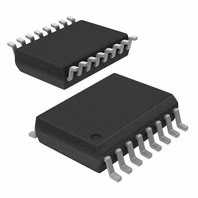
| 描述 | IC ADC 16BIT 250KSPS SRL 20-SOIC模数转换器 - ADC 16-Bit 250kHz CMOS w/Serial Interface |
| 产品分类 | |
| 品牌 | Texas Instruments |
| 产品手册 | http://www.ti.com/litv/slas324c |
| 产品图片 |
|
| rohs | 符合RoHS无铅 / 符合限制有害物质指令(RoHS)规范要求 |
| 产品系列 | 数据转换器IC,模数转换器 - ADC,Texas Instruments ADS8509IBDW- |
| 数据手册 | |
| 产品型号 | ADS8509IBDW |
| 产品培训模块 | http://www.digikey.cn/PTM/IndividualPTM.page?site=cn&lang=zhs&ptm=13240 |
| 产品目录页面 | |
| 产品种类 | 模数转换器 - ADC |
| 位数 | 16 |
| 供应商器件封装 | 20-SOIC |
| 信噪比 | 88 dB |
| 其它名称 | 296-18085-5 |
| 分辨率 | 16 bit |
| 制造商产品页 | http://www.ti.com/general/docs/suppproductinfo.tsp?distId=10&orderablePartNumber=ADS8509IBDW |
| 包装 | 管件 |
| 单位重量 | 537.300 mg |
| 商标 | Texas Instruments |
| 安装类型 | 表面贴装 |
| 安装风格 | SMD/SMT |
| 封装 | Tube |
| 封装/外壳 | 20-SOIC(0.295",7.50mm 宽) |
| 封装/箱体 | SOIC-20 |
| 工作温度 | -40°C ~ 85°C |
| 工作电源电压 | 5 V |
| 工厂包装数量 | 25 |
| 接口类型 | Serial, SPI |
| 数据接口 | SPI |
| 最大功率耗散 | 100 mW |
| 最大工作温度 | + 85 C |
| 最小工作温度 | - 40 C |
| 标准包装 | 25 |
| 特性 | - |
| 电压参考 | Internal, External |
| 电压源 | 模拟和数字 |
| 系列 | ADS8509 |
| 结构 | SAR |
| 转换器数 | 1 |
| 转换器数量 | 1 |
| 转换速率 | 250 kS/s |
| 输入数和类型 | 3 个单端,单极3 个单端,双极 |
| 输入类型 | Single-Ended |
| 通道数量 | 1 Channel |
| 配用 | /product-detail/zh/ADS8509EVM/296-20818-ND/1216423 |
| 采样率(每秒) | 250k |


- 商务部:美国ITC正式对集成电路等产品启动337调查
- 曝三星4nm工艺存在良率问题 高通将骁龙8 Gen1或转产台积电
- 太阳诱电将投资9.5亿元在常州建新厂生产MLCC 预计2023年完工
- 英特尔发布欧洲新工厂建设计划 深化IDM 2.0 战略
- 台积电先进制程称霸业界 有大客户加持明年业绩稳了
- 达到5530亿美元!SIA预计今年全球半导体销售额将创下新高
- 英特尔拟将自动驾驶子公司Mobileye上市 估值或超500亿美元
- 三星加码芯片和SET,合并消费电子和移动部门,撤换高东真等 CEO
- 三星电子宣布重大人事变动 还合并消费电子和移动部门
- 海关总署:前11个月进口集成电路产品价值2.52万亿元 增长14.8%


PDF Datasheet 数据手册内容提取
ADS8509 www.ti.com SLAS324C–OCTOBER2004–REVISEDAPRIL2010 16-BIT 250-KSPS SERIAL CMOS SAMPLING ANALOG-TO-DIGITAL CONVERTER CheckforSamples:ADS8509 FEATURES DESCRIPTION 1 • 250-kHzSamplingRate The ADS8509 is a complete 16-bit sampling 2 • 4-V,5-V,10-V,±3.33-V, ±5-V,and±10-VInput analog-to-digital (A/D) converter using state-of-the-art Ranges CMOS structures. It contains a complete 16-bit, capacitor-based, successive approximation register • ±2LSBMaxINL (SAR) A/D converter with sample-and-hold, • ±1LSBMaxDNL,16-BitNoMissingCodes reference, clock, and a serial data interface. Data can • SPICompatibleSerialOutputwithDaisy-Chain be output using the internal clock or can be (TAG)Feature synchronizedtoanexternaldataclock.TheADS8509 also provides an output synchronization pulse for • Single5-VSupply easeofusewithstandardDSPprocessors. • Pin-CompatiblewithADS7809(LowSpeed) The ADS8509 is specified at a 250-kHz sampling rate and12-BitADS8508/7808 over the full temperature range. Precision resistors • UsesInternalorExternalReference provide various input ranges including ±10 V and 0 V • 70-mWTypPowerDissipationat250KSPS to 5 V, while the innovative design allows operation • 20-PinSOand28-PinSSOPPackages from a single +5-V supply with power dissipation under100mW. • SimpleDSPInterface The ADS8509 is available in 20-pin SO and 28-pin APPLICATIONS SSOP packages, both fully specified for operation overtheindustrial-40°Cto85°Ctemperaturerange. • IndustrialProcessControl • DataAcquisitionSystems • DigitalSignalProcessing • MedicalEquipment • Instrumentation Successive Approximation Register Clock EXT/INT 9.8 kW CDAC R1IN 4.9 kW BUSY R2IN Serial DATACLK 2.5 kW Data R3IN 10 kW Out DATA Comparator & R/C Control CAP SB/BTC Buffer Internal CS +2.5 V Ref PWRD 4 kW REF 1 Pleasebeawarethatanimportantnoticeconcerningavailability,standardwarranty,anduseincriticalapplicationsofTexas Instrumentssemiconductorproductsanddisclaimerstheretoappearsattheendofthisdatasheet. Alltrademarksarethepropertyoftheirrespectiveowners. 2 PRODUCTIONDATAinformationiscurrentasofpublicationdate. Copyright©2004–2010,TexasInstrumentsIncorporated Products conform to specifications per the terms of the Texas Instruments standard warranty. Production processing does not necessarilyincludetestingofallparameters.
ADS8509 SLAS324C–OCTOBER2004–REVISEDAPRIL2010 www.ti.com This integrated circuit can be damaged by ESD. Texas Instruments recommends that all integrated circuits be handled with appropriateprecautions.Failuretoobserveproperhandlingandinstallationprocedurescancausedamage. ESDdamagecanrangefromsubtleperformancedegradationtocompletedevicefailure.Precisionintegratedcircuitsmaybemore susceptibletodamagebecauseverysmallparametricchangescouldcausethedevicenottomeetitspublishedspecifications. PACKAGE/ORDERINGINFORMATION(1) MINIMUM NO MINIMUM SPECIFICATION RELATIVE PACKAGE PACKAGE ORDERING TRANSPORT PRODUCT MISSING SINAD TEMPERATURE ACCURACY LEAD DESIGNATOR NUMBER MEDIA,QTY CODE (dB) RANGE (LSB) ADS8509IBDW Tube,25 SO-20 DW ADS8509IBDWR TapeandReel,2000 ADS8509IB ±2 16 85 –40°Cto85°C ADS8509IBDB Tube,50 SSOP-28 DB ADS8509IBDBR TapeandReel,2000 ADS8509IDW Tube,25 SO-20 DW ADS8509IDWR TapeandReel,2000 ADS8509I ±3 15 83 –40°Cto85°C ADS8509IDB Tube,50 SSOP-28 DB ADS8509IDBR TapeandReel,2000 (1) Forthemostcurrentpackageandorderinginformation,seethePackageOptionAddendumattheendofthisdocument,orvisitthe deviceproductfolderonwww.ti.com. ABSOLUTE MAXIMUM RATINGS overoperatingfree-airtemperaturerange(unlessotherwisenoted)(1) UNIT R1 ±25V IN R2 ±25V IN Analoginputs R3 ±25V IN REF +V +0.3VtoAGND2–0.3V ANA CAP IndefiniteshorttoAGND2,momentaryshorttoV ANA DGND,AGND2 ±0.3V V 6V ANA Groundvoltagedifferences V toV 0.3V DIG ANA V 6V DIG Digitalinputs –0.3Vto+V +0.3V DIG Maximumjunctiontemperature 165°C Storagetemperaturerange –65°Cto150°C Internalpowerdissipation 700mW Leadtemperature(soldering,1.6mmfromcase10seconds) 260°C (1) Allvoltagevaluesarewithrespecttonetworkgroundterminal. 2 Copyright©2004–2010,TexasInstrumentsIncorporated ProductFolderLink(s):ADS8509
ADS8509 www.ti.com SLAS324C–OCTOBER2004–REVISEDAPRIL2010 ELECTRICAL CHARACTERISTICS AtT =–40°Cto85°C,f =250kHz,V =V =5V,usinginternalreferenceand0.1%,0.25-Wfixedresistors(see A s DIG ANA Figure29andFigure30)(unlessotherwisespecified) ADS8509I ADS8509IB PARAMETER TESTCONDITIONS UNIT MIN TYP MAX MIN TYP MAX Resolution 16 16 Bits ANALOGINPUT Voltagerange(1) Impedance(1) Capacitance 50 50 pF THROUGHPUTSPEED Conversioncycle Acquireandconvert 4 4 ms Throughputrate 250 250 kHz DCACCURACY INL Integrallinearityerror –3 3 –2 2 LSB(2) DNL Differentiallinearityerror –2 2 –1 1 LSB Nomissingcodes 15 16 Bits Transitionnoise(3) 1 1 LSB Full-scale ±10-VRange Int.ref.with0.1%externalfixed –0.5 0.5 –0.5 0.5 error(4)(5) Allotherranges resistors –0.5 0.5 –0.5 0.5 %FSR Full-scaleerrordrift Int.ref. ±7 ±7 ppm/°C Full-scale ±10-VRange Ext.ref.with0.1%external –0.5 0.5 –0.5 0.5 error(4)(5) Allotherranges fixedresistors –0.5 0.5 –0.5 0.5 %FSR Full-scaleerrordrift Ext.ref. ±2 ±2 ppm/°C Bipolarzeroerror(4) –10 10 –5 5 mV Bipolarzeroerrordrift ±0.4 ±0.4 ppm/°C 10-VRange –5 5 –5 5 Unipolarzero error(4) 4-Vand5-V –3 3 –3 3 mV Range Unipolarzeroerrordrift ±2 ±2 ppm/°C Recoverytoratedaccuracyafter 1-mFCapacitortoCAP 1 1 ms powerdown Powersupplysensitivity –8 8 –8 8 (VDIG=VANA=VD) +4.75V<VD<+5.25V LSB ACACCURACY SFDR Spurious-freedynamicrange fI=20kHz 90 99 95 99 dB(6) THD Totalharmonicdistortion fI=20kHz –98 –90 –98 –93 dB SINAD fI=20kHz 83 88 85 88 dB Signal-to-(noise+distortion) –60-dBInput 30 32 dB SNR Signal-to-noiseratio fI=20kHz 83 88 86 88 dB Full-powerbandwidth(7) 500 500 kHz SAMPLINGDYNAMICS Aperturedelay 5 5 ns Transientresponse FSStep 2 2 ms Overvoltagerecovery(8) 150 150 ns (1) ±10V,0Vto5V,etc.(seeTable2).Fornormaloperation,theanaloginputshouldnotexceedconfiguredrange±20%. (2) LSBmeansleastsignificantbit.Forthe±10-Vinputrange,oneLSBis305mV. (3) Typicalrmsnoiseatworstcasetransitionsandtemperatures. (4) AsmeasuredwithfixedresistorsshowninFigure29andFigure30.Adjustabletozerowithexternalpotentiometer.Factorycalibrated with0.1%,0.25-Wresistors. (5) Forbipolarinputranges,full-scaleerroristheworstcaseof–full-scaleor+full-scaleuncalibrateddeviationfromidealfirstandlastcode transitions,dividedbythetransitionvoltage(notdividedbythefull-scalerange)andincludestheeffectofoffseterror.Forunipolarinput ranges,full-scaleerroristhedeviationofthelastcodetransitiondividedbythetransitionvoltage.Italsoincludestheeffectofoffset error. (6) AllspecificationsindBarereferredtoafull-scale±10-Vinput. (7) Full-powerbandwidthisdefinedasthefull-scaleinputfrequencyatwhichsignal-to-(noise+distortion)degradesto60dB. (8) Recoverstospecifiedperformanceafter2xFSinputovervoltage. Copyright©2004–2010,TexasInstrumentsIncorporated 3 ProductFolderLink(s):ADS8509
ADS8509 SLAS324C–OCTOBER2004–REVISEDAPRIL2010 www.ti.com ELECTRICAL CHARACTERISTICS (continued) AtT =–40°Cto85°C,f =250kHz,V =V =5V,usinginternalreferenceand0.1%,0.25-Wfixedresistors(see A s DIG ANA Figure29andFigure30)(unlessotherwisespecified) ADS8509I ADS8509IB PARAMETER TESTCONDITIONS UNIT MIN TYP MAX MIN TYP MAX REFERENCE Internalreferencevoltage Noload 2.48 2.5 2.52 2.48 2.5 2.52 V Internalreferencesourcecurrent 1 1 mA (mustuseexternalbuffer) Internalreferencedrift 8 8 ppm/°C Externalreferencevoltagerange 2.3 2.5 2.7 2.3 2.5 2.7 V forspecifiedlinearity Externalreferencecurrentdrain Ext.2.5-Vref. 100 100 mA DIGITALINPUTS Logiclevels VIL Low-levelinputvoltage –0.3 0.8 –0.3 0.8 V VIH High-levelinputvoltage 2.0 VDIG+0.3V 2.0 VDIG+0.3V V IIL Low-levelinputcurrent VIL=0V ±10 ±10 mA IIH High-levelinputcurrent VIH=5V ±10 ±10 mA DIGITALOUTPUTS Dataformat(serial16-bits) Datacoding(binary2's complementorstraightbinary) Pipelinedelay(conversionresults onlyavailableaftercompleted conversion) Dataclock(selectableforinternal orexternaldataclock) Internalclock(outputonlywhen EXT/INTLow 9 9 MHz transmittingdata) Externalclock(canrun EXT/INTHigh 0.1 26 0.1 26 continuallybutnotrecommended MHz foroptimumperformance) VOL Low-leveloutputvoltage ISINK=1.6mA 0.4 0.4 V VOH High-leveloutputvoltage ISOURCE=500mA 4 4 V Hi-ZState, ±5 ±5 mA Leakagecurrent VOUT=0VtoVDIG Outputcapacitance Hi-ZState 15 15 pF POWERSUPPLIES VDIG Digitalinputvoltage 4.75 5 5.25 4.75 5 5.25 V VANA Analoginputvoltage 4.75 5 5.25 4.75 5 5.25 V Mustbe≤VANA IDIG Digitalinputcurrent 4 4 mA IANA Analoginputcurrent 10 10 mA POWERDISSIPATION PWRDLow fS=250kHz 70 100 70 100 mW PWRDHigh 50 50 mW TEMPERATURERANGE Specifiedperformance –40 85 –40 85 °C Deratedperformance(9) –55 125 –55 125 °C Storage –65 150 –65 150 °C THERMALRESISTANCE(qJA) SSOP 62 62 °C/W SO 46 46 °C/W (9) Theinternalreferencemaynotbestartedcorrectlybeyondtheindustrialtemperaturerange(–40°Cto85°C),thereforeuseofan externalreferenceisrecommended. 4 Copyright©2004–2010,TexasInstrumentsIncorporated ProductFolderLink(s):ADS8509
ADS8509 www.ti.com SLAS324C–OCTOBER2004–REVISEDAPRIL2010 PIN CONFIGURATIONS DWPACKAGE SO-20 (TOPVIEW) R1IN 1 20 VDIG AGND1 2 19 VANA R2IN 3 18 PWRD R3IN 4 17 BUSY CAP 5 16 CS REF 6 15 R/C AGND2 7 14 TAG SB/BTC 8 13 DATA EXT/INT 9 12 DATACLK DGND 10 11 SYNC DBPACKAGE SSOP-28 (TOPVIEW) R1IN 1 28 VDIG AGND1 2 27 VANA R2IN 3 26 PWRD R3IN 4 25 BUSY NC 5 24 CS CAP 6 23 NC REF 7 22 NC NC 8 21 R/C AGND2 9 20 NC NC 10 19 TAG NC 11 18 NC SB/BTC 12 17 DATA EXT/INT 13 16 DATACLK DGND 14 15 SYNC Copyright©2004–2010,TexasInstrumentsIncorporated 5 ProductFolderLink(s):ADS8509
ADS8509 SLAS324C–OCTOBER2004–REVISEDAPRIL2010 www.ti.com TerminalFunctions TERMINAL DESCRIPTION NAME DBNO. DWNO. I/O AGND1 2 2 – Analogground.Usedinternallyasgroundreferencepoint.Minimalcurrentflow. AGND2 9 7 – Analogground BUSY 25 17 O Busyoutput.Fallswhenaconversionisstartedandremainslowuntiltheconversioniscompleted andthedataislatchedintotheoutputshiftregister. CAP 6 5 – Referencebuffercapacitor.2.2-mFTantalumtoground. CS 24 16 – Chipselect.InternallyORedwithR/C. DATA 17 13 O Serialdataoutput.DataissynchronizedtoDATACLKwiththeformatdeterminedbythelevelof SB/BTC.Intheexternalclockmode,after16bitsofdata,theADS8509outputsthelevelinputon TAGaslongasCSislowandR/Cishigh(seeFigure8andFigure9).IfEXT/INTislow,datais validonboththerisingandfallingedgesofDATACLK,andbetweenconversionsDATAstaysat theleveloftheTAGinputwhentheconversionwasstarted. DATACLK 16 12 I/O EitheraninputoranoutputdependingontheEXT/INTlevel.Outputdataissynchronizedtothis clock.IfEXT/INTislow,DATACLKtransmits16pulsesaftereachconversionandthenremains lowbetweenconversions. DGND 14 10 – Digitalground EXT/INT 13 9 – Selectsexternalorinternalclockfortransmittingdata.Ifhigh,dataisoutputsynchronizedtothe clockinputonDATACLK.Iflow,aconvertcommandinitiatesthetransmissionofthedatafromthe previousconversion,alongwith16-clockpulsesoutputonDATACLK. NC 5,8,10, – – Noconnect 11,18, 20,22, 23 PWRD 26 18 I Powerdowninput.Ifhigh,conversionsareinhibitedandpowerconsumptionissignificantly reduced.Resultsfromthepreviousconversionaremaintainedintheoutputshiftregister. R/C 21 15 I Read/convertinput.WithCSlow,afallingedgeonR/Cputstheinternalsample-and-holdintothe holdstateandstartsaconversion.WhenEXT/INTislow,thisalsoinitiatesthetransmissionofthe dataresultsfromthepreviousconversion.IfEXT/INTishigh,arisingedgeonR/CwithCSlowor afallingedgeonCSwithR/ChightransmitsapulseonSYNCandinitiatesthetransmissionof datafromthepreviousconversion. REF 7 6 I/O Referenceinput/output.Outputsinternal2.5-Vreference.Canalsobedrivenbyexternalsystem reference.Inbothcases,bypasstogroundwitha2.2-mFtantalumcapacitor. R1 1 1 I Analoginput.SeeTable2forinputrangeconnections. IN R2 3 3 I Analoginput.SeeTable2forinputrangeconnections. IN R3 4 4 I Analoginput.SeeTable2forinputrangeconnections. IN SB/BTC 12 8 I Selectstraightbinaryorbinary2'scomplementdataoutputformat.Ifhigh,dataisoutputina straightbinaryformat.Iflow,dataisoutputinabinary2'scomplementformat. SYNC 15 11 O Syncoutput.ThispinisusedtosupplyadatasynchronizationpulsewhentheEXTlevelishigh andatleastoneexternalclockpulsehasoccurredwhennotinthereadmode.Seetheexternal clockmodesdesciptions. TAG 19 14 I Taginputforuseintheexternalclockmode.IfEXTishigh,digitaldatainputfromTAGisoutput onDATAwithadelaythatisdependentontheexternalclockmode.SeeFigure8andFigure9. V 27 19 I Analogsupplyinput.Nominally+5V.Connectdirectlytopin20anddecoupletogroundwith ANA 0.1-mFceramicand10-mFtantalumcapacitors. V 28 20 I Digitalsupplyinput.Nominally+5V.Connectdirectlytopin19.Mustbe≤V . DIG ANA 6 Copyright©2004–2010,TexasInstrumentsIncorporated ProductFolderLink(s):ADS8509
ADS8509 www.ti.com SLAS324C–OCTOBER2004–REVISEDAPRIL2010 TIMING REQUIREMENTS, T = –40°C to 85°C A PARAMETER MIN TYP MAX UNIT t Pulseduration,convert 40 ns w1 t Delaytime,BUSYfromR/Clow 6 20 ns d1 t Pulseduration,BUSYlow 2.2 ms w2 t Delaytime,BUSY,afterendofconversion 5 ns d2 t Delaytime,aperture 5 ns d3 t Conversiontime 2.2 ms conv t Acquisitiontime 1.8 ms acq t +t Cycletime 4 ms conv acq t Delaytime,R/ClowtointernalDATACLKoutput 270 ns d4 t Cycletime,internalDATACLK 110 ns c1 t Delaytime,datavalidtointernalDATACLKhigh 15 35 ns d5 t Delaytime,datavalidafterinternalDATACLKlow 20 35 ns d6 t Cycletime,externalDATACLK 35 ns c2 t Pulseduration,externalDATACLKhigh 15 ns w3 t Pulseduration,externalDATACLKlow 15 ns w4 t Setuptime,R/Crise/falltoexternalDATACLKhigh 15 ns su1 t Setuptime,R/CtransitiontoCStransition 10 ns su2 t Delaytime,SYNC,afterexternalDATACLKhigh 3 35 ns d7 t Delaytime,datavalid 2 20 ns d8 t Delaytime,CStorisingedge 10 ns d9 t Delaytime,previousdataavailableafterCS,R/Clow 2 ms d10 t Setuptime,BUSYtransitiontofirstexternalDATACLK 5 ns su3 t Delaytime,finalexternalDATACLKtoBUSYfallingedge 1 ms d11 t Setuptime,TAGvalid 0 ns su3 t Holdtime,TAGvalid 2 ns h1 PARAMETER MEASUREMENT INFORMATION CS R/C R/C CS tsu1 tsu1 tsu1 tsu1 External External DATACLK DATACLK CS Set Low, Discontinuous Ext DATACLK R/C Set Low, Discontinuous Ext DATACLK CS BUSY tsu2 tsu2 tsu3 1 2 External R/C DATACLK CS Set Low, Discontinuous Ext DATACLK Figure1. CriticalTiming Copyright©2004–2010,TexasInstrumentsIncorporated 7 ProductFolderLink(s):ADS8509
ADS8509 SLAS324C–OCTOBER2004–REVISEDAPRIL2010 www.ti.com PARAMETER MEASUREMENT INFORMATION (continued) tw1 tw1 R/C td1 tw2 td1 tw2 BUSY td3 td2 td3 td2 td11 td11 STATUS Nth Conversion ECrorrorrection (N+1)th Accquisition (N+1)th Conversion ECrorrorrection (N+2)th Accquisition tconv tacq tconv tacq td4 tc1 td4 Internal DATACLK 1 2 16 1 2 16 td6 td5 DATA TAG = 0 D15 D0 TAG = 0 D15 D0 TAG = 0 (N−1)th Conversion Data Nth Conversion Data CS, EXT/INT, and TAG are tied low 8starts READ Figure2. BasicConversionTiming(InternalDATACLK-ReadPreviousDataDuringConversion) tw1 tw1 R/C td1 tw2 td1 tw2 BUSY td2 td2 td3 td11 td3 td11 STATUS Nth Conversion Error (N+1)th Accquisition (N+1)th ConversionError (N+2)th Accquisition Correction Correction tconv tacq tconv tacq tsu1 tsu3 tsu1 tsu3 External DATACLK 1 16 1 2 16 1 16 1 2 16 No more No more DATA TAG = 0 dshaitfat otout TAG = 0 Nth Data TAG = 0 dshaitfat otout TAG = 0 (N+1)th Data TAG = 0 EXT/INT tied high, CS and TAG are tied low tw1 + tsu1 starts READ Figure3. BasicConversionTiming(ExternalDATACLK) 8 Copyright©2004–2010,TexasInstrumentsIncorporated ProductFolderLink(s):ADS8509
ADS8509 www.ti.com SLAS324C–OCTOBER2004–REVISEDAPRIL2010 PARAMETER MEASUREMENT INFORMATION (continued) tw1 R/C td1 tw2 tsu1 td1 BUSY td2 td3 td11 td3 STATUS Nth Conversion Error (N+1)th Accquisition Correction tconv tsu3 tacq External tw3tc2 tw4 tsu1 DATACLK 0 1 2 3 4 5 10 11 12 13 14 15 16 SYNC = 0 td8 Nth Conversion Data td8 DATA D15 D14 D13 D12 D11 D10 D05 D04 D03 D02 D01 D00 Null T00 Txx tsu3 th1 TAG T00 T01 T02 T03 T04 T05 T06 T11 T12 T13 T14 T15 T16 Null T17 Tyy EXT/INT tied high, CS tied low tw1 + tsu1 starts READ Figure4. ReadAfterConversion(DiscontinuousExternalDATACLK) tw1 R/C td1 tw2 BUSY td3 td10 td2 Error STATUS Nth Conversion Correction tsu3 tconv tc2 tsu1 tw3 tw4 td11 External DATACLK 0 1 2 3 4 5 10 11 12 13 14 15 16 SYNC = 0 td8 Nth Conversion Data td8 DATA D15 D14 D13 D12 D11 D10 D05 D04 D03 D02 D01 D00 EXT/INT tied high, CS and TAG tied low Rising DATACLK change DATA, tw1 + tsu1 Starts READ TAG is not recommended for this mode. There is not enough time to do so without violating td11. Figure5. ReadDuringConversion(DiscontinuousExternalDATACLK) Copyright©2004–2010,TexasInstrumentsIncorporated 9 ProductFolderLink(s):ADS8509
ADS8509 SLAS324C–OCTOBER2004–REVISEDAPRIL2010 www.ti.com PARAMETER MEASUREMENT INFORMATION (continued) tw1 R/C td1 tsu1 tsu1 td1 tw2 BUSY td2 td3 td11 td3 Error STATUS Nth ConversionCorrection (N+1)th Accquisition tconv tacq tsu1 tsu3 tw3 tc2 tw4 tsu1 External DATACLK 0 1 2 3 4 5 6 7 12 13 14 15 16 17 18 tc2 td7 SYNC=0 td8 Nth Conversion Data td8 DATA D15 D14 D13 D12 D11 D10 D05 D04 D03 D02 D01 D00 Null T00 Txx tsu3 th1 TAG T00 T01 T02 T03 T04 T05 T06 T11 T12 T13 T14 T15 T16 T17 Tyy EXT/INT tied high, CS tied low tw1 + tsu1 starts READ Figure6. ReadAfterConversionWithSYNC(DiscontinuousExternalDATACLK) tw1 R/C td1 tw2 BUSY td3 td10 td2 Error STATUS Nth Conversion Correction tsu3 tconv Externtsaul1 tsu1 tsu1 tw3 ttcw24 td11 DATACLK 0 1 2 3 4 5 6 7 12 13 14 15 16 17 18 td7 tc2 SYNC = 0 td8 Nth Conversion Data td8 DATA D15 D14 D13 D12 D11 D10 D05 D04 D03 D02 D01 D00 tw1 + tsu1 Starts READ EXT/INT tied high, CS and TAG tied low TAG is not recommended for this mode. There is not enough time to do so without violating td11. Figure7. ReadDuringConversionWithSYNC(DiscontinuousExternalDATACLK) 10 Copyright©2004–2010,TexasInstrumentsIncorporated ProductFolderLink(s):ADS8509
ADS8509 www.ti.com SLAS324C–OCTOBER2004–REVISEDAPRIL2010 PARAMETER MEASUREMENT INFORMATION (continued) 9 1 g Ta 1 8 Tag Tag 1 9 d t 0 7 Tag Tag 1 8 B) 1 S 6 L 1 Bit 0 ( Tag 7 1 Bit 1 Tag 15 4 4 2 Bit 1 Tag B) 3 S M 1 td8 Bit 15 ( Tag 2 0 g 2 Ta c 4 t w t 1 c2 d7 t 0 su1 su2 t t t 3 w t 1 d 2 t u s t 1 w t alK S C Y C A G xternTACL C R/ BUS SYN DAT TA EA D Figure8. ConversionandReadTimingwithContinuousExternalDATACLK(EXT/INTTiedHigh)Read AfterConversions(NotRecommended) Copyright©2004–2010,TexasInstrumentsIncorporated 11 ProductFolderLink(s):ADS8509
ADS8509 SLAS324C–OCTOBER2004–REVISEDAPRIL2010 www.ti.com PARAMETER MEASUREMENT INFORMATION (continued) 9 1 g Ta 8 Tag 1 Tag 1 8 d 7 t g 0 g 1 Ta Ta Bit 0 (LSB) Tag 16 B) td10 8 15 (MS Tag 1 td Bit 2 c t 0 1 g su Ta t 1 u s w4 t t 1 w t 2 c t 3 1 w d t 2 t u s t alK S C Y C A G xternTACL C R/ BUS SYN DAT TA EA D Figure9. ConversionandReadTimingwithContinousExternalDATACLK(EXT/INTTiedHigh)Read PreviousConversionResultsDuringConversion(NotRecommended) 12 Copyright©2004–2010,TexasInstrumentsIncorporated ProductFolderLink(s):ADS8509
ADS8509 www.ti.com SLAS324C–OCTOBER2004–REVISEDAPRIL2010 TYPICAL CHARACTERISTICS SPURIOUSFREEDYNAMICRANGE TOTALHARMONICDISTORTION vs vs FREE-AIRTEMPERATURE FREE-AIRTEMPERATURE B 105 −100 d e − dB ang 100 n − −95 R o namic 95 Distorti −90 us Free Dy 8950 Harmonic −−8805 urio otal p T R − S 80 ffsi == 2205 0kH KzSPS, HD − −75 ffsi == 2205 0kH KzSPS, D T SF 75 −70 −40 25 85 −40 25 85 TA − Free-Air Temperature − (cid:1)C TA − Free-Air Temperature − (cid:1)C Figure10. Figure11. SIGNAL-TO-NOISERATIO SIGNAL-TO-NOISEANDDISTORTION vs vs FREE-AIRTEMPERATURE FREE-AIRTEMPERATURE 100 B 100 atio − dB 9905 ffsi == 2205 0kH KzSPS, Distortion − d 9905 ffsi == 2205 0kH KzSPS, e R nd s a Noi 85 se 85 Signal-to- 80 nal-To-Noi 80 NR − 75 − Sig 75 S D A 70 SIN 70 −40 25 85 −40 25 85 TA − Free-Air Temperature − (cid:1)C TA − Free-Air Temperature − (cid:1)C Figure12. Figure13. SIGNAL-TO-NOISERATIO SIGNAL-TO-NOISEANDDISTORTION vs vs INPUTFREQUENCY INPUTFREQUENCY 90 B 90 d − B on atio − d 85 Distorti 85 e R 80 nd 80 s a oi e Signal-to-N 75 nal-To-Nois 75 NR − 70 − Sig 70 S D A 65 SIN 65 1 10 100 1 10 100 fi − Input Frequency − kHz fi − Input Frequency − kHz Figure14. Figure15. Copyright©2004–2010,TexasInstrumentsIncorporated 13 ProductFolderLink(s):ADS8509
ADS8509 SLAS324C–OCTOBER2004–REVISEDAPRIL2010 www.ti.com TYPICAL CHARACTERISTICS (continued) SPURIOUSFREEDYNAMICRANGE TOTALHARMONICDISTORTION vs vs INPUTFREQUENCY INPUTFREQUENCY B 105 −105 d − B Spurious Free Dynamic Range 10889900505 − Total Harmonic Distortion − d −−−−−10889900505 R − 75 HD −75 D T SF 70 −70 1 10 100 1 10 100 fi − Input Frequency − kHz fi − Input Frequency − kHz Figure16. Figure17. INTERNALREFERENCEVOLTAGE BIPOLARZEROSCALEERROR vs vs FREE-AIRTEMPERATURE FREE-AIRTEMPERATURE 2.510 5 2.508 4 External Reference, V V ±10-V Range − 2.506 m 3 Internal Reference Voltage 222222......444555999000468024 Bipolar Zero Scale Error − −−−012321 2.492 −4 2.490 −5 −55 −35 −15 5 25 45 65 85 105 −40 −25 −10 5 20 35 50 65 80 TA − Free-Air Temperature − (cid:1)C TA − Free-Air Temperature − (cid:1)C Figure18. Figure19. FULLSCALEERROR SUPPLYCURRENT vs vs FREE-AIRTEMPERATURE FREE-AIRTEMPERATURE 0.20 20 External Reference, 0.15 ±10 V Range 19 for 5 Representative 18 SR 0.10 Parts %F A 17 e Error − 0.050 urrent − m 1156 Full Scal−−00..1005 Supply C 1134 12 −0.15 11 −0.20 10 −40 −25 −10 5 20 35 50 65 80 −40 −25 −10 5 20 35 50 65 80 TA − Free-Air Temperature − (cid:1)C TA − Free-Air Temperature − (cid:1)C Figure20. Figure21. 14 Copyright©2004–2010,TexasInstrumentsIncorporated ProductFolderLink(s):ADS8509
ADS8509 www.ti.com SLAS324C–OCTOBER2004–REVISEDAPRIL2010 TYPICAL CHARACTERISTICS (continued) PERFORMANCE vs HISTOGRAM CAPPINCAPACITORESR 4500 100 44222244 8192 4000 Conversions 95 |THD| of a DC Input 3500 90 3000 ce 85 SINAD an 80 2500 m Hits 2000 2082 erfor 75 1484 P 70 1500 65 1000 60 2.2 m F Capacitor on 500 4 149 238 11 55 CAP Pin (pin 6) 0 50 −3 −2 −1 0 1 2 3 0 1 2 3 4 5 6 7 8 9 10 11 Code ESR − Resistance − (cid:1) Figure22. Figure23. INTEGRALNONLINEARITY 2.5 2 fs = 250 KSPS 1.5 1 s 0.5 B S − L 0 NL −0.5 I −1 −1.5 −2 −2.5 0 16384 32768 49152 65536 Code Figure24. DIFFERENTIALNONLINEARITY 2.5 fs = 250 KSPS 2 1.5 1 s SB 0.5 L L − 0 DN −0.5 −1 −1.5 −2 −2.5 0 16384 32768 49152 65536 Code Figure25. Copyright©2004–2010,TexasInstrumentsIncorporated 15 ProductFolderLink(s):ADS8509
ADS8509 SLAS324C–OCTOBER2004–REVISEDAPRIL2010 www.ti.com TYPICAL CHARACTERISTICS (continued) FFT(20-kHzInput) 20 8192 Points, 0 fs = 250 KSPS, −20 fi = 20 kHz, 0 dB SINAD = 86.0 dB, −40 THD = −98.7 dB B d −60 − de −80 u plit −100 m A −120 −140 −160 −180 0 25 50 75 100 125 f − Frequency − kHz Figure26. BASIC OPERATION TwosignalscontrolconversionintheADS8509:CSandR/C.ThesetwosignalsareinternallyORedtogether.To start a conversion the chip must be selected, CS low, and the conversion signal must be active, R/C low. Either signal can be brought low first. Conversion starts on the falling edge of the second signal. BUSY goes low when conversion starts and returns high after the data from that conversion is shifted into the internal storage register. SamplingbeginswhenBUSYgoeshigh. To reduce the number of control pins CS can be tied low permanently. The R/C pin now controls conversion and data reading exclusively. In the external clock mode this means that the ADS8509 clocks out data whenever R/C isbroughthighandtheexternalclockisactive.Intheinternalclockmodedataisclockedouteveryconvertcycle regardless of the states of CS and R/C. The ADS8509 provides a TAG input for cascading multiple converters together. READING DATA The conversion result is available as soon as BUSY returns to high, therefore data always represents the conversion previously completed even when it is read during a conversion. The ADS8509 outputs serial data in either straight binary or binary two’s compliment format. The SB/BTC pin controls the format. Data is shifted out MSBfirst.Thefirstconversionimmediatelyfollowingapower-updoesnotproduceavalidconversionresult. Data can be clocked out with either the internally generated clock or with an external clock. The EXT/INT pin controls this function. If an external clock is used, the TAG input can be used to daisy-chain multiple ADS8509 datapinstogether. INTERNAL DATACLK In internal clock mode data for the previous conversion is clocked out during each conversion period. The internal data clock is synchronized to the internal conversion clock so that is does not interfere with the conversionprocess. The DATACLK pin becomes an output when EXT/INT is low. 16 Clock pulses are generated at the beginning of eachconversionaftertimingt issatisfied,i.e.onlythepreviousconversionresultcanbereadduringconversion. 8 DATACLK returns to low when it is inactive. The 16 bits of serial data are shifted out the DATA pin synchronous to this clock with each bit available on a rising and then a falling edge. The DATA pin returns to the state of the TAGpininputsensedatthestartoftransmission. EXTERNAL DATACLK The external clock mode offers several ways to retrieve conversion results. However, since the external clock cannotbesynchronizedtotheinternalconversionclockcaremustbetakentoavoidcorruptingthedata. 16 Copyright©2004–2010,TexasInstrumentsIncorporated ProductFolderLink(s):ADS8509
ADS8509 www.ti.com SLAS324C–OCTOBER2004–REVISEDAPRIL2010 When EXT/INT is set high, the R/C and CS signals control the read state. When the read state is initiated, the result from the previously completed conversion is shifted out the DATA pin synchronous to the external clock that is connected to the DATACLK pin. Each bit is available on a falling and then a rising edge. The maximum external clock speed of 28.5 MHz allows data to be shifted out quickly either at the beginning of conversion or thebeginningofsampling. There are several modes of operation available when using an external clock. It is recommended that the external clock run only while reading data. This is discontinuous clock mode. Since the external clock is not synchronized to the internal clock that controls conversion slight changes in the external clock can cause conflicts that can corrupt the conversion process. Specifications with a continuously running external clock cannot be ensured. It is especially important that the external clock does not run during the second half of the conversioncycle(approximatelythetimeperiodspecifiedbyt ,seetheTIMINGREQUIREMENTStable). d11 In discontinuous clock mode data can be read during conversion or during sampling, with or without a SYNC pulse. Data read during conversion must meet the t timing specification. Data read during sampling must be d11 completebeforestartingaconversion. Whether reading during sampling or during conversion a SYNC pulse is generated whenever at least one rising edge of the external clock occurs while the part is not in the read state. In the discontinuous external clock with SYNC mode a SYNC pulse follows the first rising edge after the read command. The data is shifted out after the SYNC pulse. The first rising clock edge after the read command generates a SYNC pulse. The SYNC pulse can bedetectedonthenextfallingedgeandthenthenextrisingedge.Successively,eachbitcanbereadfirstonthe falling edge and then on the next rising edge. Thus 17 clock pulses after the read command are required to read onthefallingedge.18Clockpulsesarenecessarytoreadontherisingedge. Table1.DATACLKPulses DATACLKPULSESREQUIRED DESCRIPTION WITHSYNC WITHOUTSYNC ReadonfallingedgeofDATACLK 17 16 ReadonrisingedgeofDATACLK 18 17 If the clock is entirely inactive when not in the read state a SYNC pulse is not generated. In this case the first rising clock edge shifts out the MSB. The MSB can be read on the first falling edge or on the next rising edge. In this discontinuous external clock mode with no SYNC, 16 clocks are necessary to read the data on the falling edgeand17clocksforreadingontherisingedge.Dataalwaysrepresentstheconversionalreadycompleted. TAG FEATURE The TAG feature allows the data from multiple ADS8509 converters to be read on a single serial line. The converters are cascaded together using the DATA pins as outputs and the TAG pins as inputs as illustrated in Figure 27. The DATA pin of the last converter drives the processor's serial data input. Data is then shifted through each converter, synchronous to the externally supplied data clock, onto the serial data line. The internal clockcannotbeusedforthisconfiguration. The preferred timing uses the discontinuous external data clock during the sampling period. Data must be read during the sampling period because there is not sufficient time to read data from multiple converters during a conversion period without violating the t constraint (see the EXTERNAL DATACLOCK section). The sampling d11 periodmustbesufficientlylongtoallowalldatawordstobereadbeforestartinganewconversion. Note, in Figure 27, that a NULL bit separates the data word from each converter. The state of the DATA pin at the end of a READ cycle reflects the state of the TAG pin at the start of the cycle. This is true in all READ modes, including the internal clock mode. For example, when a single converter is used in internal clock mode, the state of the TAG pin determines the state of the DATA pin after all 16 bits have shifted out. When multiple converters are cascaded together, this state forms the NULL bit that separates the words. Thus, with the TAG pinofthefirstconvertergroundedasshowninFigure27theNULLbitbecomesazerobetweeneachdataword. Copyright©2004–2010,TexasInstrumentsIncorporated 17 ProductFolderLink(s):ADS8509
ADS8509 SLAS324C–OCTOBER2004–REVISEDAPRIL2010 www.ti.com Processor ADS8509A ADS8509B Null A00 A15 A16 DATA (A) TAG DATA TAG DATA TAG(A)D Q D Q D Q D Q CS CS R/C R/C DATACLK DATACLK SCLK GPIO TAG(B) Null B00 B15 B16 DATA(B) GPIO D Q D Q D Q D Q SDI DATACLK R/C (both A &B) BUSY (both A &B) SYNC (both A &B) External DATACLK 1 2 3 4 16 17 18 19 20 21 34 35 36 DATA (A) A15 A14 A13 A01 A00 NAull TAG(A) = 0 Nth Conversion Data DATA (B) B15 B14 B13 B01 B00 NBull A15 A14 A13 A01 A00 NAull TAG(A) = 0 EXT/INT tied high, CS of both converter A and B, TAG input of converter A are tied low. . Figure27. TimingofTAGFeatureWithSingleConversion(UsingExternalDATACLK) ANALOG INPUTS The ADS8509 has six analog input ranges as shown in Table 2. The offset and gain specifications are factory calibrated with 0.1%, 0.25-W, external resistors as shown in Figure 29 and Figure 30. The external resistors can be omitted if larger gain and offset errors are acceptable or if using software calibration. The hardware trim circuitryshowninFigure29andFigure30canreducetheerrorstozero. The analog input pins R1 , R2 , and R3 have ±25-V overvoltage protection. The input signal must be IN IN IN referenced to AGND1. This minimizes the ground loop problem typical to analog designs. The analog input should be driven by a low impedance source. A typical driving circuit using OPA627 or OPA132 is shown in Figure28. The ADS8509 can operate with its internal 2.5-V reference or an external reference. An external reference connected to pin 6 (REF) bypasses the internal reference. The external reference must drive the 4-kΩ resistor that separates pin 6 from the internal reference (see the illustration on page 1). The load varies with the difference between the internal and external reference voltages. The external reference voltage can vary from 2.3 V to 2.7 V. The internal reference is approximately 2.5 V. The reference, whether internal or external, is bufferedinternallywithabufferwithitsoutputonpin5(CAP). The ADS8509 is factory tested with 2.2-mF capacitors connected to pins 5 and 6 (CAP and REF). Each capacitor shouldbeplacedascloseaspossibletoitspin.Thecapacitoronpin6bandlimitstheinternalreferencenoise.A smaller capacitor can be used but it may degrade SNR and SINAD. The capacitor on pin 5 stabilizes the reference buffer and provides switching charge to the CDAC during conversion. Capacitors smaller than 1 mF can cause the buffer to become unstable and may not hold sufficient charge for the CDAC. The parts are tested tospecificationswith2.2mFsolargercapacitorsarenotnecessary.Theequivalentseriesresistor(ESR)ofthese compensation capacitors is also critical. The total ESR must be kept under 3 Ω. See the TYPICAL CHARACTERISTICSsectionconcerninghowESRaffectsperformance. Neither the internal reference nor the buffer should be used to drive an external load. Such loading can degrade performance. Any load on the internal reference causes a voltage drop across the 4-kΩ resistor and affects gain. Theinternalbufferiscapableofdriving±2-mAloadsbutanyloadcancauseperturbationsofthereferenceatthe CDAC, degrading performance. It should be pointed out that, unlike other competitor’s parts with similar input structure, the ADS8509 does not require a second high-speed amplifier used as a buffer to isolate the CAP pin fromthesignaldependentcurrentintheR3 pinbutcantolerateitifonedoesexist. IN 18 Copyright©2004–2010,TexasInstrumentsIncorporated ProductFolderLink(s):ADS8509
ADS8509 www.ti.com SLAS324C–OCTOBER2004–REVISEDAPRIL2010 The external reference voltage can vary from 2.3 V to 2.7 V. The reference voltage determines the size of the least significant bit (LSB). The larger reference voltages produce a larger LSB, which can improve SNR. Smaller referencevoltagescandegradeSNR. +15 V 2.2 (cid:2)F 22 pF ADS8509 200 (cid:1) 100 nF R1IN GND 2 k(cid:1) Pin7 Pin1 AGND1 2 k(cid:1) 100 (cid:1) Vin Pin2 − R2IN OPA627 22 pF or 33.2 k(cid:1) OPA132 Pin6 GND + Pin3 R3IN Pin4 CAP GND 2.2 (cid:2)F 2.2 (cid:2)F REF GND 2.2 (cid:2)F DGND 100 nF GND AGND2 −15V GND Figure28. TypicalDrivingCircuitry(±10V,NoTrim) Copyright©2004–2010,TexasInstrumentsIncorporated 19 ProductFolderLink(s):ADS8509
ADS8509 SLAS324C–OCTOBER2004–REVISEDAPRIL2010 www.ti.com Table2.InputRangeConnections(SeeFigure29andFigure30forComplete Information) ANALOG CONNECTR1 VIA CONNECTR2 VIA CONNECT IN IN IMPEDANCE INPUTRANGE 200ΩTO 100ΩTO R3TO ±10V V AGND CAP 11.5kΩ IN ±5V AGND V CAP 6.7kΩ IN ±3.33V V V CAP 5.4kΩ IN IN 0Vto10V AGND V AGND 6.7kΩ IN 0Vto5V AGND AGND V 5.0kΩ IN 0Vto4V V AGND V 5.4kΩ IN IN Table3.ControlTruthTable SPECIFICFUNCTION CS R/C BUSY EXT/INT DATACLK PWRD SB/BTC OPERATION Initiateconversionand 1>0 0 1 0 Output 0 x Initiatesconversionn.Datafromconversionn-1 outputdatausinginternal clockedoutonDATAsynchronizedto16clock 0 1>0 1 0 Output 0 x clock pulsesoutputonDATACLK. 1>0 0 1 1 Input 0 x Initiatesconversionn. 0 1>0 1 1 Input 0 x Initiatesconversionn. Initiateconversionand 1>0 1 1 1 Input x x OutputsdatawithorwithoutSYNCpulse.See outputdatausingexternal sectionREADINGDATA. clock 1>0 1 0 1 Input 0 x OutputsdatawithorwithoutSYNCpulse.See sectionREADINGDATA. 0 0>1 0 1 Input 0 x Noactions 0 0 0>1 x x 0 x Thisisanacceptablecondition. x x x x x 0 x Analogcircuitrypowered.Conversioncan proceed.. Powerdown x x x x x 1 x Analogcircuitrydisabled.Datafromprevious conversionmaintainedinoutputregisters. x x x x x x 0 Serialdataisoutputinbinary2'scomplement Selectoutputformat format. x x x x x x 1 Serialdataisoutputinstraightbinaryformat. Table4.OutputCodesandIdealInputVoltages DIGITALOUTPUT BINARY2'S STRAIGHT DESCRIPTI ANALOGINPUT COMPLEMENT BINARY ON (SB/BTCLOW) (SB/BTCHIGH) BINARYCODE HEXCODE BINARYCODE HEXCODE Full-scale ±10 ±5 ±3.33V 0Vto10V 0Vto5V 0Vto4V range Least significant 305mV 153mV 102mV 153mV 76mV 61mV bit(LSB) Fullscale 4.999847 9.999695V 3.333231V 9.999847V 4.999924V 3.999939V 0111111111111111 7FFF 1111111111111111 FFFF (FS-1LSB) V Midscale 0V 0V 0V 5V 2.5V 2V 0000000000000000 0000 1000000000000000 8000 OneLSB below –305mV 153mV ±102µV 4.999847V 2.499924V 1.999939V 1111111111111111 FFFF 0111111111111111 7FFF midscale –Fullscale –10V –5V –3.333333V 0V 0V 0V 1000000000000000 8000 0000000000000000 0000 20 Copyright©2004–2010,TexasInstrumentsIncorporated ProductFolderLink(s):ADS8509
ADS8509 www.ti.com SLAS324C–OCTOBER2004–REVISEDAPRIL2010 With Trim Input Range Without Trim (Adjust Offset First at 0 V, Then Adjust Gain) 200 W 200 W R1IN R1IN AGND1 AGND1 100 W 100 W 0 V − 10 V VIN R2IN 33.2 kW VIN R2IN 33.2 kW R3IN R3IN 2.2 m F + 5 V + CAP + 5 V CAP 2.2 m F + 50 kW 576 kW REF 50 kW REF + + 2.2 m F 2.2 m F AGND2 AGND2 200 W 200 W R1IN R1IN AGND1 AGND1 100 W 100 W 33.2 kW R2IN 33.2 kW R2IN 0 V − 5 V VIN R3IN VIN R3IN +5 V CAP CAP 2.2 m F+ 50 kW + +5 V 576 kW REF 2.2 m F REF 2.2 m F + 50 kW 2.2 m F + AGND2 AGND2 200 W 200 W VIN R1IN VIN R1IN AGND1 AGND1 100 W 100 W R2IN R2IN R3IN R3IN 0 V − 4 V 33.2 kW +5 V 33.2 kW +5 V + + CAP 2.2 m F CAP 2.2 m F 576 kW REF 50 kW REF + 50 kW + 2.2 m F 2.2 m F AGND2 AGND2 Figure29. Offset/GainCircuitsforUnipolarInputRanges Copyright©2004–2010,TexasInstrumentsIncorporated 21 ProductFolderLink(s):ADS8509
ADS8509 SLAS324C–OCTOBER2004–REVISEDAPRIL2010 www.ti.com With Trim Input Range Without Trim (Adjust Offset First at 0 V, Then Adjust Gain) 200 W 200 W VIN R1IN VIN R1IN AGND1 AGND1 100 W 100 W ±10 V R2IN R2IN 33.2 kW R3IN +5 V 33.2 kW R3IN + 2.2(cid:2) F CAP 50 kW +5 V 2.2 m F+ CAP 576 kW REF REF 2.2(cid:2) F+ 50 kW 2.2 m F+ AGND2 AGND2 200 W 200 W R1IN R1IN AGND1 AGND1 100 W 100 W 33.2 kW VIN R2IN VIN R2IN 33.2 kW ± 5 V R3IN + R3IN +5 V 2.2 m F +5 V CAP CAP + 2.2 m F 50 kW 576 kW REF 50 kW REF + + 2.2 m F 2.2 m F AGND2 AGND2 200 W 200 W VIN R1IN VIN R1IN 100 W AGND1 100 W AGND1 R2IN R2IN ±3.3 V 33.2 kW R3IN 33.2 kW + R3IN +5 V 2.2 m F CAP +5 V CAP + 50 kW 576 kW 2.2(cid:2) F REF 50 kW REF + + 2.2(cid:2) F 2.2 m F AGND2 AGND2 Figure30. Offset/GainCircuitsforBipolarInputRanges 22 Copyright©2004–2010,TexasInstrumentsIncorporated ProductFolderLink(s):ADS8509
ADS8509 www.ti.com SLAS324C–OCTOBER2004–REVISEDAPRIL2010 REVISION HISTORY Pagenumbersforpreviousrevisionsmaydifferfrompagenumbersinthecurrentversion. ChangesfromRevisionB(April2007)toRevisionC Page • DeletedLeadTemperaturefromAbsoluteMaximumRatings.............................................................................................. 2 • ChangedSB/BTCpinfrom"O"to"I" .................................................................................................................................... 6 • ChangedlocationofTimingRequirementstabletobeclosertotimingdiagrams ............................................................... 7 Copyright©2004–2010,TexasInstrumentsIncorporated 23 ProductFolderLink(s):ADS8509
PACKAGE OPTION ADDENDUM www.ti.com 6-Feb-2020 PACKAGING INFORMATION Orderable Device Status Package Type Package Pins Package Eco Plan Lead/Ball Finish MSL Peak Temp Op Temp (°C) Device Marking Samples (1) Drawing Qty (2) (6) (3) (4/5) ADS8509IBDB ACTIVE SSOP DB 28 50 Green (RoHS NIPDAU Level-2-260C-1 YEAR -40 to 85 ADS8509I & no Sb/Br) B ADS8509IBDBG4 ACTIVE SSOP DB 28 50 Green (RoHS NIPDAU Level-2-260C-1 YEAR -40 to 85 ADS8509I & no Sb/Br) B ADS8509IBDW ACTIVE SOIC DW 20 25 Green (RoHS NIPDAU Level-2-260C-1 YEAR -40 to 85 ADS8509I & no Sb/Br) B ADS8509IBDWG4 ACTIVE SOIC DW 20 25 Green (RoHS NIPDAU Level-2-260C-1 YEAR -40 to 85 ADS8509I & no Sb/Br) B ADS8509IBDWR ACTIVE SOIC DW 20 2000 Green (RoHS NIPDAU Level-2-260C-1 YEAR -40 to 85 ADS8509I & no Sb/Br) B ADS8509IBDWRG4 ACTIVE SOIC DW 20 2000 Green (RoHS NIPDAU Level-2-260C-1 YEAR -40 to 85 ADS8509I & no Sb/Br) B ADS8509IDB ACTIVE SSOP DB 28 50 Green (RoHS NIPDAU Level-2-260C-1 YEAR -40 to 85 ADS8509I & no Sb/Br) ADS8509IDBR ACTIVE SSOP DB 28 2000 Green (RoHS NIPDAU Level-2-260C-1 YEAR -40 to 85 ADS8509I & no Sb/Br) ADS8509IDW ACTIVE SOIC DW 20 25 Green (RoHS NIPDAU Level-2-260C-1 YEAR -40 to 85 ADS8509I & no Sb/Br) ADS8509IDWG4 ACTIVE SOIC DW 20 25 Green (RoHS NIPDAU Level-2-260C-1 YEAR -40 to 85 ADS8509I & no Sb/Br) ADS8509IDWR ACTIVE SOIC DW 20 2000 Green (RoHS NIPDAU Level-2-260C-1 YEAR -40 to 85 ADS8509I & no Sb/Br) (1) The marketing status values are defined as follows: ACTIVE: Product device recommended for new designs. LIFEBUY: TI has announced that the device will be discontinued, and a lifetime-buy period is in effect. NRND: Not recommended for new designs. Device is in production to support existing customers, but TI does not recommend using this part in a new design. PREVIEW: Device has been announced but is not in production. Samples may or may not be available. OBSOLETE: TI has discontinued the production of the device. (2) RoHS: TI defines "RoHS" to mean semiconductor products that are compliant with the current EU RoHS requirements for all 10 RoHS substances, including the requirement that RoHS substance do not exceed 0.1% by weight in homogeneous materials. Where designed to be soldered at high temperatures, "RoHS" products are suitable for use in specified lead-free processes. TI may reference these types of products as "Pb-Free". RoHS Exempt: TI defines "RoHS Exempt" to mean products that contain lead but are compliant with EU RoHS pursuant to a specific EU RoHS exemption. Green: TI defines "Green" to mean the content of Chlorine (Cl) and Bromine (Br) based flame retardants meet JS709B low halogen requirements of <=1000ppm threshold. Antimony trioxide based flame retardants must also meet the <=1000ppm threshold requirement. Addendum-Page 1
PACKAGE OPTION ADDENDUM www.ti.com 6-Feb-2020 (3) MSL, Peak Temp. - The Moisture Sensitivity Level rating according to the JEDEC industry standard classifications, and peak solder temperature. (4) There may be additional marking, which relates to the logo, the lot trace code information, or the environmental category on the device. (5) Multiple Device Markings will be inside parentheses. Only one Device Marking contained in parentheses and separated by a "~" will appear on a device. If a line is indented then it is a continuation of the previous line and the two combined represent the entire Device Marking for that device. (6) Lead/Ball Finish - Orderable Devices may have multiple material finish options. Finish options are separated by a vertical ruled line. Lead/Ball Finish values may wrap to two lines if the finish value exceeds the maximum column width. Important Information and Disclaimer:The information provided on this page represents TI's knowledge and belief as of the date that it is provided. TI bases its knowledge and belief on information provided by third parties, and makes no representation or warranty as to the accuracy of such information. Efforts are underway to better integrate information from third parties. TI has taken and continues to take reasonable steps to provide representative and accurate information but may not have conducted destructive testing or chemical analysis on incoming materials and chemicals. TI and TI suppliers consider certain information to be proprietary, and thus CAS numbers and other limited information may not be available for release. In no event shall TI's liability arising out of such information exceed the total purchase price of the TI part(s) at issue in this document sold by TI to Customer on an annual basis. OTHER QUALIFIED VERSIONS OF ADS8509 : NOTE: Qualified Version Definitions: Addendum-Page 2
PACKAGE MATERIALS INFORMATION www.ti.com 26-Feb-2019 TAPE AND REEL INFORMATION *Alldimensionsarenominal Device Package Package Pins SPQ Reel Reel A0 B0 K0 P1 W Pin1 Type Drawing Diameter Width (mm) (mm) (mm) (mm) (mm) Quadrant (mm) W1(mm) ADS8509IBDWR SOIC DW 20 2000 330.0 24.4 10.8 13.3 2.7 12.0 24.0 Q1 ADS8509IDBR SSOP DB 28 2000 330.0 16.4 8.1 10.4 2.5 12.0 16.0 Q1 ADS8509IDWR SOIC DW 20 2000 330.0 24.4 10.8 13.3 2.7 12.0 24.0 Q1 PackMaterials-Page1
PACKAGE MATERIALS INFORMATION www.ti.com 26-Feb-2019 *Alldimensionsarenominal Device PackageType PackageDrawing Pins SPQ Length(mm) Width(mm) Height(mm) ADS8509IBDWR SOIC DW 20 2000 350.0 350.0 43.0 ADS8509IDBR SSOP DB 28 2000 350.0 350.0 43.0 ADS8509IDWR SOIC DW 20 2000 350.0 350.0 43.0 PackMaterials-Page2
PACKAGE OUTLINE DW0020A SOIC - 2.65 mm max height SCALE 1.200 SOIC C 10.63 SEATING PLANE TYP 9.97 A PIN 1 ID 0.1 C AREA 18X 1.27 20 1 13.0 2X 12.6 11.43 NOTE 3 10 11 0.51 20X 7.6 0.31 2.65 MAX B 7.4 0.25 C A B NOTE 4 0.33 TYP 0.10 0.25 SEE DETAIL A GAGE PLANE 0.3 1.27 0 - 8 0.1 0.40 DETAIL A TYPICAL 4220724/A 05/2016 NOTES: 1. All linear dimensions are in millimeters. Dimensions in parenthesis are for reference only. Dimensioning and tolerancing per ASME Y14.5M. 2. This drawing is subject to change without notice. 3. This dimension does not include mold flash, protrusions, or gate burrs. Mold flash, protrusions, or gate burrs shall not exceed 0.15 mm per side. 4. This dimension does not include interlead flash. Interlead flash shall not exceed 0.43 mm per side. 5. Reference JEDEC registration MS-013. www.ti.com
EXAMPLE BOARD LAYOUT DW0020A SOIC - 2.65 mm max height SOIC 20X (2) SYMM 1 20 20X (0.6) 18X (1.27) SYMM (R0.05) TYP 10 11 (9.3) LAND PATTERN EXAMPLE SCALE:6X SOOPLEDNEINRG MASK METAL MSOELTDAEL RU NMDAESRK SOOPLEDNEINRG MASK 0.07 MAX 0.07 MIN ALL AROUND ALL AROUND NON SOLDER MASK SOLDER MASK DEFINED DEFINED SOLDER MASK DETAILS 4220724/A 05/2016 NOTES: (continued) 6. Publication IPC-7351 may have alternate designs. 7. Solder mask tolerances between and around signal pads can vary based on board fabrication site. www.ti.com
EXAMPLE STENCIL DESIGN DW0020A SOIC - 2.65 mm max height SOIC 20X (2) SYMM 1 20 20X (0.6) 18X (1.27) SYMM 10 11 (9.3) SOLDER PASTE EXAMPLE BASED ON 0.125 mm THICK STENCIL SCALE:6X 4220724/A 05/2016 NOTES: (continued) 8. Laser cutting apertures with trapezoidal walls and rounded corners may offer better paste release. IPC-7525 may have alternate design recommendations. 9. Board assembly site may have different recommendations for stencil design. www.ti.com
PACKAGE OUTLINE DB0028A SSOP - 2 mm max height SCALE 1.500 SMALL OUTLINE PACKAGE C 8.2 TYP 7.4 A 0.1 C PIN 1 INDEX AREA SEATING PLANE 26X 0.65 28 1 2X 10.5 8.45 9.9 NOTE 3 14 15 0.38 28X 0.22 5.6 0.15 C A B B 5.0 NOTE 4 2 MAX 0.25 (0.15) TYP SEE DETAIL A GAGE PLANE 0 -8 0.95 0.05 MIN 0.55 DETA 15AIL A TYPICAL 4214853/B 03/2018 NOTES: 1. All linear dimensions are in millimeters. Any dimensions in parenthesis are for reference only. Dimensioning and tolerancing per ASME Y14.5M. 2. This drawing is subject to change without notice. 3. This dimension does not include mold flash, protrusions, or gate burrs. Mold flash, protrusions, or gate burrs shall not exceed 0.15 mm per side. 4. This dimension does not include interlead flash. Interlead flash shall not exceed 0.25 mm per side. 5. Reference JEDEC registration MO-150. www.ti.com
EXAMPLE BOARD LAYOUT DB0028A SSOP - 2 mm max height SMALL OUTLINE PACKAGE 28X (1.85) SYMM (R0.05) TYP 1 28X (0.45) 28 26X (0.65) SYMM 14 15 (7) LAND PATTERN EXAMPLE EXPOSED METAL SHOWN SCALE: 10X SOLDER MASK METAL METAL UNDER SOLDER MASK OPENING SOLDER MASK OPENING EXPOSED METAL EXPOSED METAL 0.07 MAX 0.07 MIN ALL AROUND ALL AROUND NON-SOLDER MASK SOLDER MASK DEFINED DEFINED (PREFERRED) SOLDE15.000 R MASK DETAILS 4214853/B 03/2018 NOTES: (continued) 6. Publication IPC-7351 may have alternate designs. 7. Solder mask tolerances between and around signal pads can vary based on board fabrication site. www.ti.com
EXAMPLE STENCIL DESIGN DB0028A SSOP - 2 mm max height SMALL OUTLINE PACKAGE 28X (1.85) SYMM (R0.05) TYP 1 28X (0.45) 28 26X (0.65) SYMM 14 15 (7) SOLDER PASTE EXAMPLE BASED ON 0.125 mm THICK STENCIL SCALE: 10X 4214853/B 03/2018 NOTES: (continued) 8. Laser cutting apertures with trapezoidal walls and rounded corners may offer better paste release. IPC-7525 may have alternate design recommendations. 9. Board assembly site may have different recommendations for stencil design. www.ti.com
IMPORTANTNOTICEANDDISCLAIMER TI PROVIDES TECHNICAL AND RELIABILITY DATA (INCLUDING DATASHEETS), DESIGN RESOURCES (INCLUDING REFERENCE DESIGNS), APPLICATION OR OTHER DESIGN ADVICE, WEB TOOLS, SAFETY INFORMATION, AND OTHER RESOURCES “AS IS” AND WITH ALL FAULTS, AND DISCLAIMS ALL WARRANTIES, EXPRESS AND IMPLIED, INCLUDING WITHOUT LIMITATION ANY IMPLIED WARRANTIES OF MERCHANTABILITY, FITNESS FOR A PARTICULAR PURPOSE OR NON-INFRINGEMENT OF THIRD PARTY INTELLECTUAL PROPERTY RIGHTS. These resources are intended for skilled developers designing with TI products. You are solely responsible for (1) selecting the appropriate TI products for your application, (2) designing, validating and testing your application, and (3) ensuring your application meets applicable standards, and any other safety, security, or other requirements. These resources are subject to change without notice. TI grants you permission to use these resources only for development of an application that uses the TI products described in the resource. Other reproduction and display of these resources is prohibited. No license is granted to any other TI intellectual property right or to any third party intellectual property right. TI disclaims responsibility for, and you will fully indemnify TI and its representatives against, any claims, damages, costs, losses, and liabilities arising out of your use of these resources. TI’s products are provided subject to TI’s Terms of Sale (www.ti.com/legal/termsofsale.html) or other applicable terms available either on ti.com or provided in conjunction with such TI products. TI’s provision of these resources does not expand or otherwise alter TI’s applicable warranties or warranty disclaimers for TI products. Mailing Address: Texas Instruments, Post Office Box 655303, Dallas, Texas 75265 Copyright © 2020, Texas Instruments Incorporated