ICGOO在线商城 > 集成电路(IC) > 数据采集 - 模数转换器 > ADS1158IRTCT
 Datasheet下载
- 型号: ADS1158IRTCT
- 制造商: Texas Instruments
- 库位|库存: xxxx|xxxx
- 要求:
| 数量阶梯 | 香港交货 | 国内含税 |
| +xxxx | $xxxx | ¥xxxx |
查看当月历史价格
查看今年历史价格
ADS1158IRTCT产品简介:
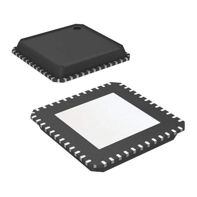
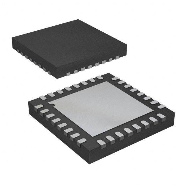
ICGOO电子元器件商城为您提供ADS1158IRTCT由Texas Instruments设计生产,在icgoo商城现货销售,并且可以通过原厂、代理商等渠道进行代购。 ADS1158IRTCT价格参考¥52.18-¥87.03。Texas InstrumentsADS1158IRTCT封装/规格:数据采集 - 模数转换器, 16 Bit Analog to Digital Converter 8, 16 Input 1 Sigma-Delta 48-VQFN-EP (7x7)。您可以下载ADS1158IRTCT参考资料、Datasheet数据手册功能说明书,资料中有ADS1158IRTCT 详细功能的应用电路图电压和使用方法及教程。
Texas Instruments(德州仪器)的ADS1158IRTCT是一款高精度、低功耗的24位模数转换器(ADC),属于数据采集系统中的关键组件。它具有多个应用场景,尤其是在需要高分辨率和精确测量的领域。

 1. 工业自动化与控制
在工业环境中,ADS1158IRTCT可以用于监测和控制各种传感器输出,如温度、压力、湿度等。其高分辨率和低噪声特性使得它可以精确地捕捉微小的信号变化,确保工业过程的稳定性和可靠性。例如,在精密制造中,它可以帮助监控生产设备的工作状态,及时发现异常情况并进行调整。

 2. 医疗设备
医疗设备对数据采集的精度要求极高,特别是在心电图(ECG)、脑电图(EEG)等生物电信号的测量中。ADS1158IRTCT能够提供高精度的数据采集,确保医生能够准确诊断患者的健康状况。此外,它还可以应用于便携式医疗设备中,如血糖仪、血压计等,帮助患者在家中进行自我监测。

 3. 环境监测
环境监测系统需要长时间、高精度地采集各种环境参数,如空气质量、水质、土壤湿度等。ADS1158IRTCT的低功耗特性使其非常适合用于这些长时间运行的监测设备,确保数据的连续性和准确性。它可以在偏远地区或难以维护的环境中长期工作,为环境保护和科学研究提供可靠的数据支持。

 4. 能源管理
在智能电网和能源管理系统中,ADS1158IRTCT可以用于监测电力系统的电压、电流等参数,帮助优化能源分配和提高能效。它还可以应用于太阳能、风能等可再生能源的发电系统中,实时监控发电效率,确保系统的稳定运行。

 5. 农业物联网
现代农业越来越多地依赖于精准农业技术,ADS1158IRTCT可以用于土壤湿度、温度、养分含量等参数的监测,帮助农民实现精细化管理,提高农作物产量和质量。此外,它还可以应用于牲畜健康监测系统中,实时跟踪牲畜的生理指标,预防疾病的发生。

总之,ADS1158IRTCT凭借其高精度、低功耗和多通道的特点,广泛应用于工业、医疗、环境、能源和农业等多个领域,满足了不同场景下的数据采集需求。
| 参数 | 数值 |
| 产品目录 | 集成电路 (IC)半导体 |
| 描述 | IC ADC 16BIT SER 125K 48VQFN模数转换器 - ADC 16B 16Ch 125kSPS Delta Sigma ADC |
| 产品分类 | |
| 品牌 | Texas Instruments |
| 产品手册 | |
| 产品图片 |
|
| rohs | 符合RoHS无铅 / 符合限制有害物质指令(RoHS)规范要求 |
| 产品系列 | 数据转换器IC,模数转换器 - ADC,Texas Instruments ADS1158IRTCT- |
| 数据手册 | |
| 产品型号 | ADS1158IRTCT |
| PCN封装 | |
| 产品培训模块 | http://www.digikey.cn/PTM/IndividualPTM.page?site=cn&lang=zhs&ptm=13240 |
| 产品目录页面 | |
| 产品种类 | 模数转换器 - ADC |
| 位数 | 16 |
| 供应商器件封装 | 48-VQFN 裸露焊盘(7x7) |
| 信噪比 | Yes |
| 其它名称 | 296-23494-1 |
| 分辨率 | 16 bit |
| 制造商产品页 | http://www.ti.com/general/docs/suppproductinfo.tsp?distId=10&orderablePartNumber=ADS1158IRTCT |
| 包装 | Digi-Reel® |
| 商标 | Texas Instruments |
| 安装类型 | 表面贴装 |
| 安装风格 | SMD/SMT |
| 封装 | Reel |
| 封装/外壳 | 48-VFQFN 裸露焊盘 |
| 封装/箱体 | VQFNP-48 |
| 工作温度 | -40°C ~ 105°C |
| 工作电源电压 | +/- 2.5 V, + 5 V |
| 工厂包装数量 | 250 |
| 接口类型 | Serial, SPI |
| 数据接口 | SPI |
| 最大功率耗散 | 62 mW |
| 最大工作温度 | + 105 C |
| 最小工作温度 | - 40 C |
| 标准包装 | 1 |
| 特性 | - |
| 电压参考 | Internal, External |
| 电压源 | 模拟和数字,双 ± |
| 系列 | ADS1158 |
| 结构 | Sigma-Delta |
| 视频文件 | http://www.digikey.cn/classic/video.aspx?PlayerID=1364138032001&width=640&height=455&videoID=44659313001 |
| 转换器数 | 1 |
| 转换器数量 | 1 |
| 转换速率 | 125 kS/s |
| 输入数和类型 | 16 个单端,单极16 个单端,双极8 个差分,单极8 个差分,双极 |
| 输入类型 | Single-Ended/Differential |
| 通道数量 | 16 Channel/8 Channel |
| 采样率(每秒) | 23.74k,125k |


- 商务部:美国ITC正式对集成电路等产品启动337调查
- 曝三星4nm工艺存在良率问题 高通将骁龙8 Gen1或转产台积电
- 太阳诱电将投资9.5亿元在常州建新厂生产MLCC 预计2023年完工
- 英特尔发布欧洲新工厂建设计划 深化IDM 2.0 战略
- 台积电先进制程称霸业界 有大客户加持明年业绩稳了
- 达到5530亿美元!SIA预计今年全球半导体销售额将创下新高
- 英特尔拟将自动驾驶子公司Mobileye上市 估值或超500亿美元
- 三星加码芯片和SET,合并消费电子和移动部门,撤换高东真等 CEO
- 三星电子宣布重大人事变动 还合并消费电子和移动部门
- 海关总署:前11个月进口集成电路产品价值2.52万亿元 增长14.8%


PDF Datasheet 数据手册内容提取
ADS1158 ADS1158 www.ti.com SBAS429D–JUNE2008–REVISEDMARCH2011 16-Channel, 16-Bit Analog-to-Digital Converter CheckforSamples:ADS1158 FEATURES DESCRIPTION 1 • 16Bits,NoMissingCodes The ADS1158 is a 16-channel (multiplexed), 23 low-noise, 16-bit, delta-sigma (ΔΣ) analog-to-digital • Fixed-ChannelorAutomaticChannelScan converter (ADC) that provides single-cycle settled • Fixed-ChannelDataRate:125kSPS data at channel scan rates from 1.8k to 23.7k • Auto-ScanDataRate:23.7kSPS/Channel samples per second (SPS) per channel. A flexible input multiplexer accepts combinations of eight • Single-ConversionSettledData differential or 16 single-ended inputs with a full-scale • 16Single-Endedor8DifferentialInputs differential range of 5V or true bipolar range of ±2.5V • Unipolar(+5V)orBipolar(±2.5V)Operation when operating with a 5V reference. The fourth-order delta-sigma modulator is followed by a fifth-order sinc • 0.3LSB(INL) digitalfilteroptimizedforlow-noiseperformance. • DCStability: 1μV/°COffsetDrift,2ppm/°CGainDrift The differential output of the multiplexer is accessible to allow signal conditioning before the input of the • Open-SensorDetection ADC. Internal system monitor registers provide • ConversionControlPin supply voltage, temperature, reference voltage, gain, • MultiplexerOutputforExternalSignal andoffsetdata. Conditioning An onboard PLL generates the system clock from a • On-ChipTemperature,Reference,Offset,Gain, 32.768kHz crystal, or can be overridden by an andSupplyVoltageReadback external clock source. A buffered system clock output (15.7MHz) is provided to drive a microcontroller or • 42mWPowerDissipation additionalconverters. • Standby,Sleep,andPower-DownModes Serial digital communication is handled via an • EightGeneral-PurposeInputs/Outputs(GPIO) SPI™-compatible interface. A simple command word • 32.768kHzCrystalOscillatororExternalClock structure controls channel configuration, data rates, digitalI/O,monitorfunctions,etc. APPLICATIONS Programmable sensor bias current sources can be • Medical,Avionics,andProcessControl usedtobiassensorsorverifysensorintegrity. • MachineandSystemMonitoring The ADS1158 operates from a unipolar +5V or • FastScanMulti-ChannelInstrumentation bipolar ±2.5V analog supply and a digital supply • IndustrialSystems compatible with interfaces ranging from 2.7V to 5.25V. The ADS1158 is available in a QFN-48 • TestandMeasurementSystems package. AVDD VREF DVDD GPIO[7:0] Internal ADS1158 Monitoring GPIO 1 CS 16-Bit Digital SPI DRDY Analog Inputs ¼ A1n6a:l1og ADC Filter Interface SDCINLK Input DOUT MUX 16 START Oscillator Control RESET AINCOM PWDN AVSS MUX ADC Ext CLK 32.768kHz DGND OUT IN In/Out 1 Pleasebeawarethatanimportantnoticeconcerningavailability,standardwarranty,anduseincriticalapplicationsofTexas Instrumentssemiconductorproductsanddisclaimerstheretoappearsattheendofthisdatasheet. SPIisatrademarkofMotorola,Inc. 2 Allothertrademarksarethepropertyoftheirrespectiveowners. 3 PRODUCTIONDATAinformationiscurrentasofpublicationdate. Copyright©2008–2011,TexasInstrumentsIncorporated Products conform to specifications per the terms of the Texas Instruments standard warranty. Production processing does not necessarilyincludetestingofallparameters.
ADS1158 SBAS429D–JUNE2008–REVISEDMARCH2011 www.ti.com This integrated circuit can be damaged by ESD. Texas Instruments recommends that all integrated circuits be handled with appropriateprecautions.Failuretoobserveproperhandlingandinstallationprocedurescancausedamage. ESDdamagecanrangefromsubtleperformancedegradationtocompletedevicefailure.Precisionintegratedcircuitsmaybemore susceptibletodamagebecauseverysmallparametricchangescouldcausethedevicenottomeetitspublishedspecifications. ORDERING INFORMATION For the most current package and ordering information see the Package Option Addendum at the end of this document,orseetheTIwebsiteatwww.ti.com. ABSOLUTE MAXIMUM RATINGS Overoperatingfree-airtemperaturerange,unlessotherwisenoted.(1) ADS1158 UNIT AVDDtoAVSS –0.3to+5.5 V AVSStoDGND –2.8to+0.3 V DVDDtoDGND –0.3to+5.5 V Inputcurrent 100,momentary mA Inputcurrent 10,continuous mA Analoginputvoltage AVSS–0.3toAVDD+0.3 V DigitalinputvoltagetoDGND –0.3toDVDD+0.3 V Maximumjunctiontemperature +150 °C Operatingtemperaturerange –40to+105 °C Storagetemperaturerange –60to+150 °C (1) Stressesabovetheseratingsmaycausepermanentdamage.Exposuretoabsolutemaximumconditionsforextendedperiodsmay degradedevicereliability.Thesearestressratingsonly,andfunctionaloperationofthedeviceattheseoranyotherconditionsbeyond thosespecifiedisnotimplied. 2 SubmitDocumentationFeedback Copyright©2008–2011,TexasInstrumentsIncorporated ProductFolderLink(s):ADS1158
ADS1158 www.ti.com SBAS429D–JUNE2008–REVISEDMARCH2011 ELECTRICAL CHARACTERISTICS AllspecificationsatT =–40°Cto+105°C,AVDD=+2.5V,AVSS=–2.5V,DVDD=+3.3V,f =16MHz(externalclock)orf = A CLK CLK 15.729MHz(internalclock),OPA227bufferbetweenMUXoutputsandADCinputs,V =+4.096V,andVREFN=–2.5V,unlessotherwise REF noted. ADS1158 PARAMETER CONDITIONS MIN TYP MAX UNIT ANALOGMULTIPLEXERINPUTS AIN0–AIN15, Absoluteinputvoltage AVSS–100mV AVDD+100mV V AINCOMwithrespecttoDGND On-channelresistance 80 Ω Crosstalk fIN=1kHz –110 dB SBCS[1:0]=01 1.5 Sensorbias(currentsource) μA SBCS[1:0]=11 24 1.5μA:24μAratioerror 1 % ADCINPUT Full-scaleinputvoltage (VIN=ADCINP–ADCINN) ±1.06VREF V Absoluteinputvoltage (ADCINP,ADCINN) AVSS–100mV AVDD+100mV V Differentialinputimpedance 65 kΩ SYSTEMPERFORMANCE Resolution Nomissingcodes 16 Bits Datarate,fixed-channelmode 1.953 125 kSPS Datarate,auto-scanmode 1.805 23.739 kSPS Integralnonlinearity(INL)(1) Differentialinput 0.3 1 LSB(2) Offseterror Choppingon Shortedinputs –1 –0.5(3) 0 LSB Offsetdrift Shortedinputs 1 μV/°C Gainerror 0.1 0.5 % Gaindrift 2 ppm/°C Noise 0.6 LSB(PP) Common-moderejection fCM=60Hz 100 dB AVDD,AVSS 85 Power-supplyrejection fPS=60Hz dB DVDD 95 VOLTAGEREFERENCEINPUT Referenceinputvoltage (VREF=VREFP–VREFN) 0.5 4.096 AVDD–AVSS V Negativereferenceinput(VREFN) AVSS–0.1V VREFP–0.5 V Positivereferenceinput(VREFP) VREFN+0.5 AVDD+0.1V V Referenceinputimpedance 40 kΩ SYSTEMPARAMETERS Externalreferencereadingerror 1 3 % Analogsupplyreadingerror 1 5 % Voltage TA=+25°C 168 mV Temperaturesensorreading 394(4) μV/°C Coefficient 563(5) μV/°C (1) Beststraightlinefitmethod. (2) FSR=Full-scalerange=2.13V . REF (3) Systematic–0.5LSBinreadingcode. (4) ADS1158temperatureforcedalone,testPCBinfreeair. (5) ADS1158andtestPCBtemperaturesforcedtogether. Copyright©2008–2011,TexasInstrumentsIncorporated SubmitDocumentationFeedback 3 ProductFolderLink(s):ADS1158
ADS1158 SBAS429D–JUNE2008–REVISEDMARCH2011 www.ti.com ELECTRICAL CHARACTERISTICS (continued) AllspecificationsatT =–40°Cto+105°C,AVDD=+2.5V,AVSS=–2.5V,DVDD=+3.3V,f =16MHz(externalclock)or A CLK f =15.729MHz(internalclock),OPA227bufferbetweenMUXoutputsandADCinputs,V =+4.096V,andVREFN CLK REF =–2.5V,unlessotherwisenoted. ADS1158 PARAMETER CONDITIONS MIN TYP MAX UNIT DIGITALINPUT/OUTPUT VIH 0.7DVDD DVDD V VIL DGND 0.3DVDD V Logiclevels VOH IOH=2mA 0.8DVDD DVDD V VOL IOL=2mA DGND 0.2DVDD V Inputleakage VIN=DVDD,GND 10 μA Frequency 0.1 16 MHz Masterclockinput(CLKIO) Dutycycle 40 60 % Crystalfrequency 32.768 kHz Crystaloscillator Clockoutputfrequency 15.729 MHz (seeCrystalOscillatorsection) Start-uptime(clockoutputvalid) 150 ms Clockoutputdutycycle 40 60 % POWERSUPPLY DVDD 2.7 5.25 V AVSS –2.6 0 V AVDD AVSS+4.75 AVSS+5.25 V Externalclock 0.25 0.6 mA operation Internaloscillator operation,clock 0.04 mA DVDDsupplycurrent outputdisabled Internaloscillator operation,clock 1.4 mA outputenabled(6) Power-down(7) 1 25 µA Converting 8.2 12 mA Standby 5.6 mA AVDD,AVSSsupplycurrent Sleep 2.1 mA Power-down 2 200 µA Converting 42 62 mW Standby 29 mW Powerdissipation Sleep 11 mW Power-down 14 μW (6) CLKIOload=20pF. (7) NoclockappliedtoCLKIO. 4 SubmitDocumentationFeedback Copyright©2008–2011,TexasInstrumentsIncorporated ProductFolderLink(s):ADS1158
ADS1158 www.ti.com SBAS429D–JUNE2008–REVISEDMARCH2011 PIN CONFIGURATION QFNPACKAGE (TOPVIEW) P N UT UT P N 4 5 6 7 XO XO CIN CIN 8 9 10 11 N N N N U U D D N N N N AI AI AI AI M M A A AI AI AI AI 48 47 46 45 44 43 42 41 40 39 38 37 AIN3 1 36 AIN12 AIN2 2 35 AIN13 AIN1 3 34 AIN14 AIN0 4 33 AIN15 AVSS 5 32 AINCOM AVDD 6 31 VREFP ADS1158 PLLCAP 7 30 VREFN XTAL1 8 29 DGND XTAL2 9 28 DVDD PWDN 10 27 CS RESET 11 26 START CLKSEL 12 25 DRDY 13 14 15 16 17 18 19 20 21 22 23 24 CLKIO GPIO0 GPIO1 GPIO2 GPIO3 GPIO4 GPIO5 GPIO6 GPIO7 SCLK DIN DOUT PINASSIGNMENTS ANALOG/DIGITAL PIN# NAME INPUT/OUTPUT DESCRIPTION 1 AIN3 Analoginput Analoginput3:single-endedchannel3,differentialchannel1(–) 2 AIN2 Analoginput Analoginput2:single-endedchannel2,differentialchannel1(+) 3 AIN1 Analoginput Analoginput1:single-endedchannel1,differentialchannel0(–) 4 AIN0 Analoginput Analoginput0:single-endedchannel0,differentialchannel0(+) Negativeanalogpowersupply:0Vforunipolaroperation,–2.5Vforbipolaroperation. 5 AVSS Analog (InternallyconnectedtoexposedthermalpadofQFNpackage.) 6 AVDD Analog Positiveanalogpowersupply:+5Vforunipolaroperation,+2.5Vforbipolaroperation. 7 PLLCAP Analog PLLbypasscapacitor:connect22nFcapacitortoAVSSwhenusingcrystaloscillator. 8 XTAL1 Analog 32.768kHzcrystaloscillatorinput1;seeCrystalOscillatorsection. 9 XTAL2 Analog 32.768kHzcrystaloscillatorinput2;seeCrystalOscillatorsection. 10 PWDN Digitalinput Power-downinput:holdlowforminimumoftwofCLKcyclestoengagelow-powermode. 11 RESET Digitalinput Resetinput:holdlowforminimumoftwofCLKcyclestoresetthedevice. 12 CLKSEL Digitalinput Clockselectinput:Low=activatescrystaloscillator,fCLKoutputonCLKIO. High=disablescrystaloscillator,applyfCLKtoCLKIO. 13 CLKIO DigitalI/O Systemclockinput/output(seeCLKSELpin) 14 GPIO0 DigitalI/O General-purposedigitalinput/output0 15 GPIO1 DigitalI/O General-purposedigitalinput/output1 16 GPIO2 DigitalI/O General-purposedigitalinput/output2 17 GPIO3 DigitalI/O General-purposedigitalinput/output3 18 GPIO4 DigitalI/O General-purposedigitalinput/output4 19 GPIO5 DigitalI/O General-purposedigitalinput/output5 20 GPIO6 DigitalI/O General-purposedigitalinput/output6 Copyright©2008–2011,TexasInstrumentsIncorporated SubmitDocumentationFeedback 5 ProductFolderLink(s):ADS1158
ADS1158 SBAS429D–JUNE2008–REVISEDMARCH2011 www.ti.com PINASSIGNMENTS (continued) ANALOG/DIGITAL PIN# NAME INPUT/OUTPUT DESCRIPTION 21 GPIO7 DigitalI/O General-purposedigitalinput/output7 22 SCLK Digitalinput SPIinterfaceclockinput:dataclockedinonrisingedge,clockedoutonfallingedge. 23 DIN Digitalinput SPIinterfacedatainput:dataareinputtothedevice. 24 DOUT Digitaloutput SPIinterfacedataoutput:dataareoutputfromthedevice. 25 DRDY Digitaloutput Datareadyoutput:activelow. 26 START Digitalinput Startconversioninput:activehigh. 27 CS Digitalinput SPIinterfacechipselectinput:activelow. 28 DVDD Digital Digitalpowersupply:2.7Vto5.25V 29 DGND Digital Digitalground 30 VREFN Analoginput Referenceinputnegative 31 VREFP Analoginput Referenceinputpositive 32 AINCOM Analoginput Analoginputcommon:commoninputpintoallsingle-endedinputs. 33 AIN15 Analoginput Analoginput15:single-endedchannel15,differentialchannel7(–) 34 AIN14 Analoginput Analoginput14:single-endedchannel14,differentialchannel7(+) 35 AIN13 Analoginput Analoginput13:single-endedchannel13,differentialchannel6(–) 36 AIN12 Analoginput Analoginput12:single-endedchannel12,differentialchannel6(+) 37 AIN11 Analoginput Analoginput11:single-endedchannel11,differentialchannel5(–) 38 AIN10 Analoginput Analoginput10:single-endedchannel10,differentialchannel5(+) 39 AIN9 Analoginput Analoginput9:single-endedchannel9,differentialchannel4(–) 40 AIN8 Analoginput Analoginput8:single-endedchannel8,differentialchannel4(+) 41 ADCINN Analoginput ADCdifferentialinput(–) 42 ADCINP Analoginput ADCdifferentialinput(+) 43 MUXOUTN Analogoutput Multiplexerdifferentialoutput(–) 44 MUXOUTP Analogoutput Multiplexerdifferentialoutput(+) 45 AIN7 Analoginput Analoginput7:single-endedchannel7,differentialchannel3(–) 46 AIN6 Analoginput Analoginput6:single-endedchannel6,differentialchannel3(+) 47 AIN5 Analoginput Analoginput5:single-endedchannel5,differentialchannel2(–) 48 AIN4 Analoginput Analoginput4:single-endedchannel4,differentialchannel2(+) 6 SubmitDocumentationFeedback Copyright©2008–2011,TexasInstrumentsIncorporated ProductFolderLink(s):ADS1158
ADS1158 www.ti.com SBAS429D–JUNE2008–REVISEDMARCH2011 PARAMETER MEASUREMENT INFORMATION CS(1) tCSPW tCSSC tSCLK t SPW SCLK tDIST tSPW DIN tDIHD tDOPD Hi-Z Hi-Z DOUT t t CSDO DOHD (1) CScanbetiedlow. Figure1. SerialInterfaceTiming SERIALINTERFACETIMINGCHARACTERISTICS AtT =–40°Cto+105°CandDVDD=2.7Vto5.25V,unlessotherwisenoted. A SYMBOL DESCRIPTION MIN MAX UNITS t SCLKperiod 2 τ (1) SCLK CLK t SCLKhighorlowpulsewidth(exceedingmaxresetsSPIinterface) 0.8 4096(2) τ SPW CLK t CSlowtofirstSCLK:setuptime(3) 2.5 τ CSSC CLK t ValidDINtoSCLKrisingedge:setuptime 10 ns DIST t ValidDINtoSCLKrisingedge:holdtime 5 ns DIHD t SCLKfallingedgetovalidnewDOUT:propagationdelay(4) 20 ns DOPD t SCLKfallingedgetooldDOUTinvalid:holdtime 0 ns DOHD t CShightoDOUTinvalid(3-state) 5 τ CSDO CLK t CSpulsewidthhigh 2 τ CSPW CLK (1) τ =masterclockperiod=1/f . CLK CLK (2) Programmableto256τ . CLK (3) CScanbetiedlow. (4) DOUTload=20pF||100kΩtoDGND. t DRDY DRDY tDDO DOUT Figure2. DRDYUpdateTiming DRDYUPDATETIMINGCHARACTERISTICS SYMBOL DESCRIPTION TYP UNITS t DRDYhighpulsewidthwithoutdataread 1 τ DRDY CLK t ValidDOUTtoDRDYfallingedge(CS=0) 0.5 τ DDO CLK Copyright©2008–2011,TexasInstrumentsIncorporated SubmitDocumentationFeedback 7 ProductFolderLink(s):ADS1158
ADS1158 SBAS429D–JUNE2008–REVISEDMARCH2011 www.ti.com TYPICAL CHARACTERISTICS AtT =+25°C,AVDD=+2.5V,AVSS=–2.5V,DVDD=+3.3V,f =16MHz(externalclock)orf =15.729MHz(internalclock),OPA227 A CLK CLK bufferbetweenMUXoutputsandADCinputs,VREFP=+2.048V,andVREFN=–2.048V,unlessotherwisenoted. OFFSETWITH0.5VREFERENCE,CHOPPINGON OFFSETWITH4.096VREFERENCE,CHOPPINGON 6000 3500 25 Units, 25 Units, 256 Samples/Unit 254 Samples/Unit 5000 3000 s s e e c c 2500 en 4000 en curr curr 2000 c c O 3000 O of of 1500 er er b 2000 b m m 1000 u u N N 1000 500 0 0 -4 -3 -2 -1 0 1 2 3 -2 -1 0 1 2 Offset (Output Code) Offset (Output Code) Figure3. Figure4. OFFSETvsTEMPERATURE GAINERRORHISTOGRAM 100 40 150 Units From Two Production Sets 50 35 V) CHOP = 1 es 30 Offset (m -500 ccurrenc 25 alized -100 CHOP = 0 er of O 2105 m b Nor -150 Num 10 -200 5 -250 0 -40 -15 10 35 60 85 110 00000000000000000000 00000000000000000000 Temperature (°C) 1234567891011121314151617181920 Absolute Gain Error (ppm) Figure5. Figure6. GAINDRIFTHISTOGRAM GAINERRORvsTEMPERATURE 30 60 150 Units From Two Production Sets 40 25 m) 20 ences 20 or (pp 0 urr Err -20 Occ 15 ain -40 mber of 10 alizedG --6800 u m N or -100 5 N -120 0 -140 8 3 7 1 5 9 3 3 9 5 1 7 3 8 -40 -15 10 35 60 85 110 -3. -3. -2. -2. -1. -0. -0. 0. 0. 1. 2. 2. 3. 3. Temperature (°C) Gain Drift (ppm/°C) Figure7. Figure8. 8 SubmitDocumentationFeedback Copyright©2008–2011,TexasInstrumentsIncorporated ProductFolderLink(s):ADS1158
ADS1158 www.ti.com SBAS429D–JUNE2008–REVISEDMARCH2011 TYPICAL CHARACTERISTICS (continued) AtT =+25°C,AVDD=+2.5V,AVSS=–2.5V,DVDD=+3.3V,f =16MHz(externalclock)orf =15.729MHz(internal A CLK CLK clock),OPA227bufferbetweenMUXoutputsandADCinputs,VREFP=+2.048V,andVREFN=–2.048V,unlessotherwise noted. INTEGRALNONLINEARITYvsV INTEGRALNONLINEARITYvsINPUTLEVEL REF 10 8 V = 4.096V 9 6 REF 8 m) 7 m) 4 p p or (p 6 or (p 2 Err 5 Err 0 y y arit 4 arit -2 e e n 3 n Li 2 Li -4 TA=-40°C TA= +55°C 1 -6 TA=-10°C TA= +85°C T = +25°C T = +105°C 0 -8 A A 0.5 1.0 1.5 2.0 2.5 3.0 3.5 4.0 4.5 5.0 -5 -4 -3 -2 -1 0 1 2 3 4 5 V (V) V (V) REF IN Figure9. Figure10. INLvsTEMPERATURE OUTPUTSPECTRUM 7 0 f = 1kHz,-0.5dBFS -20 6 DRATE[1:0] = 11 -40 32768 Points 5 -60 INL (ppm) 43 Level(dBFS) --11-028000 2 -140 -160 1 -180 0 -200 -40 -15 10 35 60 85 110 1 10 100 1k 10k 100k Temperature (°C) Frequency (Hz) Figure11. Figure12. TEMPERATURESENSORVOLTAGEvsTEMPERATURE TEMPERATURESENSORREADINGHISTOGRAM 220 8 ADS1158 and Test PCB Temperatures 35 Units From Two Production Sets V) 210 Forced Together 7 m Voltage ( 211098000 urrences 65 nsor 170 Occ 4 perature Se 111654000 ATeDsSt 1P1C5B8 iOn nFlrye Tee Amirperature Forced, Number of 32 m Te 130 1 120 0 -40 -20 0 20 40 60 80 100 120 15161718192021222324252627282930313233343536373839 Temperature (°C) Temperature Reading (°C) Figure13. Figure14. Copyright©2008–2011,TexasInstrumentsIncorporated SubmitDocumentationFeedback 9 ProductFolderLink(s):ADS1158
ADS1158 SBAS429D–JUNE2008–REVISEDMARCH2011 www.ti.com TYPICAL CHARACTERISTICS (continued) AtT =+25°C,AVDD=+2.5V,AVSS=–2.5V,DVDD=+3.3V,f =16MHz(externalclock)orf =15.729MHz(internal A CLK CLK clock),OPA227bufferbetweenMUXoutputsandADCinputs,VREFP=+2.048V,andVREFN=–2.048V,unlessotherwise noted. SENSORBIASCURRENTSOURCERATIOvs SENSORBIASCURRENTSOURCERATIOHISTOGRAM TEMPERATURE 14 18.0 25 Units From 12 One Production Lot 17.5 es 17.0 c 10 n Occurre 8 A/A)mm 1166..50 ber of 6 Ratio ( 15.5 m 4 u 15.0 N 2 14.5 0 14.0 14.0 14.5 15.0 15.516.0 16.5 17.0 17.5 18.018.5 19.0 -40 -15 10 35 60 85 110 Ratio (mA/mA) Temperature (°C) Figure15. Figure16. SUPPLYCURRENTvsTEMPERATURE POWER-DOWNCURRENTvsTEMPERATURE 10 1.0 4 Unipolar AVDD/AVSS AVSS = 0V, AVDD = 5V A) 8 0.8 m 3 VDD/AVSS Current ( 64 00..64 DVDD Current (mA) Current (A)m 21 A 2 0.2 DVDD AVSS/AVDD 0 0 0 -40 -15 10 35 60 85 110 -40 -15 10 35 60 85 110 Temperature (°C) Temperature (°C) Figure17. Figure18. POWER-DOWNCURRENTvsTEMPERATURE 140 Bipolar AVSS =-2.5V, AVDD = 2.5V 120 100 A) AVSS m 80 nt ( e urr 60 C 40 20 AVDD 0 -40 -15 10 35 60 85 110 Temperature (°C) Figure19. 10 SubmitDocumentationFeedback Copyright©2008–2011,TexasInstrumentsIncorporated ProductFolderLink(s):ADS1158
ADS1158 www.ti.com SBAS429D–JUNE2008–REVISEDMARCH2011 OVERVIEW The ADS1158 is a flexible, 16-bit, low-noise ADC The ADS1158 converter consists of a fourth-order, optimized for fast multi-channel, high-resolution delta-sigma modulator followed by a programmable measurement systems. The converter provides a digital filter. The modulator measures the differential maximum channel scan rate of 23.7kSPS, giving a input signal, V = (ADCINP – ADCINN), against the IN complete16-channelscaninlessthan700μs. differential reference input, V = (VREFP – REF VREFN). The digital filter receives the modulator Figure 20 shows the block diagram of the ADS1158. signal and provides a low-noise digital output. The The input multiplexer selects which analog input pins ADC channel block controls the multiplexer connect to the multiplexer output pins Auto-Scan feature. Channel Auto-Scan occurs at a (MUXOUTP/MUXOUTN). External signal conditioning maximum rate of 23.7kSPS. Slower scan rates can can be used between the multiplexer output pins and beusedwithcorrespondingincreasesinresolution. the ADC input pins (ADCINP/ADCINN) or the multiplexer output can be routed internally to the ADC Communication is handled over an SPI-compatible inputs without external circuitry. Selectable current serial interface with a set of simple commands to sources within the input multiplexer can be used to control the ADS1158. Onboard registers store the bias sensors or detect for a failed sensor. On-chip various settings for the input multiplexer, sensor system function readings provide readback of detect bias, data rate selection, etc. Either an temperature,supplyvoltage,gain,offset,andexternal external 32.768kHz crystal, connected to pins XTAL1 reference. andXTAL2,oranexternalclockappliedtopinCLKIO can be used as the clock source. When using the external crystal oscillator, the system clock is available as an output for driving other devices or controllers. General-purpose digital I/Os (GPIO) provideinputandoutputcontrolofeightpins. AVDD DVDD GPIO[7:0] CLKIO CLKSEL PLLCAP XTAL2 XTAL1 Clock Control GPIO AIN0 Sensor AIN1 Bias CS AIN2 SPI SCLK AIN3 Interface DIN AIN4 DOUT AIN5 Supply Monitor Temperature AIN6 DRDY AIN7 Control PWDN 16-Channel AIN8 ADC Channel Control Logic RESET MUX AIN9 START AIN10 Internal Ref AIN11 AIN12 Ext Ref Monitor AIN13 AIN14 ADC Digital Filter AIN15 AINCOM AVSS MUXOUTP MUXOUTN ADCINP ADCINN VREFN VREFP GND Figure20. ADS1158BlockDiagram Copyright©2008–2011,TexasInstrumentsIncorporated SubmitDocumentationFeedback 11 ProductFolderLink(s):ADS1158
ADS1158 SBAS429D–JUNE2008–REVISEDMARCH2011 www.ti.com MULTIPLEXER INPUTS The load presented by the switched capacitor can be modeledwithaneffectiveresistance(R )of40kΩ for A simplified diagram of the input multiplexer is eff f = 16MHz. Note that the effective impedance of illustrated in Figure 22. The multiplexer connects one CLK the reference inputs loads an external reference with of 16 single-ended external inputs, one of eight anon-zerosourceimpedance. differential external inputs, or one of the on-chip internalvariablestotheADCinputs.Theoutputofthe AVDD channel multiplexer can be routed to external pins and then to the input of the ADC. This flexibility allows for use of external signal conditioning. See the ExternalMultiplexerLoopsection. ESD Diodes Electrostatic discharge (ESD) diodes protect the analog inputs. To keep these diodes from turning on, VREFP make sure the voltages on the input pins do not go below AVSS by more than 100mV, and likewise do 3pF Reff= 40kW notexceedAVDDbymorethan100mV: (f = 16MHz) CLK VREFN AVSS– 100mV <(AnalogInputs)< AVDD+100mV. ESD Overdriving the multiplexer inputs may affect the Diodes conversions of other channels. See the Input Overload Protection description in the Hardware ConsiderationssegmentoftheApplicationssection. AVSS The converter supports two modes of channel access through the multiplexer: the Auto-Scan mode and the Figure21. SimplifiedReferenceInputCircuit Fixed-Channel mode. These modes are selected by the MUXMOD bit of register CONFIG0. The ESD diodes protect the reference inputs. To keep Auto-Scan mode scans through the selected these diodes from turning on, make sure the voltages channels automatically, with break-before-make on the reference pins do not go below AVSS by more switching. The Fixed-Channel mode requires the user than 100mV, and likewise do not exceed AVDD by to set the channel address for each channel 100mV: measured. AVSS-100mV < (VREFP or VREFN) < AVDD + 100mV A high-quality reference voltage is essential to VOLTAGE REFERENCE INPUTS achieve the best performance from the ADS1158. (VREFP, VREFN) Noise and drift on the reference degrade overall The voltage reference for the ADS1158 ADC is the system performance. It is especially critical that differential voltage between VREFP and VREFN: special care be given to the circuitry that generates V = VREFP – VREFN. The reference inputs use a the reference voltages and the layout when operating REF structure similar to that of the analog inputs with the in the low-noise settings (that is, with low data rates) circuitry on the reference inputs shown in Figure 21. to prevent the voltage reference from limiting performance. See the Reference Inputs description in the Hardware Considerations segment of the Applicationssection. 12 SubmitDocumentationFeedback Copyright©2008–2011,TexasInstrumentsIncorporated ProductFolderLink(s):ADS1158
ADS1158 www.ti.com SBAS429D–JUNE2008–REVISEDMARCH2011 VREFP VREFN Multiplexer Reference/Gain Monitor AIN0 AIN1 AIN2 Temperature Sensor Monitor AVDD AIN3 1x 2x AIN4 AIN5 8x 1x AIN6 AVSS AIN7 Supply Monitor AIN8 AVDD AVSS AIN9 AIN10 AIN11 NOTE: ESD diodes not shown. AIN12 Internal AVSS Reference AIN13 AIN14 AIN15 ADC AINCOM AVSS AVDD (AVDD-AVSS)/2 Sensor Bias Offset Monitor P N P N T T N N UXOU UXOU ADCI ADCI M M Figure22. InputMultiplexer Copyright©2008–2011,TexasInstrumentsIncorporated SubmitDocumentationFeedback 13 ProductFolderLink(s):ADS1158
ADS1158 SBAS429D–JUNE2008–REVISEDMARCH2011 www.ti.com ADC INPUTS inputs. The average value of this current can be used to calculate an effective impedance (R ) where R = The ADS1158 ADC inputs (ADCINP, ADCINN) eff eff V /I . These impedances scale inversely with measure the input signal using internal capacitors IN AVERAGE f . For example, if f is reduced by a factor of that are continuously charged and discharged. The CLK CLK two,theimpedanceswilldouble. left side of Figure 24 shows a simplified schematic of the ADC input circuitry; the right side of Figure 24 As with the multiplexer and reference inputs, ESD shows the input circuitry with the capacitors and diodes protect the ADC inputs. To keep these diodes switches replaced by an equivalent circuit. Figure 23 from turning on, make sure the voltages on the input shows the ON/OFF timings of the switches shown in pins do not go below AVSS by more than 100mV, Figure 24. S switches close during the input and likewise do not exceed AVDD by more than 1 sampling phase. With S closed, C charges to 100mV. 1 A1 ADCINP, C charges to ADCINN, and C charges to A2 B (ADCINP – ADCINN). For the discharge phase, S1 tSAMPLE opensfirstandthenS2closes.CA1andCA2discharge ON to approximately AVSS + 1.3V and C discharges to S B 1 0V. This two-phase sample/discharge cycle repeats OFF withaperiodoft =2/f . SAMPLE CLK ON S Thechargingoftheinputcapacitorsdrawsatransient 2 OFF current from the source driving the ADS1158 ADC Figure23. S andS SwitchTimingforFigure24 1 2 AVSS + 1.3V AVSS + 1.3V S 2 CA1= 0.65pF ReffA= 190kW S 1 Equivalent ADCINP Circuit ADCINP CB= 1.6pF ReffB= 78kW (fCLK= 16MHz) S 1 ADCINN ADCINN CA2= 0.65pF ReffA= 190kW S 2 AVSS + 1.3V R = t /C AVSS + 1.3V eff SAMPLE X RAIN= ReffB|| 2ReffA NOTE: ESD input diodes not shown. Figure24. SimplifiedADCInputStructure 14 SubmitDocumentationFeedback Copyright©2008–2011,TexasInstrumentsIncorporated ProductFolderLink(s):ADS1158
ADS1158 www.ti.com SBAS429D–JUNE2008–REVISEDMARCH2011 MASTER CLOCK (f ) CLK 50W The ADS1158 oversamples the analog input at a high Clock Output CLKIO rate. This oversampling requires a high-frequency (15.729MHz) master clock to be supplied to the converter. As AVSS 0V to-2.5V shown in Figure 25, the clock comes from either an internal oscillator (with external crystal), or an CLKSEL XTAL1 XTAL2 PLLCAP externalclocksource. 32.768kHz(1) 22nF CLKENB Bit 4.7pF 4.7pF Internal Master Clock (fCLK) (1) Parallelresonanttype.CL=12.5pF,ESR=35kΩ(max).Place the crystal and load capacitors as close as possible to the device pins. MUX CLKIO Figure26. CrystalOscillatorConnection Table1.SystemClockSource Oscillator and PLL CLKSEL CLKENB PIN CLOCKSOURCE BIT CLKIOFUNCTION 32.768kHz Disabled CLKSEL XTAL1 XTAL2 PLL 0 0 crystaloscillator (internallygrounded) 32.768kHz Figure25. ClockGenerationBlockDiagram 0 1 Output(15.729MHz) crystaloscillator 1 Externalclockinput X Input(16MHz) The CLKSEL pin determines the source of the system clock, as shown in Table 1. The CLKIO pin Table2.ApprovedCrystalVendors functions as an input or as an output. When the VENDOR CRYSTALPRODUCT CLKSEL pin is set to '1', CLKIO is configured as an input to receive the master clock. When the CLKSEL Epson C-001R pin is set to '0', the crystal oscillator generates the Epson MC-30632.7680K-A0 clock. The CLKIO pin can then be configured to Epson FC-13532.7680KA-A0 output the master clock. When the clock output is not ECS ECS-.327-12.5-17-TR needed, it can be disabled to reduce device power consumption. ExternalClockInput CrystalOscillator When using an external clock to operate the device, apply the master clock to the CLKIO pin. For this An on-chip oscillator and phase-locked loop (PLL) mode, the CLKSEL pin is tied high. CLKIO then together with an external crystal can be used to becomesaninput,asshowninFigure27. generate the system clock. For this mode, tie the CLKSEL pin low. A 22nF PLL filter capacitor, connected from the PLLCAP pin to the AVSS pin, is 50W required. The internal clock of the PLL can be output Clock Input CLKIO to the CLKIO to drive other converters or controllers. (16MHz) If not used, disable the clock output to reduce device 2.7V DVDD power consumption; see Table 1 for settings. The to 5V clock output is enabled by a register bit setting CLKSEL XTAL1 XTAL2 PLLCAP (default is ON). Figure 26 shows the oscillator connections. Place these components as close to the No Connection pins as possible to avoid interference and coupling. Do not connect XTAL1 or XTAL2 to any other logic. Figure27. ExternalClockConnection The oscillator start-up time may vary, depending on the crystal and ambient temperature. The user should verifytheoscillatorstart-uptime. Copyright©2008–2011,TexasInstrumentsIncorporated SubmitDocumentationFeedback 15 ProductFolderLink(s):ADS1158
ADS1158 SBAS429D–JUNE2008–REVISEDMARCH2011 www.ti.com Make sure to use a clock source clean from jitter or DigitalFilter interference. Ringing or under/overshoot should be The programmable low-pass digital filter receives the avoided. A 50Ω resistor in series with the CLKIO pin modulator output and produces a high-resolution (placedclosetothesource)canoftenhelp. digital output. By adjusting the amount of filtering, tradeoffs can be made between resolution and data ADC rate—filter more for higher resolution, filter less for The ADC block of the ADS1158 is composed of two higher data rate. The filter consists of two sections, a blocks:amodulatorandadigitalfilter. fixed filter followed by a programmable filter. Figure 28 shows the block diagram of the filter. Data Modulator are supplied to the filter from the analog modulator at a rate of f /2. The fixed filter is a fifth-order sinc CLK The modulator converts the analog input voltage into filter with a decimation value of 64 that outputs data a pulse code modulated (PCM) data stream. When at a rate of f /128. The second stage of the filter is CLK the level of differential analog input (ADCINP – a programmable averager (first-order sinc filter) with ADCINN) is near the level of the reference voltage, thenumberofaveragessetbytheDRATE[1:0]bits. the '1' density of the PCM data stream is at its highest.Whenthelevelofthedifferentialanaloginput The data rate depends upon the system clock is near zero, the PCM '0' and '1' densities are nearly frequency (fCLK) and the converter configuration. The equal. The fourth-order modulator shifts the data rate can be computed by Equation 1 or quantization noise to a high frequency (out of the Equation2: passband)wherethedigitalfiltercaneasilyremoveit. Datarate(Auto-Scan): The modulator continuously chops the input, resulting f CLK in excellent offset and offset drift performance. It is important to note that offset or offset drift that 128(411b-DR+ 4.26525 + TD)´2CHOP (1) originates from the external circuitry is not removed Datarate(Fixed-Channelmode): by the modulator chopping. These errors can be f effectively removed by using the external chopping CLK feature of the ADS1158 (see the External Chopping 128[411b-DR+ CHOP(4.26525 + TD)]´2CHOP (2) section). Where: DR=DRATE[1:0]registerbits(binary). CHOP=Chopregisterbit. TD = time delay value given in Table 4 from the DLY[2:0]registerbits(128/f periods). CLK Modulator Rate = f /2 Data Rate = f /128 Data Rate(1)= f /(128´Num_Ave) CLK CLK CLK Analog sinc5 Programmable Modulator Filter Averager Num_Ave (1) DatarateforFixed-Channelmode,Chop=0,Delay=0. Figure28. BlockDiagramofDigitalFilter 16 SubmitDocumentationFeedback Copyright©2008–2011,TexasInstrumentsIncorporated ProductFolderLink(s):ADS1158
ADS1158 www.ti.com SBAS429D–JUNE2008–REVISEDMARCH2011 Table 3 shows a listing of the averaging and data Figure 30 shows the response with averaging set to 4 rates for each of the four DRATE[1:0] register (DRATE[1:0] = 10). 4-reading, post-averaging settings for the Auto-Scan and Fixed-Channel modes, produces three equally-spaced notches between with CHOP, DLY = 0. Note that the data rate scales each main notch of the sinc5 filter. The frequency directly with f . For example, reducing f by 2x responseofDRATE[1:0]=01and00followsasimilar CLK CLK reducesthemaximumdatarateby2x. pattern, but with 15 and 63 equally-spaced notches betweenthemainsinc5notches,respectively. FREQUENCY RESPONSE 0 The low-pass digital filter sets the overall frequency Data Rate response for the ADS1158. The filter response is the -20 Auto-Scan Mode product of the responses of the fixed and (23.739kSPS) programmable filter sections and is given by -40 Equation3: dB) -60 DFiaxtead R-Cahteannel Mode ½H(f)½=½Hsinc5(f)½´½HAverager(f)½= ain ( -80 (125kSPS) G 5 sin 128p´f sin 128p´Num_Ave´f -100 f f CLK ´ CLK -120 2p´f 128p´f 64´sin Num_Ave´sin -140 f f CLK CLK 0 125 250 375 500 625 (3) Frequency (kHz) The digital filter attenuates noise on the modulator Figure29. FrequencyResponse,DRATE[1:0]=11 output, including noise from within the ADS1158 and external noise present within the ADS1158 input signal. Adjusting the filtering by changing the number 0 of averages used in the programmable filter changes Data Rate the filter bandwidth. With a higher number of -20 Auto-Scan Mode averages, the bandwidth is reduced and more noise (15.123kSPS) isattenuated. -40 Data Rate The low-pass filter has notches (or zeros) at the data B) -60 Fixed-Channel Mode d output rate and multiples thereof. The sinc5 part of n ( (31.25kSPS) ai -80 the filter produces wide notches at f /128 and G CLK multiples thereof. At these frequencies, the filter has -100 zero gain. Figure 29 shows the response with no post averaging. Note that in Auto-Scan mode, the data -120 rate is reduced while retaining the same frequency -140 responseasinFixed-Channelmode. 0 125 250 375 500 625 With programmable averaging, the wide notches Frequency (kHz) produced by the sinc5 filter remain, but a number of narrow notches are superimposed in the response. Figure30. FrequencyResponse,DRATE[1:0]=10 The number of the superimposed notches is determined by the number of readings averaged(minusone). Table3.DataRates(1) DATARATEAUTO-SCAN DATARATEFIXED-CHANNEL –3dBBANDWIDTH DRATE[1:0] Num_Ave(2) MODE(SPS)(3) MODE(SPS) (Hz) 11 1 23739 125000 25390 10 4 15123 31250 12402 01 16 6168 7813 3418 00 64 1831 1953 869 (1) f =16MHz,Chop=0,andDelay=0. CLK (2) Num_Aveisthenumberofaveragesperformedbythedigitalfiltersecondstage. (3) InAuto-Scanmode,thedataratelistedisforasinglechannel;theeffectivedatarateformultiplechannels(onaper-channelbasis)is thevalueshowninFigure29andFigure30dividedbythenumberofactivechannelsinascanloop. Copyright©2008–2011,TexasInstrumentsIncorporated SubmitDocumentationFeedback 17 ProductFolderLink(s):ADS1158
ADS1158 SBAS429D–JUNE2008–REVISEDMARCH2011 www.ti.com ALIASING applying asynchronous step inputs, the settling time is somewhat different. The step-input settling time The digital filter low-pass characteristic repeats at diagrams (Figure 32 and Figure 33) show the multiples of the modulator rate of f /2. Figure 31 CLK converter step response with an asynchronous step shows the response plotted out to 16MHz at the data input. For most modes of operation, the analog input rate of 125kSPS (Fixed-Channel mode). Notice how must be stable for one complete conversion cycle to the responses near dc, 8MHz, and 16MHz are the provide settled data. In Fixed-Channel mode same. The digital filter attenuates high-frequency (DRATE[1:0] = 11), the input must be stable for five noise on the ADS1158 inputs up to the frequency completeconversioncycles. where the response repeats. However, noise or frequency components present on the analog input where the response repeats alias into the passband. Data Not Settled Settled Data For most applications, an anti-alias filter is recommended to remove this noise. A simple DRDY 1 2 first-order input filter with a pole at 200kHz provides–34dBrejectionatthefirstimagefrequency. Step Input 0 DRATE[1:0] = 11 Figure32. AsynchronousStep-InputSettling -20 125kSPS Time(DRATE[1:0]=10,01,00) Fixed-Channel Mode -40 B) -60 Data Not Settled Settled Data d n ( Gai -80 DRDY 1 2 6 -100 -120 Step Input -140 0 4 8 12 16 Figure33. AsynchronousStep-InputSettling Time(Fixed-ChannelMode,DRATE[1:0]=11) Frequency (MHz) Figure31. FrequencyResponseOutto16MHz Table4.EffectiveDataRateswithSwitch-Time Delay(Auto-ScanMode)(1) Referring to Figure 29 and Figure 30, frequencies TIME present on the analog input above the Nyquist rate DELAY TIME DRATE DRATE DRATE DRATE (sample rate/2) are first attenuated by the digital filter DLY (128/fCLK DELAY [1:0]= [1:0]= [1:0]= [1:0]= andthenaliasedintothepassband. [2:0] periods) (μS) 11 10 01 00 000 0 0 23739 15123 6168 1831 SETTLING TIME 001 1 8 19950 13491 5878 1805 010 2 16 17204 12177 5614 1779 The design of the ADS1158 provides fully-settled 011 4 32 13491 10191 5151 1730 data when scanning through the input channels in 100 8 64 9423 7685 4422 1639 Auto-Scan mode. The DRDY flag asserts low when the data for each channel are ready. It may be 101 16 128 5878 5151 3447 1483 necessary to use the automatic switch time delay 110 32 256 3354 3104 2392 1247 feature to provide time for settling of the external 111 48 384 2347 2222 1831 1075 buffer and associated components after channel switching. When the converter is started (START pin (1) Timedelayanddataratesscalewithf .IfChop=1,the transitions high or Start Command) with stable inputs, CLK dataratesarehalfthoseshown.f =16MHz,Auto-Scan CLK the first converter output is fully settled. When mode. 18 SubmitDocumentationFeedback Copyright©2008–2011,TexasInstrumentsIncorporated ProductFolderLink(s):ADS1158
ADS1158 www.ti.com SBAS429D–JUNE2008–REVISEDMARCH2011 EXTERNAL MULTIPLEXER LOOP Use of the switch time delay register reduces the effective channel data rate. Table 4 shows the actual The external multiplexer loop consists of two data rates derived from Equation 1, when using the differential multiplexer output pins and two differential switchtimedelayfeature. ADC input pins. The user may use external components (buffering/filtering, single-ended to When pulse converting, where one channel is differential conversion, etc.) to form a signal converted with each START pin pulse or each pulse conditioning loop. For best performance, the ADC command, the application software may provide the inputshouldbebufferedanddrivendifferentially. required time delay between pulses. However, with Chop = 1, the switch time delay feature may continue To bypass the external multiplexer loop, connect the tobenecessarytoallowforsettling. ADC input pins directly to the multiplexer output pins, or select internal bypass connection (BYPASS = 0 of In estimating the time delay that may be required, CONFIG0). Note that the multiplexer output pins are Table 5 lists the time delay-to-time constant ratio (t/τ) activeregardlessofthebypasssetting. and the corresponding final settled data in % and numberofbits. SWITCH TIME DELAY Table5.SettlingTime When using the ADS1158 in the Auto-Scan mode, where the converter automatically switches from one FINALSETTLING FINALSETTLING channel to the next, the settling time of the external t/τ(1) (%) (Bits) signal conditioning circuit becomes important. If the 1 63 2 channel does not fully settle after the multiplexer 3 95 5 channel is switched, the data may not be correct. The 5 99.3 7 ADS1158 provides a switch time delay feature which 7 99.9 10 automaticallyprovidesadelayafterchannelswitching to allow the channel to settle before taking a reading. 10 99.995 14 The amount of time delay required depends primarily 15 99.998 16 onthesettlingtimeoftheexternalsignalconditioning. (1) Multiple time constants can be approximated by: Additional consideration may be needed to account (τ 2+τ 2+…). 1 2 for the settling of the input source arising from the transientgeneratedfromchannelswitching. Copyright©2008–2011,TexasInstrumentsIncorporated SubmitDocumentationFeedback 19 ProductFolderLink(s):ADS1158
ADS1158 SBAS429D–JUNE2008–REVISEDMARCH2011 www.ti.com SENSOR BIAS The current source is connected to the output of the multiplexer. For unselected channels, the current An integrated current source provides a means to source is not connected. This configuration means bias an external sensor (for example, a diode that when a new channel is selected, the current junction); or, it verifies the integrity of a sensor or source charges stray sensor capacitance, which may sensor connection. When the sensor fails to an open slow the rise of the sensor voltage. The automatic condition, the current sources drive the inputs of the switch time delay feature can be used to apply an converter to positive full-scale. The biasing is in the appropriate time delay before a conversion is started form of differential currents (programmable 1.5μA or to provide fully settled data (see the Switch Time 24μA),connectedtotheoutputofthemultiplexer. Delaysection). Figure 34 shows a simplified diagram of ADS1158 The time to charge the external capacitance is given input structure with the external sensor modeled as a inEquation4: resistance R between two input pins. The two 80Ω S dV I series resistors, R , model the ADS1158 internal SDC MUX = resistances. R represents the effective input dt C L (4) resistance of the ADC input or external buffer. When the sensor bias is enabled, they source I to one It is also important to note that the low impedance SDC selected input pin (connected to the MUXOUTP (65kΩ) of the direct ADC inputs or the impedance of channel) and sink I from the other selected input the external signal conditioning loads the current SDC pin (connected to the MUXOUTN channel). The sources. This low impedance limits the ability of the signal measured with the biasing enabled equals the current source to pull the inputs to positive full-scale total IR drop: I [(2R + R )׀׀ R ]. Note that when foropen-channeldetection. SDC MUX S L the sensor is a direct short (that is, R = 0), there S continues to be a small signal measured by the OPEN-SENSOR DETECTION ADS1158 when the biasing is enabled: I [2R ׀׀ SDC MUX For open-sensor detection, set the biasing to either R ]. L 1.5μA or 24μA. Then select the channel and read the output code. When a sensor opens, the positive input AVDD is pulled to AVDD and the negative input is pulled to AVSS. Because of this configuration, the output code trends toward positive full-scale. Note that the I SDC interaction of the multiplexer resistance with the current source may lead to degradation in converter 80W linearity. It is recommended to enable the current MUXOUTP ADCINP source only periodically to check for open inputs and discardtheassociateddata. R R S L 80W EXTERNAL DIODE BIASING ADCINN MUXOUTN The current source can be used to bias external diodes for temperature sensing. Scan the appropriate channels with the current source set to 24µA. I SDC Re-scan the same channels with the current source set to 1.5µA. The difference in diode voltage readings AVSS resulting from the two bias currents is directly proportionaltotemperature. Figure34. SensorBiasStructure Note that errors in current ratio, diode and cable resistance, or the non-ideality factor of the diode can lead to errors in temperature readings. These effects can be compensated by characterization or by calibratingthediodeatknowntemperatures. 20 SubmitDocumentationFeedback Copyright©2008–2011,TexasInstrumentsIncorporated ProductFolderLink(s):ADS1158
ADS1158 www.ti.com SBAS429D–JUNE2008–REVISEDMARCH2011 EXTERNAL CHOPPING GPIO DIGITAL PORT (GPIOx) The modulator of the ADS1158 incorporates a The ADS1158 has eight dedicated general-purpose chopping front-end that removes offset errors to digital input/output (GPIO) pins. The digital I/O pins provide excellent offset and offset drift performance. are individually configurable as either inputs or as However, offset and offset drift that originate from outputs through the GPIOC (GPIO-Configure) external signal conditioning are not removed by the register. The GPIOD (GPIO-Data) register controls modulator. The ADS1158 has an additional chopping the level of the pins. When reading the GPIOD feature that removes external offset errors (CHOP = register, the data returned are the level of the pins, 1). whether they are programmed as inputs or outputs. As inputs, a write to the GPIOD has no effect. As With external chopping enabled, the converter takes outputs,awritetotheGPIODsetstheoutputvalue. tworeadingsinsuccessiononthesamechannel.The first reading is taken with one polarity and the second During Standby and Power-Down modes, the GPIO reading is taken with the opposite polarity. The remains active. If configured as inputs, these pins converter averages the two readings and cancels the must be driven (do not float). If configured as outputs, offset,asshowninFigure35.Withchoppingenabled, the pins are driven. The GPIO pins are set as inputs the effective reading reduces to half of the nominal after power-on or after a reset. Figure 36 shows the readingrate. GPIOportstructure. Multiplexer (chopping) GPIO Data (read) MUXOUTP ADCINP AINn Optional GPIO Pin Signal ADC Conditioning AINn GPIO Data (write) MUXOUTN ADCINN Figure35. ExternalChopping GPIO Control Note that because the inputs are reversed under Figure36. GPIOPortPin control of the ADS1158, a delay time may be necessary to provide time for external signal conditioning to fully settle before the second phase of POWER-DOWN INPUT (PWDN) the reading sequence starts (see the Switch Time Delaysection). The PWDN pin controls the power-down mode of the converter. In power-down mode, all internal circuitry External chopping can be used to reduce total offset is deactivated including the oscillator and the clock errors and offset drift over temperature. Note that output. Hold PWDN low for at least two f cycles to chopping must be disabled (CHOP = 0) in order to CLK engage power-down. The register settings are taketheinternalmonitorreadings. retainedduringpower-down.Whenthepinisreturned high, the converter requires a wake-up time before readings can be taken, as shown in the Power-Up Timing section. Note that in power-down mode, the inputs of the ADS1158 must continue to be driven andthedevicecontinuestodrivetheoutputs. Copyright©2008–2011,TexasInstrumentsIncorporated SubmitDocumentationFeedback 21 ProductFolderLink(s):ADS1158
ADS1158 SBAS429D–JUNE2008–REVISEDMARCH2011 www.ti.com POWER-UP TIMING Table6.Wake-UpTimes When powering up the device or taking the PWDN tWAKE pin high to wake the device, a wake-up time is INTERNAL tWAKE CONDITION OSCILLATOR(1) EXTERNALCLOCK required before readings can be taken. When using the internal oscillator, the wake-up time is composed PWDNorCLKSEL tOSC 2/fCLK of the oscillator start-up time and the PLL lock time, AVDD–AVSS tOSC+218/fCLK 218/fCLK and if the supplies are also being powered, there is a (1) Wake-up times for the internal oscillator operation are typical reset interval time of 218 fCLK cycles. Note that CLKIO andmayvarydependingoncrystalcharacteristicsandlayout is not valid during the wake-up period, as shown in capacitance. The user should verify the oscillator start-up Figure37. times(tOSC=oscillatorstart-uptime). POWER-UP SEQUENCE CLKIO tWAKE The analog and digital supplies should be applied beforeanyanalogordigitalinputisdriven.Thepower suppliesmaybesequencedinanyorder.Theinternal master reset signal is generated from the analog PWDN power supply (AVDD – AVSS), when the level or reaches approximately 3.2V. The power-up master reset signal is functionally the same as the Reset CLKSEL CommandandtheRESETinputpin. or ResetInput(RESET) AVDD-AVSS(1) 3.2V, typical Device Ready When RESET is held low for at least two fCLK cycles, all registers are reset to their default values and the (1) ShownwithDVDDstable. digital filter is cleared. When RESET is released high, thedeviceisreadytoconvertdata. Figure37. DeviceWakeTimewith InternalOscillator ClockSelectInput(CLKSEL) When using the device with an external clock, the This pin selects the source of the system clock: the wake-up time is 2/f periods when waking up with crystal oscillator or an external clock. Tie CLKSEL CLK the PWDN pin and 218/f periods when powering low to select the crystal oscillator. When using an CLK the supplies, all after a valid CLKIO is applied, as external clock (applied to the CLKIO pin), tie CLKSEL showninFigure38. high. ClockInput/Output(CLKIO) t WAKE Thispinserveseitherasaclockoutputorclockinput, CLKIO depending on the state of the CLKSEL pin. When using an external clock, apply the clock to this pin and set the CLKSEL pin high. When using the PWDN, CLKSEL internal oscillator, this pin has the option of providing a clock output. The CLKENB bit of register CONFIG0 or enablestheclockoutput(defaultisenabled). AVDD-AVSS(1) 3.2V, typical Device Ready StartInput(START) The START pin is an input that controls the ADC (1) ShownwithDVDDstable. process. When the START pin is taken high, the Figure38. DeviceWakeTimewithExternalClock converter starts converting the selected input channels. When the START pin is taken low, the Table 6 summarizes the wake-up times using the conversion in progress runs to completion and the internaloscillatorandtheexternalclockoperations. converter is stopped. The device then enters one of the two idle modes (see the Idle Modes section for more details). See the Conversion Control section for detailsofusingtheSTARTpin. 22 SubmitDocumentationFeedback Copyright©2008–2011,TexasInstrumentsIncorporated ProductFolderLink(s):ADS1158
ADS1158 www.ti.com SBAS429D–JUNE2008–REVISEDMARCH2011 DataReadyOutput(DRDY) DRDY is usually connected to an interrupt of a controller, DSP, or connected to a controller port pin The DRDY pin is an output that asserts low to for polling in a software loop. Channel data can be indicate when new channel data are available to read read without the use of DRDY. Read the data using (thepreviousconversiondataarelost).DRDYreturns the register format read and check the Status Byte high after the first falling edge of SCLK during a data when the NEW bit = 1, which indicates new channel read operation. If the data are not read (no SCLK data. pulses), DRDY remains low until new channel data are available once again. DRDY then pulses high, OutputDataScalingandOver-Range then low to indicate new data are available; see Figure39. The ADS1158 is scaled such that the output data code resulting from an input voltage equal to ±V REF has a margin of 6.6% before clipping. This DRDY architecture allows operation of applied input signals atornearfull-scalewithoutoverloadingtheconverter. SCLK Specifically,thedeviceiscalibratedsothat: DRDYwith SCLK 1LSB=V /7800h, REF andtheoutputclipswhen: t DRDYPLS |V |≥1.06× V . DRDY IN REF Table 7 summarizes the ideal output codes versus inputsignals. SCLK DRDYwithout SCLK 1 t = DRDYPLS f CLK Figure39. DRDYTiming (SeeFigure2fortheDRDYPulse) Table7.IdealOutputCodeversusInputSignal INPUTSIGNALV IN (ADCINP–ADCINN) IDEALOUTPUTCODE(1) DESCRIPTION ≥+1.06V 7FFFh Maximumpositivefull-scalebeforeoutputclipping REF +V 7800h V =+V REF IN REF +1.06V /(215 –1) 0001h +1LSB REF 0 0000h BipolarZero –1.06V /(215 –1) FFFFh –1LSB REF –V 87FFh V =–V REF IN REF ≤ –1.06V ×(215/215 –1) 8000h Maximumnegativefull-scalebeforeoutputclipping REF (1) Idealoutputcode–0.5LSBexcludeseffectsofnoise,linearity,offset,andgainerrors. Copyright©2008–2011,TexasInstrumentsIncorporated SubmitDocumentationFeedback 23 ProductFolderLink(s):ADS1158
ADS1158 SBAS429D–JUNE2008–REVISEDMARCH2011 www.ti.com INTERNAL SYSTEM READINGS ReferenceReading(REF) In this configuration, the external reference is AnalogPower-SupplyReading(VCC) connected to the analog input and an internal The analog power-supply voltage of the ADS1158 reference is connected to the reference of the ADC. can be monitored by reading the VCC register. The The data from this register indicate the magnitude of supply voltage is routed internal to the ADS1158 and theexternalreferencevoltage. is measured and scaled using an internal reference. The scale factor of Equation 7 converts the code The supply readback channel outputs the difference valuetoexternalreferencevoltage: between AVDD and AVSS (AVDD – AVSS), for both Code single and dual configurations. Note that it is required External Reference (V) = to disable chopping (CHOP = 0) before taking this 3072 (C00h) (7) reading. This readback function can be used to check for The scale factor of Equation 5 converts the code missing or an out-of-range reference. If the reference valuetovolts: input pins are floating (not connected), internal Code biasing pulls them to the AVSS supply. This pull Total Analog Supply Voltage (V) = causes the output code to tend toward '0'. Bypass 3072 (C00h) (5) capacitors connected to the external reference pins When the power supply falls below the minimum may slow the response of the pins when open. When specified operating voltage, the full operation of the reading this register immediately after power-on, ADS1158 cannot be ensured. Note that when the verify that the reference has settled to ensure an total analog supply voltage falls to below accurate reading. Note that it is required to disable approximately 4.3V, the returned data are set to zero. chopping(CHOP=0)beforetakingthisreading. The SUPPLY bit in the status byte is then set. The bit clears when the total supply voltage rises TemperatureReading(TEMP) approximately50mVhigherthanthelowertrippoint. The ADS1158 contains an on-chip temperature The digital supply (DVDD) may be monitored by sensor. This sensor uses two internal diodes with one looping-back the supply voltage to an input channel. diode having a current density of 16x of the other. A resistor divider may be required for bipolar supply The difference in current densities of the diodes operation to reduce the DVDD level to within the yields a difference voltage that is proportional to rangeoftheanalogsupply. absolutetemperature. As a result of the low thermal resistance of the GainReading(GAIN) package to the printed circuit board (PCB), the In this configuration, the external reference is internal device temperature tracks the PCB connected both to the analog input and to the temperature closely. Note also that self-heating of the reference input of the ADC. The data from this ADS1158 causes a higher reading than the registerindicatethegainofthedevice. temperature of the surrounding PCB. Note that it is required to disable chopping (CHOP = 0) before The following scale factor (Equation 6) converts the takingthisreading. codevaluetodevicegain: Code The scale factor of Equation 8 converts the Device Gain (V/V) = temperature reading to °C. Before using the equation, 30720 (7800h) (6) the temperature reading code must first be scaled to To correct the device gain error, the user software microvolts. can divide each converter data value by the device Temp Reading(mV)-168,000mV gain. Note that this corrects only for gain errors Temperature (°C) = + 25°C Temp Sensor Coefficient originating within the ADC; system gain errors that occur because of an external gain stage error or (8) because of reference errors are not compensated. Where Temp Sensor Coeff = 563μV/°C (if the Note that it is also required to disable chopping ADS1158 and test PCB temperatures are forced (CHOP=0)beforetakingthisreading. together), or 394μV/°C if only the ADS1158 temperature is forced and the test PCB is in free air. 24 SubmitDocumentationFeedback Copyright©2008–2011,TexasInstrumentsIncorporated ProductFolderLink(s):ADS1158
ADS1158 www.ti.com SBAS429D–JUNE2008–REVISEDMARCH2011 OffsetReading(OFFSET) Data Ready, Index to Next Channel The differential output of the multiplexer is shorted together and set to a common-mode voltage of Idle Mode Converting Idle (AVDD – AVSS)/2. Ideally, the code from this register DRDY function is 0h, but varies because of the noise of the ADC and offsets stemming from the ADC and START Pin externalsignalconditioning.Thisregistercanbeused to calibrate or track the offset of the ADS1158 and Figure40. ConversionControl,Auto-ScanMode external signal conditioning. The chop feature of the ADC can automatically remove offset and offset drift fromtheexternalsignalconditioning;seetheExternal PulseConvertCommand Choppingsection. Figure41alsoshowsthestartofconversionswiththe rising edge of the START pin. If the START pin is CONVERSION CONTROL taken high, and then low before completion of the The conversions of the ADS1158 are controlled by conversion cycle (8 τCLK before DRDY asserts low), the START pin. Conversions begin when the START only the current channel is converted and the device pin is taken high and conversions are stopped when enters the standby or sleep modes and waits for a the START pin is taken low. For continuous new start condition. Figure 42 shows the START pin conversions, tie the START pin high. The START pin to DRDY timing. The same function of conversion can also be tied low and the conversions controlled control is possible using the Pulse Convert command by the PULSE convert command. The PULSE (with the START pin low). In this operation, the data convert command converts one channel (only) for from one channel are converted with each Pulse each command sent. In this way, channel Convert command. The Pulse convert command conversions can be stepped without the need to takes effect when the command byte is completely toggletheSTARTpin. shifted in (eighth falling edge of SCLK). After conversion, if more than one channel is enabled STARTPin (Auto-Scan mode), the converter indexes to the next selectedchannelaftercompletingtheconversion. As shown in Figure 40, when the START pin is taken high, conversions start beginning with the current Data Ready, Index to Next Channel channel. The device continues to convert all of the programmed channels, in a continuous loop, until the Converting Idle Converting START pin is taken low. When this occurs, the DRDY conversion in process completes, and the device entersthestandbyorsleepmodeandwaitsforanew START Pin start condition. When DRDY asserts low, the conversion data are ready. Figure 42 shows the or START pin to DRDY timing. The order in which Pulse Convert channel data are converted is described in Table 9. Command When the last selected channel in the program list has been converted, the device continues Figure41. PulseConversion,Auto-ScanMode conversions starting with the highest priority channel. If there is only one channel selected in the Auto-Scan mode, the converter remains fixed on one channel. A write operation to any of the multiplexer channel DRDY tSDSU select registers sets the channel pointer to the t DRHD highest priority channel (see Table 10). In START Pin Fixed-Channel mode, the channel pointer remains fixed. SYMBOL DESCRIPTION MIN UNIT tSDSU StoT HAaRlTt F tuorDthRerD CYoSnevteurps ioTnimse 8 tCLK tDRHD DtoR CDoYmtpol eSteT ACRuTrr eHnotl dC oTnimveersion 8 tCLK Figure42. STARTPinandDRDYTiming Copyright©2008–2011,TexasInstrumentsIncorporated SubmitDocumentationFeedback 25 ProductFolderLink(s):ADS1158
ADS1158 SBAS429D–JUNE2008–REVISEDMARCH2011 www.ti.com GPIOLinkedSTARTPinControl Power-Down mode. In Converting mode, the device is actively converting channel data. The device power The START pin can be controlled directly by software dissipation is the highest in this mode. This mode is by connecting externally a GPIO port pin to the divided into two sub-modes: Auto-Scan and START pin. (Note that an external pull-down resistor Fixed-Channel. is recommended to keep the GPIO from floating until the GPIO is configured as an output). For this mode The next mode is the Idle mode. In this mode, the of control, the START pin is effectively controlled by device is not converting channel data. The device writing to the GPIO Data Register (GPIOD), with the remains active, waiting for input to start conversions. write operation setting or resetting the appropriate bit. The power consumption is reduced from that of the The data takes effect on the eighth falling edge of the Converting mode. This mode also has two data byte write. The START pin can then be sub-modes:StandbyandSleep. controlledbytheserialinterface. The last mode is Power-Down mode. In this mode, all functions of the converter are disabled to reduce InitialDelay powerconsumptiontoaminimum. As seen in Figure 43, when a start convert condition occurs, the first reading from ADS1158 is delayed for CONVERTINGMODES a number of clock cycles. This delay allows fully The ADS1158 has two converting modes: Auto-Scan settled data to occur at the first data read. Data reads and Fixed-Channel. In Auto-Scan mode, the channels thereafter are available at the full data rate. The to be measured are pre-selected in the address number of clock cycles delayed before the first registersettings.Whenaconvertconditionispresent, reading is valid depends on the data rate setting, and the converter automatically measures and sequences whether exiting the Standby or Sleep mode. Table 8 through the channels either in a continuous loop or liststhedelayedclockcyclesversusdatarate. pulse-step fashion, depending on the trigger condition. Fully-Settled Data In Fixed-Channel mode, the channel address is selected in the address register settings before acquiring channel data. When a convert condition is DRDY present, the device converts a single channel, either Initial Delay continuously or in pulse-step fashion, depending on the trigger condition. The data rate in this mode is Start Condition higher than in Auto-Scan mode because the input channelsarenotindexedforeachreading. Figure43. StartConditiontoFirstData The selection of converting modes is set with bit MUXMODofregisterCONFIG0. OPERATING MODES The operating modes of the ADS1158 are defined in three basic states: Converting mode, Idle mode, and Table8. StartConditiontoDRDYDelay,Chop=0,DLY[2:0]=000 INITIALDELAY(StandbyMode) INITIALDELAY(SleepMode) (f cycles) (f cycles) CLK CLK DRATE[1:0] Fixed-Channel Auto-Scan Fixed-Channel Auto-Scan 11 802 708 866 772 10 1186 1092 1250 1156 01 2722 2628 2786 2692 00 8866 8772 8930 8836 26 SubmitDocumentationFeedback Copyright©2008–2011,TexasInstrumentsIncorporated ProductFolderLink(s):ADS1158
ADS1158 www.ti.com SBAS429D–JUNE2008–REVISEDMARCH2011 Auto-ScanMode Fixed-ChannelMode The ADS1158 provides 16 analog inputs that can be In this mode, any of the 16 analog input channels configured in combinations of eight differential inputs (AIN0–AIN15) can be selected for the positive ADC or 16 single-ended inputs. The device also provides input and any analog input channels can be selected an additional five internal system measurements. for the negative ADC input. New channel Taken together, the device allows a total of 29 configurations must be selected by the MUXSCH possible channel measurements. The converter register before converting a different channel. Note automatically scans and measures the selected that the AINCOM input and the internal system channels, either in a continuous loop or pulse-step registerscannotbereferencedinthismode. fashion, under the control of the START pin or Start command software. The channels are selected for IdleModes measurement in registers MUXDIF, MUXSG0, MUXSG1,andSYSRED.Whenanyoftheseregisters When the START pin is taken low, the device are written, the internal channel pointer is set to the completes the conversion of the current channel and channel address with the highest priority (see then enters one of the Idle modes, Standby or Sleep. Table10). In the Standby mode, the internal biasing of the converter is reduced. This state provides the fastest DRDY asserts low when the channel data are ready; wake-up response when re-entering the run state. In see Figure 41 and Figure 40. At the same time, the Sleep mode, the internal biasing is reduced further to converter indexes to the next selected channel and, if provide lower power consumption than the Standby the START pin is high, starts a new channel mode. This mode has a slower wake-up response conversion. Otherwise, if pulse converting, the device when re-entering the Converting mode (see Table 8). enterstheIdlemode. Selection of these modes is set under bit IDLMOD of For example, if channels 3, 4, 7, and 8 are selected registerCONFIG1. for measurement in the list, the ADS1158 converts the channels in that order, skipping all other POWER-DOWN MODE channels. After channel 8 is converted, the device In power-down mode, both the analog and digital starts over, beginning at the top of the channel list, circuitryarecompletelydisabled. channel3. The following guidelines can be used when selecting SERIAL INTERFACE inputchannelsforAuto-Scanmeasurement: The ADS1158 is operated via an SPI-compatible 1. For differential measurements, adjacent input serial interface by writing data to the configuration pins (AIN0/AIN1, AIN2/AIN3, AIN4/AIN5, etc.) are registers, using commands to control the converter pre-set as differential pairs. Even number and finally reading back the channel data. The channels from each pair represent the positive interface consists of four signals: CS, SCLK, DIN, inputtotheADCandoddnumberchannelswithin andDOUT. a pair represent the negative input (for example, AIN0/AIN1: AIN0 is the positive channel, AIN1 is ChipSelect(CS) thenegativechannel.) 2. For single-ended measurements, use AIN0 CS is an input that selects the device for serial through AIN15 as single-ended inputs; AINCOM communication. CS is active low. When CS is high, is the shared common input among them. Note: read or write commands in progress are aborted and AINCOMdoesnotneedtobeatgroundpotential. the serial interface is reset. Additionally, DOUT goes For example, AINCOM can be tied to VREFP or to a 3-state condition and inputs on DIN are ignored. VREFN; or any potential between (AVSS – DRDY indicates when data are ready, independent of 100mV)and(AVDD+100mV). CS. 3. Combinations of differential, single-ended inputs, The converter may be operated using CS to actively and internal system registers can be used in a select and deselect the device, or with CS tied low scan. (always selected). CS must stay low for the entire read or write operation. When operating with CS tied low, the number of SCLK pulses must be carefully controlledtoavoidfalsecommandtransmission. Copyright©2008–2011,TexasInstrumentsIncorporated SubmitDocumentationFeedback 27 ProductFolderLink(s):ADS1158
ADS1158 SBAS429D–JUNE2008–REVISEDMARCH2011 www.ti.com SerialClock(SCLK)Operation ReadingDATA The serial clock (SCLK) is an input that is used to DRDY goes low to indicate that new conversion data clock data into (DIN) and out of (DOUT) the are ready. The data may be read via a direct data ADS1158. This input is a Schmitt-trigger input that read (Channel Data Read Direct) or in a register has a high degree of noise immunity. However, it is format (Channel Data Read Register). A direct data recommended to keep SCLK as clean as possible to read requires the data to be read before the next prevent glitches from inadvertently shifting the data. occurrence of DRDY or the data are corrupted. This Data are shifted into DIN on the rising edge of SCLK typeofdatareadrequiressynchronizationwithDRDY and data are shifted out of DOUT on the falling edge to avoid this conflict. When reading data in the of SCLK. If SCLK is held inactive for 4096 or 256 f register format, the data may be read at any time CLK cycles (SPIRST bit of register CONFIG0), read or without concern to DRDY. The NEW bit of the write operations in progress terminate and the SPI STATUS byte indicates that the data register has interface resets. This timeout feature can be used to been refreshed with new converter data since the last recover lost communication when a serial interface read operation. The data are shifted out MSB first transmissionisinterruptedorinadvertentlyglitched. aftertheSTATUSbyte. It should be noted that on system power-up, if the DataInput(DIN)andDataOutput(DOUT) ADS1158 interface signals are floating or undefined, Operation the interface could wake in an unknown state. This The data input pin (DIN) is used to input data to the condition is remedied by resetting the interface in ADS1158. The data output pin (DOUT) is used to three ways: toggle the RESET pin low then high; outputdatafromtheADS1158.DataonDINisshifted toggle the CS pin high then low; or hold SCLK into the converter on the rising edge of SCLK while inactivefor218+4096f cycles. CLK data are shifted out on DOUT on the falling edge of SCLK. DOUT 3-states when CS is high to allow ChannelDataReadDirect multipledevicestosharetheline. Channel data can be accessed from the ADS1158 in two ways: Direct data read or data read with register SPIBusSharing format. With Direct read, the DIN input pin is held TheADS1158canbeconnectedtoasharedSPIbus. inactive (high or low) for at least the first three SCLK DOUT 3-states when CS is deselected (high). When transitions. When the first three bits are 000 or 111, the ADS1158 is connected to a shared bus, data can the device detects a direct data read and channel be read only by the Channel Data Read command data are output. After the device detects this read format. format, commands are ignored until either CS is toggled, an SPI timeout occurs or the device is reset. COMMUNICATION PROTOCOL The Channel Data Read command does not have thisrequirement. Communicating with the ADS1158 involves shifting data into the device (via the DIN pin) or shifting data out of the device (via the DOUT pin) under control of theSCLKinput. 28 SubmitDocumentationFeedback Copyright©2008–2011,TexasInstrumentsIncorporated ProductFolderLink(s):ADS1158
ADS1158 www.ti.com SBAS429D–JUNE2008–REVISEDMARCH2011 Concurrent with the first SCLK transition, channel ChannelDataReadCommand data are output on the DOUT output pin. A total of 16 To read channel data in this mode (register format), or 24 SCLK transitions complete the data read the first three bits of the command byte to be shifted operation. The number of shifts depend on whether into the device are 001. The MUL bit must be set the status byte is enabled. The data must be because this command is a multiple byte read. The completely shifted out before the next occurrence of remaining bits are don’t care but must be clocked to DRDY or the remaining data are corrupted. It is the device. During this time, ignore any data that recommended to monitor DRDY to synchronize the appear on DOUT until the command completes. start of the read operation to avoid data corruption. These data should be ignored. Beginning with the BeforeDRDYassertslow,theMSBoftheStatusbyte eighth SCLK falling edge (command byte completed), or the MSB of the data are output on DOUT (CS = the MSB of the channel data are restarted on DOUT. '0'), as shown in Figure 44. In this format, reading the The user clocks the data on the following rising edge data a second time within the same DRDY frame of SCLK. A total of 32 SCLK transitions complete the returnsdata=0. data read operation. Unlike the direct read mode, the channel data can be read during a DRDY transition COMMAND DESCRIPTION without data corruption. This mode is recommended CommandsmaybesenttotheADS1158withCStied when DRDY is not used and the data are polled to low. However, after the Channel Data Read Direct detect for the occurrence of new data or when CS is operation, it is necessary to toggle CS or an SPI tied low to avoid the necessity for an SPI timeout that timeout must occur to reset the interface before otherwise occurs when reading data directly. This sendingacommand. option avoids conflicts with DRDY, as shown in Figure45. DRDY CS (1) 1 2 3 4 5 6 7 8 1 2 3 4 5 6 7 8 1 2 3 4 5 6 7 8 SCLK DOUT Status Byte(2) Data Byte 1 (MSB) Data Byte 2 (LSB) DIN (hold inactive) (3) (1) NoSCLKactivity. (2) OptionalforAuto-Scanmode,disabledforFixed-Channelmode.SeeTable12,StatusByte. (3) Afterthechanneldatareadoperation,CSmustbetoggledoranSPItimeoutmustoccurbeforesendingcommands. Figure44. ChannelDataReadDirect(NoCommand) CS 1 2 3 4 5 6 7 8 1 2 3 4 5 6 7 8 1 2 3 4 5 6 7 8 SCLK DIN Command Byte 1 Don't Care Don't Care(1) DOUT Don't Care Data(2) Data(2) (1) Aftertheprescribednumberofregistersareread,thenoneormoreadditionalcommandscanbeissuedinsuccession. (2) Threebytesforchanneldataregisterread.SeeTable12,StatusByte.Oneormorebytesforregisterread,dependingonMULbit. Figure45. RegisterandChannelData(RegisterFormat)Read Copyright©2008–2011,TexasInstrumentsIncorporated SubmitDocumentationFeedback 29 ProductFolderLink(s):ADS1158
ADS1158 SBAS429D–JUNE2008–REVISEDMARCH2011 www.ti.com RegisterReadCommand Beginning with the eighth SCLK rising edge (command byte completed), the MSB of the data are To read register data, the first three bits of the shifted in. The remaining seven SCLK rising edges command byte to be shifted into the device are 010. complete the write to a single register. If MUL = '1', These bits are followed by the multiple register read the data to the next register can be written by bit (MUL). If MUL = '1', then multiple registers can be supplyingadditionalSCLKs.Theoperationterminates read in sequence beyond the desired register. If when the last register is accessed (address = 09h), MUL = '0', only data from the addressed register can asshowninFigure46. be read. The last four bits of the command word are the beginning register address bits. During this time, CONTROL COMMANDS the invalid data may appear on DOUT until the command is completed. These data should be PulseConvertCommand ignored. Beginning with the eighth falling edge of SCLK (command byte completed), the MSB of the SeeConversionControlsection. register data are output on DOUT. The remaining eight SCLK transitions complete the read of a single ResetCommand register. If MUL = '1', the data from the next register can be read in sequence by supplying additional The Reset command resets the ADC. All registers SCLKs. The operation terminates when the last are reset to their default values. A conversion in registerisaccessed(address=09h);seeFigure45. process continues but will be invalid when completed (DRDY low). This conversion data should be RegisterWriteCommand discarded. Note that the SPI interface may require reset for this command, or any command, to function. To write register data, the first three bits of the To ensure device reset under a possible locked SPI command byte to be shifted into the device are 011. interface condition, do one of the following: 1) toggle These bits are followed by the multiple register read CS high then low and send the reset command; or 2) bit (MUL). If MUL = '1', then multiple registers can be hold SCLK inactive for 256/f or 4096/f and send CLK CLK written in sequence beyond the desired register. If the reset command. The control commands are MUL = '0', only data to the addressed register can be illustratedinFigure47. written. The remaining four bits of the command word are the beginning register address bits. During this time, the invalid data may appear on DOUT until the command is completed. These data should be ignored. CS 1 2 3 4 5 6 7 8 1 2 3 4 5 6 7 8 1 2 3 4 5 6 7 8 SCLK DIN Command Byte Register Data(1) Register Data(1)(2) (1) Oneormorebytes,dependingonMULbit. (2) Aftertheprescribednumberofregistersareread,thenoneormoreadditionalcommandscanbeissuedinsuccession. Figure46. RegisterWriteOperation CS 1 2 3 4 5 6 7 8 1 2 3 4 5 6 7 8 1 2 3 4 5 6 7 8 SCLK DIN Command 1 Command 2(1) Command 3(1) (1) Oneormoreadditionalcommandscanbeissuedinsuccession. Figure47. ControlCommandOperation 30 SubmitDocumentationFeedback Copyright©2008–2011,TexasInstrumentsIncorporated ProductFolderLink(s):ADS1158
ADS1158 www.ti.com SBAS429D–JUNE2008–REVISEDMARCH2011 CHANNEL DATA The data read operation outputs either three bytes (one byte for status and two bytes for data), or two bytes for data only. The selection of the 3-byte or 2-byte data read is set by the bit STAT in register CONFIG0 (see Table 12, Status Byte, for options). In the 3-byte read, the first byte is the status byte and the following two bytes arethedatabytes.TheMSB(Data15)ofthedataareshiftedoutfirst. Table9.CHANNELDATAFORMAT BYTE BIT7 BIT6 BIT5 BIT4 BIT3 BIT2 BIT1 BIT0 1 STATUS NEW OVF SUPPLY CHID4 CHID3 CHID2 CHID1 CHID0 2 MSB Data15 Data14 Data13 Data12 Data11 Data10 Data9 Data8 3 LSB Data7 Data6 Data5 Data4 Data3 Data2 Data1 Data0 STATUSBYTE BITSTATUS.7,NEW The NEW bit is set when the results of a Channel Data Read Command returns new channel data. The bit remains set indefinitely until the channel data are read. When the channel data are read again before the converter updates with new data, the previous data are output and the NEW bit is cleared. If the channel data are not read before the next conversion update, the data from the previous conversion is lost. As shown in Figure 48, the NEW bit emulates the operation of the DRDY output pin. To emulate the function of the DRDY output pin in software, the user reads data at a rate faster than the converter data rate. The user then polls the NEWbittodetectfornewchanneldata. 0=Channeldatahavenotbeenupdatedsincethelastreadoperation. 1=Channeldatahavebeenupdatedsincethelastreadoperation. DRDY NEW Bit Data Reads (register format) Figure48. NEWBitOperation BITSTATUS.6,OVF When this bit is set, it indicates that the differential voltage applied to the ADC inputs have exceeded the range of the converter |V | > 1.06V . During over-range, the output code of the converter clips to either positive FS IN REF (V ≥ 1.06 × V ) or negative FS (V ≤ –1.06 × V ). This bit, with the MSB of the data, can be used to IN REF IN REF detect positive or negative over-range conditions. Note that because of averaging incorporated within the digital filter, the absence of this bit does not assure that the modulator of the ADC has not saturated as a result of possibletransientinputoverloadconditions. BITSTATUS.5,SUPPLY This bit indicates that the analog power-supply voltage (AVDD – AVSS) is below a preset limit. The SUPPLY bit is set when the value falls below 4.3V (typically) and is reset when the value rises 50mV higher (typically) than thelowertrippoint.TheoutputdataoftheADCmaynotbevalidunderlowpower-supplyconditions. BITSCHID[4:0]CHANNELIDBITS The Channel ID bits indicate the measurement channel of the acquired data. Note that for Fixed-Channel mode, the Channel ID bits are undefined. See Table 10 for the channel ID, the measurement priority, and the channel descriptionforAuto-ScanMode. Copyright©2008–2011,TexasInstrumentsIncorporated SubmitDocumentationFeedback 31 ProductFolderLink(s):ADS1158
ADS1158 SBAS429D–JUNE2008–REVISEDMARCH2011 www.ti.com BITSDATA[15:0]OFDATABYTES The ADC output data are 16 bits wide (DATA[15:0]). DATA15 is the most significant bit (MSB) and DATA0 is the leastsignificantbit(LSB).Thedataarecodedinbinarytwoscomplement(BTC)format. Table10.ChannelIDandMeasurementOrder(Auto-ScanMode) BITSCHID[4:0] PRIORITY CHANNEL DESCRIPTION 00h 1(highest) DIFF0(AIN0–AIN1) Differential0 01h 2 DIFF1(AIN2–AIN3) Differential1 02h 3 DIFF2(AIN4–AIN5) Differential2 03h 4 DIFF3(AIN6–AIN7) Differential3 04h 5 DIFF4(AIN8–AIN9) Differential4 05h 6 DIFF5(AIN10–AIN11) Differential5 06h 7 DIFF6(AIN12–AIN13) Differential6 07h 8 DIFF7(AIN14–AIN15) Differential7 08h 9 AIN0 Single-ended0 09h 10 AIN1 Single-ended1 0Ah 11 AIN2 Single-ended2 0Bh 12 AIN3 Single-ended3 0Ch 13 AIN4 Single-ended4 0Dh 14 AIN5 Single-ended5 0Eh 15 AIN6 Single-ended6 0Fh 16 AIN7 Single-ended7 10h 17 AIN8 Single-ended8 11h 18 AIN9 Single-ended9 12h 19 AIN10 Single-ended10 13h 20 AIN11 Single-ended11 14h 21 AIN12 Single-ended12 15h 22 AIN13 Single-ended13 16h 23 AIN14 Single-ended14 17h 24 AIN15 Single-ended15 18h 25 OFFSET Offset 1Ah 26 VCC AVDD–AVSSsupplies 1Bh 27 TEMP Temperature 1Ch 28 GAIN Gain 1Dh 29(lowest) REF Externalreference 32 SubmitDocumentationFeedback Copyright©2008–2011,TexasInstrumentsIncorporated ProductFolderLink(s):ADS1158
ADS1158 www.ti.com SBAS429D–JUNE2008–REVISEDMARCH2011 COMMAND AND REGISTER DEFINITIONS Commands are used to read channel data, access the configuration registers, and control the conversion process. If the command is a register read or write operation, one or more data bytes follow the command byte. If bit MUL = 1 in the command byte, then multiple registers can be read or written in one command operation (see the MUL bit). Commands can be sent back-to-back without toggling CS; however, after a channel Data Read Direct operation, CS must be toggled or an SPI timeout must occur before sending a command. The data readbycommanddoesnotrequireCStobetoggled. The command byte consists of three fields: the Command Bits (C[2:0]), multiple register access bit (MUL), and theRegisterAddressBits(A[3:0]);seetheCommandByteregister. CommandByte 7 6 5 4 3 2 1 0 C2 C1 C0 MUL A3 A2 A1 A0 BitsC[2:0]—CommandBits Thesebitscodethecommandwithinthecommandbyte. C[2:0] DESCRIPTION COMMENTS 000 Channeldatareaddirect(nocommand) ToggleCSorallowSPItimeoutbeforesendingcommand 001 Channeldatareadcommand(registerformat) SetMUL=1;statusbytealwaysincludedindata 010 Registerreadcommand A[3:0]=0000 011 Registerwritecommand 100 Pulseconvertcommand MUL,A[3:0]aredon'tcare 101 Reserved 110 Resetcommand MUL,A[3:0]don'tcare 111 Channeldatareaddirect(nocommand) ToggleCSorallowSPItimeoutbeforesendingcommand Bit4MUL:MultipleRegisterAccess 0=DisableMultipleRegisterAccess 1=EnableMultipleRegisterAccess This bit enables the multiple register access. This option allows writing or reading more than one register in a single command operation. If only one register is to be read or written, set MUL = '0'. For multiple register access, set MUL = '1'. The read or write operation begins at the addressed register. The ADS1158 automatically increments the register address for each register data byte subsequently read or written. The multiple register readorwriteoperationscompleteafterregisteraddress=09h(deviceIDregister)hasbeenaccessed. Themultipleregisteraccessisterminatedinoneofthreeways: 1. TheusertakesCShigh.ThisactionresetstheSPIinterface. 2. TheuserholdsSCLKinactivefor4096f cycles.ThisactionresetstheSPIinterface. CLK 3. Register address = 09h has been accessed. This completes the command and the ADS1158 is then ready for a new command. Note for the Channel Data Read command, this bit must be set to read the three data bytes(onestatusbyteandtwodatabytes). A[3:0]RegisterAddressBits Thesebitsaretheregisteraddressesforaregisterreadorwriteoperation;seeTable11. Copyright©2008–2011,TexasInstrumentsIncorporated SubmitDocumentationFeedback 33 ProductFolderLink(s):ADS1158
ADS1158 SBAS429D–JUNE2008–REVISEDMARCH2011 www.ti.com REGISTERS Table11.RegisterMap ADDRESS REGISTER DEFAULT BitsA[3:0] NAME VALUE BIT7 BIT6 BIT5 BIT4 BIT3 BIT2 BIT1 BIT0 00h CONFIG0 0Ah 0 SPIRST MUXMOD BYPAS CLKENB CHOP STAT 0 01h CONFIG1 83h IDLMOD DLY2 DLY1 DLY0 SBCS1 SBCS0 DRATE1 DRATE0 02h MUXSCH 00h AINP3 AINP2 AINP1 AINP0 AINN3 AINN2 AINN1 AINN0 03h MUXDIF 00h DIFF7 DIFF6 DIFF5 DIFF4 DIFF3 DIFF2 DIFF1 DIFF0 04h MUXSG0 FFh AIN7 AIN6 AIN5 AIN4 AIN3 AIN2 AIN1 AIN0 05h MUXSG1 FFh AIN15 AIN14 AIN13 AIN12 AIN11 AIN10 AIN9 AIN8 06h SYSRED 00h 0 0 REF GAIN TEMP VCC 0 OFFSET 07h GPIOC FFh CIO7 CIO6 CIO5 CIO4 CIO3 CIO2 CIO1 CIO0 08h GPIOD 00h DIO7 DIO6 DIO5 DIO4 DIO3 DIO2 DIO1 DIO0 09h ID 9Bh ID7 ID6 ID5 ID4 ID3 ID2 ID1 ID0 CONFIG0:CONFIGURATIONREGISTER0(Address=00h) 7 6 5 4 3 2 1 0 0 SPIRST MUXMOD BYPAS CLKENB CHOP STAT 0 Default=0Ah. Bit7 Mustbe0(default) Bit6 SPIRSTSPIInterfaceResetTimer Thisbitsetsthenumberoff cyclesinwhichSCLKisinactiveuntiltheSPIinterfaceresets.Thisbit CLK placesalowerlimitonthefrequencyofSCLKinwhichtoreadorwritedatatothedevice.TheSPI interfaceonlyisresetandnotthedeviceitself.WhentheSPIinterfaceisreset,itisreadyforanew command. 0=ResetwhenSCLKinactivefor4096f cycles(256µs,f =16MHz)(default). CLK CLK 1=ResetwhenSCLKinactivefor256f cycles(16µs,f =16MHz). CLK CLK Bit5 MUXMOD ThisbitsetseithertheAuto-ScanorFixed-Channelmodeofoperation. 0=Auto-Scanmode(default) InAuto-Scanmode,theinputchannelselectionsareeightdifferentialchannels(DIFF0–DIFF7)and16 single-endedchannels(AIN0–AIN15).Additionally,fiveinternalmonitorreadingscanbeselected. TheseselectionsaremadeinregistersMUXDIF,MUXSG0,MUXSG1,andSYSRED.Inthismode, settingsinregisterMUXSCHhavenoeffect.SeetheAuto-ScanModesectionformoredetails. 1=Fixed-Channelmode InFixed-Channelmode,anyoftheanaloginputchannelsmaybeselectedforthepositive measurementandthenegativemeasurementchannels.TheinputsareselectedinregisterMUXSCH. Inthismode,registersMUXDIF,MUXSG0,MUXSG1,andSYSREDhavenoeffect.Notethatitisnot possibletoselecttheinternalmonitorreadingsinthismode. Bit4 BYPAS ThisbitselectseithertheinternalorexternalconnectionfromthemultiplexeroutputtotheADCinput. 0=ADCinputsuseinternalmultiplexerconnection(default). 1=ADCinputsuseexternalADCinputs(ADCINPandADCINN). NotethattheTemperature,V ,Gain,andReferenceinternalmonitorreadingsautomaticallyusethe CC internalconnection,regardlessoftheBYPASsetting.TheOffsetreadingusesthesettingofBYPAS. 34 SubmitDocumentationFeedback Copyright©2008–2011,TexasInstrumentsIncorporated ProductFolderLink(s):ADS1158
ADS1158 www.ti.com SBAS429D–JUNE2008–REVISEDMARCH2011 Bit3 CLKENB ThisbitenablestheclockoutputonpinCLKIO.Theclockoutputoriginatesfromthedevicecrystal oscillatorandPLLcircuit. 0=ClockoutputonCLKIOdisabled. 1=ClockoutputonCLKIOenabled(default). Note:IftheCLKSELpinissetto'1',theCLKIOpinisaclockinputonly.Inthiscase,settingthisbit hasnoeffect. Bit2 CHOP Thisbitenablesthechoppingfeatureontheexternalmultiplexerloop. 0=Choppingdisabled(default) 1=Choppingenabled Thechoppingfeaturecorrectsforoffsetoriginatingfromcomponentsusedintheexternalmultiplexer loop;seetheExternalChoppingsection. NotethatforInternalSystemreadings(Temperature,VCC,Gain,andReference),theCHOPbitmust be0. Bit1 STATStatusByteEnable WhenreadingchanneldatafromtheADS1158,astatusbyteisnormallyincludedwiththeconversion data.However,insomeADS1158operatingmodes,thestatusbytecanbedisabled.Table12,Status Byte,showsthemodesofoperationandthedatareadformatsinwhichthestatusbytecanbe disabled. 0=Statusbytedisabled 1=Statusbyteenabled(default) Bit0 Mustbe0 Table12.StatusByte CHANNELDATA CHANNELDATA MODE READCOMMAND READDIRECT Auto-Scan Alwaysenabled Enabled/disabledbySTATbit Fixed-Channel Alwaysenabled(byteisundefined) Alwaysdisabled Copyright©2008–2011,TexasInstrumentsIncorporated SubmitDocumentationFeedback 35 ProductFolderLink(s):ADS1158
ADS1158 SBAS429D–JUNE2008–REVISEDMARCH2011 www.ti.com CONFIG1:CONFIGURATIONREGISTER1(Address=01h) 7 6 5 4 3 2 1 0 IDLMOD DLY2 DLY1 DLY0 SBCS1 SBCS0 DRATE1 DRATE0 Default=83h. Bit7 IDLMOD ThisbitselectstheIdlemodewhenthedeviceisnotconverting,StandbyorSleep.TheSleepmode offerslowerpowerconsumptionbuthasalongerwake-uptimetore-entertherunmode;seetheIdle Modessection. 0=Selectstandbymode 1=Selectsleepmode(default) Bits DLY[2:0] 6–4 Thesebitssettheamountoftimetheconverterdelaysafterindexingtoanewchannelbutbefore startinganewconversion.Thisvalueshouldbesetlargeenoughtoallowforthefullsettlingof externalfilteringorbufferingcircuitsusedbetweentheMUXOUTP,MUXOUTN,andADCINP, ADCINNpins;seetheSwitchTimeDelaysection.(default=000) Bits SBCS[1:0] 3–2 Thesebitssetthesensorbiascurrentsource. 0=Sensorbiascurrentsourceoff(default) 1=1.5µAsource 3=24µAsource Bits DRATE[1:0] 1–0 Thesebitssetthedatarateoftheconverter.Slowerreadingratesyieldincreasedresolution.The actualdataratesshowninthetablecanbeslower,dependingontheuseofSwitchTimeDelayorthe Chopfeature.SeetheSwitchTimeDelaysection.Thereadingratescaleswiththemasterclock frequency. DATARATE DATARATE AUTO-SCANMODE FIXED-CHANNELMODE DRATE[1:0] (SPS) (SPS) 11 23739 125000 10 15123 31250 01 6168 7813 00 1831 1953 f =16MHz,Chop=0,Delay=0. CLK 36 SubmitDocumentationFeedback Copyright©2008–2011,TexasInstrumentsIncorporated ProductFolderLink(s):ADS1158
ADS1158 www.ti.com SBAS429D–JUNE2008–REVISEDMARCH2011 MUXSCH:MULTIPLEXERFIXED-CHANNELREGISTER(Address=02h) 7 6 5 4 3 2 1 0 AINP3 AINP2 AINP1 AINP0 AINN3 AINN2 AINN1 AINN0 Default=00h. ThisregisterselectstheinputchannelsofthemultiplexertobeusedfortheFixed-Channelmode.TheMUXMOD bit in register CONFIG0 must be set to '1'. In this mode, bits AINN[3:0] select the analog input channel for the negative ADC input, and bits AINP[3:0] select the analog input channel for the positive ADC input. See the Fixed-ChannelModesection. MUXDIF:MULTIPLEXERDIFFERENTIALINPUTSELECTREGISTER(Address=03h) 7 6 5 4 3 2 1 0 DIFF7 DIFF6 DIFF5 DIFF4 DIFF3 DIFF2 DIFF1 DIFF0 Default=00h. MUXSG0:MULTIPLEXERSINGLE-ENDEDINPUTSELECTREGISTER0(Address=04h) 7 6 5 4 3 2 1 0 AIN7 AIN6 AIN5 AIN4 AIN3 AIN2 AIN1 AIN0 Default=FFh. MUXSG1:MULTIPLEXERSINGLE-ENDEDINPUTSELECTREGISTER1(Address=05h) 7 6 5 4 3 2 1 0 AIN15 AIN14 AIN13 AIN12 AIN11 AIN10 AIN9 AIN8 Default=FFh. SYSRED:SYSTEMREADINGSELECTREGISTER(Address=06h) 7 6 5 4 3 2 1 0 0 0 REF GAIN TEMP VCC 0 OFFSET Default=00h. These four registers select the input channels and the internal readings for measurement in Auto-Scan mode. For differential channel selections (DIFF0…DIFF7), adjacent input pins (AIN0/AIN1, AIN2/AIN3, etc.) are pre-set as differential inputs. All single-ended inputs are measured with respect to the AINCOM input. AINCOM may be set to any level within ±100mV of the analog supply range. Channels not selected are skipped in the measurement sequence. Writing to any of these four registers resets the internal channel pointer to the channel withthehighestpriority(seeTable10).Notethatthebitsindicatedas'0'mustbesetto0. 0=Channelnotselectedwithinareadingsequence. 1=Channelselectedwithinareadingsequence. Copyright©2008–2011,TexasInstrumentsIncorporated SubmitDocumentationFeedback 37 ProductFolderLink(s):ADS1158
ADS1158 SBAS429D–JUNE2008–REVISEDMARCH2011 www.ti.com GPIOC:GPIOCONFIGURATIONREGISTER(Address=07h) 7 6 5 4 3 2 1 0 CIO7 CIO6 CIO5 CIO4 CIO3 CIO2 CIO1 CIO0 Default=FFh. ThisregisterconfigurestheGPIOpinsasinputsorasoutputs.Notethatthedefaultconfigurationsoftheport pinsareinputsandassuchtheyshouldnotbeleftfloating.SeetheGPIODigitalPortsection. 0=GPIOisanoutput;1=GPIOisaninput(default). CIO[7:0]GPIOConfiguration bit7 CIO7,digitalI/OconfigurationbitforpinGPIO7 bit6 CIO6,digitalI/OconfigurationbitforpinGPIO6 bit5 CIO5,digitalI/OconfigurationbitforpinGPIO5 bit4 CIO4,digitalI/OconfigurationbitforpinGPIO4 bit3 CIO3,digitalI/OconfigurationbitforpinGPIO3 bit2 CIO2,digitalI/OconfigurationbitforpinGPIO2 bit1 CIO1,digitalI/OconfigurationbitforpinGPIO1 bit0 CIO0,digitalI/OconfigurationbitforpinGPIO0 GPIOD:GPIODATAREGISTER(Address=08h) 7 6 5 4 3 2 1 0 DIO7 DIO6 DIO5 DIO4 DIO3 DIO2 DIO1 DIO0 Default=00h. ThisregisterisusedtoreadandwritedatatotheGPIOportpins.Whenreadingthisregister,thedatareturned correspondstothestateoftheGPIOexternalpins,whethertheyareprogrammedasinputsorasoutputs.As outputs,awritetotheGPIODsetstheoutputvalue.Asinputs,awritetotheGPIODhasnoeffect.Seethe GPIODigitalPortsection. 0=GPIOislogiclow(default);1=GPIOislogichigh. DIO[7:0]GPIOData bit7 DIO7,digitalI/OdatabitforpinGPIO7 bit6 DIO6,digitalI/OdatabitforpinGPIO6 bit5 DIO5,digitalI/OdatabitforpinGPIO5 bit4 DIO4,digitalI/OdatabitforpinGPIO4 bit3 DIO3,digitalI/OdatabitforpinGPIO3 bit2 DIO2,digitalI/OdatabitforpinGPIO2 bit1 DIO1,digitalI/OdatabitforpinGPIO1 bit0 DIO0,digitalI/OdatabitforpinGPIO0 ID:DEVICEIDREGISTER(Address=09h) 7 6 5 4 3 2 1 0 ID7 ID6 ID5 ID4 ID3 ID2 ID1 ID0 Default=9Bh. NOTE: ExceptforbitID4,theIDbytecanchangeatanytimewithoutnotice. ID[7:0] IDbits Factory-programmedIDbits.Read-only. Bit4 ID4 0=ADS1258(24-bitADC) 1=ADS1158(16-bitADC) 38 SubmitDocumentationFeedback Copyright©2008–2011,TexasInstrumentsIncorporated ProductFolderLink(s):ADS1158
ADS1158 www.ti.com SBAS429D–JUNE2008–REVISEDMARCH2011 APPLICATION INFORMATION c. Input Overload Protection: Overdriving the HARDWARE CONSIDERATIONS multiplexer inputs may affect the conversions of other channels. In the case of input overload, The following summarizes the design and layout external Schottky diode clamps and series considerationswhenusingtheADS1158: resistor are recommended, as shown in a. Power Supplies: The converter accepts a single Figure49. +5V supply (AVDD = +5V and AVSS = AGND) or dual, bipolar supplies (typically AVDD = +2.5V, AVDD AVSS = –2.5V). Dual supply operation BAT54SWTI accommodates true bipolar input signals, within a 10kW ±2.5V range. Note that the maximum negative Input AINx input voltage to the multiplexer is limited to typ. AVSS – 100mV, and the maximum positive input voltage is limited to AVDD + 100mV. The range for the digital power supply (DVDD) is 2.7V to AVSS 5.25V. For all supplies, use a 10μF tantalum capacitor, bypassed with a 0.1μF ceramic Figure49. InputOverloadProtection capacitor, placed close to the device pins. d. ADC Inputs: The external multiplexer loop of the Alternatively,asingle10μFceramiccapacitorcan ADS1158 allows for the inclusion of signal be used. The supplies should be relatively free conditioningbetweentheoutputofthemultiplexer fromnoiseandshouldnotbesharedwithdevices and the input of the ADC. Typically, an amplifier that produce voltage spikes (such as relays, LED provides gain, buffering, and/or filtering to the display drivers, etc.). If a switching power supply input signal. For best performance, the ADC is used, the voltage ripple should be low (< 2mV). inputsshouldbedrivendifferentially.Adifferential The analog and digital power supplies may be in/differential out or a single-ended-to-differential sequencedinanyorder. driver is recommended. If the driver uses higher b. Analog (Multiplexer) Inputs: The 16-channel supply voltages than the device itself (for analog input multiplexer can accommodate 16 example, ±15V), attention should be paid to single-ended inputs, eight differential input pairs, power-supply sequencing and potential or combinations of either. These options permit over-voltage fault conditions. Protection resistors freedom in choosing the input channels. The and/or external clamp diodes may be used to channels do not have to be used consecutively. protect the ADC inputs. A 1nF or higher capacitor Unassigned channels are skipped by the device. shouldbeuseddirectlyacrosstheADCinputs. In the Fixed-Channel mode, any of the analog e. Reference Inputs: It is recommended to use a inputs (AIN0 to AIN15) can be addressed for the 10μF tantalum capacitor with a 0.1μF ceramic positive input and for the negative input. The capacitor directly across the reference pins, full-scale range of the device is 2.13V , but the REF VREFP and VREFN. The reference inputs should absolute analog input voltage is limited to 100mV be driven by a low-impedance source. For rated beyond the analog supply rails. Input signals performance,thereferenceshouldhavelessthan exceeding the analog supply rails (for example, 3μV broadband noise. For references with ±10V) must be divided prior to the multiplexer RMS higher noise, external filtering may be necessary. inputs. Note that when exiting the sleep mode, the device begins to draw a small current through the reference pins. Under this condition, the transient response of the reference driver should be fast enough to settle completely before the first reading is taken, or simply discard the first severalreadings. Copyright©2008–2011,TexasInstrumentsIncorporated SubmitDocumentationFeedback 39 ProductFolderLink(s):ADS1158
ADS1158 SBAS429D–JUNE2008–REVISEDMARCH2011 www.ti.com f. Clock Source: The ADS1158 requires a clock QFN/SON PCB Attachment for PCB layout signal for operation. The clock can originate from recommendations, available for download at either the crystal oscillator or from an external www.ti.com. The exposed thermal pad of the clock source. The internal oscillator uses a PLL ADS1158 should be connected electrically to circuit and an external 32.768kHz crystal to AVSS. generate a 15.7MHz master clock. The PLL requires a 22nF capacitor from the PLLCAP pin CONFIGURATION GUIDE to AVSS. The crystal and load capacitors should Configuration of the ADS1158 involves setting the be placed close to the pins as possible and kept configuration registers via the SPI interface. After the away from other traces with ac components. A device is configured for operation, channel data are buffered output of the 15.7MHz clock can be read from the device through the same SPI interface. used to drive other converters or controllers. An Thefollowingprocedureisrecommendedtoconfigure external clock source can be used up to 16MHz. thedevice: For best performance, the clock of the SPI interface controller and the converter itself should 1. Reset the SPI Interface: Before using the SPI be on the same domain. This configuration interface, it may be necessary to recover the SPI requiresthattheratiooftheSCLKtodeviceclock interface. To reset the interface, set CS high or mustbelimitedto1,1/2,1/4,1/8,etc. disableSCLKfor4096(256)f cycles. CLK g. Digital Inputs: It is recommended to source 2. Stop the Converter: Set the START pin low to terminate the digital inputs and outputs of the stop the converter. Although not necessary for device with a 50Ω (typical) series resistor. The configuration, this command stops the channel resistors should be placed close to the driving scanning sequence which then points to the first end of the source (output pins, oscillator, logic channelafterconfiguration. gates, DSP, etc). This placement helps to reduce 3. Reset the Converter: The reset pin can be theringingandovershootonthedigitallines. pulsed low or a Reset command can be sent. h. Hardware Pins: START, DRDY, RESET, and Although not necessary for configuration, reset PWDN. These pins allow direct pin control of the re-initializesthedeviceintoaknownstate. ADS1158. The equivalent of the START and 4. Configure the Registers: The registers are DRDY pins is provided via commands through configured by writing to them either sequentially the SPI interface; these pins may be left unused. or as a group. The user may configure the The device also has a RESET command. The software in either mode. Any write to the PWDN pin places the ADC into very low-power Auto-Scan channel-select registers resets the state where the device is inactive. channelpointertothechannelofhighestpriority. i. SPI Interface: The ADS1158 has an 5. Verify Register Data: The register data may be SPI-compatible interface. This interface consists read back for verification of device of four signal lines: SCLK, DIN, DOUT, and CS. communications. When CS is high, the DIN input is ignored and 6. Start the Converter: The converter can be the DOUT output 3-states. See Chip Select started with the START pin or with a Pulse (CS ) for more details. The SPI Convertcommandsentthroughtheinterface. interface can be operated in a minimum configuration without the use of CS (tie CS low; 7. Read Channel Data: The DRDY asserts low see the Serial Interface and Communication when data are ready. The channel data can be Protocolsections). read at that time. If DRDY is not used, the updated channel data can be checked by reading j. GPIO: The ADS1158 has eight, user- the NEW bit in the status byte. The status byte programmable digital I/O pins. These pins are also indicates the origin of the channel data. If controlled by register settings. The register the data for a given channel is not read before setting is default to inputs. If these pins are not DRDY asserts low again, the data for that used, tie them high or low (do not float input pins) channel is lost and replaced with new channel orconfigurethemasoutputs. data. k. QFN Package: See Application Note SLUA271, 40 SubmitDocumentationFeedback Copyright©2008–2011,TexasInstrumentsIncorporated ProductFolderLink(s):ADS1158
ADS1158 www.ti.com SBAS429D–JUNE2008–REVISEDMARCH2011 DIGITAL INTERFACE CONNECTIONS ADS1158 TMS320R2811 The ADS1158 SPI-compatible interface easily connects to a wide variety of microcontrollers and DSPs. Figure 50 shows the basic connection to TI's DIN SPISIMO MSP430 family of low-power microcontrollers. DOUT SPISOMI Figure 51 shows the connection to microcontrollers with an SPI interface such as the 68HC11 family, or DRDY XINT1 TI's MSC12xx family. Note that the MSC12xx SCLK SPICLK includes a high-resolution ADC; the ADS1158 can be used to provide additional channels of measurement CS(1) SPISTA or add higher-speed connections. Finally, Figure 52 shows how to connect the ADS1158 to a TMS320x (1) CSmaybetiedlow. DSP. Figure52. ConnectiontoTMS320R2811DSP ADS1158 MSP430 GPIOConnections The ADS1158 has eight GPIO pins. Each pin can be DIN P1.3 configured as an input or an output. Note that pins DOUT P1.2 configured as inputs should not float. The pins can be DRDY P1.0 used to read key pads, drive LED indicator, etc., by reading and writing the GPIO data register (GPIOD). SCLK P1.6 SeeFigure53. CS(1) P1.4 3.3V (1) CSmaybetiedlow. 10kW Figure50. ConnectiontoMSP430Microcontroller GPIOx (Input) Key Pad 3.3V ADS1158 MSC12xx or 68HC11 ADS1158 LED Indicator DIN MOSI 470 DOUT MISO 4.7kW GPIOx DRDY INT (Output) SCLK SCK CS(1) IO Figure53. GPIOConnections (1) CSmaybetiedlow. Figure51. ConnectiontoMicrocontrollerswithan SPIInterface Copyright©2008–2011,TexasInstrumentsIncorporated SubmitDocumentationFeedback 41 ProductFolderLink(s):ADS1158
ADS1158 SBAS429D–JUNE2008–REVISEDMARCH2011 www.ti.com ANALOG INPUT CONNECTIONS When using Auto-Scan mode to sequence through the channels, the switch time delay feature Figure 54 shows the ADS1158 interfacing to (programmable by registers) can be used to provide high-level ±10V inputs, commonly used in industrial additionalsettlingtimeoftheexternalcomponents. environments.Inthiscase,bipolarpowersuppliesare used to avoid the need for input signal level-shifting Figure 55 illustrates the ADS1158 interfacing to that is otherwise required with a single supply. The multiple pressure sensors that have a resistor bridge input resistors serve both to reduce the level of the output. Each sensor is excited by the +5V single 10V input signal to within the ADC range and also supply that also powers the ADS1158, and likewise is protecttheinputsfrominadvertentsignalover-voltage used as the ADS1158 reference input; the 6% input up to 30V. The external amplifiers convert the overrange capability accommodates input levels at or single-ended inputs to a fully differential output to above V . The ratiometric connection provides REF drive the ADC inputs. Driving the inputs differentially cancellation of excitation voltage drift and noise. For maintains good linearity performance. The 2.2nF best performance, the +5V supply should be free capacitor at the ADC inputs is required to bypass the from glitches or transients. The 5V supply input ADC sampling currents. The 2.5V reference, amplifiers (two OPA365s) form a differential REF3125, is filtered and buffered to provide a input/differential output buffer with the gain set to 10. low-noise reference input to the ADC. The chop The chop feature of the ADS1158 is used to reduce feature of the ADC can be used to reduce offset and offset and offset drift to very low levels. The 2.2nF offsetdriftoftheamplifiers. capacitor at the ADC inputs is required to bypass the ADC sampling currents. The 47Ω resistors isolate the For ±1V input signals, the input resistor divider can operationalamplifieroutputsfromthefiltercapacitor. be removed and replaced with a series protection resistor. For 20mA input signals, the input resistor divider is replaced by a 50Ω resistor, connected from eachinputtoAINCOM. -2.5V +2.5V + 0.1mF 10mF 10mF 0.1mF + +2.5V +2.5V AVSS AVDD 9.09kW OPA350 100W 10kW ±10V AIN0 REFP REF5040 1kW + + 0.47mF ¼ ¼ ADS1158 0.1mF 10mF -2.5V 100mF 0.1mF ±10V 9.09kW AIN15 XOUTN XOUTP CINP CINNREFN -2.5V 1kW AINCOM MU MU AD AD 2.2nF 47W +2.5V 10kW 20mA Input 10kW AINx OPA365 +2.5V 50W 47W OPA365 -2.5V -2.5V NOTE:0.1μFcapacitorsnotshown. Figure54. Multichannel,±10VSingle-EndedInput,BipolarSupplyOperation 42 SubmitDocumentationFeedback Copyright©2008–2011,TexasInstrumentsIncorporated ProductFolderLink(s):ADS1158
ADS1158 www.ti.com SBAS429D–JUNE2008–REVISEDMARCH2011 +5V RFI + 0.1mF 10mF 2kW RFI AIN0 AVSS AVDD 2kW REFP RFI AIN1 + 10mF 0.1mF ¼ ¼ ¼ REFN 2kW ADS1158 RFI AIN14 2kW N P T T RFI AIN15 U U P N O O N N X X CI CI AINCOM MU MU AD AD RFI +5V 2.2nF 47W OPA365 R 2 10kW R 1 R 2.2kW 10k2W 47W OPA365 NOTE:G=1+2R /R .0.1μFsupplybypasscapacitornotshown. 2 1 Figure55. BridgeInput,Single-SupplyOperation Copyright©2008–2011,TexasInstrumentsIncorporated SubmitDocumentationFeedback 43 ProductFolderLink(s):ADS1158
ADS1158 SBAS429D–JUNE2008–REVISEDMARCH2011 www.ti.com REVISION HISTORY NOTE:Pagenumbersforpreviousrevisionsmaydifferfrompagenumbersinthecurrentversion. ChangesfromRevisionC(November,2010)toRevisionD Page • ChangeddefaultvalueforIDRegisterinTable11 ............................................................................................................ 34 • ReviseddescriptionofDeviceIDRegister ......................................................................................................................... 38 ChangesfromRevisionB(September,2008)toRevisionC Page • Addedfootnotestotemperaturesensorreadingparameter;addedsecondmaximumvalueforcoefficientcondition specification .......................................................................................................................................................................... 3 • UpdatedFigure13 ................................................................................................................................................................ 9 • ListedadditionalcrystalrecommendationsinTable2 ........................................................................................................ 15 • ChangedEquation8 ........................................................................................................................................................... 24 44 SubmitDocumentationFeedback Copyright©2008–2011,TexasInstrumentsIncorporated ProductFolderLink(s):ADS1158
PACKAGE OPTION ADDENDUM www.ti.com 6-Feb-2020 PACKAGING INFORMATION Orderable Device Status Package Type Package Pins Package Eco Plan Lead/Ball Finish MSL Peak Temp Op Temp (°C) Device Marking Samples (1) Drawing Qty (2) (6) (3) (4/5) ADS1158IRTCR ACTIVE VQFN RTC 48 2500 Green (RoHS NIPDAU Level-2-260C-1 YEAR -40 to 105 ADS1158 & no Sb/Br) ADS1158IRTCT ACTIVE VQFN RTC 48 250 Green (RoHS NIPDAU Level-2-260C-1 YEAR -40 to 105 ADS1158 & no Sb/Br) ADS1158IRTCTG4 ACTIVE VQFN RTC 48 250 Green (RoHS NIPDAU Level-2-260C-1 YEAR -40 to 105 ADS1158 & no Sb/Br) (1) The marketing status values are defined as follows: ACTIVE: Product device recommended for new designs. LIFEBUY: TI has announced that the device will be discontinued, and a lifetime-buy period is in effect. NRND: Not recommended for new designs. Device is in production to support existing customers, but TI does not recommend using this part in a new design. PREVIEW: Device has been announced but is not in production. Samples may or may not be available. OBSOLETE: TI has discontinued the production of the device. (2) RoHS: TI defines "RoHS" to mean semiconductor products that are compliant with the current EU RoHS requirements for all 10 RoHS substances, including the requirement that RoHS substance do not exceed 0.1% by weight in homogeneous materials. Where designed to be soldered at high temperatures, "RoHS" products are suitable for use in specified lead-free processes. TI may reference these types of products as "Pb-Free". RoHS Exempt: TI defines "RoHS Exempt" to mean products that contain lead but are compliant with EU RoHS pursuant to a specific EU RoHS exemption. Green: TI defines "Green" to mean the content of Chlorine (Cl) and Bromine (Br) based flame retardants meet JS709B low halogen requirements of <=1000ppm threshold. Antimony trioxide based flame retardants must also meet the <=1000ppm threshold requirement. (3) MSL, Peak Temp. - The Moisture Sensitivity Level rating according to the JEDEC industry standard classifications, and peak solder temperature. (4) There may be additional marking, which relates to the logo, the lot trace code information, or the environmental category on the device. (5) Multiple Device Markings will be inside parentheses. Only one Device Marking contained in parentheses and separated by a "~" will appear on a device. If a line is indented then it is a continuation of the previous line and the two combined represent the entire Device Marking for that device. (6) Lead/Ball Finish - Orderable Devices may have multiple material finish options. Finish options are separated by a vertical ruled line. Lead/Ball Finish values may wrap to two lines if the finish value exceeds the maximum column width. Important Information and Disclaimer:The information provided on this page represents TI's knowledge and belief as of the date that it is provided. TI bases its knowledge and belief on information provided by third parties, and makes no representation or warranty as to the accuracy of such information. Efforts are underway to better integrate information from third parties. TI has taken and continues to take reasonable steps to provide representative and accurate information but may not have conducted destructive testing or chemical analysis on incoming materials and chemicals. TI and TI suppliers consider certain information to be proprietary, and thus CAS numbers and other limited information may not be available for release. Addendum-Page 1
PACKAGE OPTION ADDENDUM www.ti.com 6-Feb-2020 In no event shall TI's liability arising out of such information exceed the total purchase price of the TI part(s) at issue in this document sold by TI to Customer on an annual basis. Addendum-Page 2
PACKAGE MATERIALS INFORMATION www.ti.com 12-Feb-2019 TAPE AND REEL INFORMATION *Alldimensionsarenominal Device Package Package Pins SPQ Reel Reel A0 B0 K0 P1 W Pin1 Type Drawing Diameter Width (mm) (mm) (mm) (mm) (mm) Quadrant (mm) W1(mm) ADS1158IRTCR VQFN RTC 48 2500 330.0 16.4 7.3 7.3 1.5 12.0 16.0 Q2 ADS1158IRTCT VQFN RTC 48 250 180.0 16.4 7.3 7.3 1.5 12.0 16.0 Q2 PackMaterials-Page1
PACKAGE MATERIALS INFORMATION www.ti.com 12-Feb-2019 *Alldimensionsarenominal Device PackageType PackageDrawing Pins SPQ Length(mm) Width(mm) Height(mm) ADS1158IRTCR VQFN RTC 48 2500 350.0 350.0 43.0 ADS1158IRTCT VQFN RTC 48 250 213.0 191.0 55.0 PackMaterials-Page2
None
None
None
IMPORTANTNOTICEANDDISCLAIMER TI PROVIDES TECHNICAL AND RELIABILITY DATA (INCLUDING DATASHEETS), DESIGN RESOURCES (INCLUDING REFERENCE DESIGNS), APPLICATION OR OTHER DESIGN ADVICE, WEB TOOLS, SAFETY INFORMATION, AND OTHER RESOURCES “AS IS” AND WITH ALL FAULTS, AND DISCLAIMS ALL WARRANTIES, EXPRESS AND IMPLIED, INCLUDING WITHOUT LIMITATION ANY IMPLIED WARRANTIES OF MERCHANTABILITY, FITNESS FOR A PARTICULAR PURPOSE OR NON-INFRINGEMENT OF THIRD PARTY INTELLECTUAL PROPERTY RIGHTS. These resources are intended for skilled developers designing with TI products. You are solely responsible for (1) selecting the appropriate TI products for your application, (2) designing, validating and testing your application, and (3) ensuring your application meets applicable standards, and any other safety, security, or other requirements. These resources are subject to change without notice. TI grants you permission to use these resources only for development of an application that uses the TI products described in the resource. Other reproduction and display of these resources is prohibited. No license is granted to any other TI intellectual property right or to any third party intellectual property right. TI disclaims responsibility for, and you will fully indemnify TI and its representatives against, any claims, damages, costs, losses, and liabilities arising out of your use of these resources. TI’s products are provided subject to TI’s Terms of Sale (www.ti.com/legal/termsofsale.html) or other applicable terms available either on ti.com or provided in conjunction with such TI products. TI’s provision of these resources does not expand or otherwise alter TI’s applicable warranties or warranty disclaimers for TI products. Mailing Address: Texas Instruments, Post Office Box 655303, Dallas, Texas 75265 Copyright © 2020, Texas Instruments Incorporated