ICGOO在线商城 > 集成电路(IC) > 数据采集 - 模数转换器 > AD7664ASTZ
 Datasheet下载
- 型号: AD7664ASTZ
- 制造商: Analog
- 库位|库存: xxxx|xxxx
- 要求:
| 数量阶梯 | 香港交货 | 国内含税 |
| +xxxx | $xxxx | ¥xxxx |
查看当月历史价格
查看今年历史价格
AD7664ASTZ产品简介:
ICGOO电子元器件商城为您提供AD7664ASTZ由Analog设计生产,在icgoo商城现货销售,并且可以通过原厂、代理商等渠道进行代购。 AD7664ASTZ价格参考¥275.97-¥360.51。AnalogAD7664ASTZ封装/规格:数据采集 - 模数转换器, 16 Bit Analog to Digital Converter 1 Input 1 SAR 48-LQFP (7x7)。您可以下载AD7664ASTZ参考资料、Datasheet数据手册功能说明书,资料中有AD7664ASTZ 详细功能的应用电路图电压和使用方法及教程。
AD7664ASTZ 是由 Analog Devices Inc. 生产的一款高速、低功耗、14位分辨率的模数转换器(ADC),广泛应用于需要高精度信号采集的电子系统中。其主要应用场景包括:

1. 工业自动化与控制系统:用于采集传感器信号,如温度、压力、流量等,实现对工业过程的精确监控与控制。

2. 通信设备:在无线基站、光纤通信等系统中,用于将模拟信号转换为数字信号,便于后续数字信号处理。

3. 医疗设备:如心电图仪、超声设备等,要求高精度和稳定性的医疗诊断仪器中,AD7664ASTZ 可实现高质量信号采集。

4. 测试与测量仪器:用于示波器、频谱分析仪等仪器中,提供高精度和高速的数据采集能力。

5. 电力监控系统:用于电力系统中电压、电流等参数的实时监测,支持智能电网的运行与管理。

6. 音频处理系统:在高端音频设备中用于模拟音频信号的数字化处理,提供清晰的音质还原。

该芯片具备14位分辨率和1MSPS采样率,兼具速度与精度,适合多种中高速数据采集场合,且支持单电源供电,降低了系统设计复杂度。
| 参数 | 数值 |
| 产品目录 | 集成电路 (IC)半导体 |
| 描述 | IC ADC 16BIT UNIPOLAR 48-LQFP模数转换器 - ADC 16-Bit 570kSPS CMOS Successive Approx |
| DevelopmentKit | EVAL-AD7664EDZ |
| 产品分类 | |
| 品牌 | Analog Devices Inc |
| 产品手册 | |
| 产品图片 |
|
| rohs | 符合RoHS无铅 / 符合限制有害物质指令(RoHS)规范要求 |
| 产品系列 | 数据转换器IC,模数转换器 - ADC,Analog Devices AD7664ASTZPulSAR® |
| 数据手册 | |
| 产品型号 | AD7664ASTZ |
| 产品目录页面 | |
| 产品种类 | 模数转换器 - ADC |
| 位数 | 16 |
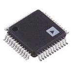
| 供应商器件封装 | 48-LQFP(7x7) |
| 信噪比 | 90 dB |
| 分辨率 | 16 bit |
| 包装 | 托盘 |
| 商标 | Analog Devices |
| 安装类型 | 表面贴装 |
| 安装风格 | SMD/SMT |
| 封装 | Tray |
| 封装/外壳 | 48-LQFP |
| 封装/箱体 | LQFP-48 |
| 工作温度 | -40°C ~ 85°C |
| 工作电源电压 | 5 V |
| 工厂包装数量 | 250 |
| 接口类型 | Parallel, Serial (2-Wire, SPI, QSPI, Microwire) |
| 数据接口 | 串行,并联 |
| 最大功率耗散 | 115 mW |
| 最大工作温度 | + 85 C |
| 最小工作温度 | - 40 C |
| 标准包装 | 1 |
| 特性 | - |
| 电压参考 | External |
| 电压源 | 模拟和数字 |
| 系列 | AD7664 |
| 结构 | SAR |
| 转换器数 | 1 |
| 转换器数量 | 1 |
| 转换速率 | 570 kS/s |
| 输入数和类型 | 2 个伪差分,单极 |
| 输入类型 | Differential |
| 通道数量 | 1 Channel |
| 配用 | /product-detail/zh/EVAL-AD7664CBZ/EVAL-AD7664CBZ-ND/1644950 |
| 采样率(每秒) | 570k |


- 商务部:美国ITC正式对集成电路等产品启动337调查
- 曝三星4nm工艺存在良率问题 高通将骁龙8 Gen1或转产台积电
- 太阳诱电将投资9.5亿元在常州建新厂生产MLCC 预计2023年完工
- 英特尔发布欧洲新工厂建设计划 深化IDM 2.0 战略
- 台积电先进制程称霸业界 有大客户加持明年业绩稳了
- 达到5530亿美元!SIA预计今年全球半导体销售额将创下新高
- 英特尔拟将自动驾驶子公司Mobileye上市 估值或超500亿美元
- 三星加码芯片和SET,合并消费电子和移动部门,撤换高东真等 CEO
- 三星电子宣布重大人事变动 还合并消费电子和移动部门
- 海关总署:前11个月进口集成电路产品价值2.52万亿元 增长14.8%


PDF Datasheet 数据手册内容提取
a 16-Bit, 570 kSPS PulSAR® Unipolar CMOS ADC AD7664 FEATURES FUNCTIONAL BLOCK DIAGRAM Throughput: 570 kSPS (Warp Mode) AVDD AGNDREF REFGND DVDD DGND 500 kSPS (Normal Mode) 444 kSPS (Impulse Mode) AD7664 OVDD INL: (cid:1)2.5 LSB Max ((cid:1)0.0038% of Full Scale) SERIAL OGND IN PORT 16-Bit Resolution with No Missing Codes SWITCHED S/(N+D): 90 dB Typ @ 45 kHz INGND CAP DAC 16 D[15:0] THD: –100 dB Typ @ 45 kHz BUSY PARALLEL Analog Input Voltage Range: 0 V to 2.5 V INTERFACE RD Both AC and DC Specifications CLOCK CS No Pipeline Delay PD Parallel and Serial 5 V/3 V Interface RESET CACLOIBNRTRAOTILO LNO CGIRICC AUNITDRY SER/PAR SPI®/QSPITM/MICROWIRETM/DSP Compatible OB/2C Single 5 V Supply Operation Power Dissipation WARP IMPULSE CNVST 115 mW Maximum, Table I. PulSAR Selection 21 (cid:2)W @ 100 SPS Power-Down Mode: 7 (cid:2)W Max Type/kSPS 100–250 500–570 800–1000 Package: 48-Lead Quad Flat Pack (LQFP) 48-Lead Chip Scale Package (LFCSP) Pseudo AD7651 AD7650/AD7652 AD7653 Pin-to-Pin Compatible Upgrade of the AD7660 Differential AD7660/AD7661 AD7664/AD7666 AD7667 True Bipolar AD7663 AD7665 AD7671 APPLICATIONS Data Acquisition True AD7675 AD7676 AD7677 Instrumentation Differential Digital Signal Processing 18-Bit AD7678 AD7679 AD7674 Spectrum Analysis Medical Instruments Simultaneous/ AD7654 Battery-Powered Systems Multichannel AD7655 Process Control GENERAL DESCRIPTION It is fabricated using Analog Devices’ high performance, 0.6 micron The AD7664 is a 16-bit, 570 kSPS, charge redistribution SAR, CMOS process, with correspondingly low cost and is available in a analog-to-digital converter that operates from a single 5 V power 48-lead LQFP and a tiny 48-lead LFCSP with operation specified supply. The part contains a high speed 16-bit sampling ADC, from –40°C to +85°C. an internal conversion clock, error correction circuits, and both serial and parallel system interface ports. PRODUCT HIGHLIGHTS The AD7664 is hardware factory-calibrated and is comprehensively 1. Fast Throughput tested to ensure such ac parameters as signal-to-noise ratio (SNR) The AD7664 is a 570 kSPS, charge redistribution, 16-bit and total harmonic distortion (THD), in addition to the more SAR ADC with internal error correction circuitry. traditional dc parameters of gain, offset, and linearity. 2. Superior INL It features a very high sampling rate mode (Warp), a fast mode The AD7664 has a maximum integral nonlinearity of 2.5 LSBs (Normal) for asynchronous conversion rate applications, and for with no missing 16-bit code. low power applications, a reduced power mode (Impulse) where 3. Single-Supply Operation the power is scaled with the throughput. The AD7664 operates from a single 5 V supply and dissipates only a maximum of 115mW. In Impulse Mode, its power dissipation decreases with the throughput to, for instance, only 21 µW at a 100 SPS throughput. It consumes 7 µW maximum when in power-down. 4. Serial or Parallel Interface Versatile parallel or 2-wire serial interface arrangement REV. F compatible with both 3 V or 5 V logic. Information furnished by Analog Devices is believed to be accurate and reliable. However, no responsibility is assumed by Analog Devices for its use, nor for any infringements of patents or other rights of third parties that may result from its use. No license is granted by implication or otherwise One Technology Way, P.O. Box 9106, Norwood, MA 02062-9106, U.S.A. under any patent or patent rights of Analog Devices. Trademarks and Tel:781/329-4700 www.analog.com registered trademarks are the property of their respective owners. Fax:781/326-8703 © 2001-2016 Analog Devices, Inc. All rights reserved.
AD7664–SPECIFICATIONS (–40(cid:3)C to +85(cid:3)C, AVDD = DVDD = 5 V, OVDD = 2.7 V to 5.25 V, unless otherwise noted.) Parameter Conditions Min Typ Max Unit RESOLUTION 16 Bits ANALOG INPUT Voltage Range V – V 0 V V IN INGND REF Operating Input Voltage V –0.1 +3 V IN V –0.1 +0.5 V INGND Analog Input CMRR f = 10 kHz 62 dB IN Input Current 570 kSPS Throughput 7 µA Input Impedance See Analog Input Section THROUGHPUT SPEED Complete Cycle In Warp Mode 1.75 µs Throughput Rate In Warp Mode 1 570 kSPS Time between Conversions In Warp Mode 1 ms Complete Cycle In Normal Mode 2 µs Throughput Rate In Normal Mode 0 500 kSPS Complete Cycle In Impulse Mode 2.25 µs Throughput Rate In Impulse Mode 0 444 kSPS DC ACCURACY Integral Linearity Error –2.5 +2.5 LSB1 Differential Linearity Error –1 +1.5 LSB No Missing Codes 16 Bits Transition Noise 0.7 LSB Full-Scale Error2 REF = 2.5 V ±0.08 % of FSR Unipolar Zero Error2 ±5 ±15 LSB Power Supply Sensitivity AVDD = 5 V ±5% ±3 LSB AC ACCURACY Signal-to-Noise f = 100 kHz 90 dB3 IN Spurious-Free Dynamic Range f = 45 kHz 100 dB IN f = 100 kHz 100 dB IN Total Harmonic Distortion f = 45 kHz –100 dB IN f = 100 kHz –100 dB IN Signal-to-(Noise+Distortion) f = 45 kHz 90 dB IN f = 100 kHz 89 dB IN –60 dB Input, f = 100 kHz 30 dB IN –3 dB Input Bandwidth 18 MHz SAMPLING DYNAMICS Aperture Delay 2 ns Aperture Jitter 5 ps rms Transient Response Full-Scale Step 250 ns REFERENCE External Reference Voltage Range 2.3 2.5 AVDD – 1.85 V External Reference Current Drain 570 kSPS Throughput 115 µA DIGITAL INPUTS Logic Levels V –0.3 +0.8 V IL V 2.0 OVDD + 0.3 V IH I –1 +1 µA IL I –1 +1 µA IH DIGITAL OUTPUTS Data Format Parallel or Serial 16-Bits Pipeline Delay Conversion Results Available Immediately after Completed Conversion V I = 1.6 mA 0.4 V OL SINK V I = –500 µA OVDD – 0.6 V OH SOURCE POWER SUPPLIES Specified Performance AVDD 4.75 5 5.25 V DVDD 4.75 5 5.25 V OVDD 2.7 5.25 V Operating Current4 500 kSPS Throughput AVDD 15.5 mA DVDD5 3.8 mA OVDD5 100 µA Power Dissipation5 500 kSPS Throughput4 115 mW 100 SPS Throughput6 21 µW In Power-Down Mode7 7 µW –2– REV. F
AD7664 Parameter Conditions Min Typ Max Unit TEMPERATURE RANGE8 Specified Performance T to T –40 +85 °C MIN MAX NOTES 1LSB means least significant bit. With the 0 V to 2.5 V input range, one LSB is 38.15 µV. 2See Definition of Specifications section. These specifications do not include the error contribution from the external reference. 3All specifications in dB are referred to a full-scale input FS. Tested with an input signal at 0.5 dB below full-scale unless otherwise specified. 4In Normal Mode. 5Tested in Parallel Reading Mode. 6In Impulse Mode. 7With all digital inputs forced to OVDD or OGND, respectively. 8Contact factory for extended temperature range. Specifications subject to change without notice. TIMING SPECIFICATIONS (–40(cid:3)C to +85(cid:3)C, AVDD = DVDD= 5 V, OVDD = 2.7 V to 5.25 V, unless otherwise noted.) Parameter Symbol Min Typ Max Unit REFER TO FIGURES 11 AND 12 Convert Pulse Width t 5 ns 1 Time between Conversions t 1.75/2/2.25 Note 1 µs 2 (Warp Mode/Normal Mode/Impulse Mode) CNVST LOW to BUSY HIGH Delay t 25 ns 3 BUSY HIGH All Modes Except in t 1.5/1.75/2 µs 4 Master Serial Read after Convert Mode (Warp Mode/Normal Mode/Impulse Mode) Aperture Delay t 2 ns 5 End of Conversion to BUSY LOW Delay t 10 ns 6 Conversion Time t 1.5/1.75/2 µs 7 (Warp Mode/Normal Mode/Impulse Mode) Acquisition Time t 250 ns 8 RESET Pulsewidth t 10 ns 9 REFER TO FIGURES 13, 14, AND 15 (Parallel Interface Modes) CNVST LOW to DATA Valid Delay t 1.5/1.75/2 µs 10 (Warp Mode/Normal Mode/Impulse Mode) DATA Valid to BUSY LOW Delay t 45 ns 11 Bus Access Request to DATA Valid t 40 ns 12 Bus Relinquish Time t 5 15 ns 13 REFER TO FIGURES 16 AND 17 (Master Serial Interface Modes)2 CS LOW to SYNC Valid Delay t 10 ns 14 CS LOW to Internal SCLK Valid Delay2 t 10 ns 15 CS LOW to SDOUT Delay t 10 ns 16 CNVST LOW to SYNC Delay t 25/275/525 ns 17 (Warp Mode/Normal Mode/Impulse Mode) SYNC Asserted to SCLK First Edge Delay t 4 ns 18 Internal SCLK Period t 40 75 ns 19 Internal SCLK HIGH (INVSCLK Low)3 t 30 ns 20 Internal SCLK LOW (INVSCLK Low)3 t 9.5 ns 21 SDOUT Valid Setup Time t 4.5 ns 22 SDOUT Valid Hold Time t 3 ns 23 SCLK Last Edge to SYNC Delay t 3 24 CS HIGH to SYNC HI-Z t 10 ns 25 CS HIGH to Internal SCLK HI-Z t 10 ns 26 CS HIGH to SDOUT HI-Z t 10 ns 27 BUSY HIGH in Master Serial Read after Convert t 2.75/3/3.25 µs 28 (Warp Mode/Normal Mode/Impulse Mode) CNVST LOW to SYNC Asserted Delay t 1/1.25/1.5 µs 29 (Warp Mode/Normal Mode/Impulse Mode) SYNC Deasserted to BUSY LOW Delay t 50 ns 30 REFER TO FIGURES 18 AND 20 (Slave Serial Interface Modes)2 External SCLK Setup Time t 5 ns 31 External SCLK Active Edge to SDOUT Delay t 3 16 ns 32 SDIN Setup Time t 5 ns 33 SDIN Hold Time t 5 ns 34 External SCLK Period t 25 ns 35 External SCLK HIGH t 10 ns 36 External SCLK LOW t 10 ns 37 NOTES 1In Warp Mode only, the maximum time between conversions is 1 ms; otherwise, there is no required maximum time. 2In Serial Interface Modes, the SYNC, SCLK, and SDOUT timings are defined with a maximum load C of 10 pF; otherwise, the load is 60 pF maximum. L 3If the polarity of SCLK is inverted, the timing references of SCLK are also inverted. Specifications subject to change without notice. REV. F –3–
AD7664 ABSOLUTE MAXIMUM RATINGS1 IN2, REF, INGND, REFGND to AGND 1.6mA IOL . . . . . . . . . . . . . . . . . . . . . . .AVDD + 0.3V to AGND – 0.3V Ground Voltage Differences TO OUTPUT 1.4V AGND, DGND, OGND . . . . . . . . . . . . . . . . . . . . . . ±0.3 V PIN CL Supply Voltages 60pF* AVDD, DVDD, OVDD . . . . . . . . . . . . . . . . –0.3V to +7 V 500(cid:2)A IOH AVDD to DVDD, AVDD to OVDD . . . . . . . . . . . . . . ±7 V DVDD to OVDD . . . . . . . . . . . . . . . . . . . . . . . . . . . . . ±7 V *IN SERIAL INTERFACE MODES, THE SYNC, SCLK, AND Digital Inputs SDOUT TIMINGS ARE DEFINED WITH A MAXIMUM LOAD Except the Databus D(7:4) . . . . . –0.3 V to DVDD + 3.0 V CL OF 10pF; OTHERWISE, THE LOAD IS 60pF MAXIMUM. Databus D(7:4) . . . . . . . . . . . . . . –0.3 V to OVDD + 3.0 V Figure 1.Load Circuit for Digital Interface Timing, Internal Power Dissipation3 . . . . . . . . . . . . . . . . . . . . 700 mW SDOUT, SYNC, SCLK Outputs, C = 10 pF L Internal Power Dissipation4 . . . . . . . . . . . . . . . . . . . . . . 2.5 W Junction Temperature . . . . . . . . . . . . . . . . . . . . . . . . . . 150°C Storage Temperature Range . . . . . . . . . . . . –65°C to +150°C 2V Lead Temperature Range 0.8V (Soldering 10 sec) . . . . . . . . . . . . . . . . . . . . . . . . . . . 300°C tDELAY tDELAY NOTES 2V 2V 1Stresses above those listed under Absolute Maximum Ratings may cause perma- 0.8V 0.8V nent damage to the device. This is a stress rating only; functional operation of the device at these or any other conditions above those listed in the operational sections Figure 2.Voltage Reference Levels for Timing of this specification is not implied. Exposure to absolute maximum rating condi- tions for extended periods may affect device reliability. 2See Analog Input section. 3Specification is for the device in free air: 48-Lead LQFP; θ = 91°C/W, θ = 30°C/W. JA JC 4Specification is for device in free air: 48-Lead LFCSP; θ = 26°C/W. JA ORDERING GUIDE Temperature Model1 Range Package Description Package Option AD7664ASTZ –40°C to +85°C 48-Lead LQFP ST-48 AD7664ASTZRL –40°C to +85°C 48-Lead LQFP ST-48 AD7664ACPZRL –40°C to +85°C 48-Lead LFCSP CP-48-4 1Z = RoHS Compliant Part. CAUTION ESD (electrostatic discharge) sensitive device. Electrostatic charges as high as 4000V readily WARNING! accumulate on the human body and test equipment and can discharge without detection. Although the AD7664 features proprietary ESD protection circuitry, permanent damage may occur on devices subjected to high energy electrostatic discharges. Therefore, proper ESD precautions are recommended to avoid performance degradation or loss of functionality. ESD SENSITIVE DEVICE –4– REV. F
AD7664 PIN CONFIGURATION D NDGN NCNCNCNCNCINNCNCNCINGREFREF 876543210987 444444444333 AGND 1 36 AGND AVDD 2 35 CNVST NC 3 34 PD DGND 4 33 RESET OB/2C 5 32 CS AD7664 WARP 6 31 RD IMPULSE 7 TOP VIEW 30 DGND SER/PAR 8 (Not to Scale) 29 BUSY D0 9 28 D15 D110 27 D14 D2 11 26 D13 D312 25 D12 345678901234 111111122222 TCKNDDDDTKCR D4/EXT/IND5/INVSYND6/INVSCLD7/RDC/SDIOGNOVDDVDDGND8/SDOUD9/SCLD10/SYN11/RDERRO D NOTES 1. NC = NO CONNECT. DO NOT CONNECTTO THIS PIN. 2. THE EPAD IS CONNECTEDTO GROUND; HOWEVER, THISCONNECTION IS NOT REQUIREDTOMEET SPECIFIED PERFORMANCE. PIN FUNCTION DESCRIPTIONS Pin No. Mnemonic Type Description 1 AGND P Analog Power Ground Pin. 2 AVDD P Input Analog Power Pins. Nominally 5 V. 3, 40–42, NC No Connect. 44–48 4 DGND DI Must Be Tied to the Ground Where DVDD Is Referred. 5 OB/2C DI Straight Binary/Binary Twos Complement. When OB/2C is HIGH, the digital output is straight binary; when LOW, the MSB is inverted resulting in a twos complement output from its internal shift register. 6 WARP DI Mode Selection. When HIGH and IMPULSE LOW, this input selects the fastest mode, the maximum throughput is achievable, and a minimum conversion rate must be applied in order to guarantee full specified accuracy. When LOW, full accuracy is maintained independent of the minimum conversion rate. 7 IMPULSE DI Mode Selection. When HIGH and WARP LOW, this input selects a reduced power mode. In this mode, the power dissipation is approximately proportional to the sampling rate. 8 SER/PAR DI Serial/Parallel Selection Input. When LOW, the Parallel Port is selected; when HIGH, the Serial Interface Mode is selected and some bits of the DATA bus are used as a Serial Port. 9–12 D[0:3] DO Bit 0 to Bit 3 of the Parallel Port Data Output Bus. These pins are always outputs, regardless of the state of SER/PAR. 13 D4 DI/O When SER/PAR is LOW, this output is used as Bit 4 of the Parallel Port Data Output Bus. or EXT/INT When SER/PAR is HIGH, this input, part of the Serial Port, is used as a digital select input for choosing the internal or an external data clock. With EXT/INT tied LOW, the internal clock is selected on the SCLK output. With EXT/INT set to a logic HIGH, output data is synchronized to an external clock signal connected to the SCLK input. 14 D5 DI/O When SER/PAR is LOW, this output is used as Bit 5 of the Parallel Port Data Output Bus. or INVSYNC When SER/PAR is HIGH, this input, part of the Serial Port, is used to select the active state of the SYNC signal. It is active in both Master and Slave Mode. When LOW, SYNC is active HIGH. When HIGH, SYNC is active LOW. 15 D6 DI/O When SER/PAR is LOW, this output is used as Bit 6 of the Parallel Port Data Output Bus. or INVSCLK When SER/PAR is HIGH, this input, part of the Serial Port, is used to invert the SCLK signal. It is active in both Master and Slave Mode. REV. F –5–
AD7664 Pin No. Mnemonic Type Description 16 D7 DI/O When SER/PAR is LOW, this output is used as Bit 7 of the Parallel Port Data Output Bus. or RDC/SDIN When SER/PAR is HIGH, this input, part of the Serial Port, is used as either an external data input or a Read Mode selection input depending on the state of EXT/INT. When EXT/INT is HIGH, RDC/SDIN could be used as a data input to daisy-chain the conversion results from two or more ADCs onto a single SDOUT line. The digital data level on SDIN is output on DATA with a delay of 16 SCLK periods after the initiation of the read sequence. When EXT/INT is LOW, RDC/SDIN is used to select the Read Mode. When RDC/SDIN is HIGH, the data is output on SDOUT during conversion. When RDC/SDIN is LOW, the data can be output on SDOUT only when the conversion is complete. 17 OGND P Input/Output Interface Digital Power Ground. 18 OVDD P Input/Output Interface Digital Power. Nominally at the same supply as the supply of thehost interface (5 V or 3 V). 19 DVDD P Digital Power. Nominally at 5 V. 20 DGND P Digital Power Ground. 21 D8 DO When SER/PAR is LOW, this output is used as Bit 8 of the Parallel Port Data Output Bus. or SDOUT When SER/PAR is HIGH, this output, part of the Serial Port, is used as a serial data output synchronized to SCLK. Conversion results are stored in an on-chip register. The AD7664 provides the conversion result, MSB first, from its internal shift register. The DATA format is determined by the logic level of OB/2C. In Serial Mode, when EXT/INT is LOW, SDOUT is valid on both edges of SCLK. In Serial Mode, when EXT/INT is HIGH: If INVSCLK is LOW, SDOUT is updated on the SCLK rising edge and valid on the next falling edge. If INVSCLK is HIGH, SDOUT is updated on the SCLK falling edge and valid on the next rising edge. 22 D9 DI/O When SER/PAR is LOW, this output is used as Bit 9 of the Parallel Port Data or SCLK Output Bus. When SER/PAR is HIGH, this pin, part of the Serial Port, is used as a serial data clock input or output, dependent upon the logic state of the EXT/INT pin. The active edge where the data SDOUT is updated depends upon the logic state of the INVSCLK pin. 23 D10 DO When SER/PAR is LOW, this output is used as the Bit 10 of the Parallel Port Data Output Bus. or SYNC When SER/PAR is HIGH, this output, part of the Serial Port, is used as a digital output frame synchronization for use with the internal data clock (EXT/INT = Logic LOW). When a read sequence is initiated and INVSYNC is LOW, SYNC is driven HIGH and remains HIGH while the SDOUT output is valid. When a read sequence is initiated and INVSYNC is HIGH, SYNC is driven LOW and remains LOW while the SDOUT output is valid. 24 D11 DO When SER/PAR is LOW, this output is used as Bit 11 of the Parallel Port Data Output Bus. or RDERROR When SER/PAR is HIGH and EXT/INT is HIGH, this output, part of the Serial Port, is used as an incomplete read error flag. In Slave Mode, when a data read is started and not complete when the following conversion is complete, the current data is lost and RDERROR is pulsed HIGH. 25–28 D[12:15] DO Bit 12 to Bit 15 of the Parallel Port Data Output Bus. These pins are always outputs regard- less of the state of SER/PAR. 29 BUSY DO Busy Output. Transitions HIGH when a conversion is started and remains HIGH until the conversion is complete and the data is latched into the on-chip shift register. The falling edge of BUSY could be used as a data-ready clock signal. 30 DGND P Must Be Tied to Digital Ground. 31 RD DI Read Data. When CS and RD are both LOW, the interface parallel or serial output bus is enabled. 32 CS DI Chip Select. When CS and RD are both LOW, the interface parallel or serial output bus is enabled. CS is also used to gate the external clock. 33 RESET DI Reset Input. When set to a logic HIGH, reset the AD7664. Current conversion if any is aborted. If not used, this pin could be tied to DGND. 34 PD DI Power-Down Input. When set to a logic HIGH, power consumption is reduced and conversions are inhibited after the current one is completed. –6– REV. F
AD7664 Pin No. Mnemonic Type Description 35 CNVST DI Start Conversion. A falling edge on CNVST puts the internal sample-and-hold into the hold state and initiates a conversion. In Impulse Mode (IMPULSE HIGH and WARP LOW), if CNVST is held LOW when the acquisition phase (t ) is complete, the internal sample-and-hold is put 8 into the hold state and a conversion is immediately started. 36 AGND P Must Be Tied to Analog Ground. 37 REF AI Reference Input Voltage. 38 REFGND AI Reference Input Analog Ground. 39 INGND AI Analog Input Ground. 43 IN AI Primary Analog Input with a Range of 0 V to V . REF EPAD Exposed Pad. The EPAD is connected to ground; however, this connection is not required to meet specified performance. NOTES AI = Analog Input DI = Digital Input DI/O = Bidirectional Digital DO = Digital Output P = Power DEFINITION OF SPECIFICATIONS Total Harmonic Distortion (THD) THD is the ratio of the rms sum of the first five harmonic Integral Nonlinearity Error (INL) components to the rms value of a full-scale input signal and is Linearity error refers to the deviation of each individual code expressed in decibels. from a line drawn from negative full scale through positive full scale. The point used as negative full scale occurs 1/2 LSB Signal-to-Noise Ratio (SNR) before the first code transition. Positive full scale is defined as a SNR is the ratio of the rms value of the actual input signal to level 1 1/2 LSB beyond the last code transition. The deviation is the rms sum of all other spectral components below the Nyquist measured from the middle of each code to the true straight line. frequency, excluding harmonics and dc. The value for SNR is expressed in decibels. Differential Nonlinearity Error (DNL) In an ideal ADC, code transitions are 1 LSB apart. Differential Signal to (Noise + Distortion) Ratio (S/[N+D]) nonlinearity is the maximum deviation from this ideal value. It is S/(N+D) is the ratio of the rms value of the actual input signal to often specified in terms of resolution for which no missing codes the rms sum of all other spectral components below the Nyquist are guaranteed. frequency, including harmonics but excluding dc. The value for S/(N+D) is expressed in decibels. Full-Scale Error The last transition (from 011...10 to 011...11 in twos Aperture Delay complement coding) should occur for an analog voltage 1 1/2 LSB Aperture delay is a measure of the acquisition performance and below the nominal full scale (2.49994278 V for the 0 V–2.5 V is measured from the falling edge of the CNVST input to when range). The full-scale error is the deviation of the actual level of the input signal is held for a conversion. the last transition from the ideal level. Transient Response Unipolar Zero Error The time required for the AD7664 to achieve its rated accuracy The first transition should occur at a level 1/2 LSB above analog after a full-scale step function is applied to its input. ground (19.073 µV for the 0 V–2.5 V range). Unipolar zero Overvoltage Recovery error is the deviation of the actual transition from that point. The time required for the ADC to recover to full accuracy after Spurious-Free Dynamic Range (SFDR) an analog input signal 150% of full-scale is reduced to 50% of The difference, in decibels (dB), between the rms amplitude of the full-scale value. the input signal and the peak spurious signal. Effective Number of Bits (ENOB) ENOB is a measurement of the resolution with a sine wave input. It is related to S/(N+D) by the following formula: ( [ ] ) ENOB = S N +D −1.76 6.02 dB and is expressed in bits. REV. F –7–
AD7664–Typical Performance Characteristics 2.5 1.50 2.0 1.25 1.5 1.00 1.0 0.75 B 0.5 B0.50 S S NL – L 0 NL – L0.25 I–0.5 D 0 –1.0 –0.25 –1.5 –0.50 –2.0 –0.75 –2.5 –1.00 0 16384 32768 49152 65536 0 16384 32768 49152 65536 CODE CODE TPC 1.Integral Nonlinearity vs. Code TPC 4.Differential Nonlinearity vs. Code 8000 10000 7288 7148 9008 7000 9000 8000 6000 7000 5000 6000 S S T T UN4000 UN5000 O O C C 3000 4000 3340 3643 3000 2000 1173 2000 753 1000 1000 0 0 12 10 0 0 0 0 136 257 0 0 0 0 7F86 7F87 7F88 7F89 7F8A 7F8B 7F8C 7F8D 7F8E 7F8F 7FB3 7FB4 7FB5 7FB6 7FB7 7FB8 7FB9 7FBA 7FBB CODE – Hexa CODE – Hexa TPC 2.Histogram of 16,384 Conversions of a DC Input TPC 5.Histogram of 16,384 Conversions of a DC Input at the Code Transition at the Code Center 140 180 130 170 160 120 150 110 140 100 130 UNITS 9800 UNITS111210000 OF 70 OF 90 BER 60 BER 8700 UM 50 UM 60 N 40 N 50 30 40 30 20 20 10 10 0 0 0 0.5 1.0 1.5 2.0 2.5 –2.5 –2.0 –1.5 –1.0 –0.5 0.0 POSITIVE INL (LSB) NEGATIVE INL (LSB) TPC 3.Typical Positive INL Distribution (600 Units) TPC 6.Typical Negative INL Distribution (600 Units) –8– REV. F
AD7664 0 92 8192 POINT FFT –20 fS = 570kHz dB fIN = 45.5322kHz, –0.5dB – cale) –40 SSNINRA =D 9=0 8.19d.4BdB ALE) SNR dB of Full S ––6800 TSHFDDR = =– 9977..15ddBB O FULL SC90 S/(N+D) UDE (–100 RED T LIT–120 ER88 P F M E A–140 R R ( N –160 S –180 86 0 57 114 171 228 285 –60 –50 –40 –30 –20 –10 0 FREQUENCY (kHz) INPUT LEVEL – dB TPC 7.FFT Plot TPC 10.SNR and S/(N+D) vs. Input Level (Referred to Full Scale) 100 16.0 96 –96 95 15.5 93 –98 SNR AND S/[N+D] – dB 988005 SSEN/N(NRO+BD) 111544...005 ENOB – Bits SNR AND S/(N+D) – dB90 STNHRD –100 THD – dB 87 –102 75 13.5 70 13.0 84 –104 1 10 100 1000 –55 –35 –15 5 25 45 65 85 105 125 FREQUENCY – kHz TEMPERATURE – (cid:3)C TPC 8.SNR, S/(N+D), and ENOB vs. Frequency TPC 11.SNR, S/(N+D), THD vs. Temperature –60 110 100k AVDD, WARP/NORMAL –65 105 10k –70 SFDR 100 (cid:2)A 1k DVDD, WARP/NORMAL dB –75 95 S – MONIC – ––8805 9805 R – dB URRENT 10100 DVDD,A IVMDPDU,L ISMEPULSE HAR –90 80 SFD NG C THD, –95 SECOND HARMONIC THD 75 PERATI 0.11 OVDD, ALL MODES –100 70 O –105 65 0.01 THIRD HARMONIC –110 60 0.001 1 10 100 1000 0.1 1 10 100 1k 10k 100k 1M FREQUENCY – kHz SAMPLING RATE – SPS TPC 9. THD, Harmonics, and SFDR vs. Frequency TPC 12.Operating Currents vs. Sample Rate REV. F –9–
AD7664 10 100 A R (LSB) 68 FULL-SCALE ERROR NTS – n 8900 CALE ERRO 24 ZERO ERROR TING CURRE 657000 DVDD S 0 A ROR, FULL- ––42 OWN OPER 432000 R D O E –6 ER- 10 AVDD R W ZE –8 PO 0 OVDD –10 –10 –55 –35 –15 5 25 45 65 85 105 125 –40 –15 10 35 60 85 TEMPERATURE ((cid:3)C) TEMPERATURE – (cid:3)C TPC 13.Zero Error, Full-Scale Error vs. Temperature TPC 15.Power-Down Operating Currents vs. Temperature 50 OVDD = 2.7V, 85(cid:3)C 40 s – n30 AY OVDD = 2.7V, 25(cid:3)C L E D t 1220 OVDD = 5V, 85(cid:3)C 10 OVDD = 5V, 25(cid:3)C 0 0 50 100 150 200 CL – pF TPC 14.Typical Delay vs. Load Capacitance C L –10– REV. F
AD7664 CIRCUIT INFORMATION input IN. Thus, the capacitor array is used as a sampling capacitor The AD7664 is a very fast, low power, single-supply, precise and acquires the analog signal on the IN input. Similarly, the 16-bit analog-to-digital converter (ADC). The AD7664 features dummy capacitor acquires the analog signal on the INGND input. different modes to optimize performances according to the When the CNVST input goes LOW, a conversion phase is applications. initiated. When the conversion phase begins, SW and SW A B In Warp Mode, the AD7664 is capable of converting 570,000 are opened first. The capacitor array and the dummy capacitor samples per second (570 kSPS). are then disconnected from the inputs and connected to the REFGND input. Therefore, the differential voltage between IN The AD7664 provides the user with an on-chip track-and-hold, and INGND captured at the end of the acquisition phase is successive-approximation ADC that does not exhibit any pipeline applied to the comparator inputs, causing the comparator to or latency, making it ideal for multiple multiplexed channel become unbalanced. By switching each element of the capacitor applications. array between REFGND or REF, the comparator input varies by The AD7664 can be operated from a single 5 V supply and binary-weighted voltage steps (V /2, V /4,...V /65536). REF REF REF interfaced to either 5 V or 3 V digital logic. It is housed in a The control logic toggles these switches, starting with the MSB 48-lead LQFP package or a 48-lead LFCSP package that first, to bring the comparator back into a balanced condition. After saves space and allows flexible configurations as either a the completion of this process, the control logic generates the serial or parallel interface. The AD7664 is a pin-to-pin com- ADC output code and brings BUSY output LOW. patible upgrade of the AD7660. Modes of Operation The AD7664 features three modes of operation: Warp, Nor- CONVERTER OPERATION mal, and Impulse. Each of these modes is suitable for specific The AD7664 is a successive-approximation analog-to-digital applications. converter based on a charge redistribution DAC. Figure 3 shows the simplified schematic of the ADC. The capacitive The Warp Mode allows the fastest conversion rate up to 570 kSPS. DAC consists of an array of 16 binary weighted capacitors However, in this mode and this mode only, the full specified accuracy and an additional LSB capacitor. The comparator’s negative is guaranteed only when the time between conversions does not input is connected to a dummy capacitor of the same value as exceed 1 ms. If the time between two consecutive conversions is the capacitive DAC array. longer than 1 ms, for instance, after power-up, the first conversion result should be ignored. This mode makes the AD7664 ideal During the acquisition phase, the common terminal of the array for applications where both high accuracy and fast sample rate tied to the comparator’s positive input is connected to AGND are required. via SW . All independent switches are connected to the analog A IN REF REFGND SWITCHES CONTROL MSB LSB SWA 32,768C 16,384C 4C 2C C C BUSY CONTROL COMP LOGIC INGND OUTPUT 65,536C CODE SWB CNVST Figure 3.ADC Simplified Schematic REV. F –11–
AD7664 The Normal Mode is the fastest mode (500 kSPS) without any Table II. Output Codes and Ideal Input Voltages limitation on the time between conversions. This mode makes the AD7664 ideal for asynchronous applications such as data Digital Output Code acquisition systems, where both high accuracy and fast sample Hexa rate are required. Analog Straight Twos Description Input Binary Complement The Impulse Mode, the lowest power dissipation mode, allows power saving between conversions. When operating at 100 SPS, FSR – 1 LSB 2.499962 V FFFF1 7FFF1 for example, it typically consumes only 21 µW. This feature FSR – 2 LSB 2.499923 V FFFE 7FFE makes the AD7664 ideal for battery-powered applications. Midscale + 1 LSB 1.250038 V 8001 0001 Midscale 1.25 V 8000 0000 Transfer Functions Midscale – 1 LSB 1.249962 V 7FFF FFFF Using the OB/2C digital input, the AD7664 offers two output –FSR + 1 LSB 38 µV 0001 8001 codings: straight binary and twos complement. The LSB size is –FSR 0 V 00002 80002 V /65536, which is about 38.15 µV. The ideal transfer charac- REF teristics for the AD7664 are shown in Figure 4 and Table II. NOTES 1This is also the code for overrange analog input (V – V above IN INGND V – V ). REF REFGND 2This is also the code for underrange analog input (V below V ). IN INGND 1 LSB = VREF/65536 TYPICAL CONNECTION DIAGRAM 111...111 y Figure 5 shows a typical connection diagram for the AD7664. ar 111...110 n Bi 111...101 ht g ai Str – E D O C C D A 000...010 000...001 000...000 00.5V LSB 1 LSB VREF – 1 LSB VREF – 1.5 LSB ANALOG INPUT Figure 4.ADC Ideal Transfer Function ANALOG 100(cid:4) DIGITAL SUPPLY SUPPLY (3.3V OR 5V) (5V) 10(cid:2)F 100nF 10(cid:2)F 100nF 100nF 10(cid:2)F AVDD AGND DGND DVDD OVDD OGND SERIAL PORT SCLK 2.5V REF1 REF SDOUT CREF1 1(cid:2)F REFGND BUSY (cid:2)C/(cid:2)P/DSP AD7664 CNVST D3 15(cid:4) U12 IN ANALOG INPUT OB/2C (0V TO 2.5V) SER/PAR DVDD CC 4.7nF WARP INGND IMPULSE PD RESET CS RD CLOCK NOTES 1THE ADR421 IS RECOMMENDED WITH CREF = 47(cid:2)F. 2THE AD8021 IS RECOMMENDED WITH A COMPENSATION CAPACITOR CC = 10 pF, TYPE CERAMIC NPO. 3OPTIONAL LOW JITTER CNVST. Figure 5.Typical Connection Diagram –12– REV. F
AD7664 Analog Input significantly affect the ac performances, especially the total Figure 6 shows an equivalent circuit of the input structure of harmonic distortion (THD). The maximum source impedance the AD7664. depends on the amount of THD that can be tolerated. The THD degrades in function of the source impedance and the AVDD maximum input frequency as shown in Figure 8. –70 D1 R1 C2 IN OR INGND C1 R = 50(cid:4) D2 –75 AGND –80 The two dFiiogduerse D6.1 Eaqnudi vDa2le pnrto Avindael oEgS DIn ppurot tCecirtciounit for the HD – dB –85 R = 100(cid:4) R = 11(cid:4) T analog inputs IN and INGND. Care must be taken to ensure –90 that the analog input signal never exceeds the supply rails by more than 0.3 V. This will cause these diodes to become forward- biased and start conducting current. These diodes can handle –95 a forward-biased current of 100 mA maximum. For instance, these conditions could eventually occur when the input buffer’s –100 10 100 1000 (U1) supplies are different from AVDD. In such cases, an input FREQUENCY – kHz buffer with a short circuit current limitation can be used to Figure 8.THD vs. Analog Input Frequency and protect the part. Source Resistance This analog input structure allows the sampling of the differen- Driver Amplifier Choice tial signal between IN and INGND. Unlike other converters, Although the AD7664 is easy to drive, the driver amplifier needs the INGND input is sampled at the same time as the IN input. to meet at least the following requirements: By using this differential input, small signals common to both inputs are rejected, as shown in Figure 7, which represents the • The driver amplifier and the AD7664 analog input circuit typical CMRR over frequency. For instance, by using INGND must be able, together, to settle for a full-scale step of the to sense a remote signal ground, difference of ground potentials capacitor array at a 16-bit level (0.0015%). In the amplifier’s between the sensor and the local ADC ground are eliminated. data sheet, the settling at 0.1% to 0.01% is more commonly specified. It could significantly differ from the settling time at 70 16-bit level and it should, therefore, be verified prior to the driver selection. The tiny op amp AD8021, which combines 60 ultralow noise and a high gain bandwidth, meets this settling time requirement even when used with high gain up to 13. 50 • The noise generated by the driver amplifier needs to be kept as B low as possible in order to preserve the SNR and transition – d 40 noise performance of the AD7664. The noise coming from R MR 30 the driver is filtered by the AD7664 analog input circuit one- C pole low-pass filter made by R1 and C2 or the external filter, if 20 any is used. The SNR degradation due to the amplifier is: 10 0 1k 10k 100k 1M 28 FREQUENCY – Hz SNR =20log Figure 7.Analog Input CMRR vs. Frequency LOSS 784+ π f (Ne )2 2 –3dB N During the acquisition phase, the impedance of the analog input IN can be modeled as a parallel combination of capacitor C1 and the network formed by the series connection of R1 and C2. where: Capacitor C1 is primarily the pin capacitance. The resistor R1 is typically 140 Ω and is a lumped component made up of some f is the –3 dB input bandwidth in MHz of the AD7664 –3 dB serial resistors and the on resistance of the switches. The capacitor (18 MHz) or the cutoff frequency of the input filter, if C2 is typically 60 pF and is mainly the ADC sampling capacitor. any used. During the conversion phase, where the switches are opened, the input N is the noise gain of the amplifier (1, if in buffer impedance is limited to C1. The R1, C2 makes a one-pole low-pass configuration). filter that reduces the undesirable aliasing effect and limits the noise. e is the equivalent input noise voltage of the op amp in When the source impedance of the driving circuit is low, the N nV/√Hz. AD7664 can be driven directly. Large source impedances will REV. F –13–
AD7664 For instance, in a driver like the AD8021, with an equivalent (DVDD) can be supplied through a simple RC filter from the input noise of 2 nV/√Hz and configured as a buffer, thus with a analog supply as shown in Figure 5. The AD7664 is independent noise gain of 1, the SNR degrades by 0.58 dB. of power supply sequencing and thus free from supply voltage • The driver needs to have a THD performance suitable to that induced latch-up. Additionally, it is very insensitive to power supply variations over a wide frequency range, as shown in Figure 9. of the AD7664. TPC 12 gives the THD versus frequency that the driver should preferably exceed. POWER DISSIPATION VERSUS THROUGHPUT The AD8021 meets these requirements and is usually appropri- Operating currents are very low during the acquisition phase, which ate for almost all applications. The AD8021 needs an external allows significant power savings when the conversion rate is compensation capacitor of 10 pF. This capacitor should have reduced, as shown in Figure 10. This power saving depends on the good linearity as an NPO ceramic or mica type. mode used. In Impulse Mode, the AD7664 automatically reduces The AD8022 could also be used where a dual version is needed its power consumption at the end of each conversion phase. This and a gain of 1 is used. feature makes the AD7664 ideal for very low power battery- operated applications. It should be noted that the digital interface The AD829 is another alternative where high frequency (above remains active even during the acquisition phase. To reduce the 100 kHz) performance is not required. In a gain of 1, it requires operating digital supply currents even further, the digital inputs an 82 pF compensation capacitor. need to be driven close to the power supply rails (i.e., DVDD or The AD8610 is another option where low bias current is needed DGND for all inputs except EXT/INT, INVSYNC, INVSCLK, in low frequency applications. RDC/SDIN, and OVDD or OGND for these last four inputs). Voltage Reference Input The AD7664 uses an external 2.5 V voltage reference. –50 The voltage reference input REF of the AD7664 has a dynamic input impedance; it should, therefore, be driven by a low imped- –55 ance source with an efficient decoupling between REF and REFGND inputs. This decoupling depends on the choice of the –60 voltage reference, but usually consists of a 1 µF ceramic capacitor B d and a low ESR tantalum capacitor connected to the REF and R – –65 REFGND inputs with minimum parasitic inductance. 47 µF is an SR P appropriate value for the tantalum capacitor when used with one –70 of the recommended reference voltages: • The low noise, low temperature drift ADR421 and AD780 –75 voltage references • The low power ADR291 voltage reference –80 1 10 100 1000 • The low cost AD1582 voltage reference INPUT FREQUENCY – kHz For applications using multiple AD7664s, it is more effective to Figure 9.PSRR vs. Frequency buffer the reference voltage with a low noise, very stable op amp like the AD8031. 100k WARP/NORMAL Care should also be taken with the reference temperature coeffi- cient of the voltage reference that directly affects the full-scale 10k accuracy, if this parameter matters. For instance, a ±15 ppm/°C W (cid:2) tempco of the reference changes the full scale by ±1 LSB/°C. N – 1k O V , as mentioned in the specification table, could be increased to TI REF A AVDD – 1.85 V. The benefit here is the increased SNR obtained SIP 100 S IMPULSE as a result of this increase. Since the input range is defined in DI R terms of V , this would essentially increase the range to make it E 10 REF W a 0 V to 3 V input range with an AVDD above 4.85 V. The O P theoretical improvement as a result of this increase in reference is 1 1.58 dB (20 log [3/2.5]). Due to the theoretical quantization noise, however, the observed improvement is approximately 1 dB. The 0.1 AD780 can be selected with a 3 V reference voltage. 0.1 1 10 100 1k 10k 100k 1M SAMPLING RATE – SPS Power Supply Figure 10.Power Dissipation vs. Sample Rate The AD7664 uses three sets of power supply pins: an analog 5 V supply AVDD, a digital 5 V core supply DVDD, and a digital input/output interface supply OVDD. The OVDD supply allows direct interface with any logic working between 2.7 V and 5.25 V. To reduce the number of supplies needed, the digital core –14– REV. F
AD7664 CONVERSION CONTROL DIGITAL INTERFACE Figure 11 shows the detailed timing diagrams of the conversion The AD7664 has a versatile digital interface; it can be interfaced process. The AD7664 is controlled by the signal CNVST, which with the host system by using either a serial or parallel interface. initiates conversion. Once initiated, it cannot be restarted or The serial interface is multiplexed on the parallel databus. The aborted, even by the power-down input PD, until the conver- AD7664 digital interface also accommodates both 3 V or 5 V logic sion is complete. The CNVST signal operates independently of by simply connecting the OVDD supply pin of the AD7664 to CS and RD signals. the host system interface digital supply. Finally, by using the OB/2C input pin, either twos complement or straight binary t2 coding can be used. t 1 The two signals CS and RD control the interface. CS and RD CNVST have a similar effect, because they are OR’d together internally. When at least one of these signals is HIGH, the interface out- puts are in high impedance. Usually, CS allows the selection of each AD7664 in multicircuit applications and is held LOW in a BUSY t single AD7664 design. RD is generally used to enable the con- 4 t3 t version result on the databus. 6 t 5 CS = RD = 0 MODE ACQUIRE CONVERT ACQUIRE CONVERT t 1 t t 7 8 CNVST Figure 11.Basic Conversion Timing t In Impulse Mode, conversions can be automatically initiated. If 10 CNVST is held LOW when BUSY is LOW, the AD7664 controls BUSY t 4 the acquisition phase and then automatically initiates a new t 3 t conversion. By keeping CNVST LOW, the AD7664 keeps the 11 conversion process running by itself. It should be noted that the DATA BUS PREVIOUS CONVERSION DATA NEW DATA analog input has to be settled when BUSY goes LOW. Also, at power-up, CNVST should be brought LOW once to initiate the Figure 13.Master Parallel Data Timing for Reading conversion process. In this mode, the AD7664 could sometimes (Continuous Read) run slightly faster then the guaranteed limits in the Impulse Mode of 444 kSPS. This feature does not exist in Warp or PARALLEL INTERFACE Normal Modes. The AD7664 is configured to use the parallel interface when the SER/PAR is held LOW. The data can be read either after t 9 each conversion, which is during the next acquisition phase, RESET or during the following conversion as shown, respectively, in Figures 14 and 15. When the data is read during the conversion, however, it is recommended that it be read-only during the first half of the conversion phase. This avoids any potential feed- BUSY through between voltage transients on the digital interface and the most critical analog conversion circuitry. DATABUS CS t 8 CNVST RD Figure 12.RESET Timing Although CNVST is a digital signal, it should be designed with BUSY special care with fast, clean edges, and levels with minimum overshoot and undershoot or ringing. It is a good thing to shield the CNVST trace with ground and DATABUS CURRENT also to add a low value serial resistor (i.e., 50 Ω) termination CONVERSION close to the output of the component that drives this line. t12 t13 For applications where the SNR is critical, the CNVST signal Figure 14.Slave Parallel Data Timing for Reading should have a very low jitter. This may be achieved by using a (Read after Convert) dedicated oscillator for CNVST generation or, at least, to clock it with a high frequency, low jitter clock as shown in Figure 5. REV. F –15–
AD7664 SERIAL INTERFACE CS = 0 t The AD7664 is configured to use the serial interface when the 1 CNVST, SER/PAR is held HIGH. The AD7664 outputs 16 bits of data, RD MSB first, on the SDOUT pin. This data is synchronized with the 16 clock pulses provided on the SCLK pin. The output data is valid on both the rising and falling edge of the data clock. BUSY t 4 MASTER SERIAL INTERFACE t 3 Internal Clock The AD7664 is configured to generate and provide the serial data DATABUS PREVIOUS clock SCLK when the EXT/INT pin is held LOW. The AD7664 CONVERSION also generates a SYNC signal to indicate to the host when the t12 t13 serial data is valid. The serial clock SCLK and the SYNC signal Figure 15.Slave Parallel Data Timing for Reading can be inverted, if desired. Depending on RDC/SDIN input, (Read during Convert) the data can be read after each conversion or during the fol- lowing conversion. Figures 16 and 17 show the detailed timing diagrams of these two modes. EXT/INT = 0 RDC/SDIN = 0 INVSCLK = INVSYNC = 0 CS, RD t 3 CNVST BUSY t28 t 30 t 29 t 25 SYNC t t 14 18 t 19 t20 t21 t24 t 26 SCLK 1 2 3 14 15 16 t 15 t 27 SDOUT X D15 D14 D2 D1 D0 t t 16 t 23 22 Figure 16.Master Serial Data Timing for Reading (Read after Convert) EXT/INT = 0 RDC/SDIN = 1 INVSCLK = INVSYNC = 0 CS, RD t 1 CNVST t 3 BUSY t 17 t 25 SYNC t t 14 19 t t 20 21 t 24 t t 26 SCLK 15 1 2 3 14 15 16 t 18 t 27 SDOUT X D15 D14 D2 D1 D0 t t 16 t 23 22 Figure 17.Master Serial Data Timing for Reading (Read Previous Conversion during Convert) –16– REV. F
AD7664 CS EXT/INT = 1 INVSCLK = 0 RD = 0 BUSY t 35 t t 36 37 SCLK 1 2 3 14 15 16 17 18 t31 t32 SDOUT X D15 D14 D13 D1 D0 X15 X14 t16 t34 SDIN X15 X14 X13 X1 X0 Y15 Y14 t 33 Figure 18.Slave Serial Data Timing for Reading (Read after Convert) Because the AD7664 is used with a fast throughput, the Mas- while both CS and RD are LOW. The data is shifted out, ter Read During Conversion Mode is the most often recom- MSB first, with 16 clock pulses and is valid on both the rising mended Serial Mode, when it can be used. In this mode, the and falling edge of the clock. serial clock and data toggle at appropriate instants that mini- Among the advantages of this method, the conversion perfor- mize potential feedthrough between digital activity and the mance is not degraded, because there are no voltage tran- critical conversion decisions. sients on the digital interface during the conversion process. In Read-after-Conversion Mode, it should be noted that, unlike Another advantage is the ability to read the data at any speed up to in other modes, the signal BUSY returns LOW after the 16 data 40 MHz, which accommodates both slow digital host interface bits are pulsed out and not at the end of the conversion phase, and the fastest serial reading. which results in a longer BUSY width. Finally, in this mode only, the AD7664 provides a daisy-chain SLAVE SERIAL INTERFACE feature using the RDC/SDIN input pin for cascading multiple External Clock converters together. This feature is useful for reducing component The AD7664 is configured to accept an externally supplied count and wiring connections when desired as, for instance, in serial data clock on the SCLK pin when the EXT/INT pin is isolated multiconverter applications. held HIGH. In this mode, several methods can be used to read An example of the concatenation of two devices is shown in the data. The external serial clock is gated by CS. When CS and Figure 19. Simultaneous sampling is possible by using a com- RD are both LOW, the data can be read after each conversion mon CNVST signal. It should be noted that the RDC/SDIN or during the following conversion. The external clock can be input is latched on the edge of SCLK opposite to the one used either a continuous or discontinuous clock. A discontinuous to shift out the data on SDOUT. Therefore, the MSB of the clock can be either normally HIGH or normally LOW, when upstream converter just follows the LSB of the downstream inactive. Figures 18 and 20 show the detailed timing diagrams of converter on the next SCLK cycle. these methods. While the AD7664 is performing a bit decision, it is important BUSY OUT that voltage transients not occur on digital input/output pins or degradation of the conversion result could occur. This is par- BUSY BUSY ticularly important during the second half of the conversion AD7664 AD7664 phase, because the AD7664 provides error correction circuitry #2 #1 that can correct for an improper bit decision made during the (UPSTREAM) (DOWNSTREAM) first half of the conversion phase. For this reason, it is recom- RDC/SDIN SDOUT RDC/SDIN SDOUT DATA OUT mended that when an external clock is being provided, it is a CNVST CNVST discontinuous clock that is toggling only when BUSY is LOW or, more importantly, that it does not transition during the latter CS CS half of BUSY HIGH. SCLK SCLK External Discontinuous Clock Data Read after Conversion Though the maximum throughput cannot be achieved using this SCLK IN mode, it is the most often recommended of the serial Slave CS IN CNVST IN Modes. Figure 18 shows the detailed timing diagrams of this method. After a conversion is complete, indicated by BUSY Figure 19.Two AD7664s in a Daisy-Chain Configuration returning LOW, the result of this conversion can be read REV. F –17–
AD7664 EXT/INT = 1 INVSCLK = 0 RD = 0 CS CNVST BUSY t3 t35 t t 36 37 SCLK 1 2 3 14 15 16 t 31 t 32 SDOUT X D15 D14 D13 D1 D0 t 16 Figure 20.Slave Serial Data Timing for Reading (Read Previous Conversion during Convert) External Clock Data Read during Conversion SPI Interface (ADSP-219x) Figure 20 shows the detailed timing diagram of this method. Figure 21 shows an interface diagram between the AD7664 and During a conversion, while both CS and RD are LOW, the result an SPI-equipped ADSP-219x. To accommodate the slower speed of the previous conversion can be read. The data is shifted out of the DSP, the AD7664 acts as a slave device and data must be MSB first with 16 clock pulses, and is valid on both the rising and read after conversion. This mode also allows the daisy-chain falling edge of the clock. The 16 bits have to be read before the feature. The convert command can be initiated in response to current conversion is complete; otherwise, RDERROR is pulsed an internal timer interrupt. The reading process can be initi- HIGH and can be used to interrupt the host interface to ated in response to the end-of-conversion signal (BUSY going prevent incomplete data reading. There is no daisy-chain LOW) using an interrupt line of the DSP. The serial interface feature in this mode and RDC/SDIN input should always be tied (SPI) on the ADSP-219x is configured for master mode— either HIGH or LOW. (MSTR) = 1, Clock Polarity bit (CPOL) = 0, Clock Phase bit (CPHA) = 1, and SPI Interrupt Enable (TIMOD) = 00— by To reduce performance degradation due to digital activity, a fast writing to the SPI control register (SPICLTx). To meet all discontinuous clock of at least 18 MHz when in Impulse Mode, timing requirements, the SPI clock should be limited to 17 25 MHz when in Normal Mode, or 40 MHz when in Warp Mbps, which allows it to read an ADC result in less than 1 µs. Mode is recommended to ensure that all the bits are read during When a higher sampling rate is desired, use of one of the the first half of the conversion phase. It is also possible to begin parallel interface modes is recommended. to read the data after conversion and continue to read the last bits even after a new conversion has been initiated. That allows the use of a slower clock speed such as 14 MHz in Impulse Mode, 18 MHz DVDD AD7664* ADSP-219x* in Normal Mode, and 25 MHz in Warp Mode. SER/PAR MICROPROCESSOR INTERFACING EXT/INT The AD7664 is ideally suited for traditional dc measurement BUSY PFx applications supporting a microprocessor and ac signal processing CS SPIxSEL (PFx) applications interfacing to a digital signal processor. The AD7664 RD SDOUT MISOx is designed to interface either with a parallel 8-bit or 16-bit wide INVSCLK SCLK SCKx interface, or with a general-purpose serial port or I/O ports on CNVST PFx or TFSx a microcontroller. A variety of external buffers can be used *ADDITIONAL PINS OMITTED FOR CLARITY with the AD7664 to prevent digital noise from coupling into the Figure 21.Interfacing the AD7664 to an SPI Interface ADC. The following section discusses the use of an AD7664 with an ADSP-219x SPI equipped DSP. –18– REV. F
AD7664 APPLICATION HINTS It is recommended to avoid running digital lines under the Bipolar and Wider Input Ranges device, because these couple noise onto the die. The analog In some applications, it is desired to use a bipolar or wider ana- ground plane should be allowed to run under the AD7664 to avoid log input range like, for instance, ±10 V, ±5 V, or 0 V to 5 V. noise coupling. Fast switching signals like CNVST or clocks Although the AD7664 has only one unipolar range, by simple should be shielded with digital ground to avoid radiating modifications of the input driver circuitry, bipolar and wider noise to other sections of the board and should never run input ranges can be used without any performance degradation. near analog signal paths. Crossover of digital and analog signals should be avoided. Traces on different but close layers of the Figure 22 shows a connection diagram that allows this. board should run at right angles to each other. This reduces the Component values required and resulting full-scale ranges are effect of feedthrough through the board. shown in Table III. The power supplies’ lines to the AD7664 should use as large a For applications where accurate gain and offset are desired, they trace as possible to provide low impedance paths and reduce the can be calibrated by acquiring a ground and a voltage reference effect of glitches on the power supplies’ lines. Good decoupling using an analog multiplexer, U2, as shown for bipolar input is also important to lower the supplies’ impedance presented to ranges in Figure 22. the AD7664 and to reduce the magnitude of the supply spikes. Decoupling ceramic capacitors, typically 100 nF, should be R1 placed on each power supply’s pins AVDD, DVDD, and OVDD ANALOG R2 close to, and ideally right up against, these pins and their corre- INPUT 5(cid:4) sponding ground pins. Additionally, low ESR 10 µF capacitors U1 IN 10nF should be located in the vicinity of the ADC to further reduce low AD7664 frequency ripple. U2 R3 R4 100nF The DVDD supply of the AD7664 can be either a separate supply or come from the analog supply AVDD or the digital interface INGND supply OVDD. When the system digital supply is noisy, or fast 2.5V REF REF switching digital signals are present, it is recommended that, if no CREF 1(cid:2)F separate supply is available, to connect the DVDD digital supply to the analog supply, AVDD, through an RC filter, as shown REFGND in Figure 5, and to connect the system supply to the interface digital supply, OVDD, and the remaining digital circuitry. When Figure 22.Using the AD7664 in 16-Bit Bipolar and/or DVDD is powered from the system supply, it is useful to insert Wider Input Ranges a bead to further reduce high frequency spikes. Table III. Component Values and Input Ranges The AD7664 has five different ground pins: INGND, REFGND, AGND, DGND, and OGND. INGND is used to sense the Input Range R1 (k(cid:4)) R2 (k(cid:4)) R3 (k(cid:4)) R4 (k(cid:4)) analog input signal. REFGND senses the reference, voltage and ±10 V 1 8 10 8 should be a low impedance return to the reference because it ±5 V 1 4 10 6.67 carries pulsed currents. AGND is the ground to which most internal ADC analog signals are referenced. This ground must 0 V to –5 V 1 2 None 0 be connected with the least resistance to the analog ground Layout plane. DGND must be tied to the analog or digital ground The AD7664 has very good immunity to noise on the power plane, depending on the configuration. OGND is connected to supplies, as can be seen in Figure 9. However, care should still the digital system ground. be taken with regard to grounding layout. The printed circuit board that houses the AD7664 should be designed so that the analog and digital sections are separated and confined to certain areas of the board. This facilitates the use of ground planes that can be easily separated. Digital and analog ground planes should be joined in only one place, preferably underneath the AD7664, or, at least, as close as possible to the AD7664. If the AD7664 is in a system where multiple devices require analog-to-digital ground connections, the connection should still be made at one point only, a star ground point that should be established as close as possible to the AD7664. REV. F –19–
AD7664 OUTLINE DIMENSIONS 9.20 0.75 9.00 SQ 1.60 0.60 MAX 8.80 0.45 48 37 1 36 PIN 1 7.20 1.45 TOP VIEW 7.00 SQ 1.40 0.20 (PINS DOWN) 6.80 0.09 1.35 7° 3.5° 12 25 0.15 0° 13 24 0.05 SPLEAANTEING 0C.O08PLANARITY VIEW A 0.50 0.27 BSC 0.22 LEAD PITCH 0.17 VIEW A ROTATED 90° CCW COMPLIANTTO JEDEC STANDARDS MS-026-BBC 051706-A Figure 40. 48-Lead Plastic Quad Flat Package [LQFP] (ST-48) Dimensions shown in millimeters 7.00 0.30 BSC SQ 0.23 PIN 1 0.18 PIN 1 INDICATOR INDICATOR 37 48 36 1 0.50 BSC EXPOSED 5.20 PAD 5.10 SQ 5.00 25 12 24 13 0.45 0.25 MIN TOP VIEW BOTTOM VIEW 0.40 0.35 FOR PROPER CONNECTION OF 0.80 THE EXPOSED PAD, REFER TO 0.75 THE PIN CONFIGURATION AND 0.05 MAX FUNCTION DESCRIPTIONS 0.70 0.02 NOM SECTION OF THIS DATA SHEET. COPLANARITY 0.08 SEATING 0.20 REF PLANE B COMPLIANT TO JEDEC STANDARDS MO-220-WKKD. 112408- Figure 41. 48-Lead Lead Frame Chip Scale Package [LFCSP] 7 x 7 mm Body and 0.75 mm Package Height (CP-48-4) Dimensions shown in millimeters –20– REV. F
AD7664 Revision History Location Page 2/16—REV. E to REV. F. Changes to ORDERING GUIDE . . . . . . . . . . . . . . . . . . . . . . . . . . . . . . . . . . . . . . . . . . . . . . . . . . . . . . . . . . . . . . . . . . . . . . . . . . .4 Changes to PIN CONFIGURATION . . . . . . . . . . . . . . . . . . . . . . . . . . . . . . . . . . . . . . . . . . . . . . . . . . . . . . . . . . . . . . . . . . . . . . . . . 5 Changes to PIN FUNCTION DESCRIPTIONS . . . . . . . . . . . . . . . . . . . . . . . . . . . . . . . . . . . . . . . . . . . . . . . . . . . . . . . . . . . . . . . . . . 7 Deleted Evaluating the AD7664 Performance Section . . . . . . . . . . . . . . . . . . . . . . . . . . . . . . . . . . . . . . . . . . . . . . . . . . . . . . . . . . . . . . . 19 Updated OUTLINE DIMENSIONS . . . . . . . . . . . . . . . . . . . . . . . . . . . . . . . . . . . . . . . . . . . . . . . . . . . . . . . . . . . . . . . . . . . . . . . 20 1/04—Data Sheet changed from REV. D to REV. E. Changes to title . . . . . . . . . . . . . . . . . . . . . . . . . . . . . . . . . . . . . . . . . . . . . . . . . . . . . . . . . . . . . . . . . . . . . . . . . . . . . . . . . . . . . . . . .1 Changes to FEATURES . . . . . . . . . . . . . . . . . . . . . . . . . . . . . . . . . . . . . . . . . . . . . . . . . . . . . . . . . . . . . . . . . . . . . . . . . . . . . . . . . .1 10/03—Data Sheet changed from REV. C to REV. D. Changes to title . . . . . . . . . . . . . . . . . . . . . . . . . . . . . . . . . . . . . . . . . . . . . . . . . . . . . . . . . . . . . . . . . . . . . . . . . . . . . . . . . . . . . . . . .1 Added PulSAR Selection table . . . . . . . . . . . . . . . . . . . . . . . . . . . . . . . . . . . . . . . . . . . . . . . . . . . . . . . . . . . . . . . . . . . . . . . . . . . . .1 Changes to FEATURES . . . . . . . . . . . . . . . . . . . . . . . . . . . . . . . . . . . . . . . . . . . . . . . . . . . . . . . . . . . . . . . . . . . . . . . . . . . . . . . . . .1 Changes to GENERAL DESCRIPTION . . . . . . . . . . . . . . . . . . . . . . . . . . . . . . . . . . . . . . . . . . . . . . . . . . . . . . . . . . . . . . . . . . . . .1 Changes to ABSOLUTE MAXIMUM RATINGS . . . . . . . . . . . . . . . . . . . . . . . . . . . . . . . . . . . . . . . . . . . . . . . . . . . . . . . . . . . . . .4 Changes to ORDERING GUIDE . . . . . . . . . . . . . . . . . . . . . . . . . . . . . . . . . . . . . . . . . . . . . . . . . . . . . . . . . . . . . . . . . . . . . . . . . . .4 Added new TPC 2, 3, and 13 and renumbered successive TPCs . . . . . . . . . . . . . . . . . . . . . . . . . . . . . . . . . . . . . . . . . . . . . . . . . . . 8 Changes to Circuit Information section . . . . . . . . . . . . . . . . . . . . . . . . . . . . . . . . . . . . . . . . . . . . . . . . . . . . . . . . . . . . . . . . . . . . . . 10 Changes to Driver Amplifier Choice section . . . . . . . . . . . . . . . . . . . . . . . . . . . . . . . . . . . . . . . . . . . . . . . . . . . . . . . . . . . . . . . . . . 12 Replaced MICROPROCESSOR INTERFACING section . . . . . . . . . . . . . . . . . . . . . . . . . . . . . . . . . . . . . . . . . . . . . . . . . . . . . . . 17 Deleted Figure 22 and renumbered successive figures . . . . . . . . . . . . . . . . . . . . . . . . . . . . . . . . . . . . . . . . . . . . . . . . . . . . . . . . . . . 18 Changes to Table III . . . . . . . . . . . . . . . . . . . . . . . . . . . . . . . . . . . . . . . . . . . . . . . . . . . . . . . . . . . . . . . . . . . . . . . . . . . . . . . . . . . .18 Added CP-48 . . . . . . . . . . . . . . . . . . . . . . . . . . . . . . . . . . . . . . . . . . . . . . . . . . . . . . . . . . . . . . . . . . . . . . . . . . . . . . . . . . . . . . . . . .19 Updated OUTLINE DIMENSIONS . . . . . . . . . . . . . . . . . . . . . . . . . . . . . . . . . . . . . . . . . . . . . . . . . . . . . . . . . . . . . . . . . . . . . . . 19 11/01—Data Sheet changed from REV. B to REV. C. Edits to FEATURES . . . . . . . . . . . . . . . . . . . . . . . . . . . . . . . . . . . . . . . . . . . . . . . . . . . . . . . . . . . . . . . . . . . . . . . . . . . . . . . . . . . . .1 Edits to SPECIFICATIONS . . . . . . . . . . . . . . . . . . . . . . . . . . . . . . . . . . . . . . . . . . . . . . . . . . . . . . . . . . . . . . . . . . . . . . . . . . . . . . .3 Edits to ORDERING GUIDE . . . . . . . . . . . . . . . . . . . . . . . . . . . . . . . . . . . . . . . . . . . . . . . . . . . . . . . . . . . . . . . . . . . . . . . . . . . . . .4 TPC 12 replaced with new data . . . . . . . . . . . . . . . . . . . . . . . . . . . . . . . . . . . . . . . . . . . . . . . . . . . . . . . . . . . . . . . . . . . . . . . . . . . . .9 Edits to Voltage Reference Input . . . . . . . . . . . . . . . . . . . . . . . . . . . . . . . . . . . . . . . . . . . . . . . . . . . . . . . . . . . . . . . . . . . . . . . . . . .13 Edits to OUTLINE DIMENSIONS . . . . . . . . . . . . . . . . . . . . . . . . . . . . . . . . . . . . . . . . . . . . . . . . . . . . . . . . . . . . . . . . . . . . . . . . 19 8/01 Revision History continued on next page REV. F –21–
AD7664 Revision History Location Page 8/01—Data Sheet changed from REV. A to REV. B. Edit to FEATURES . . . . . . . . . . . . . . . . . . . . . . . . . . . . . . . . . . . . . . . . . . . . . . . . . . . . . . . . . . . . . . . . . . . . . . . . . . . . . . . . . . . . .1 Edit to PRODUCT HIGHLIGHTS . . . . . . . . . . . . . . . . . . . . . . . . . . . . . . . . . . . . . . . . . . . . . . . . . . . . . . . . . . . . . . . . . . . . . . . . .1 Edit to SPECIFICATIONS . . . . . . . . . . . . . . . . . . . . . . . . . . . . . . . . . . . . . . . . . . . . . . . . . . . . . . . . . . . . . . . . . . . . . . . . . . . . . . .2 Edit to Timing Specifications . . . . . . . . . . . . . . . . . . . . . . . . . . . . . . . . . . . . . . . . . . . . . . . . . . . . . . . . . . . . . . . . . . . . . . . . . . . . . .3 Edit to ABSOLUTE MAXIMUM RATINGS . . . . . . . . . . . . . . . . . . . . . . . . . . . . . . . . . . . . . . . . . . . . . . . . . . . . . . . . . . . . . . . . . 4 Edit to ORDERING GUIDE . . . . . . . . . . . . . . . . . . . . . . . . . . . . . . . . . . . . . . . . . . . . . . . . . . . . . . . . . . . . . . . . . . . . . . . . . . . . . .4 Edit to PIN FUNCTION DESCRIPTIONS . . . . . . . . . . . . . . . . . . . . . . . . . . . . . . . . . . . . . . . . . . . . . . . . . . . . . . . . . . . . . . . . . .5 Edits to TPC 3 . . . . . . . . . . . . . . . . . . . . . . . . . . . . . . . . . . . . . . . . . . . . . . . . . . . . . . . . . . . . . . . . . . . . . . . . . . . . . . . . . . . . . . . . .8 Edits to TPCs 7, 10 . . . . . . . . . . . . . . . . . . . . . . . . . . . . . . . . . . . . . . . . . . . . . . . . . . . . . . . . . . . . . . . . . . . . . . . . . . . . . . . . . . . . . .9 Edit to Figure 5 . . . . . . . . . . . . . . . . . . . . . . . . . . . . . . . . . . . . . . . . . . . . . . . . . . . . . . . . . . . . . . . . . . . . . . . . . . . . . . . . . . . . . . . .11 Edit to Driver Amplifier Choice section . . . . . . . . . . . . . . . . . . . . . . . . . . . . . . . . . . . . . . . . . . . . . . . . . . . . . . . . . . . . . . . . . . . . . . 12 Edit to Figure 8 . . . . . . . . . . . . . . . . . . . . . . . . . . . . . . . . . . . . . . . . . . . . . . . . . . . . . . . . . . . . . . . . . . . . . . . . . . . . . . . . . . . . . . . .12 Edit to CONVERSION CONTROL section . . . . . . . . . . . . . . . . . . . . . . . . . . . . . . . . . . . . . . . . . . . . . . . . . . . . . . . . . . . . . . . . . . 13 Edit to Voltage Reference Input section . . . . . . . . . . . . . . . . . . . . . . . . . . . . . . . . . . . . . . . . . . . . . . . . . . . . . . . . . . . . . . . . . . . . . . 13 Edit to External Clock section . . . . . . . . . . . . . . . . . . . . . . . . . . . . . . . . . . . . . . . . . . . . . . . . . . . . . . . . . . . . . . . . . . . . . . . . . . . . .16 Edit to Figure 18 . . . . . . . . . . . . . . . . . . . . . . . . . . . . . . . . . . . . . . . . . . . . . . . . . . . . . . . . . . . . . . . . . . . . . . . . . . . . . . . . . . . . . . .16 Edit to Figure 20 . . . . . . . . . . . . . . . . . . . . . . . . . . . . . . . . . . . . . . . . . . . . . . . . . . . . . . . . . . . . . . . . . . . . . . . . . . . . . . . . . . . . . . .17 Edits to Bipolar and Wider Input Range section . . . . . . . . . . . . . . . . . . . . . . . . . . . . . . . . . . . . . . . . . . . . . . . . . . . . . . . . . . . . . . . 18 Edits to Figure 23 . . . . . . . . . . . . . . . . . . . . . . . . . . . . . . . . . . . . . . . . . . . . . . . . . . . . . . . . . . . . . . . . . . . . . . . . . . . . . . . . . . . . . .18 Edit to Table II . . . . . . . . . . . . . . . . . . . . . . . . . . . . . . . . . . . . . . . . . . . . . . . . . . . . . . . . . . . . . . . . . . . . . . . . . . . . . . . . . . . . . . . .18 –22– REV. F
–23–
F) 6( 1 2/ 0- 6- 4 0 2 0 D –24–
Mouser Electronics Authorized Distributor Click to View Pricing, Inventory, Delivery & Lifecycle Information: A nalog Devices Inc.: AD7664ASTZ AD7664ASTZRL