ICGOO在线商城 > 集成电路(IC) > 数据采集 - 模数转换器 > AD7866ARUZ
 Datasheet下载
- 型号: AD7866ARUZ
- 制造商: Analog
- 库位|库存: xxxx|xxxx
- 要求:
| 数量阶梯 | 香港交货 | 国内含税 |
| +xxxx | $xxxx | ¥xxxx |
查看当月历史价格
查看今年历史价格
AD7866ARUZ产品简介:
ICGOO电子元器件商城为您提供AD7866ARUZ由Analog设计生产,在icgoo商城现货销售,并且可以通过原厂、代理商等渠道进行代购。 AD7866ARUZ价格参考。AnalogAD7866ARUZ封装/规格:数据采集 - 模数转换器, 12 Bit Analog to Digital Converter 4 Input 2 SAR 20-TSSOP。您可以下载AD7866ARUZ参考资料、Datasheet数据手册功能说明书,资料中有AD7866ARUZ 详细功能的应用电路图电压和使用方法及教程。
AD7866ARUZ 是由 Analog Devices Inc.(ADI)生产的一款 12 位模数转换器(ADC),属于数据采集系列。其应用场景主要包括以下几个方面:

1. 工业自动化与控制:
   AD7866ARUZ 的高精度和快速转换能力使其非常适合用于工业自动化中的数据采集系统。例如,它可以用于传感器信号的数字化处理,包括温度、压力、流量等物理量的监测和控制。在工业控制系统中,它能够实时采集模拟信号并将其转换为数字信号,以便后续处理和分析。

2. 医疗设备:
   在医疗领域,AD7866ARUZ 可以应用于心电图(ECG)、血压监测仪、血氧仪等设备中。这些设备需要高精度的信号采集能力来确保测量结果的准确性。AD7866ARUZ 的低功耗特性和稳定的性能满足了医疗设备对可靠性和精确性的要求。

3. 通信系统:
   在通信领域,AD7866ARUZ 可用于射频(RF)信号的采集和处理。例如,在基站或无线通信设备中,它可以将接收到的模拟信号转换为数字信号进行进一步处理。其快速转换速度和高分辨率特性有助于提高通信系统的性能。

4. 汽车电子:
   AD7866ARUZ 在汽车电子中的应用包括发动机控制单元(ECU)、车载信息娱乐系统以及各种传感器的数据采集。它能够处理来自多种传感器(如加速度计、陀螺仪、温度传感器等)的信号,为车辆提供更精确的控制和监测功能。

5. 测试与测量设备:
   在实验室或工厂环境中,AD7866ARUZ 常用于示波器、信号发生器和其他测试设备中。这些设备需要高精度和高速度的模数转换能力,以准确捕捉和分析复杂的信号波形。

6. 消费电子产品:
   在一些高端消费电子产品中,如音频设备、智能家居控制器等,AD7866ARUZ 提供了高质量的信号采集和处理能力,确保产品的性能和用户体验。

总之,AD7866ARUZ 凭借其高性能、低功耗和稳定性,广泛应用于工业、医疗、通信、汽车、测试测量及消费电子等多个领域,满足不同场景下的数据采集需求。
| 参数 | 数值 |
| 产品目录 | 集成电路 (IC)半导体 |
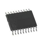
| 描述 | IC ADC 12BIT 2CH DUAL 20-TSSOP模数转换器 - ADC Dual 1MSPS 12-Bit 2-Ch SAR |
| DevelopmentKit | EVAL-CN0341-SDPZ |
| 产品分类 | |
| 品牌 | Analog Devices Inc |
| 产品手册 | |
| 产品图片 |
|
| rohs | 符合RoHS无铅 / 符合限制有害物质指令(RoHS)规范要求 |
| 产品系列 | 数据转换器IC,模数转换器 - ADC,Analog Devices AD7866ARUZ- |
| 数据手册 | |
| 产品型号 | AD7866ARUZ |
| 产品目录页面 | |
| 产品种类 | 模数转换器 - ADC |
| 位数 | 12 |
| 供应商器件封装 | 20-TSSOP |
| 信噪比 | 68 dB |
| 分辨率 | 12 bit |
| 包装 | 管件 |
| 商标 | Analog Devices |
| 安装类型 | 表面贴装 |
| 安装风格 | SMD/SMT |
| 封装 | Tube |
| 封装/外壳 | 20-TSSOP(0.173",4.40mm 宽) |
| 封装/箱体 | TSSOP-20 |
| 工作温度 | -40°C ~ 125°C |
| 工作电源电压 | 5 V |
| 工厂包装数量 | 75 |
| 接口类型 | Serial (SPI, QSPI, Microwire) |
| 数据接口 | DSP,MICROWIRE™,QSPI™,串行,SPI™ |
| 最大功率耗散 | 24 mW |
| 最大工作温度 | + 85 C |
| 最小工作温度 | - 40 C |
| 标准包装 | 75 |
| 特性 | 同步采样 |
| 电压参考 | Internal, External |
| 电压源 | 模拟和数字 |
| 系列 | AD7866 |
| 结构 | SAR |
| 转换器数 | 2 |
| 转换器数量 | 2 |
| 转换速率 | 1 MS/s |
| 输入数和类型 | 4 个单端,单极 |
| 输入类型 | Single-Ended |
| 通道数量 | 4 Channel |
| 配用 | /product-detail/zh/EVAL-AD7866CBZ/EVAL-AD7866CBZ-ND/1662764 |
| 采样率(每秒) | 1M |


.jpg)


- 商务部:美国ITC正式对集成电路等产品启动337调查
- 曝三星4nm工艺存在良率问题 高通将骁龙8 Gen1或转产台积电
- 太阳诱电将投资9.5亿元在常州建新厂生产MLCC 预计2023年完工
- 英特尔发布欧洲新工厂建设计划 深化IDM 2.0 战略
- 台积电先进制程称霸业界 有大客户加持明年业绩稳了
- 达到5530亿美元!SIA预计今年全球半导体销售额将创下新高
- 英特尔拟将自动驾驶子公司Mobileye上市 估值或超500亿美元
- 三星加码芯片和SET,合并消费电子和移动部门,撤换高东真等 CEO
- 三星电子宣布重大人事变动 还合并消费电子和移动部门
- 海关总署:前11个月进口集成电路产品价值2.52万亿元 增长14.8%


PDF Datasheet 数据手册内容提取
Dual 1 MSPS, 12-Bit, 2-Channel SAR ADC with Serial Interface AD7866 FEATURES FUNCTIONAL BLOCK DIAGRAM Dual 12-Bit, 2-Channel ADC Fast Throughput Rate: 1 MSPS VREF DCAPA REF SELECT AVDD DVDD Specified for V of 2.7V to 5.25V DD Low Power 2.5V BUF AD7866 11.4 mW Max at 1 MSPS with 3 V Supplies REF 24 mW Max at 1 MSPS with 5 V Supplies 12-BIT Wide Input Bandwidth VVAA21 MUX T/H APSPURCOCXEISMSAITVIEON DORUITVPEURTS DOUTA 70 dB SNR at 300 kHz Input Frequency ADC On-Board Reference 2.5 V A0 –40(cid:1)C to +125(cid:1)C Operation RANGE Flexible Power/Throughput Rate Management COLONTGRICOL SCLK CS Simultaneous Conversion/Read VDRIVE No Pipeline Delays HiMghIC SRpOeWedI RSEeTrMia/lD ISnPte Crfoamcep SatPiIbTlMe/QSPITM/ VVBB21 MUX T/H APSPURC1OC2X-EBISMITSAITVIEON DORUITVPEURTS DOUTB Shutdown Mode: 1 (cid:2)A Max ADC 20-Lead TSSOP Package BUF GENERAL DESCRIPTION AGND AGND DCAPB DGND The AD7866 is a dual 12-bit high speed, low power, successive approximation ADC. The part operates from a single 2.7 V to 5.25 V power supply and features throughput rates up to 1 MSPS. The device contains two ADCs, each preceded by a low noise, PRODUCT HIGHLIGHTS wide bandwidth track-and-hold amplifier that can handle 1. The AD7866 features two complete ADC functions, allowing input frequencies in excess of 10 MHz. simultaneous sampling and conversion of two channels. Each ADC has a 2-channel input multiplexer. The conversion result The conversion process and data acquisition are controlled of both channels is available simultaneously on separate data using standard control inputs, allowing easy interfacing to lines, or may be taken on one data line if only one serial port microprocessors or DSPs. The input signal is sampled on the is available. falling edge of CS; conversion is also initiated at this point. The conversion time is determined by the SCLK frequency. 2. High Throughput with Low Power Consumption—The There are no pipelined delays associated with the part. AD7866 offers a 1 MSPS throughput rate with 11.4 mW maximum power consumption when operating at 3 V. The AD7866 uses advanced design techniques to achieve very low power dissipation at high throughput rates. With 3 V 3. Flexible Power/Throughput Rate Management—The conver- supplies and 1 MSPS throughput rate, the part consumes a sion rate is determined by the serial clock, allowing the power maximum of 3.8 mA. With 5 V supplies and 1 MSPS, the consumption to be reduced as the conversion time is reduced current consumption is a maximum of 4.8 mA. The part also through a SCLK frequency increase. Power efficiency can be offers flexible power/throughput rate management when maximized at lower throughput rates if the part enters sleep operating in sleep mode. during conversions. The analog input range for the part can be selected to be a 0 V 4. No Pipeline Delay—The part features two standard successive to V range or a 2 (cid:1) V range with either straight binary or approximation ADCs with accurate control of the sampling REF REF twos complement output coding. The AD7866 has an on-chip instant via a CS input and once off conversion control. 2.5 V reference that can be overdriven if an external reference is preferred. Each on-board ADC can also be supplied with a separate individual external reference. The AD7866 is available in a 20-lead thin shrink small outline (TSSOP) package. REV.A Information furnished by Analog Devices is believed to be accurate and reliable. However, no responsibility is assumed by Analog Devices for its use, nor for any infringements of patents or other rights of third parties that may result from its use. No license is granted by implication or otherwise One Technology Way, P.O. Box 9106, Norwood, MA 02062-9106, U.S.A. under any patent or patent rights of Analog Devices. Trademarks and Tel: 781/329-4700 www.analog.com registered trademarks are the property of their respective companies. Fax: 781/326-8703 © 2003 Analog Devices, Inc. All rights reserved.
AD7866–SPECIFICATIONS (T = T to T , V = 2.7 V to 5.25 V, V = 2.7 V to 5.25 V, Reference = 2.5 V A MIN MAX DD DRIVE External on D A and D B, f = 20 MHz, unless otherwise noted.) CAP CAP SCLK Parameter A Version1 B Version1 Unit Test Conditions/Comments DYNAMIC PERFORMANCE Signal to Noise + Distortion (SINAD)2 68 68 dB min f = 300 kHz Sine Wave, f = 1 MSPS IN S Total Harmonic Distortion (THD)2 –75 –75 dB max f = 300 kHz Sine Wave, f = 1 MSPS IN S Peak Harmonic or Spurious Noise (SFDR)2 –76 –76 dB max f = 300 kHz Sine Wave, f = 1 MSPS IN S Intermodulation Distortion (IMD)2 Second Order Terms –88 –88 dB typ Third Order Terms –88 –88 dB typ Channel-to-Channel Isolation –88 –88 dB typ SAMPLE AND HOLD Aperture Delay3 10 10 ns max Aperture Jitter3 50 50 ps typ Aperture Delay Matching3 200 200 ps max Full Power Bandwidth 12 12 MHz typ @ 3 dB 2 2 MHz typ @ 0.1 dB DC ACCURACY Resolution 12 12 Bits Integral Nonlinearity ±1.5 ±1 LSB max B Grade, 0 V to V Range Only; ±0.5 LSB typ REF ±1.5 LSB max 0 V to 2 (cid:1) V Range; ±0.5 LSB typ REF Differential Nonlinearity –0.95/+1.25 –0.95/+1.25 LSB max Guaranteed No Missed Codes to 12 Bits 0 V to V Input Range Straight Binary Output Coding REF Offset Error ±8 ±8 LSB max Offset Error Match ±1.2 ±1.2 LSB typ Gain Error ±2.5 ±2.5 LSB max Gain Error Match ±0.2 ±0.2 LSB typ 2 (cid:1) V Input Range –V to +V Biased about V with REF REF REF REF Positive Gain Error ±2.5 ±2.5 LSB max Twos Complement Output Coding Zero Code Error ±8 ±8 LSB max Zero Code Error Match ±0.2 ±0.2 LSB typ Negative Gain Error ±2.5 ±2.5 LSB max ANALOG INPUT Input Voltage Ranges 0 to V 0 to V V RANGE Pin Low upon CS Falling Edge REF REF 0 to 2 (cid:1) V 0 to 2 (cid:1) V V RANGE Pin High upon CS Falling Edge REF REF DC Leakage Current ±500 ±500 nA max T = –40(cid:2)C to +85(cid:2)C A 1 1 µA max 85(cid:2)C < T ≤ 125(cid:2)C A Input Capacitance 30 30 pF typ When in Track 10 10 pF typ When in Hold REFERENCE INPUT/OUTPUT Reference Input Voltage 2.5 2.5 V ±1% for Specified Performance Reference Input Voltage Range4 2/3 2/3 V min/V max REF SELECT Pin Tied High DC Leakage Current ±30 ±30 µA max V Pin REF ±160 ±160 µA max D A, D B Pins CAP CAP Input Capacitance 20 20 pF typ Reference Output Voltage5 2.45/2.55 2.45/2.55 V min/V max V Output Impedance6 25 25 Ω typ V = 5 V REF DD 45 45 Ω typ V = 3 V DD Reference Temperature Coefficient 50 50 ppm/°C typ REF OUT Error (T to T ) ±15 ±15 mV typ MIN MAX LOGIC INPUTS Input High Voltage, V 0.7 V 0.7 V V min INH DRIVE DRIVE Input Low Voltage, V 0.3 V 0.3 V V max INL DRIVE DRIVE Input Current, I ±1 ±1 µA max Typically 15 nA, V = 0 V or V IN IN DRIVE Input Capacitance, C 3 10 10 pF max IN LOGIC OUTPUTS Output High Voltage, V V – 0.2 V – 0.2 V min I = 200 µA OH DRIVE DRIVE SOURCE Output Low Voltage, V 0.4 0.4 V max I = 200 µA OL SINK Floating-State Leakage Current ±1 ±1 µA max V = 2.7 V to 5.25 V DD Floating-State Output Capacitance3 10 10 pF max Output Coding Straight (Natural) Binary Selectable with Either Input Range Twos Complement –2– REV. A
AD7866 Parameter A Version1 B Version1 Unit Test Conditions/Comments CONVERSION RATE Conversion Time 16 16 SCLK cycles 800 ns with SCLK = 20 MHz Track/Hold Acquisition Time3 300 300 ns max Throughput Rate 1 1 MSPS max See Serial Interface Section POWER REQUIREMENTS V 2.7/5.25 2.7/5.25 V min/max DD V 2.7/5.25 2.7/5.25 V min/max DRIVE I 7 Digital I/Ps = 0 V or V DD DRIVE Normal Mode (Static) 3.1 3.1 mA max V = 4.75 V to 5.25 V. Add 0.5 mA DD Typical if Using Internal Reference. 2.8 2.8 mA max V = 2.7 V to 3.6 V. Add 0.35 mA DD Typical if Using Internal Reference. Operational, f = 1 MSPS 4.8 4.8 mA max V = 4.75 V to 5.25 V. Add 0.5 mA S DD Typical if Using Internal Reference. 3.8 3.8 mA max V = 2.7 V to 3.6 V. Add 0.5 mA DD Typical if Using Internal Reference. Partial Power-Down Mode 1.6 1.6 mA max f = 100 kSPS, f = 20 MHz S SCLK Add 0.2 mA Typ if Using Internal Reference. Partial Power-Down Mode 560 560 µA max (Static) Add 100 µA Typical if Using Internal Reference. Full Power-Down Mode 1 1 µA max SCLK On or Off. T = –40(cid:2)C to +85(cid:2)C A 2 2 µA max SCLK On or Off. 85(cid:2)C < T ≤ 125(cid:2)C A Power Dissipation7 Normal Mode (Operational) 24 24 mW max V = 5 V DD 11.4 11.4 mW max V = 3 V DD Partial Power-Down (Static) 2.8 2.8 mW max V = 5 V. SCLK On or Off. DD 1.68 1.68 mW max V = 3 V. SCLK On or Off. DD Full Power-Down (Static) 5 5 µW max V = 5 V. SCLK On or Off. DD 3 3 µW max V = 3 V. SCLK On or Off. DD NOTES 1Temperature ranges as follows: A, B Versions: –40°C to +125°C. 2See Terminology section. 3Sample tested @ 25°C to ensure compliance. 4External reference range that may be applied at V , D A, or D B. REF CAP CAP 5Relates to pins V , D A, or D B. REF CAP CAP 6See Reference section for D A, D B output impedances. CAP CAP 7See Power vs. Throughput Rate section. Specifications subject to change without notice. REV. A –3–
AD7866 TIMING SPECIFICATIONS1 (V = 2.7 V to 5.25 V, V = 2.7 V to 5.25 V, V = 2.5 V; T = T to T , unless otherwise noted.) DD DRIVE REF A MIN MAX Limit at Parameter T , T Unit Description MIN MAX f 2 10 kHz min SCLK 20 MHz max t 16 (cid:1) t ns max t = 1/f CONVERT SCLK SCLK SCLK 800 ns max f = 20 MHz SCLK t 50 ns max Minimum Time between End of Serial Read and Next Falling Edge of CS QUIET t 10 ns min CS to SCLK Setup Time 2 t 3 25 ns max Delay from CS until D A and D B Three-State Disabled 3 OUT OUT t 3 40 ns max Data Access Time after SCLK Falling Edge. V (cid:3)3 V, C = 50 pF; 4 DRIVE L V < 3V, C = 25 pF DRIVE L t 0.4 t ns min SCLK Low Pulsewidth 5 SCLK t 0.4 t ns min SCLK High Pulsewidth 6 SCLK t 10 ns min SCLK to Data Valid Hold Time 7 t 4 25 ns max CS Rising Edge to D A, D B, High Impedance 8 OUT OUT t 4 10 ns min SCLK Falling Edge to D A, D B, High Impedance 9 OUT OUT 50 ns max SCLK Falling Edge to D A, D B, High Impedance OUT OUT NOTES 1Sample tested at 25°C to ensure compliance. All input signals are specified with t = t = 5 ns (10% to 90% of V ) and timed from a voltage level of 1.6 V. R F DRIVE 2Mark/Space ratio for the CLK input is 40/60 to 60/40. 3Measured with the load circuit of Figure 1 and defined as the time required for the output to cross 0.8 V or 2.0 V. 4t t are derived from the measured time taken by the data outputs to change 0.5 V when loaded with the circuit of Figure 1. The measured number is then extrapo- 8, 9 lated back to remove the effects of charging or discharging the 50 pF capacitor. This means that the times t and t quoted in the timing characteristics are the true 8 9 bus relinquish times of the part and are independent of the bus loading. Specifications subject to change without notice. 200(cid:2)A IOL TO OUTPUT 1.6V PIN CL 50pF 200(cid:2)A IOH Figure 1.Load Circuit for Digital Output Timing Specifications –4– REV. A
AD7866 ABSOLUTE MAXIMUM RATINGS1 Storage Temperature Range . . . . . . . . . . . . –65(cid:2)C to +150(cid:2)C (T = 25oC, unless otherwise noted.) Junction Temperature . . . . . . . . . . . . . . . . . . . . . . . . . . 150(cid:2)C A AV to AGND . . . . . . . . . . . . . . . . . . . . . . . . .–0.3 V to +7 V TSSOP Package, Power Dissipation . . . . . . . . . . . . . 450 mW DD DV to DGND . . . . . . . . . . . . . . . . . . . . . . . .–0.3 V to +7 V (cid:5) Thermal Impedance (TSSOP) . . . . . . . . . . . . . 143(cid:2)C/W DD JA V to DGND . . . . . . . . . . . . . . . . –0.3 V to DV + 0.3 V (cid:5) Thermal Impedance (TSSOP) . . . . . . . . . . . . . . 45(cid:2)C/W DRIVE DD JC V to AGND . . . . . . . . . . . . . . . . –0.3 V to AV + 0.3 V Lead Temperature, Soldering DRIVE DD AV to DV . . . . . . . . . . . . . . . . . . . . . . . . –0.3 V to +0.3 V Vapor Phase (60 sec) . . . . . . . . . . . . . . . . . . . . . . . . . 215(cid:2)C DD DD AGND to DGND . . . . . . . . . . . . . . . . . . . . . –0.3 V to +0.3 V Infrared (15 sec) . . . . . . . . . . . . . . . . . . . . . . . . . . . . 220(cid:2)C Analog Input Voltage to AGND . . . . .–0.3 V to AV + 0.3 V ESD . . . . . . . . . . . . . . . . . . . . . . . . . . . . . . . . . . . . . . 1.5 kV DD Digital Input Voltage to DGND . . . . . . . . . . . .–0.3 V to +7 V V to AGND . . . . . . . . . . . . . . . . . .–0.3 V to AV + 0.3 V NOTES REF DD Digital Output Voltage to DGND . . . –0.3 V to V + 0.3 V 1Stresses above those listed under Absolute Maximum Ratings may cause perma- DRIVE Input Current to Any Pin Except Supplies2 . . . . . . . . .(cid:4)10 mA nent damage to the device. This is a stress rating only; functional operation of the device at these or any other conditions above those listed in the operational Operating Temperature Range sections of this specification is not implied. Exposure to absolute maximum rating Commercial (A, B Versions) . . . . . . . . . . . . .–40(cid:2)C to +125(cid:2)C conditions for extended periods may affect device reliability. 2Transient currents of up to 100 mA will not cause SCR latch up. ORDERING GUIDE Resolution Package Model Temperature Range (Bits) Package Description Option AD7866ARU –40°C to +125°C 12 Thin Shrink SOC (TSSOP) RU-20 AD7866BRU –40°C to +125°C 12 Thin Shrink SOC (TSSOP) RU-20 EVAL-AD7866CB1 Evaluation Board EVAL-CONTROL BRD22 Controller Board NOTES 1This can be used as a standalone evaluation board or in conjunction with the evaluation board controller for evaluation/demonstration purposes. 2This evaluation board controller is a complete unit, allowing a PC to control and communicate with all Analog Devices evaluation boards ending in the CB designators. To order a complete evaluation kit, the particular ADC evaluation board, e.g., EVAL-AD7866CB, the EVAL-CONTROL BRD2, and a 12 V transformer must be ordered. See relevant Evaluation Board Technical note for more information. CAUTION ESD (electrostatic discharge) sensitive device. Electrostatic charges as high as 4000 V readily accumulate on the human body and test equipment and can discharge without detection. Although the AD7866 features proprietary ESD protection circuitry, permanent damage may occur on devices subjected to high energy electrostatic discharges. Therefore, proper ESD precautions are recommended to avoid performance degradation or loss of functionality. REV. A –5–
AD7866 PIN CONFIGURATION REF SELECT 1 20 A0 DCAPB 2 19 CS AGND 3 18 SCLK VB2 4 17 VDRIVE VB1 5 AD7866 16 DOUTB VA2 6 (NToOt Pto V SIEcaWle)15 DOUTA VA1 7 14 DGND AGND 8 13 DVDD DCAPA 9 12 AVDD VREF 10 11 RANGE PIN FUNCTION DESCRIPTIONS Pin No. Mnemonic Function 1 REF SELECT Internal/External Reference Selection. Logic input. If this pin is tied to GND, the on-chip 2.5 V reference is used as the reference source for both ADC A and ADC B. In addition, pins V , D A, and D B REF CAP CAP must be tied to decoupling capacitors. If the REF SELECT pin is tied to a logic high, an external refer- ence can be supplied to the AD7866 through the V pin, in which case decoupling capacitors are REF required on D A and D B. However, if the V pin is tied to AGND while REF SELECT is tied to CAP CAP REF a logic low, an individual external reference can be applied to both ADC A and ADC B through pins D A and D B, respectively. See the Reference Configuration Options section. CAP CAP 2, 9 D B, D A Decoupling capacitors are connected to these pins to decouple the reference buffer for each respective CAP CAP ADC. The on-chip reference can be taken from these pins and applied externally to the rest of a system. Depending on the polarity of the REF SELECT pin and the configuration of the V pin, these REF pins can also be used to input a separate external reference to each ADC. The range of the external reference is dependent on the analog input range selected. See the Reference Configuration Options section. 3, 8 AGND Analog Ground. Ground reference point for all analog circuitry on the AD7866. All analog input signals and any external reference signal should be referred to this AGND voltage. Both of these pins should connect to the AGND plane of a system. The AGND and DGND voltages ideally should be at the same potential and must not be more than 0.3 V apart, even on a transient basis. 4, 5 V ,V Analog Inputs of ADC B. Single-ended analog input channels. The input range on each channel is 0 V B2 B1 to V or a 2 (cid:1) V range depending on the polarity of the RANGE pin upon the falling edge of CS. REF REF 6, 7 V ,V Analog Inputs of ADC A. Single-ended analog input channels. The input range on each channel is 0 V A2 A1 to V or a 2 (cid:1) V range depending on the polarity of the RANGE pin upon the falling edge of CS. REF REF 10 V Reference Decoupling and External Reference Selection. This pin is connected to the internal reference REF and requires a decoupling capacitor. The nominal reference voltage is 2.5 V, which appears at the pin; however, if the internal reference is to be used externally in a system, it must be taken from either the D A or D B pins. This pin is also used in conjunction with the REF SELECT pin when CAP CAP applying an external reference to the AD7866. See the REF SELECT pin description. –6– REV. A
AD7866 PIN FUNCTION DESCRIPTIONS (continued) Pin No. Mnemonic Function 11 RANGE Analog Input Range and Output Coding Selection. Logic input. The polarity on this pin will determine what input range the analog input channels on the AD7866 will have, and will also select the type of output coding the ADC will use for the conversion result. On the falling edge of CS, the polarity of this pin is checked to determine the analog input range of the next conversion. If this pin is tied to a logic low, the analog input range is 0 V to V and the output coding from the part will REF be straight binary (for the next conversion). If this pin is tied to a logic high when CS goes low, the analog input range is 2 (cid:1) V and the output coding for the part will be twos complement. How- REF ever, if after the falling edge of CS the logic level of the RANGE pin has changed upon the eighth SCLK falling edge, the output coding will change to the other option without any change in the analog input range. (See the Analog Input and ADC Transfer Function sections.) 12 AV Analog Supply Voltage, 2.7 V to 5.25 V. This is the only supply voltage for all analog circuitry on the DD AD7866. The AV and DV voltages ideally should be at the same potential and must not be DD DD more than 0.3 V apart even on a transient basis. This supply should be decoupled to AGND. 13 DV Digital Supply Voltage, 2.7 V to 5.25 V. This is the supply voltage for all digital circuitry on the DD AD7866. The DV and AV voltages should ideally be at the same potential and must not be DD DD more than 0.3 V apart even on a transient basis. This supply should be decoupled to DGND. 14 DGND Digital Ground. This is the ground reference point for all digital circuitry on the AD7866. The DGND and AGND voltages ideally should be at the same potential and must not be more than 0.3 V apart even on a transient basis. 15, 16 D A, D B Serial Data Outputs. The data output is supplied to this pin as a serial data stream. The bits are OUT OUT clocked out on the falling edge of the SCLK input. The data appears on both pins simultaneously from the simultaneous conversions of both ADCs. The data stream consists of one leading zero followed by three STATUS bits, followed by the 12 bits of conversion data. The data is provided MSB first. If CS is held low for another 16 SCLK cycles after the conversion data has been output on either D A or D B, the data from the other ADC follows on the D pin. This allows data OUT OUT OUT from a simultaneous conversion on both ADCs to be gathered in serial format on either D A or OUT D B alone using only one serial port. See the Serial Interface section. OUT 17 V Logic Power Supply Input. The voltage supplied at this pin determines at what voltage the interface DRIVE will operate. This pin should be decoupled to DGND. 18 SCLK Serial Clock. Logic Input. A serial clock input provides the SCLK for accessing the data from the AD7866. This clock is also used as the clock source for the conversion process. 19 CS Chip Select. Active low logic input. This input provides the dual function of initiating conversions on the AD7866 and frames the serial data transfer. 20 A0 Multiplexer Select. Logic input. This input is used to select the pair of channels to be converted simultaneously, i.e., Channel 1 of both ADC A and ADC B, or Channel 2 of both ADC A and ADC B. The logic state of this pin is checked upon the falling edge of CS, and the multiplexer is set up for the next conversion. If it is low, the following conversion will be performed on Channel 1 of each ADC; if it is high, the following conversion will be performed on Channel 2 of each ADC. REV. A –7–
AD7866 TERMINOLOGY the fundamental. Noise is the sum of all nonfundamental sig- nals up to half the sampling frequency (f /2), excluding dc. The Integral Nonlinearity S ratio is dependent on the number of quantization levels in the This is the maximum deviation from a straight line passing digitization process; the more levels, the smaller the quantiza- through the endpoints of the ADC transfer function. The tion noise. The theoretical signal-to-(noise + distortion) ratio endpoints of the transfer function are zero scale, a point 1 LSB for an ideal N-bit converter with a sine wave input is given by: below the first code transition, and full scale, a point 1 LSB above the last code transition. Signal-to-(Noise + Distortion) = (6.02N + 1.76)dB Differential Nonlinearity Thus, for a 12-bit converter, this is 74dB. This is the difference between the measured and the ideal 1 LSB Total Harmonic Distortion (THD) change between any two adjacent codes in the ADC. Total harmonic distortion is the ratio of the rms sum of har- Offset Error monics to the fundamental. For the AD7866, it is defined as: This applies to Straight Binary output coding. It is the deviation of the first code transition (00 . . . 000) to (00 . . . 001) from the THD(db)=20log V22+V32+V42+V52+V62 ideal, i.e., AGND + 1 LSB. V 1 Offset Error Match where V is the rms amplitude of the fundamental and V , V , 1 2 3 This is the difference in Offset Error between the two channels. V , V , and V are the rms amplitudes of the second through the 4 5 6 sixth harmonics. Gain Error This applies to Straight Binary output coding. It is the deviation Peak Harmonic or Spurious Noise of the last code transition (111 . . . 110) to (111 . . . 111) from Peak harmonic, or spurious noise, is defined as the ratio of the the ideal (i.e., V – 1 LSB) after the offset error has been rms value of the next largest component in the ADC output REF adjusted out. spectrum (up to f /2 and excluding dc) to the rms value of the S fundamental. Normally, the value of this specification is deter- Gain Error Match This is the difference in Gain Error between the two channels. mined by the largest harmonic in the spectrum. But for ADCs where the harmonics are buried in the noise floor, it will be a Zero Code Error noise peak. This applies when using the twos complement output coding option, in particular with the 2 (cid:1) V input range as –V to Intermodulation Distortion REF REF +V biased about the V point. It is the deviation of the With inputs consisting of sine waves at two frequencies, fa and fb, REF REF midscale transition (all 1s to all 0s) from the ideal V voltage, any active device with nonlinearities will create distortion products i.e., V – 1 LSB. IN at sum and difference frequencies of mfa ± nfb where m, n = 0, REF 1, 2, 3, and so on. Intermodulation distortion terms are those for Zero Code Error Match which neither m nor n are equal to zero. For example, the second This refers to the difference in Zero Code Error between the order terms include (fa + fb) and (fa – fb), while the third order two channels. terms include (2fa + fb), (2fa – fb), (fa + 2fb), and (fa – 2fb). Positive Gain Error The AD7866 is tested using the CCIF standard where two This applies when using the twos complement output coding input frequencies near the top end of the input bandwidth are option, in particular with the 2 (cid:1) V input range as –V to REF REF used. In this case, the second order terms are usually distanced +V biased about the V point. It is the deviation of the last REF REF in frequency from the original sine waves while the third order code transition (011 . . . 110) to (011 . . . 111) from the ideal terms are usually at a frequency close to the input frequencies. (i.e., +V – 1 LSB) after the Zero Code Error has been REF As a result, the second and third order terms are specified sepa- adjusted out. rately. The calculation of the intermodulation distortion is as Negative Gain Error per the THD specification where it is the ratio of the rms sum This applies when using the twos complement output coding of the individual distortion products to the rms amplitude of the option, in particular with the 2 (cid:1) V input range as –V to sum of the fundamentals expressed in dB. REF REF +V biased about the V point. It is the deviation of the first REF REF Channel-to-Channel Isolation code transition (100 . . . 000) to (100 . . . 001) from the ideal Channel-to-channel isolation is a measure of the level of crosstalk (i.e., –V + 1 LSB) after the Zero Code Error has been REF between channels. It is measured by applying a full-scale adjusted out. (2 (cid:1) V ), 455kHz sine wave signal to all unselected input REF Track-and-Hold Acquisition Time channels and determining how much that signal is attenuated in the The track-and-hold amplifier returns into track mode after the selected channel with a 10 kHz signal (0 V to V ). The figure REF end of conversion. Track-and-hold acquisition time is the time given is the worst-case across all four channels for the AD7866. required for the output of the track-and-hold amplifier to reach PSR (Power Supply Rejection) its final value, within ±1/2 LSB, after the end of conversion. See the Performance Curves section. Signal-to-(Noise + Distortion) Ratio (SNDR) This is the measured ratio of signal-to-(noise + distortion) at the output of the A/D converter. The signal is the rms amplitude of –8– REV. A
AD7866 PERFORMANCE CURVES Pf = power at frequency f in ADC output, and PfS = power at TPC 1 shows a typical FFT plot for the AD7866 at 1 MHz frequency fS coupled onto the ADC AVDD supply. Here, a 100 mV sample rate and 300 kHz input frequency. TPC 2 shows the peak-to-peak sine wave is coupled onto the AVDD supply while the signal-to-(noise + distortion) ratio performance versus input digital supply is left unaltered. TPCs 3a and 3b show the PSRR frequency for various supply voltages while sampling at 1 MSPS of the AD7866 when there is no decoupling on the supply, while with an SCLK of 20 MHz. TPCs 4a and 4b show the PSRR with decoupling capacitors of 10 µF and 0.1 µF on the supply. TPCs 3a to 4b show the power supply rejection ratio versus AV supply ripple frequency for the AD7866 under different TPCs 5 and 6 show typical DNL and INL plots for the AD7866. DD conditions. The power supply rejection ratio (PSRR) is defined TPC 7 shows a graph of the total harmonic distortion versus as the ratio of the power in the ADC output at full-scale fre- analog input frequency for various source impedances. quency f, to the power of a 100 mV sine wave applied to the TPC 8 shows a graph of total harmonic distortion versus analog ADC AV supply of frequency f : DD S input frequency for various supply voltages. See the Analog ( ) ( ) PSRR dB =10log Pf Pf Input section. S Typical Performance Characteristics 0 0 –15 4SffSI0NNA9 R=M8 P3=PL0 O7E00 Ik=N.H3 T11zM dFBSFPTS ––2100 12T0.A50 V=m E2V5X (cid:1)pTC- pR ESFINEER WENACVEE OONN VARVEDFD THD = –85.47dB –35 SFDR = –86.64dB –30 B –40 B d NR – d–55 SRR – –50 VDD = 5.25V VDD = 2.7V S P –60 –75 –70 –95 –80 VDD = 4.75V –90 VDD = 3.6V –115 –100 0 50 100 150 200 250 300 350 400 450 500 1k 10k 100k 1M FREQUENCY – kHz AVDD RIPPLE FREQUENCY – Hz TPC 1.Dynamic Performance TPC 3a.PSRR vs. Supply Ripple Frequency, without Supply Decoupling –61 TA = 25C 0 100mV p-p SINE WAVE ON AVDD –63 –10 2.5V EXT REFERENCE ON DCAPA, DCAPB TA = 25(cid:1)C –20 –65 VDD = VDRIVE = 2.7V –30 B SINAD – d ––6679 VDD = VDRIVE = 3.6V PSRR – dB –––465000 VDD = 2.7V VDD = 5.25V –71 VDD = VDRIVE = 5.25V –70 VDD = VDRIVE = 4.75V –80 –73 –90 –7510k 100k 1M –100 VDD = 4.75V VDD = 3.6V 1k 10k 100k 1M INPUT FREQUENCY – Hz AVDD RIPPLE FREQUENCY – Hz TPC 2.SINAD vs. Input Frequency TPC 3b.PSRR vs. Supply Ripple Frequency, without Supply Decoupling REV. A –9–
AD7866 0 1.0 100mV p-p SINE WAVE ON AVDD –10 2.5V EXT REFERENCE ON VREF 0.8 –20 TA = 25(cid:1)C 0.6 –30 0.4 B –40 B 0.2 – d LS R –50 – 0.0 R L S N P –60 I–0.2 VDD = 2.7V –70 –0.4 –80 –0.6 VDD = 3.6V –90 –0.8 –100 –1.0 1k 10k 100k 1M 0 500 1000 1500 2000 2500 3000 3500 4000 AVDD RIPPLE FREQUENCY – Hz ADC – Code TPC 4a.PSRR vs. Supply Ripple Frequency, TPC 6.DC INL Plot with Supply Decoupling –100 120.50Vm EVX pT- pR ESFINEER WENACVEE OONN DACVADPDA, DCAPB –60 TVAD D= =2 54(cid:1).C75V RIN = 100(cid:3) –20 TA = 25(cid:1)C –65 RIN = 50(cid:3) –30 –70 B –40 B – d – d–75 RIN = 10(cid:3) R –50 D R H PS –60 VDD = 2.7V T –80 –70 –80 –85 VDD = 3.6V –90 VDD = 4.75V –90 –100 10k 100k 1000k 1k 10k 100k 1M INPUT FREQUENCY – Hz AVDD RIPPLE FREQUENCY – Hz TPC 7.THD vs. Analog Input Frequency TPC 4b.PSRR vs. Supply Ripple Frequency, for Various Source Impedances with Supply Decoupling –70 1.0 –72 TA = 25(cid:1)C VDD = VDRIVE = 2.7V 0.8 0.6 –74 VDD = VDRIVE = 3.6V –76 0.4 –78 – LSB 0.20 D – dB–80 NL TH–82 D–0.2 –84 –0.4 VDD = VDRIVE = 5.25V –86 –0.6 –0.8 –88 VDD = VDRIVE = 4.75V –1.0 –9010k 100k 1000k 0 500 1000 1500 2000 2500 3000 3500 4000 INPUT FREQUENCY – Hz ADC – Code TPC 5.DC DNL Plot TPC 8.THD vs. Analog Input Frequency for Various Supply Voltages –10– REV. A
AD7866 CIRCUIT INFORMATION CAPACITIVE The AD7866 is a fast, micropower, dual 12-bit, single supply, DAC A/D converter that operates from a 2.7 V to 5.25 V supply. When operated from either a 5 V supply or a 3 V supply, the A VIN CONTROL AD7866 is capable of throughput rates of 1 MSPS when provided SW1 B LOGIC with a 20 MHz clock. SW2 COMPARATOR The AD7866 contains two on-chip track-and-hold amplifiers, two successive approximation A/D converters, and a serial inter- AGND face with two separate data output pins, and is housed in a Figure 3.ADC Conversion Phase 20-lead TSSOP package, which offers the user considerable space-saving advantages over alternative solutions. The serial ANALOG INPUT clock input accesses data from the part but also provides the Figure 4 shows an equivalent circuit of the analog input structure clock source for each successive approximation ADC. The ana- of the AD7866. The two diodes, D1 and D2, provide ESD log input range for the part can be selected to be a 0 V to V protection for the analog inputs. Care must be taken to ensure REF input or a 2 (cid:1) V input with either straight binary or twos that the analog input signal never exceeds the supply rails by more REF complement output coding. The AD7866 has an on-chip 2.5 V than 300 mV. This will cause these diodes to become forward- reference that can be overdriven if an external reference is pre- biased and start conducting current into the substrate. 10 mA is ferred. In addition, each ADC can be supplied with an individual the maximum current these diodes can conduct without causing separate external reference. irreversible damage to the part. The capacitor C1 in Figure 4 is typically about 10 pF and can primarily be attributed to pin The AD7866 also features power-down options to allow power capacitance. The resistor R1 is a lumped component made up saving between conversions. The power-down feature is imple- of the on resistance of a switch. This resistor is typically about mented across the standard serial interface, as described in the 100 Ω. The capacitor C2 is the ADC sampling capacitor and Modes of Operation section. has a capacitance of 20 pF typically. For ac applications, removing high frequency components from the analog input signal is CONVERTER OPERATION recommended by use of an RC low-pass filter on the relevant The AD7866 has two successive approximation analog-to-digital analog input pin. In applications where harmonic distortion and converters, each based around a capacitive DAC. Figures 2 and signal-to-noise ratio are critical, the analog input should be driven 3 show simplified schematics of one of these ADCs. The ADC from a low impedance source. Large source impedances will is comprised of control logic, a SAR, and a capacitive DAC, all significantly affect the ac performance of the ADC. This may of which are used to add and subtract fixed amounts of charge necessitate the use of an input buffer amplifier. The choice of the from the sampling capacitor to bring the comparator back into a op amp will be a function of the particular application. balanced condition. Figure 2 shows the ADC during its acquisition phase. SW2 is closed and SW1 is in position A, the comparator is held in a balanced condition, and the sampling capacitor VDD acquires the signal on V , for example. A1 D1 R1 C2 CAPACITIVE VIN DAC C1 D2 A VIN SW1 CONTROL B LOGIC CONVERT PHASE – SWITCH OPEN TRACK PHASE – SWITCH CLOSED SW2 COMPARATOR Figure 4.Equivalent Analog Input Circuit AGND When no amplifier is used to drive the analog input, the source Figure 2.ADC Acquisition Phase impedance should be limited to low values. The maximum source impedance will depend on the amount of total harmonic When the ADC starts a conversion (see Figure 3), SW2 will distortion (THD) that can be tolerated. The THD will increase open and SW1 will move to position B, causing the comparator as the source impedance increases, and performance will degrade to become unbalanced. The Control Logic and the capacitive (see TPC 7). DAC are used to add and subtract fixed amounts of charge from the sampling capacitor to bring the comparator back into a balanced condition. When the comparator is rebalanced, the conversion is complete. The Control Logic generates the ADC output code. Figures 10 and 11 show the ADC transfer functions. REV. A –11–
AD7866 Analog Input Ranges that the analog input range selected must not exceed V . The DD The analog input range for the AD7866 can be selected to be 0 V logic input A0 is used to select the pair of channels to be converted to V or 2 (cid:1) V with either straight binary or twos complement simultaneously. The logic state of this pin is also checked upon REF REF output coding. The RANGE pin is used to select both the analog the falling edge of CS, and the multiplexers are set up for the input range and the output coding, as shown in Figures 5 to 8. next conversion. If it is low, the following conversion will be On the falling edge of CS, point A, the logic level of the RANGE performed on Channel 1 of each ADC; if it is high, the following pin is checked to determine the analog input range of the next conversion will be performed on Channel 2 of each ADC. conversion. If this pin is tied to a logic low, the analog input Handling Bipolar Input Signals range will be 0 V to VREF and the output coding from the part will Figure 9 shows how useful the combination of the 2 (cid:1) V be straight binary (for the next conversion). If this pin is at a logic REF input range and the twos complement output coding scheme is high when CS goes low, the analog input range will be 2 (cid:1) V and REF for handling bipolar input signals. If the bipolar input signal the output coding for the part will be twos complement. How- is biased about V and twos complement output coding is ever, if after the falling edge of CS, the logic level of the REF selected, then V becomes the zero code point, –V is RANGE pin has changed upon the eighth falling SCLK edge, REF REF negative full-scale, and +V becomes positive full-scale with a point B, the output coding will change to the other option without dynamic range of 2 (cid:1) V RE.F any change in the analog input range. So for the next conversion, REF twos complement output coding could be selected with a 0 V to Transfer Functions V input range, for example, if the RANGE pin is low upon The designed code transitions occur at successive integer LSB REF the falling edge of CS and high upon the eighth falling SCLK values (i.e., 1 LSB, 2 LSB, and so on). The LSB size is VREF/4096. The ideal transfer characteristic for the AD7866 when straight edge, as shown in Figure 7. Figures 5 to 8 show examples of timing diagrams for selections of different analog input ranges binary coding is selected is shown in Figure 10, and the ideal with various output coding formats. Table I summarizes the transfer characteristic for the AD7866 when twos complement required logic level of the RANGE pin for each selection. Note coding is selected is shown in Figure 11. Table I. Analog Input and Output Coding Selection Range Level Range Level @ Point A1 @ Point B2 Input Range3 Output Coding3 Low Low 0 V to V Straight Binary REF High High V ± V Twos Complement REF REF Low High V /2 ± V /2 Twos Complement REF REF High Low 0 V to 2 (cid:1) V Straight Binary REF NOTES 1Point A = Falling edge of CS. 2Point B = Eighth falling edge of SCLK. 3Selected for next conversion. A B CS 0V TO V REF INPUT RANGE 1 8 16 1 16 SCLK RANGE DOUTA STRAIGHT BINARY DOUTB Figure 5.Selecting 0 V to V Input Range with Straight Binary Output Coding REF A B CS V (cid:4) V REF REF INPUT RANGE 1 8 16 1 16 SCLK RANGE DOUTA TWOS COMPLEMENT DOUTB Figure 6. Selecting V ± V Input Range with Twos Complement Output Coding REF REF –12– REV. A
AD7866 A B CS V /2 (cid:4) V /2 REF REF INPUT RANGE 1 8 16 1 16 SCLK RANGE DOUTA TWOS COMPLEMENT DOUTB Figure 7.Selecting V /2 ± V /2 Input Range with Twos Complement Output Coding REF REF A B CS 0V TO 2 (cid:5) V REF INPUT RANGE 1 8 16 1 16 SCLK RANGE DOUTA STRAIGHT BINARY DOUTB Figure 8.Selecting 0 V to 2 (cid:1) V Input Range with Straight Binary Output Coding REF VREF VDD 100nF REF SELECT VDD VREF DCAPA V R4 470nF DCAPB VDRIVE DSP/(cid:2)P 470nF R3 AD7866 COMTPWLOEMSENT R2 VIN DOUT 0V V R1 +VREF (= 2 (cid:5) VREF) 011 111 R1 = R2 = R3 = R4 VREF 000 000 (= 0V) –VREF 100 000 Figure 9. Handling Bipolar Signals with the AD7866 1LSB = 2 (cid:5) VREF/4096 011...111 011...110 111...111 111...110 DE 000...001 CO 000...000 CODE 111...000 1LSB = VREF/4096 ADC 111...111 DC 011...111 100...010 A 100...001 100...000 000...010 000...001 000...000 –VREF + 1LSB +VREF – 1LSB 0V 1LSB VREF – 1LSB VREF – 1LSB ANALOG INPUT ANALOG INPUT Figure 10.Straight Binary Transfer Figure 11.Twos Complement Transfer Characteristic with 0V to V Input Range Characteristic with V ± V Input Range REF REF REF REV. A –13–
AD7866 Digital Inputs The digital inputs applied to the AD7866 are not limited by the DCAPA 470nF maximum ratings that limit the analog inputs. Instead, the digital AD7866 inputs applied can go to 7 V and are not restricted by the VDD + 470nF DCAPB 0.3 V limit as on the analog inputs. See maximum ratings. Another advantage of SCLK, RANGE, REF SELECT, A0, and 100nF VREF CS not being restricted by the V + 0.3 V limit is that power DD supply sequencing issues are avoided. If one of these digital inputs Figure 12.Relevant Connections when Using an is applied before VDD, there is no risk of latch-up, as there Internal Reference would be on the analog inputs if a signal greater than 0.3 V were applied prior to V . DD V DCAPA TDhReI VAED7866 also has the V feature, which controls the VREF AD7866 DRIVE voltage at which the serial interface operates. V allows the DCAPB DRIVE ADC to easily interface to both 3 V and 5 V processors. For example, if the AD7866 was operated with a V of 5 V, the VREF REF SELECT DD V pin could be powered from a 3 V supply, allowing a large DRIVE dynamic range with low voltage digital processors. For example, Figure 13.Relevant Connections when Applying the AD7866 could be used with the 2 (cid:1) VREF input range, with a an External Reference at DCAPA and/or DCAPB V of 5 V while still being able to interface to 3 V digital parts. DD REFERENCE CONFIGURATION OPTIONS DCAPA 470nF The AD7866 has various reference configuration options. The AD7866 REF SELECT pin allows the choice of using an internal 2.5 V DCAPB VDRIVE 470nF reference or applying an external reference, or even an individual REF SELECT external reference for each on-chip ADC if desired. If the REF VREF VREF SELECT pin is tied to AGND, then the on-chip 2.5 V reference is used as the reference source for both ADC A and ADC B. In Figure 14.Relevant Connections when Applying addition, pins V , D A, and D B must be tied to decoupling REF CAP CAP an External Reference at V capacitors (100 nF, 470 nF, and 470 nF recommended, REF Figure 13 shows the connections required when an external respectively). If the REF SELECT pin is tied to a logic high, an external reference can be supplied to the AD7866 through the reference is applied to DCAPA and DCAPB. In this example, the V pin to overdrive the on-chip reference, in which case same reference voltage is applied at each pin; however, a different REF decoupling capacitors are required on D A and D B again. voltage may be applied at each of these pins for each on-chip CAP CAP However, if the V pin is tied to AGND while REF SELECT ADC. An external reference applied at these pins may have a REF is tied to a logic low, an individual external reference can be range from 2V to 3V, but for specified performance it must be applied to both ADC A and ADC B through pins D A and within ±1% of 2.5V. Figure 14 shows the third option, which is CAP DCAPB, respectively. Table II summarizes these reference options. to overdrive the internal reference through the VREF pin. This is possible due to the series resistance from the V pin to the For specified performance, the last configuration was used with REF internal reference. This external reference can have a range from the same reference voltage applied to both D A and D B. CAP CAP 2 V to 3 V; but again, to get as close as possible to the specified The connections for the relevant reference pins are shown in the performance, a 2.5V reference is desirable. D A and D B typical connection diagrams. If the internal reference is being CAP CAP decouple each on-chip reference buffer, as shown in Figure 15. used, the V pin should have a 100 nF capacitor connected to REF AGND very close to the V pin. These connections are shown REF in Figure 12. Table II. Reference Selection Reference Option REF SELECT V 1 D A and D B2 REF CAP CAP Internal Low Decoupling Capacitor Decoupling Capacitor Externally through V High External Reference Decoupling Capacitor REF Externally through D A and/or D B Low AGND External Reference A and/or CAP CAP Reference B NOTES 1Recommended value of decoupling capacitor = 100 nF. 2Recommended value of decoupling capacitor = 470 nF. –14– REV. A
AD7866 Normal Mode EXT REF EXT REF This mode is intended for fastest throughput rate performance 100nF VREF DCAPA 470nF since the user does not have to worry about any power-up times with the AD7866 remaining fully powered all the time. Figure 16 ADC A shows the general diagram of the operation of the AD7866 in this mode. 2.5V BUF A REF The conversion is initiated on the falling edge of CS, as described in the Serial Interface section. To ensure that the part remains ADC B fully powered up at all times, CS must remain low until at least BUF B 10 SCLK falling edges have elapsed after the falling edge of CS. If CS is brought high any time after the 10th SCLK falling edge, DCAPB 470nF but before the 16th SCLK falling edge, the part will remain EXT REF powered up but the conversion will be terminated and D A OUT and D B will go back into three-state. Sixteen serial clock Figure 15.Reference Circuit OUT cycles are required to complete the conversion and access the If the on-chip 2.5V reference is being used, and is to be applied conversion result. The D line will not return to three-state externally to the rest of the system, it may be taken from either OUT after 16 SCLK cycles have elapsed, but instead when CS is the V pin or one of the D A or D B pins. If it is taken REF CAP CAP brought high again. If CS is left low for another 16 SCLK cycles, from the V pin, it must be buffered before being applied REF the result from the other ADC on board will also be accessed on elsewhere as it will not be capable of sourcing more than a few the same D line, as shown in Figure 22 (see also the Serial microamps. If the reference voltage is taken from either the OUT Interface section). The STATUS bits provided prior to each D A pin or D B pin, a buffer is not strictly necessary. Either CAP CAP conversion result will identify which ADC the following result pin is capable of sourcing current in the region of 100 µA; how- will be from. Once 32 SCLK cycles have elapsed, the D line ever, the larger the source current requirement, the greater the OUT will return to three-state on the 32nd SCLK falling edge. If CS is voltage drop seen at the pin. The output impedance of each of brought high prior to this, the D line will return to three-state these pins is typically 50 Ω. In addition, this point represents OUT at that point. Thus, CS may idle low after 32 SCLK cycles, until the actual voltage applied to the ADC internally so any voltage it is brought high again sometime prior to the next conversion drop due to the current load or disturbance due to a dynamic (effectively idling CS low), if so desired, since the bus will still load will directly affect the ADC conversion. For this reason, if a return to three-state upon completion of the dual result read. large current source is necessary or a dynamic load is present, it Once a data transfer is complete and D A and D B have is recommended to use a buffer on the output to drive a device. OUT OUT returned to three-state, another conversion can be initiated after Examples of suitable external reference devices that may be ap- the quiet time, t , has elapsed by bringing CS low again. plied at pins V , D A, or D B are the AD780, REF192, QUIET REF CAP CAP REF43, and AD1582. Partial Power-Down Mode This mode is intended for use in applications where slower throughput rates are required. Either the ADC is powered down MODES OF OPERATION The mode of operation of the AD7866 is selected by controlling between each conversion, or a series of conversions may be the (logic) state of the CS signal during a conversion. There performed at a high throughput rate and the ADC is then powered are three possible modes of operation: normal mode, partial down for a relatively long duration between these bursts of several power-down mode, and full power-down mode. The point at conversions. When the AD7866 is in partial power-down, all which CS is pulled high after the conversion has been initiated analog circuitry is powered down except for the on-chip reference will determine which power-down mode, if any, the device will and reference buffer. enter. Similarly, if already in a power-down mode, CS can To enter partial power-down, the conversion process must be control whether the device will return to normal operation or interrupted by bringing CS high anywhere after the second remain in power-down. These modes of operation are designed falling edge of SCLK and before the tenth falling edge of SCLK to provide flexible power management options. These options as shown in Figure 17. Once CS has been brought high in this can be chosen to optimize the power dissipation/throughput window of SCLKs, the part will enter partial power-down, the rate ratio for differing application requirements. conversion that was initiated by the falling edge of CS will be CS 1 10 16 SCLK DOUTA STATUS BITS AND CONVERSION RESULT DOUTB Figure 16. Normal Mode Operation REV. A –15–
AD7866 terminated, and D A and D B will go back into three- To power up from full power-down, approximately 4 ms should OUT OUT state. If CS is brought high before the second SCLK falling be allowed from the falling edge of CS, shown in Figure 20 as edge, the part will remain in normal mode and will not power t . Powering up from partial power-down requires much POWER UP down. This will avoid accidental power-down due to glitches on less time. If the internal reference is being used, the power-up the CS line. time is typically 4 µs; but if an external reference is being used, the power-up time is typically 1 µs. This means that with any To exit this mode of operation and power up the AD7866 again, frequency of SCLK up to 20 MHz, one dummy cycle will always a dummy conversion is performed. On the falling edge of CS, be sufficient to allow the device to power up from partial power- the device will begin to power up, and will continue to power up down when using an external reference (see Figure 18). Once as long as CS is held low until after the falling edge of the tenth the dummy cycle is complete, the ADC will be fully powered up SCLK. In the case of an external reference, the device will be and the input signal will be acquired properly. A dummy cycle fully powered up once 16 SCLKs have elapsed, and valid data may well be sufficient to power up the part when using an internal will result from the next conversion, as shown in Figure 18. If reference also, provided the SCLK is slow enough to allow the CS is brought high before the second falling edge of SCLK, the required power-up time to elapse before a valid conversion is AD7866 will again go into partial power-down. This avoids requested. In addition, it should be ensured that the quiet time, accidental power-up due to glitches on the CS line; although the t , has still been allowed from the point where the bus goes device may begin to power up on the falling edge of CS, it will QUIET back into three-state after the dummy conversion to the next power down again on the rising edge of CS. If the AD7866 is falling edge of CS. Alternatively, instead of slowing the SCLK to already in partial power-down mode and CS is brought high make the dummy cycle long enough, the CS high time could between the second and tenth falling edges of SCLK, the device just be extended to include the required power-up time (as in will enter full power-down mode. For more information on the Figure 20) when powering up from full power-down. power-up times associated with partial power-down in various configurations, see the Power-Up Times section. Different power-up time is needed when coming out of partial power-down for two cases where an internal or external refer- Full Power-Down Mode ence is being used, primarily because of the on-chip reference This mode is intended for use in applications where throughput buffers. They power down in partial power-down mode and must rates slower than those in the partial power-down mode are required, be powered up again if the internal reference is being used, as power-up from a full power-down takes substantially longer but they do not need to be powered up again if an external than that from partial power-down. This mode is more suited to reference is being used. The time needed to power up these applications where a series of conversions performed at a rela- buffers is not just their own power-up time but also the time tively high throughput rate would be followed by a long period required to charge up the decoupling capacitors present on pins of inactivity and thus power-down. When the AD7866 is in full V , D A, and D B. power-down, all analog circuitry is powered down. Full power- REF CAP CAP down is entered in a similar way as partial power-down, except It should also be noted that during power-up from partial the timing sequence shown in Figure 17 must be executed twice. power-down, the track-and-hold, which was in hold mode while The conversion process must be interrupted in a similar fashion the part was powered down, returns to track mode after the first by bringing CS high anywhere after the second falling edge of SCLK edge the part receives after the falling edge of CS. This is SCLK and before the tenth falling edge of SCLK. The device shown as point A in Figure 18. will enter partial power-down at this point. To reach full When power supplies are first applied to the AD7866, the ADC power-down, the next conversion cycle must be interrupted in may power up in either of the power-down modes or the normal the same way, as shown in Figure 19. Once CS has been mode. Because of this, it is best to allow a dummy cycle to elapse brought high in this window of SCLKs, the part will power to ensure that the part is fully powered up before attempting a down completely. valid conversion. Likewise, if the part is to be kept in the partial Note that it is not necessary to complete the 16 SCLKs once power-down mode immediately after the supplies are applied, CS has been brought high to enter a power-down mode. two dummy cycles must be initiated. The first dummy cycle must hold CS low until after the tenth SCLK falling edge (see Figure 16); To exit full power-down and power the AD7866 up again, a in the second cycle, CS must be brought high before the tenth dummy conversion is performed, as when powering up from SCLK edge but after the second SCLK falling edge (see Figure 17). partial power-down. On the falling edge of CS, the device will Alternatively, if the part is to be placed in full power-down begin to power up and will continue to power up as long as CS mode when the supplies have been applied, three dummy cycles is held low until after the falling edge of the tenth SCLK. The must be initiated. The first dummy cycle must hold CS low power-up time required must elapse before a conversion can be until after the tenth SCLK falling edge (see Figure 16); the sec- initiated, as shown in Figure 20. See the Power-Up Times sec- ond and third dummy cycles place the part in full power-down tion for the power-up times associated with the AD7866. (see Figure 19). See also the Modes of Operation section. POWER-UP TIMES Once supplies are applied to the AD7866, enough time must be The AD7866 has two power-down modes, partial power-down allowed for any external reference to power up and charge any and full power-down, which are described in detail in the Modes reference capacitor to its final value, or enough time must be of Operation section. This section deals with the power-up time allowed for the internal reference buffer to charge the various required when coming out of either of these modes. It should be reference buffer decoupling capacitors to their final values. noted that the power-up times quoted apply with the recommended capacitors on the V , D A, and D B pins in place. REF CAP CAP –16– REV. A
AD7866 Then, to place the AD7866 in normal mode, a dummy cycle one has the facility to monitor the ADC supply current and thus (1 µs to 4 µs approximately) should be initiated. If the first valid determine which mode the AD7866 is in) if the ADC powers up conversion is performed directly after the dummy conversion, in the desired mode of operation and thus a dummy cycle is not care must be taken to ensure that adequate acquisition time has required to change mode, then neither is a dummy cycle required been allowed. As mentioned earlier, when powering up from the to place the track-and-hold into track. If no current monitoring power-down mode, the part will return to track upon the first facility is available, the relevant dummy cycle(s) should be SCLK edge applied after the falling edge of CS. However when performed to ensure the part is in the required mode. the ADC initially powers up after supplies are applied, the track-and-hold will already be in track. This means that (assuming CS 1 2 10 16 SCLK DOUTA THREE-STATE DOUTB Figure 17.Entering Partial Power-Down Mode THE PART MAY BE FULLY POWERED UP; SEE POWER-UP THE PART BEGINS TIMES SECTION TO POWER UP CS 1 10 16 1 16 SCLK A DOUTA INVALID DATA VALID DATA DOUTB Figure 18.Exiting Partial Power-Down Mode THE PART ENTERS THE PART BEGINS THE PART ENTERS PARTIAL POWER-DOWN TO POWER UP FULL POWER-DOWN CS 1 2 10 16 1 2 10 16 SCLK DOUTA INVALID DATA THREE-STATE INVALID DATA THREE-STATE DOUTB Figure 19.Entering Full Power-Down Mode THE PART BEGINS THE PART IS TO POWER UP FULLY POWERED UP t POWER UP CS 1 10 16 1 16 SCLK DOUTA INVALID DATA VALID DATA DOUTB Figure 20.Exiting Full Power-Down Mode REV. A –17–
AD7866 POWER VS. THROUGHPUT RATE can be said to dissipate 24 mW for 2µs during each conversion When the AD7866 is in partial power-down mode and not cycle. For the remainder of the conversion cycle, 8µs, the part converting, the average power consumption of the ADC decreases remains in partial power-down mode. The AD7866 can be said to at lower throughput rates. Figure 21 shows that as the through- dissipate 2.8 mW for the remaining 8 µs of the conversion cycle. put rate is reduced, the part remains in its partial power-down If the throughput rate is 100 kSPS, the cycle time is 10µs and the state longer, and the average power consumption over time average power dissipated during each cycle is (2/10)(cid:1) (24mW)+ drops accordingly. (8/10)(cid:1) (2.8mW)= 7.04mW. If V = 3V, SCLK= 20MHz, DD and the device is again in partial power-down mode between 100 conversions, the power dissipated during normal operation is 11.4mW. The AD7866 can be said to dissipate 11.4mW for 2µs VDD = 5V during each conversion cycle and 1.68mW for the remaining 8µs SCLK = 20MHz 10 when the part is in partial power-down. With a throughput rate of 100kSPS, the average power dissipated during each conversion mW VDD = 3V cycle is (2/10)(cid:1) (11.4mW)+ (8/10)(cid:1) (1.68mW)= 3.624mW. R – 1 SCLK = 20MHz Figure21 shows the maximum power versus throughput rate WE when using the partial power-down mode between conversions O P with both 5V and 3V supplies for the AD7866. 0.1 SERIAL INTERFACE Figure 22 shows the detailed timing diagram for serial interfacing to the AD7866. The serial clock provides the conversion clock 0.01 and controls the transfer of information from the AD7866 0 50 100 150 200 250 300 350 during conversion. THROUGHPUT – kSPS The CS signal initiates the data transfer and conversion process. Figure 21.Power vs. Throughput for Partial Power-Down The falling edge of CS puts the track-and-hold into hold mode For example, if the AD7866 is operated in a continuous sampling and takes the bus out of three-state; the analog input is sampled mode with a throughput rate of 100kSPS and an SCLK of at this point. The conversion is also initiated at this point and 20MHz (V = 5V), and the device is placed in partial power- requires 16 SCLK cycles to complete. Once 13 SCLK falling DD down mode between conversions, the power consumption is edges have elapsed, the track-and-hold will go back into track calculated as follows. The maximum power dissipation during on the next SCLK rising edge, as shown in Figure 22 at point normal operation is 24mW (V = 5V). If the power-up time B. On the rising edge of CS, the conversion will be terminated DD allowed from partial power-down is one dummy cycle, i.e., 1µs, and D A and D B will go back into three-state. If CS is OUT OUT (assuming use of an external reference) and the remaining not brought high but is instead held low for a further 16 SCLK conversion time is another cycle, i.e., 1µs, then the AD7866 cycles on D A, the data from conversion B will be output on OUT CS t2 t6 B SCLK 1 2 3 4 5 13 14 15 16 t3 t4 t7 t5 t8 t QUIET DOUTA 0 RANGE A0 A/B DB11 DB10 DB2 DB1 DB0 DOUTB THREE- THREE- STATE STATE 1 LEADING ZERO 3 STATUS BITS Figure 22. Serial Interface Timing Diagram CS t2 t6 SCLK 1 2 3 4 5 14 15 16 17 32 t5 t t9 7 t t 3 4 DOUTA THREE- 0 RANGE A0/A0 ZERO DB11A DB1A DB0A ZERO RANGE A0/A0 ONE DB11B DB1B DB0B THREE- STATE STATE 1 LEADING ZERO 1 LEADING ZERO 3 STATUS BITS 3 STATUS BITS Figure 23. Reading Data from Both ADCs on One D Line OUT –18– REV. A
AD7866 Table III. STATUS Bit Description Bit Bit Name Comment 15 ZERO Leading Zero. This bit will always be a zero output. 14 RANGE The polarity of this bit reflects the analog input range that has been selected with the RANGE pin. If it is a 0, it means that in the previous transfer upon the falling edge of the CS, the range pin was at a logic low, providing an analog input range from 0 V to V for this conversion. If it is a 1, it REF means that in the previous transfer upon the falling edge of CS, the RANGE pin was at a logic high, resulting in an analog input range of 2 (cid:1) V selected for this conversion. See Analog Input section. REF 13 A0 This bit indicates on which channel the conversion is being performed, Channel 1 or Channel 2 of the ADC in question. If this bit is a 0, the conversion result will be from Channel 1 of the ADC; if it is a 1, the result will be from Channel 2 of the ADC in question. 12 A/B This bit indicates from which ADC the conversion result comes. If this bit is a 0, the result is from ADC A; if it is a 1, the result is from ADC B. This is especially useful if only one serial port is available for use and one D line is used, as shown in Figure 23. OUT D A. Likewise, if CS is held low for a further 16 SCLK cycles The SPORT0 control register should be set up as follows: OUT on DOUTB, the data from conversion A will be output on DOUTB. TFSW = RFSW = 1, Alternate Framing This is illustrated in Figure 23 where the case for DOUTA is shown. INVRFS = INVTFS = 1, Active Low Frame Signal Note that in this case, the DOUT line in use will go back into DTYPE = 00, Right Justify Data three-state on the 32nd SCLK rising edge or the rising edge of CS, SLEN = 1111, 16-Bit Data-Words whichever occurs first. ISCLK = 1, Internal Serial Clock Sixteen serial clock cycles are required to perform the conversion TFSR = RFSR = 1, Frame Every Word process and to access data from one conversion on either data IRFS = 0 line of the AD7866. CS going low provides the leading zero to ITFS = 1 be read in by the microcontroller or DSP. The remaining data is The SPORT1 control register should be set up as follows: then clocked out by subsequent SCLK falling edges, beginning TFSW = RFSW = 1, Alternate Framing with the first of three data STATUS bits. Thus the first falling INVRFS = INVTFS = 1, Active Low Frame Signal clock edge on the serial clock has the leading zero provided and DTYPE = 00, Right Justify Data also clocks out the first of three STATUS bits. The final bit in SLEN = 1111, 16-Bit Data-Words the data transfer is valid on the sixteenth falling edge, having ISCLK = 0, External Serial Clock being clocked out on the previous (fifteenth) falling edge. In TFSR = RFSR = 1, Frame Every Word applications with a slower SCLK, it is possible to read in data on IRFS = 0 each SCLK rising edge, i.e., the first rising edge of SCLK after ITFS = 1 the CS falling edge would have the leading zero provided and the fifteenth rising SCLK edge would have DB0 provided. The To implement the power-down modes on the AD7866, SLEN three STATUS bits that follow the leading zero provide infor- should be set to 1001 to issue an 8-bit SCLK burst. The mation with respect to the conversion result that follows them connection diagram is shown in Figure 24. The ADSP-218x has on the D line in use. Table III shows how these identifica- the TFS0 and RFS0 of the SPORT0 and the RFS1 of SPORT1 OUT tion bits can be interpreted. tied together, with TFS0 set as an output and both RFS0 and RFS1 set as inputs. The DSP operates in alternate framing mode and MICROPROCESSOR INTERFACING the SPORT control register is set up as described. The frame The serial interface on the AD7866 allows the parts to be directly synchronization signal generated on the TFS is tied to CS and, connected to a range of many different microprocessors. This as with all signal processing applications, equidistant sampling is section explains how to interface the AD7866 with some of the necessary. However, in this example, the timer interrupt is used to more common microcontroller and DSP serial interface protocols. control the sampling rate of the ADC and under certain conditions, equidistant sampling may not be achieved. AD7866 to ADSP-218x The ADSP-218x family of DSPs is directly interfaced to the The timer and other registers are loaded with a value that will AD7866 without any glue logic required. The V pin of the provide an interrupt at the required sample interval. When an DRIVE AD7866 takes the same supply voltage as that of the ADSP-218x. interrupt is received, a value is transmitted with TFS/DT (ADC This allows the ADC to operate at a higher supply voltage than control word). The TFS is used to control the RFS and there- the serial interface, i.e., ADSP-218x, if necessary. This example fore the reading of data. The frequency of the serial clock is set shows both D A and D B of the AD7866 connected to in the SCLKDIV register. When the instruction to transmit with OUT OUT both serial ports of the ADSP-218x. TFS is given (i.e., AX0 = TX0), the state of the SCLK is checked. The DSP will wait until the SCLK has gone high, low, and high before transmission will start. If the timer and SCLK values are chosen such that the instruction to transmit occurs on or near the rising edge of SCLK, the data may be transmitted or it may wait until the next clock edge. REV. A –19–
AD7866 For example, if the ADSP-2189 had a 20 MHz crystal such that it The connection diagram is shown in Figure 25. It should be noted had a master clock frequency of 40 MHz, then the master cycle that for signal processing applications, it is imperative that the time would be 25ns. If the SCLKDIV register is loaded with the frame synchronization signal from the TMS320C541 will provide value 3, an SCLK of 5MHz is obtained and eight master clock equidistant sampling. The V pin of the AD7866 takes the DRIVE periods will elapse for every 1 SCLK period. Depending on the same supply voltage as that of the TMS320C541. This allows the throughput rate selected, if the timer register were loaded with the ADC to operate at a higher voltage than the serial interface, i.e., value, 803, (803+ 1= 804), for example, 100.5 SCLKs would TMS320C541, if necessary. occur between interrupts and subsequently between transmit AD7866 to DSP-563xx instructions. This situation would result in nonequidistant The connection diagram in Figure 26 shows how the AD7866 sampling as the transmit instruction is occurring on an SCLK can be connected to the ESSI (synchronous serial interface) of edge. If the number of SCLKs between interrupts were a whole the DSP-563xx family of DSPs from Motorola. Each ESSI integer figure of N, equidistant sampling would be implemented (there are two on-board) is operated in synchronous mode by the DSP. (bit SYN = 1 in CRB register) with internally generated word length frame sync for both Tx and Rx (bits FSL1 = 0 and FSL0 = 0 AD7866* ADSP-218x* in CRB). Normal operation of the ESSI is selected by making MOD = 0 in the CRB. Set the word length to 16 by setting bits SCLK SCLK0 WL1 = 1 and WL0 = 0 in CRA. To implement the power-down SCLK1 modes on the AD7866, the word length can be changed to eight CS TFS0 bits by setting bits WL1 = 0 and WL0 = 0 in CRA. The FSP bit RFS0 in the CRB should be set to 1 to make the frame sync negative. RSF1 It should be noted that for signal processing applications, it is DOUTA DR0 imperative that the frame synchronization signal from the DSP-563xx provide equidistant sampling. DOUTB DR1 VDRIVE In the example shown in Figure 26, the serial clock is taken from the ESSI0, so the SCK0 pin must be set as an output, SCKD = 1, while the SCK1 pin is set up as an input, SCKD = 0. The frame *ADDITIONAL PINS OMITTED FOR CLARITY VDD sync signal is taken from SC02 on ESSI0, so SCD2 = 1, while on ESSI1, SCD2 = 0, so SC12 is configured as an input. The Figure 24.Interfacing the AD7866 to the ADSP-218x V pin of the AD7866 takes the same supply voltage as that DRIVE of the DSP-563xx. This allows the ADC to operate at a higher AD7866* TMS320C541* voltage than the serial interface, i.e., DSP-563xx, if necessary. SCLK CLKX0 CLKR0 AD7866* DSP-563xx* CLKX1 SCLK SCK0 CLKR1 SCK1 DOUTA DR0 DOUTB DR1 DOUTA SRD0 CS FSX0 DOUTB SRD1 FSR0 VDRIVE FSR1 CS SC02 SC12 *ADDITIONAL PINS OMITTED VDRIVE FOR CLARITY VDD Figure 25.Interfacing the AD7866 to the TMS320C541 *ADDITIONAL PINS OMITTED AD7866 to TMS320C541 FOR CLARITY VDD The serial interface on the TMS320C541 uses a continuous serial Figure 26.Interfacing to the DSP-563xx clock and frame synchronization signals to synchronize the data APPLICATION HINTS transfer operations with peripheral devices like the AD7866. The Grounding and Layout CS input allows easy interfacing between the TMS320C541 and The analog and digital supplies to the AD7866 are independent the AD7866 with no glue logic required. The serial ports of and separately pinned out to minimize coupling between the analog the TMS320C541 are set up to operate in burst mode with internal and digital sections of the device. The AD7866 has very good CLKX (Tx serial clock on serial port 0) and FSX0 (Tx frame sync immunity to noise on the power supplies as can be shown by the from serial port 0). The serial port control (SPC) registers must have PSRR vs. Supply Ripple Frequency plots, TPC 3a to TPC4b. the following setup: However, care should be taken with regard to grounding and SPC0: FO = 0, FSM = 1, MCM = 1 and TxM = 1 layout. SPC1: FO = 0, FSM = 1, MCM = 0 and TxM = 0 The printed circuit board that houses the AD7866 should be The format bit, FO, may be set to 1 to set the word length to designed such that the analog and digital sections are separated eight bits, in order to implement the power-down modes on the AD7866. and confined to certain areas of the board. This facilitates the use of ground planes that can be easily separated. A minimum –20– REV. A
AD7866 etch technique is generally best for ground planes because it gives be common ceramic or surface-mount types, which have low the best shielding. Both AGND pins of the AD7866 should be Effective Series Resistance (ESR) and Effective Series Inductance sunk in the AGND plane. Digital and analog ground planes (ESI), and provide a low impedance path to ground at high should be joined at only one place. If the AD7866 is in a system frequencies for handling transient currents due to internal logic where multiple devices require an AGND to DGND connec- switching. Figure 27 shows the recommended supply decoupling tion, the connection should still be made at one point only, scheme. For information on the decoupling requirements of each a star ground point that should be established as close as reference configuration, see the Reference Configuration possible to the AD7866. Options section. Avoid running digital lines under the device since these will couple noise onto the die. The analog ground plane should be allowed to run under the AD7866 to avoid noise coupling. AVDD DVDD The power supply lines to the AD7866 should use the largest 10(cid:2)F 0.1(cid:2)F 0.1(cid:2)F 10(cid:2)F trace possible to provide low impedance paths and to reduce the AGND DGND effects of glitches on the power supply line. Fast switching signals AGND VDRIVE like clocks should be shielded with digital ground to avoid AD7866 0.1(cid:2)F radiating noise to other sections of the board, and clock signals should never be run near the analog inputs. Avoid crossover of Figure 27.Recommended Supply Decoupling Scheme digital and analog signals. Traces on opposite sides of the board should run at right angles to each other. This will reduce the Evaluating the AD7866 Performance effects of feedthrough through the board. A microstrip technique The recommended layout for the AD7866 is outlined in the is by far the best but is not always possible with a double-sided evaluation board for the AD7866. The evaluation board package board. For this technique, the component side of the board is includes a fully assembled and tested evaluation board, documen- dedicated to ground planes while signals are placed on the tation, and software for controlling the board from the PC via the solder side. eval-controller board. The eval-controller board can be used in conjunction with the AD7866 evaluation board, as well as many Good decoupling is also important. All analog supplies should be decoupled with 10µF tantalum in parallel with 0.1µF capacitors other Analog Devices evaluation boards ending in the CB desig- to AGND. All digital supplies should have at least a 0.1µF disk nator, to demonstrate/evaluate the ac and dc performance of the ceramic capacitor to DGND. V should have a 0.1 µF ceramic AD7866. DRIVE capacitor to DGND. To achieve the best results from these The software allows the user to perform ac (fast Fourier transform) decoupling components, place them as close as possible to the and dc (histogram of codes) tests on the AD7866. device, ideally right up against it. The 0.1 µF capacitors should REV. A –21–
AD7866 OUTLINE DIMENSIONS 20-Lead Thin Shrink Small Outline Package [TSSOP] (RU-20) Dimensions shown in millimeters 6.60 6.50 6.40 20 11 4.50 4.40 4.30 6.40 BSC 1 10 PIN 1 0.65 BSC 1.20 MAX 0.15 0.20 0.05 0.09 0.75 0.30 80(cid:1)(cid:1) 0.60 COPLANARITY 0.19 SEATING 0.45 0.10 PLANE COMPLIANT TO JEDEC STANDARDS MO-153AC –22– REV. A
AD7866 Revision History Location Page 2/03—Data Sheet changed from REV. 0 to REV. A. Addition to FEATURES . . . . . . . . . . . . . . . . . . . . . . . . . . . . . . . . . . . . . . . . . . . . . . . . . . . . . . . . . . . . . . . . . . . . . . . . . . . . . . . . . .1 Addition to SPECIFICATIONS . . . . . . . . . . . . . . . . . . . . . . . . . . . . . . . . . . . . . . . . . . . . . . . . . . . . . . . . . . . . . . . . . . . . . . . . . . . .2 Changes to ABSOLUTE MAXIMUM RATINGS . . . . . . . . . . . . . . . . . . . . . . . . . . . . . . . . . . . . . . . . . . . . . . . . . . . . . . . . . . . . . .5 Changes to ORDERING GUIDE . . . . . . . . . . . . . . . . . . . . . . . . . . . . . . . . . . . . . . . . . . . . . . . . . . . . . . . . . . . . . . . . . . . . . . . . . . .5 Added text to Analog Input Ranges section . . . . . . . . . . . . . . . . . . . . . . . . . . . . . . . . . . . . . . . . . . . . . . . . . . . . . . . . . . . . . . . . . . . 12 Changes to Figure 9 . . . . . . . . . . . . . . . . . . . . . . . . . . . . . . . . . . . . . . . . . . . . . . . . . . . . . . . . . . . . . . . . . . . . . . . . . . . . . . . . . . . . .13 Changes to POWER VS. THROUGHPUT RATE section . . . . . . . . . . . . . . . . . . . . . . . . . . . . . . . . . . . . . . . . . . . . . . . . . . . . . . . 18 Replaced Figure 21 . . . . . . . . . . . . . . . . . . . . . . . . . . . . . . . . . . . . . . . . . . . . . . . . . . . . . . . . . . . . . . . . . . . . . . . . . . . . . . . . . . . . .18 Updated OUTLINE DIMENSIONS . . . . . . . . . . . . . . . . . . . . . . . . . . . . . . . . . . . . . . . . . . . . . . . . . . . . . . . . . . . . . . . . . . . . . . . 22 REV. A –23–
A) 3( 0 2/ – 0 – 2 7 6 2 0 C A. S. U. N D I E T N RI P –24–
Mouser Electronics Authorized Distributor Click to View Pricing, Inventory, Delivery & Lifecycle Information: A nalog Devices Inc.: AD7866ARUZ-REEL AD7866BRUZ-REEL7 AD7866ARUZ AD7866BRUZ-REEL AD7866ARUZ-REEL7 AD7866ARU AD7866BRU AD7866BRUZ