ICGOO在线商城 > 集成电路(IC) > 数据采集 - ADCs/DAC - 专用型 > AD7609BSTZ
 Datasheet下载
- 型号: AD7609BSTZ
- 制造商: Analog
- 库位|库存: xxxx|xxxx
- 要求:
| 数量阶梯 | 香港交货 | 国内含税 |
| +xxxx | $xxxx | ¥xxxx |
查看当月历史价格
查看今年历史价格
AD7609BSTZ产品简介:
ICGOO电子元器件商城为您提供AD7609BSTZ由Analog设计生产,在icgoo商城现货销售,并且可以通过原厂、代理商等渠道进行代购。 AD7609BSTZ价格参考。AnalogAD7609BSTZ封装/规格:数据采集 - ADCs/DAC - 专用型, 数据采集系统(DAS),ADC 18 b 200k SPI,DSP 64-LQFP(10x10)。您可以下载AD7609BSTZ参考资料、Datasheet数据手册功能说明书,资料中有AD7609BSTZ 详细功能的应用电路图电压和使用方法及教程。
AD7609BSTZ是Analog Devices Inc.(ADI公司)生产的一款16位、8通道同步采样模数转换器(ADC),属于数据采集系统中的专用型器件。它具有高精度、低功耗和高速采样的特点,广泛应用于需要多通道同步采样的工业自动化、电力监控、医疗设备、通信系统等领域。

 应用场景:

1. 工业自动化与过程控制:
   AD7609BSTZ的多通道同步采样功能使其非常适合用于工业自动化中的数据采集系统。它可以同时对多个传感器信号进行精确采样,确保各个通道之间的时序一致性,适用于电机控制、机器人技术、温度和压力监测等场景。

2. 电力监控与保护:
   在电力系统中,AD7609BSTZ可以用于实时监控电压、电流等关键参数。其高精度和宽动态范围特性使得它能够准确捕捉电网中的瞬态变化,帮助实现电力系统的稳定运行和故障检测。此外,它还可以用于电能质量分析仪、智能电表等设备中。

3. 医疗设备:
   医疗设备如心电图机(ECG)、脑电图机(EEG)等需要对生物电信号进行高精度的采集和处理。AD7609BSTZ的低噪声特性和多通道同步采样能力,使其能够满足这些设备对信号保真度和同步性的要求,确保诊断结果的准确性。

4. 通信系统:
   在通信领域,AD7609BSTZ可以用于射频接收机、软件定义无线电(SDR)等设备中,实现对多个射频信号的同步采样和处理。其快速采样率和高分辨率有助于提高通信系统的性能和可靠性。

5. 测试与测量仪器:
   测试与测量仪器如示波器、频谱分析仪等需要对复杂的模拟信号进行精确的数字化处理。AD7609BSTZ的高性能指标和灵活配置选项,使其成为这些仪器的理想选择,能够提供高精度的测量结果。

总之,AD7609BSTZ凭借其出色的性能和多通道同步采样能力,适用于多种需要高精度、高速数据采集的应用场景,尤其在工业、电力、医疗和通信等领域表现出色。
| 参数 | 数值 |
| 产品目录 | 集成电路 (IC)半导体 |
| 描述 | IC DAS 18BIT 8CHANNEL 64-LQFP模数转换器 - ADC 8Ch Diff w/Bipolar 18B Simult Sampling |
| DevelopmentKit | EVAL-AD7609EDZ |
| 产品分类 | |
| 品牌 | Analog Devices Inc |
| 产品手册 | |
| 产品图片 |
|
| rohs | 符合RoHS无铅 / 符合限制有害物质指令(RoHS)规范要求 |
| 产品系列 | 数据转换器IC,模数转换器 - ADC,Analog Devices AD7609BSTZ- |
| 数据手册 | |
| 产品型号 | AD7609BSTZ |
| 产品种类 | 模数转换器 - ADC |
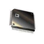
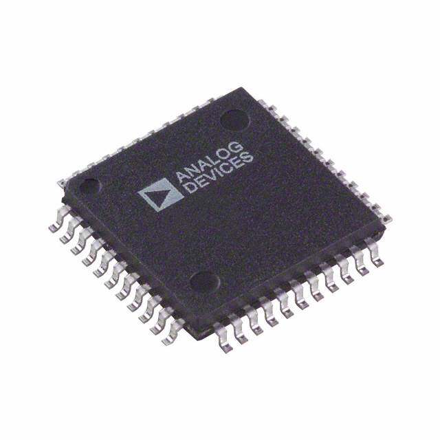
| 供应商器件封装 | 64-LQFP(10x10) |
| 信噪比 | 101 dB |
| 分辨率 | 18 bit |
| 分辨率(位) | 18 b |
| 包装 | 托盘 |
| 商标 | Analog Devices |
| 安装类型 | 表面贴装 |
| 安装风格 | SMD/SMT |
| 封装 | Tray |
| 封装/外壳 | 64-LQFP |
| 封装/箱体 | LQFP-64 |
| 工作温度 | -40°C ~ 85°C |
| 工作电源电压 | 5 V |
| 工厂包装数量 | 160 |
| 接口类型 | Parallel, Serial (SPI, QSPI, Microwire) |
| 数据接口 | DSP,MICROWIRE™,并联,QSPI™,串行,SPI™ |
| 最大功率耗散 | 100 mW |
| 最大工作温度 | + 85 C |
| 最小工作温度 | - 40 C |
| 标准包装 | 1 |
| 特色产品 | http://www.digikey.com/product-highlights/cn/zh/analog-devices-ad-converters/1396 |
| 电压-电源 | 2.3 V ~ 5 V,4.75 V ~ 5.25 V |
| 电压参考 | Internal, External |
| 电压源 | 模拟和数字 |
| 类型 | 数据采集系统(DAS),ADC |
| 系列 | AD7609 |
| 结构 | SAR |
| 转换器数量 | 1 |
| 转换速率 | 200 kS/s |
| 输入类型 | Differential |
| 通道数量 | 8 Channel |
| 采样率(每秒) | 200k |


- 商务部:美国ITC正式对集成电路等产品启动337调查
- 曝三星4nm工艺存在良率问题 高通将骁龙8 Gen1或转产台积电
- 太阳诱电将投资9.5亿元在常州建新厂生产MLCC 预计2023年完工
- 英特尔发布欧洲新工厂建设计划 深化IDM 2.0 战略
- 台积电先进制程称霸业界 有大客户加持明年业绩稳了
- 达到5530亿美元!SIA预计今年全球半导体销售额将创下新高
- 英特尔拟将自动驾驶子公司Mobileye上市 估值或超500亿美元
- 三星加码芯片和SET,合并消费电子和移动部门,撤换高东真等 CEO
- 三星电子宣布重大人事变动 还合并消费电子和移动部门
- 海关总署:前11个月进口集成电路产品价值2.52万亿元 增长14.8%


PDF Datasheet 数据手册内容提取
8-Channel Differential DAS with 18-Bit, Bipolar, Simultaneous Sampling ADC Data Sheet AD7609 FEATURES APPLICATIONS 8 simultaneously sampled inputs Power line monitoring and protection systems True differential inputs Multiphase motor control True bipolar analog input ranges: ±10 V, ±5 V Instrumentation and control systems Single 5 V analog supply and 2.3 V to 5.25 V V Multiaxis positioning systems DRIVE Fully integrated data acquisition solution Data acquisition systems (DAS) Analog input clamp protection COMPANION PRODUCTS Input buffer with 1 MΩ analog input impedance Second-order antialiasing analog filter External References: ADR421, ADR431 On-chip accurate reference and reference buffer Digital Isolators: ADuM1402, ADuM5000, ADuM5402 18-bit ADC with 200 kSPS on all channels Power: ADIsimPower, Supervisor Parametric Search Oversampling capability with digital filter Additional companion products on the AD7609 product page Flexible parallel/serial interface Table 1. High Resolution, Bipolar Input, Simultaneous SPI/QSPI™/MICROWIRE™/DSP compatible Sampling DAS Solutions Performance Single- True Number of 7 kV ESD rating on analog input channels Ended Differential Simultaneous 98 dB SNR, −107 dB THD Resolution Inputs Inputs Sampling Channels Dynamic range: up to 105 dB typical 18 Bits AD7608 AD76091 8 Low power: 100 mW 16 Bits AD7606 8 Standby mode: 25 mW AD7606-6 6 64-lead LQFP package AD7606-4 4 14 Bits AD7607 8 1 Protected by U.S. Patent Number 8,072,360. FUNCTIONAL BLOCK DIAGRAM AVCC AVCC REGCAP REGCAP REFCAPB REFCAPA V1+ CLAMP1MΩ RFB V1– CLAMP1MΩ RFB OSREDCEORN LDP-F T/H L2.D5OV L2.D5OV V2+ CLAMP1MΩ RFB REFIN/REFOUT V2– CLAMP1MΩ RFB OSREDCEORN LDP-F T/H 2.5V REF SELECT V3+ CLAMP1MΩ RFB REF AGND V3– CLAMP1MΩ RFB OSREDCEORN LDP-F T/H OOSS 21 OS 0 V4+ CLAMP1MΩ RFB V4– CLAMP1MΩ RFB OSREDCEORN LDP-F T/H 8:1 SERIAL DDOOUUTTAB VV55+– CCLLAAMMPP11MMΩΩ RRFFBB OSREDCEORN LDP-F T/H MUX 1S8-ABRIT DFIIGLTITEARL IPNATSREEARRLFIALAELCLE/ RCPASDR/S/SCELKR SEL V6+ CLAMP1MΩ RFB VDRIVE V6– CLAMP1MΩ RFB OSREDCEORN LDP-F T/H PARALLEL DB[15:0] AD7609 V7+ CLAMP1MΩ RFB V7– CLAMP1MΩ RFB OSREDCEORN LDP-F T/H CLK OSC V8+ CLAMP 1MΩ RFB CONTROL BUSY V8– CLAMP1MΩ RFB OSRAEDGCENORND LDP-F T/H CONVST ACONIVNSPTU BTSRESETRANGE FRSTDATA 09760-001 Figure 1. Rev. C Document Feedback Information furnished by Analog Devices is believed to be accurate and reliable. However, no responsibility is assumed by Analog Devices for its use, nor for any infringements of patents or other One Technology Way, P.O. Box 9106, Norwood, MA 02062-9106, U.S.A. rights of third parties that may result from its use. Specifications subject to change without notice. No license is granted by implication or otherwise under any patent or patent rights of Analog Devices. Tel: 781.329.4700 ©2011–2018 Analog Devices, Inc. All rights reserved. Trademarks and registered trademarks are the property of their respective owners. Technical Support www.analog.com
AD7609 Data Sheet TABLE OF CONTENTS Features .............................................................................................. 1 Converter Details ....................................................................... 21 Applications ....................................................................................... 1 Analog Input ............................................................................... 21 Companion Products ....................................................................... 1 ADC Transfer Function ............................................................. 22 Functional Block Diagram .............................................................. 1 Internal/External Reference ...................................................... 23 Revision History ............................................................................... 2 Typical Connection Diagram ................................................... 24 General Description ......................................................................... 3 Power-Down Modes .................................................................. 24 Specifications ..................................................................................... 4 Conversion Control ................................................................... 25 Timing Specifications .................................................................. 7 Digital Interface .............................................................................. 26 Absolute Maximum Ratings .......................................................... 11 Parallel Interface (PAR/SER SEL = 0) ...................................... 26 Thermal Resistance .................................................................... 11 Serial Interface (PAR/SER SEL = 1) ......................................... 26 ESD Caution ................................................................................ 11 Reading During Conversion ..................................................... 27 Pin Configuration and Function Descriptions ........................... 12 Digital Filter ................................................................................ 28 Typical Performance Characteristics ........................................... 15 Layout Guidelines....................................................................... 32 Terminology .................................................................................... 19 Outline Dimensions ....................................................................... 34 Theory of Operation ...................................................................... 21 Ordering Guide .......................................................................... 34 REVISION HISTORY 5/2018—Rev. B to Rev. C Changes to Figure 39 and Figure 40............................................. 23 Changes to Patent Note, Note 1 ...................................................... 1 Change to t Parameter, Table 3 ................................................ 7 2/2012—Rev. 0 to Rev. A CONV Changes to Analog Input Ranges Section ................................... 21 5/2014—Rev. A to Rev. B Changes to Patent Footnote ............................................................ 1 7/2011—Revision 0: Initial Version Changes to Figure 37 ...................................................................... 22 Rev. C | Page 2 of 36
Data Sheet AD7609 GENERAL DESCRIPTION The AD7609 is an 18-bit, 8-channel, true differential, The AD7609 operates from a single 5 V supply and can simultaneous sampling analog-to-digital data acquisition accommodate ±10 V and ±5 V true bipolar differential input system (DAS). The part contains analog input clamp protection, signals while sampling at throughput rates up to 200 kSPS for a second-order antialiasing filter, a track-and-hold amplifier, an all channels. The input clamp protection circuitry can tolerate 18-bit charge redistribution successive approximation analog- voltages up to ±16.5 V. The AD7609 has 1 MΩ analog input to-digital converter (ADC), a flexible digital filter, a 2.5 V impedance regardless of sampling frequency. The single supply reference and reference buffer, and high speed serial and operation, on-chip filtering, and high input impedance elimi- parallel interfaces. nate the need for driver op amps and external bipolar supplies. The AD7609 antialiasing filter has a −3 dB cutoff frequency of 32 kHz and provides 40 dB antialias rejection when sampling at 200 kSPS. The flexible digital filter is pin driven, yields improvements in SNR, and reduces the −3 dB bandwidth. Rev. C | Page 3 of 36
AD7609 Data Sheet SPECIFICATIONS V = 2.5 V external/internal, AV = 4.75 V to 5.25 V, V = 2.3 V to 5.25 V; f = 200 kSPS, T = T to T , unless otherwise REF CC DRIVE SAMPLE A MIN MAX noted.1 Table 2. Parameter Test Conditions/Comments Min Typ Max Unit DYNAMIC PERFORMANCE f = 1 kHz sine wave unless otherwise noted IN Signal-to-Noise Ratio (SNR)2, 3 Oversampling by 16; ±10 V range; f = 160 Hz 98 101 dB IN Oversampling by 16; ±5 V range; f = 160 Hz 100 dB IN No oversampling; ±10 V range 90 91 dB No oversampling; ±5 V range 89.5 90.5 dB Signal-to-(Noise + Distortion) (SINAD)2 No oversampling; ±10 V range 89.5 91 dB No oversampling; ±5 V range 89 90 dB Dynamic Range No oversampling; ±10 V range 91.5 dB No oversampling; ±5 V range 90.5 dB Total Harmonic Distortion (THD)2, 3 No oversampling; ±10 V range −107 −97 dB No oversampling; ±5 V range −110 −96 dB Peak Harmonic or Spurious Noise (SFDR)2 −108 dB Intermodulation Distortion (IMD)2 fa = 1 kHz, fb = 1.1 kHz Second-Order Terms −110 dB Third-Order Terms −106 dB Channel-to-Channel Isolation2 f on unselected channels up to 160 kHz −95 dB IN ANALOG INPUT FILTER Full Power Bandwidth −3 dB, ±10 V range 32 kHz −3 dB, ±5 V range 23 kHz −0.1 dB, ±10 V range 13 kHz −0.1 dB, ±5 V range 10 kHz t ±10 V range 7.1 µs GROUP DELAY ±5 V range 10.2 µs DC ACCURACY Resolution No missing codes 18 Bits Differential Nonlinearity2 ±0.75 −0.99/+2 LSB4 Integral Nonlinearity2 ±3 ±7.5 LSB Total Unadjusted Error (TUE) ±10 V range ±10 LSB ±5 V range ±90 LSB Positive Full-Scale Error2, 5 External reference ±8 ±140 LSB Internal reference ±40 LSB Positive Full-Scale Error Drift External reference ±2 ppm/°C Internal reference ±7 ppm/°C Positive Full-Scale Error Matching2 ±10 V range 12 80 LSB ±5 V range 40 100 LSB Bipolar Zero Code Error2, 6 ±10 V range ±3 ±24 LSB ± 5 V range ±3 ±48 LSB Bipolar Zero Code Error Drift ±10 V range 10 µV/°C ± 5 V range 5 µV/°C Bipolar Zero Code Error Matching2 ±10 V range 2.7 30 LSB ±5 V range 13 65 LSB Negative Full-Scale Error2, 5 External reference ±8 ±140 LSB Internal reference ±40 LSB Negative Full-Scale Error Drift External reference ±4 ppm/°C Internal reference ±8 ppm/°C Negative Full-Scale Error Matching2 ±10 V range 12 80 LSB ±5 V range 40 100 LSB Rev. C | Page 4 of 36
Data Sheet AD7609 Parameter Test Conditions/Comments Min Typ Max Unit ANALOG INPUT Differential Input Voltage Ranges VIN = Vx+ − (Vx−) RANGE = 1; ±10 V −20 +20 V RANGE = 0; ±5 V −10 +10 V Absolute Voltage Input ±10 V range, see the Analog Input Clamp −10 +10 V Protection section ±5 V range, see the Analog Input Clamp −5 +5 V Protection section Common-Mode Input Range −4 ±5 +4 V CMRR −70 dB Analog Input Current 10 V, see Figure 28 5.4 µA 5 V, see Figure 28 2.5 µA Input Capacitance7 5 pF Input Impedance 1 MΩ REFERENCE INPUT/OUTPUT Reference Input Voltage Range 2.475 2.5 2.525 V DC Leakage Current ±1 µA Input Capacitance7 REF SELECT = 1 7.5 pF Reference Output Voltage REFIN/REFOUT 2.49/ V 2.505 Reference Temperature Coefficient ±10 ppm/°C LOGIC INPUTS Input High Voltage (V ) 0.7 × V V INH DRIVE Input Low Voltage (V ) 0.3 × V V INL DRIVE Input Current (I ) ±2 µA IN Input Capacitance (C )7 5 pF IN LOGIC OUTPUTS Output High Voltage (V ) I = 100 µA V − 0.2 V OH SOURCE DRIVE Output Low Voltage (V ) I = 100 µA 0.2 V OL SINK Floating-State Leakage Current ±1 ±20 µA Floating-State Output Capacitance7 5 pF Output Coding Twos complement CONVERSION RATE Conversion Time All eight channels included 4 µs Track-and-Hold Acquisition Time 1 µs Throughput Rate Per channel, all eight channels included 200 kSPS POWER REQUIREMENTS AV 4.75 5.25 V CC V 2.3 5.25 V DRIVE I Digital inputs = 0 V or V TOTAL DRIVE Normal Mode (Static) 16 22 mA Normal Mode (Operational)8 f = 200 kSPS 20 28.5 mA SAMPLE Standby Mode 5 8 mA Shutdown Mode 2 11 µA Rev. C | Page 5 of 36
AD7609 Data Sheet Parameter Test Conditions/Comments Min Typ Max Unit Power Dissipation Normal Mode (Static) 80 115.5 mW Normal Mode (Operational)8 f = 200 kSPS 100 157 mW SAMPLE Standby Mode 25 42 mW Shutdown Mode 10 60.5 µW 1 Temperature range for B version is −40°C to +85°C. 2 See the Terminology section. 3 This specification applies when reading during a conversion or after a conversion. If reading during a conversion in parallel and serial modes with VDRIVE = 5 V, SNR typically reduces by 1.5 dB and THD by 3 dB. 4 LSB means least significant bit. With ±5 V input range, 1 LSB = 76.29 µV. With ±10 V input range, 1 LSB = 152.58 µV. 5 These specifications include the full temperature range variation and contribution from the internal reference buffer but do not include the error contribution from the external reference. 6 Bipolar zero code error is calculated with respect to the analog input voltage. See the Analog Input Clamp Protection section. 7 Sample tested during initial release to ensure compliance. 8 Operational power/current figure includes contribution when running in oversampling mode. Rev. C | Page 6 of 36
Data Sheet AD7609 TIMING SPECIFICATIONS AV = 4.75 V to 5.25 V, V = 2.3 V to 5.25 V, V = 2.5 V external reference/ internal reference, T = T to T , CC DRIVE REF A MIN MAX unless otherwise noted.1 Table 3. Limit at T , T MIN MAX Parameter Min Typ Max Unit Description PARALLEL/SERIAL/BYTE MODE t 1/throughput rate CYCLE 5 µs Parallel mode, reading during; or after conversion V = 2.7 V to 5.25 V; or DRIVE serial mode: V = 3.3 V to 5.25 V, reading during a conversion using D A DRIVE OUT and D B lines OUT 5 µs Parallel mode reading after conversion V = 2.3 V DRIVE 10.1 µs Serial mode reading after conversion; V = 2.7 V, D A and D B lines DRIVE OUT OUT 11.5 µs Serial mode reading after a conversion; V = 2.3 V, D A and D B lines DRIVE OUT OUT t Conversion time CONV 3.45 4 4.2 µs Oversampling off 7.87 9.1 µs Oversampling by 2 16.05 18.8 µs Oversampling by 4 33 39 µs Oversampling by 8 66 78 µs Oversampling by 16 133 158 µs Oversampling by 32 257 315 µs Oversampling by 64 t 100 µs STBY rising edge to CONVST x rising edge; power-up time from standby mode WAKE-UP STANDBY t WAKE-UP SHUTDOWN Internal Reference 30 ms STBY rising edge to CONVST x rising edge; power-up time from shutdown mode External Reference 13 ms STBY rising edge to CONVST x rising edge; power-up time from shutdown mode t 50 ns RESET high pulse width RESET t 20 ns BUSY to OS x pin setup time OS_SETUP t 20 ns BUSY to OS x pin hold time OS_HOLD t 45 ns CONVST x high to BUSY high 1 t 25 ns Minimum CONVST x low pulse 2 t 25 ns Minimum CONVST x high pulse 3 t 0 ns BUSY falling edge to CS falling edge setup time 4 t2 0.5 ms Maximum delay allowed between CONVST A, CONVST B rising edges 5 t 25 ns Maximum time between last CS rising edge and BUSY falling edge 6 t 25 ns Minimum delay between RESET low to CONVST x high 7 PARALLEL READ OPERATION t 0 ns CS to RD setup time 8 t 0 ns CS to RD hold time 9 t RD low pulse width 10 19 ns V above 4.75 V DRIVE 24 ns V above 3.3 V DRIVE 30 ns V above 2.7 V DRIVE 37 ns V above 2.3 V DRIVE t 15 ns RD high pulse width 11 t 22 ns CS high pulse width (see Figure 5); CS and RD linked 12 Rev. C | Page 7 of 36
AD7609 Data Sheet Limit at T , T MIN MAX Parameter Min Typ Max Unit Description t Delay from CS until DB[15:0] three-state disabled 13 19 ns V above 4.75 V DRIVE 24 ns V above 3.3 V DRIVE 30 ns V above 2.7 V DRIVE 37 ns V above 2.3 V DRIVE t 3 Data access time after RD falling edge 14 19 ns V above 4.75 V DRIVE 24 ns V above 3.3 V DRIVE 30 ns V above 2.7 V DRIVE 37 ns V above 2.3 V DRIVE t 6 ns Data hold time after RD falling edge 15 t 6 ns CS to DB[15:0] hold time 16 t 22 ns Delay from CS rising edge to DB[15:0] three-state enabled 17 SERIAL READ OPERATION f Frequency of serial read clock SCLK 20 MHz V above 4.75 V DRIVE 15 MHz V above 3.3 V DRIVE 12.5 MHz V above 2.7 V DRIVE 10 MHz V above 2.3 V DRIVE t Delay from CS until D A/D B three-state disabled/delay from CS until 18 OUT OUT MSB valid 18 ns V above 4.75 V DRIVE 23 ns V above 3.3 V DRIVE 35 ns V = 2.3 V to 2.7 V DRIVE t 3 Data access time after SCLK rising edge 19 20 ns V above 4.75 V DRIVE 26 ns V above 3.3 V DRIVE 32 ns V above 2.7 V DRIVE 39 ns V above 2.3 V DRIVE t 0.4 t ns SCLK low pulse width 20 SCLK t 0.4 t ns SCLK high pulse width 21 SCLK t 7 SCLK rising edge to D A/D B valid hold time 22 OUT OUT t 22 ns CS rising edge to D A/D B three-state enabled 23 OUT OUT FRSTDATA OPERATION t Delay from CS falling edge until FRSTDATA three-state disabled 24 18 ns V above 4.75 V DRIVE 23 ns V above 3.3 V DRIVE 30 ns V above 2.7 V DRIVE 35 ns V above 2.3 V DRIVE t ns Delay from CS falling edge until FRSTDATA high, serial mode 25 18 ns V above 4.75 V DRIVE 23 ns V above 3.3 V DRIVE 30 ns V above 2.7 V DRIVE 35 ns V above 2.3 V DRIVE t Delay from RD falling edge to FRSTDATA high 26 19 ns V above 4.75 V DRIVE 23 ns V above 3.3 V DRIVE 30 ns V above 2.7 V DRIVE 35 ns V above 2.3 V DRIVE Rev. C | Page 8 of 36
Data Sheet AD7609 Limit at T , T MIN MAX Parameter Min Typ Max Unit Description t Delay from RD falling edge to FRSTDATA low 27 22 ns V = 3.3 V to 5.25 V DRIVE 29 ns V = 2.3 V to 2.7 V DRIVE t Delay from 18th SCLK falling edge to FRSTDATA low 28 20 ns V = 3.3 V to 5.25 V DRIVE 27 ns V = 2.3 V to 2.7 V DRIVE t 29 ns Delay from CS rising edge until FRSTDATA three-state enabled 29 1 Sample tested during initial release to ensure compliance. All input signals are specified with tR = tF = 5 ns (30% to 70% of VDD) and timed from a voltage level of 1.6 V. 2 The delay between the CONVST x signals was measured as the maximum time allowed while ensuring a <40 LSB performance matching between channel sets. 3 A buffer is used on the data output pins for these measurements, which is equivalent to a load of 20 pF on the output pins. Timing Diagrams t5 CONVST A/ CONVST B tCYCLE t2 CONVST A/ CONVST B t3 tCONV t1 BUSY t4 CS t7 RESET tRESET 09760-002 Figure 2. CONVST x Timing—Reading After a Conversion t5 CONVST A/ CONVST B tCYCLE t2 CONVST A/ CONVST B t3 tCONV t1 BUSY t6 CS t7 RESET tRESET 09760-003 Figure 3. CONVST x Timing—Reading During a Conversion CS t9 t8 t10 t11 RD t16 t13 t14 t15 t17 DATA: V1 V1 V2 V2 V8 V8 DB[15:0] INVALID [17:2] [1:0] [17:2] [1:0] [17:2] [1:0] FRSTDATA t24 t26 t27 t29 09760-004 Figure 4. Parallel Mode Separate CS and RD Pulses Rev. C | Page 9 of 36
AD7609 Data Sheet t12 CS, RD t13 t16 t17 DATA: V1 V1 V2 V2 V7 V7 V8 V8 DB[15:0] [17:2] [1:0] [17:2] [1:0] [17:2] [1:0] [17:2] [1:0] FRSTDATA 09760-005 Figure 5. CS and RD Linked Parallel Mode CS SCLK t21 t20 t18 t19 t22 t23 DDOOUUTTAB, DB17 DB14 DB13 DB1 DB0 t25 t28 t29 FRSTDATA 09760-006 Figure 6. Serial Read Operation Rev. C | Page 10 of 36
Data Sheet AD7609 ABSOLUTE MAXIMUM RATINGS T = 25°C, unless otherwise noted. THERMAL RESISTANCE A θ is specified for the worst-case conditions, that is, a device Table 4. JA soldered in a circuit board for surface-mount packages. These Parameter Rating specifications apply to a 4-layer board. AV to AGND −0.3 V to +7 V CC V to AGND −0.3 V to AV + 0.3 V DRIVE CC Table 5. Thermal Resistance Analog Input Voltage to AGND1 ±16.5 V Package Type θ θ Unit JA JC Digital Input Voltage to AGND −0.3 V to V + 0.3 V DRIVE 64-Lead LQFP 45 11 °C/W Digital Output Voltage to AGND −0.3 V to V + 0.3 V DRIVE REFIN to AGND −0.3 V to AV + 0.3 V CC Input Current to Any Pin Except ±10 mA ESD CAUTION Supplies1 Operating Temperature Range B Version −40°C to +85°C Storage Temperature Range −65°C to +150°C Junction Temperature 150°C Pb/SN Temperature, Soldering Reflow (10 sec to 30 sec) 240(+0)°C Pb-Free Temperature, Soldering Reflow 260(+0)°C ESD (All Pins Except Analog Inputs) 2 kV ESD (Analog Input Pins Only) 7 kV 1 Transient currents of up to 100 mA do not cause SCR latch-up. Stresses at or above those listed under Absolute Maximum Ratings may cause permanent damage to the product. This is a stress rating only; functional operation of the product at these or any other conditions above those indicated in the operational section of this specification is not implied. Operation beyond the maximum operating conditions for extended periods may affect product reliability. Rev. C | Page 11 of 36
AD7609 Data Sheet PIN CONFIGURATION AND FUNCTION DESCRIPTIONS – + – + – + – + – + – + – + – + 8 8 7 7 6 6 5 5 4 4 3 3 2 2 1 1 V V V V V V V V V V V V V V V V 64 63 62 61 60 59 58 57 56 55 54 53 52 51 50 49 AVCC 1 48 AVCC ANALOG INPUT AGND 2 PIN 1 47 AGND DECOUPLING CAPACITOR PIN OS 0 3 46 REFGND POWER SUPPLY OS 1 4 45 REFCAPB GROUND PIN OS 2 5 44 REFCAPA DATA OUTPUT PAR/SER SEL 6 AD7609 43 REFGND DIGITAL OUTPUT STBY 7 TOP VIEW 42 REFIN/REFOUT DIGITAL INPUT RANGE 8 (Not to Scale) 41 AGND CONVST A 9 40 AGND REFERENCE INPUT/OUTPUT CONVST B 10 39 REGCAP RESET 11 38 AVCC RD/SCLK 12 37 AVCC CS 13 36 REGCAP BUSY 14 35 AGND FRSTDATA 15 34 REF SELECT DB0 16 33 DB15 17 18 19 20 21 22 23 24 25 26 27 28 29 30 31 32 1 2 3 4 5 6 EA B D 9 0 1 2 3 4 DB DB DB DB DB DB VDRIVDB7/DOUTDB8/DOUT AGN DB DB1 DB1 DB1 DB1 DB1 09760-007 Figure 7. Pin Configuration Table 6. Pin Function Descriptions Pin No. Type1 Mnemonic Description 1, 37, 38, 48 P AV Analog Supply Voltage 4.75 V to 5.25 V. This supply voltage is applied to the internal front-end CC amplifiers and to the ADC core. These supply pins should be decoupled to AGND. 2, 26, 35, P AGND Analog Ground. This pin is the ground reference point for all analog circuitry on the AD7609. All 40, 41, 47 analog input signals and external reference signals should be referred to these pins. All six of these AGND pins should connect to the AGND plane of a system. 23 P V Logic Power Supply Input. The voltage (2.3 V to 5 V) supplied at this pin determines the operating DRIVE voltage of the interface. This pin is nominally at the same supply as the supply of the host interface (that is, DSP, FPGA). 36, 39 P REGCAP Decoupling Capacitor Pins for Voltage Output from Internal Regulator. These output pins should be decoupled separately to AGND using a 1 μF capacitor. The voltage on these output pins is in the range of 2.5 V to 2.7 V. 49, 51, 53, AI+ V1+ to V8+ Analog Input V1+ to Analog Input V8+. These pins are the positive terminal of the true differential 55, 57, 59, analog inputs. The analog input range of these channels is determined by the RANGE pin. 61, 63 50, 52, 54, AI− V1− to V8− Analog Input V1− to Analog Input V8−. These are the negative terminals of the true differential 56, 58, 60, analog inputs. The analog input range of these channels is determined by the RANGE pin. The signal 62, 64 on this pin should be 180° out of phase with the corresponding Vx+ pin. 42 REF REFIN/ Reference Input/ Reference Output. The on-chip reference of 2.5 V is available on this pin for external REFOUT use if the REF SELECT pin is set to a logic high. Alternatively, the internal reference can be disabled by setting the REF SELECT pin to a logic low and an external reference of 2.5 V can be applied to this input. See the Internal/External Reference section. Decoupling is required on this pin for both the internal or external reference options. A 10 µF capacitor should be applied from this pin to ground close to the REFGND pins. 34 DI REF SELECT Internal/External Reference Selection Input. Logic input. If this pin is set to logic high, the internal reference is selected and is enabled. If this pin is set to logic low, the internal reference is disabled and an external reference voltage must be applied to the REFIN/REFOUT pin. 44, 45 REF REFCAPA, Reference Buffer Output Force/Sense Pins. These pins must be connected together and decoupled to REFCAPB AGND using a low ESR 10 μF ceramic capacitor. 43, 46 REF REFGND Reference Ground Pins. These pins should be connected to AGND. Rev. C | Page 12 of 36
Data Sheet AD7609 Pin No. Type1 Mnemonic Description 8 DI RANGE Analog Input Range Selection. Logic input. The polarity on this pin determines the input range of the analog input channels. If this pin is tied to a logic high, the analog input range is ±10 V for all channels. If this pin is tied to a logic low, the analog input range is ±5 V for all channels. A logic change on this pin has an immediate effect on the analog input range. Changing this pin during a conversion is not recommended. See the Analog Input section for more details. 6 DI PAR/ Parallel/Serial Interface Selection Input. Logic input. If this pin is tied to a logic low, the parallel SER SEL interface is selected. If this pin is tied to a logic high, the serial interface is selected. In serial mode, the RD/SCLK pin functions as the serial clock input. The DB7/D A and DB8/D B pins OUT OUT function as serial data outputs. When the serial interface is selected, the DB[15:9] and DB[6:0] pins should be tied to AGND. 9, 10 DI CONVST A, Conversion Start Input A, Conversion Start Input B. Logic inputs. These logic inputs are used to initiate CONVST B conversions on the analog input channels. For simultaneous sampling of all input channels, CONVST A and CONVST B can be shorted together and a single conversion start signal applied. Alternatively, CONVST A can be used to initiate simultaneous sampling for V1, V2, V3, and V4, and CONVST B can be used to initiate simultaneous sampling on the other analog inputs (V5, V6, V7, and V8). This is only possible when oversampling is not switched on. When the CONVST A or CONVST B pin transitions from low to high, the front-end track-and-hold circuitry for their respective analog inputs is set to hold. This function allows a phase delay to be created inherently between the sets of analog inputs. 13 DI CS Chip Select. This active low logic input frames the data transfer. When both CS and RD are logic low in parallel mode, the output bus (DB[15:0]) is enabled and the conversion result is output on the parallel data bus lines. In serial mode, the CS is used to frame the serial read transfer and clocks out the MSB of the serial output data. 12 DI RD/SCLK Parallel Data Read Control Input When Parallel Interface is Selected (RD)/Serial Clock Input When Serial Interface is Selected (SCLK). When both CS and RD are logic low in parallel mode, the output bus is enabled. In parallel mode, two RD pulses are required to read the full 18 bits of conversion results from each channel. The first RD pulse outputs DB[17:2], and the second RD pulses outputs DB[1:0]. In serial mode, this pin acts as the serial clock input for data transfers. The CS falling edge takes the data output lines, D A and D B, out of three-state and clocks out the MSB of the OUT OUT conversion result. The rising edge of SCLK clocks all subsequent data bits onto the serial data outputs, D A and D B. For further information, see the Conversion Control section. OUT OUT 14 DO BUSY Busy Output. This pin transitions to a logic high after both CONVST A and CONVST B rising edges and indicates that the conversion process has started. The BUSY output remains high until the conversion process for all channels is complete. The falling edge of BUSY signals that the conversion data is being latched into the output data registers and will be available to be read after a time, t. Any data read 4 while BUSY is high should be complete before the falling edge of BUSY occurs. Rising edges on CONVST A or CONVST B have no effect while the BUSY signal is high. 11 DI RESET Reset Input. When set to logic high, the rising edge of RESET resets the AD7609. The part must receive a RESET pulse after power-up. To achieve the specified performance after the RESET signal, the t WAKE_UP time should elapse between power-on and the RESET pulse. The RESET high pulse should be SHUTDOWN typically 100 ns wide. If a RESET pulse is applied during a conversion, the conversion is aborted. If a RESET pulse is applied during a read, the contents of the output registers reset to all zeros. 15 DO FRSTDATA Digital Output. The FRSTDATA output signal indicates when the first channel, V1, is being read back on either the parallel or serial interface. When the CS input is high, the FRSTDATA output pin is in three-state. The falling edge of CS takes FRSTDATA out of three-state. In parallel mode, the falling edge of RD corresponding to the result of V1 then sets the FRSTDATA pin high, indicating that the result from V1 is available on the output data bus. The FRSTDATA output returns to a logic low following the third falling edge of RD. In serial mode, FRSTDATA goes high on the falling edge of CS as this clocks out the MSB of V1 on DOUTA. It returns low on the 18th SCLK falling edge after the CS falling edge. See the Conversion Control section for more details. 7 DI STBY Standby Mode Input. This pin is used to place the AD7609 into one of two power-down modes: standby mode or shutdown mode. The power-down mode entered depends on the state of the RANGE pin, as shown in Table 8. When in standby mode, all circuitry except the on-chip reference, regulators, and regulator buffers is powered down. When in shutdown mode, all circuitry is powered down. Rev. C | Page 13 of 36
AD7609 Data Sheet Pin No. Type1 Mnemonic Description 5, 4, 3 DI OS [2:0] Oversampling Mode Pins. Logic inputs. These inputs are used to select the oversampling ratio. OS 2 is the MSB control bit, and OS 0 is the LSB control bit. See the Digital Filter section for additional details on the oversampling mode of operation and Table 9 for oversampling bit decoding. 33 DO/DI DB15 Parallel Output Data Bits, Data Bit 15. When PAR/SER SEL = 0, this pin acts as three-state parallel digital output pin. This pin is used to output DB17 of the conversion result during the first RD pulse and DB1 of the same conversion result during the second RD pulse. When PAR/SER SEL = 1, this pin should be tied to AGND. 32 DO/DI DB14 Parallel Output Data Bits, Data Bit 14. When PAR/SER SEL = 0, this pin acts as three-state parallel digital output pin. When CS and RD are low, this pin is used to output DB16 of the conversion result during the first RD pulse and DB0 of the same conversion result during the second RD pulse. When PAR/SER SEL = 1, this pin should be tied to AGND. 31 to 27 DO DB[13:9] Parallel Output Data Bits, Data Bit 13 to Data Bit 9. When PAR/SER SEL = 0, these pins act as three-state parallel digital input/output pins. When CS and RD are low, these pins are used to output DB15 to DB11 of the conversion result during the first RD pulse and output 0 during the second RD pulse. When PAR/SER SEL = 1, these pins should be tied to AGND. 24 DO DB7/D A Parallel Output Data Bit 7 (DB7)/Serial Interface Data Output Pin (D A). When PAR/SER SEL = 0, this OUT OUT pins acts as a three-state parallel digital input/output pin. When CS and RD are low, this pin is used to output DB9 of the conversion result. When PAR/SER SEL = 1, this pin functions as D A and outputs OUT serial conversion data. See the Conversion Control section for further details. 25 DO DB8/D B Parallel Output Data Bit 8 (DB8)/Serial Interface Data Output Pin (D B). When PAR/SER SEL = 0, this OUT OUT pins acts as a three-state parallel digital input/output pin. When CS and RD are low, this pin is used to output DB10 of the conversion result. When PAR/SER SEL = 1, this pin functions as D B and outputs OUT serial conversion data. See the Conversion Control section for further details. 22 to 16 DO DB[6:0] Parallel Output Data Bits, Data Bit 6 to Data Bit 0. When PAR/SER SEL = 0, these pins act as three-state parallel digital input/output pins. When CS and RD are low, these pins are used to output DB8 to DB2 of the conversion result during the first RD pulse and output 0 during the second RD pulse. When PAR/SER SEL = 1, these pins should be tied to AGND. 1 Refers to classification of pin type; P denotes power, AI denotes analog input, REF denotes reference, DI denotes digital input, DO denotes digital output. Rev. C | Page 14 of 36
Data Sheet AD7609 TYPICAL PERFORMANCE CHARACTERISTICS 3 0 AVCC,VDRIVE=5V 2 –20 INTERNALREFERENCE ±10VRANGE –40 fSAMPLE=200kSPS 1 1fI6N3=841kPHOzINTFFT SB) dB) –60 STHNDR ==–9111.512.0d5BdB NL (L 0 R ( –80 I SN –1 ±10VRANGE –100 AVCC,VDRIVE=5V TA=25°C –2 fSAMPLE=200kSPS –120 WCP INL = 1.69 LSB WCN INL = –1.3 LSB –140 –3 0 8 6 4 2 0 8 6 6 3 0 7 4 0 7 7 5 3 0 8 6 3 –1600 20k INPU4T0 kFREQUEN6C0Yk (Hz) 80k 100k 09760-008 32, 65, 98, CO131,DE 163, 196, 229, 09760-010 Figure 8. FFT Plot, ±10 V Range Figure 11. Typical INL, ±10 V Range 1.0 ±10VRANGE 0 0.8 AVCC,VDRIVE=5V –20 AINVTCECR,NVADRLIVREEF=E5RVENCE 0.6 fTWSAAC=MPP2 DL5NE°CL= =2 000.3k3S LPSSB ±5VRANGE 0.4 WCN DNL = –0.32 LSB –40 fSAMPLE=200kSPS UDE (dB) ––8600 f1ST6HINN,D3R=8 ==41 –kP91H1O0.z1I9N2.7dT7BFdFBT DNL (LSB)–00..220 T LI MP–100 –0.4 A –0.6 –120 –0.8 –140 –1.0 0 8 6 4 2 0 8 6 6 3 0 7 4 0 7 –1600 20k INPU4T0 kFREQUEN6C0Yk (Hz) 80k 100k 09760-009 32,7 65,5 98,3 CO131,0DE 163,8 196,6 229,3 09760-011 Figure 9. FFT Plot, ±5 V Range Figure 12. Typical DNL, ±10 V Range 3 0 AVCC,VDRIVE=5V 2 –20 INTERNALREFERENCE ±10VRANGE –40 fSAMPLE=12.5kSPS 1 DE (dB) –60 f8STI1HNN9 DR=2: 1=P–H O11z10I1N0..T77 41FddFBBT NL (LSB) 0 U –80 I T LI –1 ±5VRANGE P AM–100 AVCC,VDRIVE=5V TA=25°C –120 –2 fSAMPLE=200kSPS WCP INL = 1.56 LSB WCN INL = –1.22 LSB –140 –3 0 8 6 4 2 0 8 6 6 3 0 7 4 0 7 –1600 1 IN2PUT FREQ3UENCY (kH4z) 5 6 09760-109 32,7 65,5 98,3 CO131,0DE 163,8 196,6 229,3 09760-012 Figure 10. FFT Plot, ±10 V Range Figure 13. Typical INL, ±5 V Range Rev. C | Page 15 of 36
AD7609 Data Sheet 1.0 ±5V RANGE 0.8 ATAV C=C 2, 5V°DCRIVE = 5V 40 0.6 fWSACMPP ILNEL = = 2 00.04 5k SLPSSB 32 0.4 WCN INL = –0.38 LSB LSB) 24 PFS ERROR B) 0.2 NG ( 16 DNL (LS –0.20 L MATCHI 08 NFS ERROR E N –0.4 AN –8 H –0.6 S C –16 F –0.8 S/P –24 F –1.00 8 6 4 2 0 8 6 N –32 ±A1V0CVC R, VADNRGIVEE = 5V 32,76 65,53 98,30 CO131,07DE 163,84 196,60 229,37 09760-013 –40–40 –25 –10 T5EMPER20ATURE3E 5(X°CT)ER5N0AL RE6F5EREN8C0E 09760-218 Figure 14. Typical DNL, ±5 V Range Figure 17. NFS and PFS Error Matching 80 10 60 8 40 ±10V RANGE S) B) %F 6 ERROR (LS 200 ±5V RANGE S ERROR ( 4 S –20 NF NF S/ 2 AVCC, VDRIVE = 5V –40 PF fSAMPLE = 200 kSPS TA = 25°C 0 EXTERNAL REFERENCE –60 200kSPS SOURCE RESISTANCE IS MATCHED ON AVCC, VDRIVE = 5V THE V– INPUT EXTERNAL REFERENCE ±10V AND ±5V RANGE –80 –2 –40 –25 –10 T5EMPER20ATURE3 5(°C) 50 65 80 09760-117 0 20k S4O0UkRCE RE6S0kISTANCE8 0(kΩ) 100k 120k 09760-219 Figure 15. NFS Error vs. Temperature Figure 18. PFS and NFS Error vs. Source Resistance 80 105 AVCC,VDRIVE = 5V 60 fSAMPLE CHANGES WITH OS RATE TA = 25°C 100 INTERNAL REFERENCE 40 ±10V RANGE B) S 20 R (L Bs) 95 S ERRO –200 ±5V RANGE SNR (d 90 PF ±10V RANGE NO OS OS × 2 –40 OS × 4 85 OS × 8 –60 200kSPS OS × 16 OS × 32 AVCC, VDRIVE = 5V OS × 64 EXTERNAL REFERENCE –80 80 –40 –25 –10 T5EMPER20ATURE3 5(°C) 50 65 80 09760-118 10 100 INPUT FRE1Q0UkENCY (Hz) 10k 100k 09760-017 Figure 16. PFS Error vs. Temperature Figure 19. SNR vs. Input Frequency, ±10 V Range Rev. C | Page 16 of 36
Data Sheet AD7609 105 8 AVCC,VDRIVE = 5V fSAMPLE CHANGES WITH OS RATE TA = 25°C 6 100 INTERNAL REFERENCE B) ±5V RANGE R (LS 4 O R (dBs) 95 RO ERR 2 SN 90 R ZE 0 ±5V RANGE NO OS LA OS × 2 O –2 85 OOSS ×× 48 BIP ±10V RANGE OS × 16 –4 200 kSPS OS × 32 AVCC,VDRIVE = 5V OS × 64 EXTERNAL REFERENCE 8010 100 INPUT FRE1Q0UkENCY (Hz) 10k 100k 09760-018 –6–40 –20 0TEMPER2A0TURE (°4C0) 60 80 09760-023 Figure 20. SNR vs. Input Frequency, ±5 V Range Figure 23. Bipolar Zero Code Error vs. Temperature –60 ±10VRANGE 16 AVCC,VDRIVE=5V SB) –70 RfTSASAO=MUP2RL5CE°EC= M2A0T0CkHSEPDS HING (L 12 ±5V RANGE –80 ON Vx+, Vx– INPUTS TC 8 A D (dB) –90 ROR M 4 ±10V RANGE TH 1050Ω0Ω0Ω DE ER 0 –100 51k.2ΩkΩ O CO –4 10kΩ R E –8 –110 Z R A L –12 200kSPS –1201 FREQUE1N0CY (kHz) 100 09760-020 BIPO –16–40 –25 –10 T5EMPER20ATURE3EA 5(X°VCTC)EC,R V5N0DARLIV RE E=6F 55EVREN8C0E 09760-224 Figure 21. THD vs. Input Frequency for Various Source Impedances, Figure 24. Bipolar Zero Code Error Matching Between Channels ±10 V Range –50 –40 ±5VRANGE B) –60 AINVTCECR, NVADRLI VREE =F E5RVENCE B) –––765000 RAfTOSASVNAOC= MVUCP2xR,L5+CVE°,E CD = VRMxI2VA–0E T0INC=kPHS5UEPVTDSS EL ISOLATION (d –––789000 fTASADA 7=M6 P20L59E° RC=E 2C0O0kMSMPESNDED DEC±1O0UVP RLAINNGG UESED THD (d –80 0Ω CHANN –100 ±5V RANGE –90 1500Ω0Ω TO- –110 1.2kΩ L- –100 5kΩ NE –120 10kΩ N A H –110 C –130 –1201 FREQUE1N0CY (kHz) 100 09760-019 –1400 20 40 NOIS60E FREQ80UENCY10 (0kHz)120 140 160 09760-225 Figure 22. THD vs. Input Frequency for Various Source Impedances, Figure 25. Channel-to-Channel Isolation ±5 V Range Rev. C | Page 17 of 36
AD7609 Data Sheet 110 22 20 105 A) ±10V RANGE m MIC RANGE (dB) 10905 ±5V RANGE PLY CURRENT ( 111864 DYNA 90 SUPCC 12 85 ATINAVT C=EC R2 =5N °VACDLR RIVEEF =E R5VENCE AV 10 IATNAVT C=EC R2, 5NV°ADCRLI VREE =F E5RVENCE fSAMPLE SCALES WITH OS RATIO fSAMPLE VARIES WITH OS RATE 80 NO OS OS × 2 OOSV E×R 4SAOMSP L×I N8G ORSA T×I O16 OS × 32 OS × 64 09760-023 N8O OS OS × 2 OSO V×E 4RSAOMSP L×I N8G ROAST I×O 16 OS × 32 OS × 64 09760-227 Figure 26. Dynamic Range vs. Oversampling Ratio Figure 29. Supply Current vs. Oversampling Rate 140 2.5010 dB) 130 O ( 2.5005 AVCC = 5V AVCC = 5.25V RATI 120 ±10V RANGE E (V)2.5000 TION 110 AG EC ±5V RANGE VOLT2.4995 Y REJ 100 UT AVCC = 4.75V PL 90 REFO2.4990 R SUP 80 AVCC, VDRIVE = 5V E INTERNAL REFERENCE W 2.4985 PO 70 fASDA7M6P0L9E R=E 2C0O0kMSMPESNDED DECOUPLING USED TA = 25°C 60 2.4980–40 –25 –10 T5EMPER20ATURE3 5(°C) 50 65 80 09760-029 0 100 200 3A0V0CC 4N0O0ISE50 F0RE6Q0U0EN7C00Y (k8H0z0) 900 1000 1100 09760-130 Figure 27. Reference Output Voltage vs. Temperature for Different Supply Figure 30. PSRR Voltages 10 0 AfSVACMCP,L VED =R I2V0E0 =k S5PVS –10 ATfSAVA C=MC P2,L 5VE°D C=R I2V0E0 =kS 5PVS 5 –20 INTERNAL REFERENCE –30 URRENT (µA) –50 CMRR (dB)–––654000 ±5V RANGE C ±10V RANGE –70 +25°C V+ +25°C V– –10 +85°C V– –80 +85°C V+ –40°C V– –90 –40°C V+ –15 –100 –20DIFF–E1R5ENTI–A1L0ANAL–O5G INPU0T VOLTA5GE (V1x0+ – (Vx1–5)) (V)20 09760-025 10 100 FREQUE1kNCY (Hz) 10k 100k09760-028 Figure 28. Analog Input Current vs. Input Voltage Over Temperature Figure 31. CMRR vs. Common-Mode Ripple Frequency Rev. C | Page 18 of 36
Data Sheet AD7609 TERMINOLOGY Integral Nonlinearity Signal-to-(Noise + Distortion) Ratio The maximum deviation from a straight line passing through The measured ratio of signal-to-(noise + distortion) at the the endpoints of the ADC transfer function. The endpoints of output of the ADC. The signal is the rms amplitude of the the transfer function are zero scale, a ½ LSB below the first code fundamental. Noise is the sum of all nonfundamental signals transition, and full scale at ½ LSB above the last code transition. up to half the sampling frequency (f/2, excluding dc). The ratio S depends on the number of quantization levels in the digitization Differential Nonlinearity process: the more levels, the smaller the quantization noise. The The difference between the measured and the ideal 1 LSB theoretical signal-to-(noise + distortion) ratio for an ideal N-bit change between any two adjacent codes in the ADC. converter with a sine wave input is given by Bipolar Zero Code Error Signal-to-(Noise + Distortion) = (6.02 N + 1.76) dB The deviation of the midscale transition (all 1s to all 0s) from the ideal V voltage, that is, AGND. Thus, for an 18-bit converter, this is 110.12 dB. IN Bipolar Zero Code Error Match Total Harmonic Distortion (THD) The difference in bipolar zero code error between any two input The ratio of the rms sum of the harmonics to the fundamental. channels. For the AD7609, it is defined as Positive Full-Scale Error THD (dB) = The last transition (from 011 . . . 10 to 011 . . . 11 in twos V 2+V 2+V 2+V 2+V 2+V 2+V 2+V 2 complement coding) should occur for an analog voltage 1½ 20log 2 3 4 5 6 7 8 9 V LSB below the nominal full scale (9.99977 V for the ±10 V 1 range and 4.99988 V for the ±5 V range). The positive full-scale where: error is the deviation of the actual level of the last transition V is the rms amplitude of the fundamental. 1 from the ideal level. V to V are the rms amplitudes of the second through ninth 2 9 Positive Full-Scale Error Match harmonics. The difference in positive full-scale error between any two input Peak Harmonic or Spurious Noise channels. The ratio of the rms value of the next largest component in the Negative Full-Scale Error ADC output spectrum (up to fS/2, excluding dc) to the rms value The first transition (from 100 . . . 00 to 100 . . . 01 in twos of the fundamental. Normally, the value of this specification is complement coding) should occur for an analog voltage ½ LSB determined by the largest harmonic in the spectrum, but for above the negative full scale (−9.999923 V for the ±10 V range ADCs where the harmonics are buried in the noise floor, it is and −4.9999618 for the ±5 V range). The negative full-scale determined by a noise peak. error is the deviation of the actual level of the first transition Intermodulation Distortion from the ideal level. With inputs consisting of sine waves at two frequencies, fa and fb, Negative Full-Scale Error Match any active device with nonlinearities creates distortion products The difference in negative full-scale error between any two at sum and difference frequencies of mfa ± nfb, where m, n = 0, input channels. 1, 2, 3. Intermodulation distortion terms are those for which neither m nor n is equal to 0. For example, the second-order Track-and-Hold Acquisition Time terms include (fa + fb) and (fa − fb), and the third-order terms The track-and-hold amplifier returns to track mode at the end include (2fa + fb), (2fa − fb), (fa + 2fb), and (fa − 2fb). of the conversion. The track-and-hold acquisition time is the time required for the output of the track-and-hold amplifier to The calculation of the intermodulation distortion is per the reach its final value, within ±1 LSB, after the end of the conversion. THD specification, where it is the ratio of the rms sum of the See the Track-and-Hold Amplifiers section for more details. individual distortion products to the rms amplitude of the sum of the fundamentals expressed in decibels (dB). Rev. C | Page 19 of 36
AD7609 Data Sheet Power Supply Rejection (PSR) Channel-to-Channel Isolation Variations in power supply affect the full-scale transition but Channel-to-channel isolation is a measure of the level of crosstalk not the converter’s linearity. Power supply rejection is the between any two channels. It is measured by applying a full-scale, maximum change in full-scale transition point due to a change 10 kHz sine wave signal to all unselected input channels and in power supply voltage from the nominal value. The power determining the degree to which the signal attenuates in the supply rejection ratio is defined as the ratio of the power in selected channel with a 1 kHz signal. the ADC output at full-scale frequency, f, to the power of a Common-Mode Rejection Ratio (CMRR) 200 mV p-p sine wave applied to the ADC V and V supplies DD SS CMRR is defined as the ratio of the power in the ADC of Frequency f. S common-mode input at full-scale frequency, f, to the power in PSRR (dB) = 10 log (Pf/Pf) the output of a full-scale p-p sine wave applied to the common- S mode voltage of V X+ and V X− of frequency, f, where: IN IN S Pf is equal to the power at Frequency f in the ADC output. CMRR (dB) = 20 log (Pf/PfS) Pf is equal to the power at Frequency f coupled onto the V S S DD where: and V supplies. SS Pf is equal to the power at Frequency f in the ADC input. Pf is equal to the power at Frequency f in the ADC output. S S Rev. C | Page 20 of 36
Data Sheet AD7609 THEORY OF OPERATION CONVERTER DETAILS Analog Input Clamp Protection The AD7609 is a data acquisition system that employs a high Figure 32 shows the analog input structure of the AD7609. speed, low power, charge redistribution successive approxima- Each AD7609 analog input contains clamp protection circuitry. tion analog-to-digital converter (ADC) and allows the Despite a single 5 V supply operation, this analog input clamp simultaneous sampling of eight true differential analog input protection allows for an input overvoltage up to ±16.5 V. channels. The analog inputs on the AD7609 can accept true RFB bipolar input signals. The RANGE pin is used to select either 1MΩ ±10 V or ±5 V as the input range. The AD7609 operates from Vx+ CLAMP 1MΩ a single 5 V supply. Vx– CLAMP Tschaeli nAgD a7m60p9li fcioernst,a ain sse cinopnudt- oclradmerp a pnrtoiatelicatsiionng, fiinltpeur,t tsriagcnka-la nd- RFB SOERCLPDOFENRD- 09760-129 Figure 32. Analog Input Circuitry hold amplifiers, an on-chip reference, reference buffers, a high Figure 33 shows the current vs. voltage characteristic of the speed ADC, a digital filter, and high speed parallel and serial clamp circuit. For input voltages up to ±16.5 V, no current flows interfaces. Sampling on the AD7609 is controlled using in the clamp circuit. For input voltages above ±16.5 V, the CONVST x signals. AD7609 clamp circuitry turns on and clamps the analog input ANALOG INPUT to ±16.5 V. A series resister should be placed on the analog Analog Input Ranges input channels to limit the current to ±10 mA for input voltages The AD7609 can handle true bipolar input voltages. The logic above ±16.5 V. In an application where there is a series resistance level on the RANGE pin determines the analog input range of on an analog input channel, VINx+, a corresponding resistance all analog input channels. If this pin is tied to a logic high, the is required on the VINx− channel (see Figure 34). If there is no analog input range is ±10 V for all channels. If this pin is tied corresponding resister on the Vx− channel, this results in an to a logic low, the analog input range is ±5 V for all channels. offset error on that channel. It is recommended that the input A logic change on this pin has an immediate effect on the overvoltage clamp protection circuitry be used to protect the analog input range; however, there is a settling time of 80 μs AD7609 against transient overvoltage events. It is not recom- typically, in addition to the normal acquisition time requirement. mended to leave the AD7609 in a condition where the clamp The recommended practice is to hardwire the RANGE pin protection circuitry is active (in normal or power-down according to the desired input range for the system signals. conditions) for extended periods because this may degrade the bipolar zero code error performance of the AD7609. During normal operation, the applied analog input voltage should remain within the analog input range selected via the RANGE 30 ATAV C=C 2, 5V°DCRIVE = 5V pin. A RESET pulse must be applied to the part to ensure the 20 analog input channels are configured for the range selected. A) m When in a power-down mode, it is recommended to tie the T ( 10 N E analog inputs together or both analog input pins (Vx+, Vx−) to RR 0 U GND. As per the Analog Input Clamp Protection section, the C P –10 overvoltage clamp protection is recommended for use in M A transient overvoltage conditions, and should not remain active CL –20 T U for extended periods. Stressing the analog inputs outside of NP –30 these conditions may degrade the Bipolar Zero Code error and I –40 THD performance of the AD7609. –50 AThnea alongal oIngp inupt uImt ipmepdeadnanccee of the AD7609 is 1 MΩ. This is a –20 –15 –10 SO–U5RCE VO0LTAGE5 (V) 10 15 20 09760-033 Figure 33. Input Protection Clamp Profile fixed input impedance and does not vary with the AD7609 sam- pling frequency. This high analog input impedance eliminates AD7609 RFB the need for a driver amplifier in front of the AD7609 allowing +10V R VINx+ 1MΩ for direct connection to the source or sensor. With the need for CLAMP a driver amplifier eliminated, bipolar supplies can be removed +–1100VV RC VINx– CLAMP 1MΩ –10V from the signal chain, which are often a source of noise in a system. RFB 09760-031 Figure 34. Input Resistance Matching on the Analog Input Rev. C | Page 21 of 36
AD7609 Data Sheet Analog Input Antialiasing Filter The conversion clock for the part is internally generated, and the conversion time for all channels is 4 μs on the AD7609. The An analog antialiasing filter is also provided on the AD7609. BUSY signal returns low after all eight conversions to indicate the The filter is a second-order Butterworth. Figure 35 and end of the conversion process. On the falling edge of BUSY, the Figure 36 show the frequency and phase response respectively track-and-hold amplifiers return to track mode. New data can of the analog antialiasing filter. In the ±5 V range, the −3 dB be read from the output register via the parallel or serial frequency is typically 23 kHz. In the ±10 V range, the −3 dB interface after BUSY goes low; or, alternatively, data from the frequency is typically 32 kHz. previous conversion can be read while BUSY is high. Reading data 0 from the AD7609 while a conversion is in progress has little 10VDIFF –5 effect on performance and allows a faster throughput to be 5VDIFF achieved. With a V > 3.3 V, the SNR is reduced by ~1.5 dB DRIVE –10 when reading during a conversion. B) N (d–15 ADC TRANSFER FUNCTION O ATI–20 The output coding of the AD7609 is twos complement. The U N E designed code transitions occur midway between successive T–25 T A TEMP 0.1dB 3dB integer LSB values, that is, 1/2 LSB, 3/2 LSB. The LSB size is –30 10V –4205°°CC 1132,,375649HHzz 3332,,532907HHzz FSR/262,144 for the AD7609. The FSR for the AD7609 is 40 V 85°C 12,427Hz 31,177Hz –35 –40°C 10,303Hz 24,365Hz for the ±10 V range and 20 V for the ±5 V range. The ideal 5V 25°C 9619Hz 23,389Hz 85°C 9326Hz 22,607Hz transfer characteristic for the AD7609 is shown in Figure 37. –40100 1kFREQUENCY (Hz)10k 100k 09760-032 ±10V CODE =V+2 ±0 V(V–)× 131,072 ×2R.E5VF Figure 35. Analog Antialiasing Filter Frequency Response ±5V CODE =V+ ± (V–)× 131,072 ×REF 10V 2.5V 14 13 011...111 12 011...110 11 E AY (µs) 1089 ±5V RANGE ADC COD001100100.........100100110 LSB =+FSR 2–1 (8–FSR) L ±10V RANGE DE 7 100...010 SE 6 100...001 PHA 45 100...00–0FS + 1/2LSB 0AV N– A1LLSOBG +INFSP U– T3/2LSB 09760-034 3 Figure 37. AD7609 Transfer Characteristic 2 AVCC, VDRIVE = 5V 1 fTSAA =M P2L5E° C= 200kSPS The LSB size is dependent on the analog input range selected 0 (see Table 7). 10 I1NkPUT FREQUENCY (1H0zk) 100k 09760-133 Table 7. Output Codes and Ideal Input Values Figure 36. Analog Antialiasing Filter Phase Response Analog Track-and-Hold Amplifiers Analog Input Input Digital (V+ − (V−) V+ − (V−) Output The track-and-hold amplifiers on the AD7609 allow the ADC to Description 10 V Range 5 V Range Code (Hex) accurately acquire an input sine wave of full-scale amplitude FSR − 0.5 LSB +19.99992 V 9.999961 V 0x1FFFF to 18-bit resolution. The track-and-hold amplifiers sample Midscale + 1 LSB +152.58 μV 76 μV 0x00001 their respective inputs simultaneously on the rising edge of Midscale 0 V 0 V 0x00000 CONVST x. The aperture time for track-and-hold (that is, the Midscale – 1 LSB −152.58 μV −76 μV 0x3FFFF delay time between the external CONVST x signal and the −FSR + 1 LSB −19.99984 V −9.99992 V 0x20001 track-and-hold actually going into hold) is well matched, by design, −FSR −20 V −10 V 0x20000 across all eight track-and-holds on one device and from device to device. This matching allows more than one AD7609 device to be sampled simultaneously in a system. The end of the conversion process across all eight channels is indicated by the falling edge of BUSY; and it is at this point that the track-and-holds return to track mode and the acquisition time for the next set of conversions begins. Rev. C | Page 22 of 36
Data Sheet AD7609 INTERNAL/EXTERNAL REFERENCE REFIN/REFOUT The AD7609 contains an on-chip 2.5 V band gap reference. The SAR REFCAPB REFIN/REFOUT pin allows access to the 2.5 V reference that BUF generates the on-chip 4.5 V reference internally, or it allows an 10µF REFCAPA external reference of 2.5 V to be applied to the AD7609. An externally applied reference of 2.5 V is also amplified to 4.5 V using 2.5V tuhsee din bteyr tnhael SbAufRfe Ar. DThCi.s 4.5 V buffered reference is the reference REF 09760-035 Figure 38. Reference Circuitry The REF SELECT pin is a logic input pin that allows the user to select between the internal reference and the external reference. If this pin is set to logic high, the internal reference is selected AD7609 AD7609 AD7609 and is enabled; if this pin is set to logic low, the internal refer- REF SELECT REF SELECT REF SELECT ence is disabled and an external reference voltage must be REFIN/REFOUT REFIN/REFOUT REFIN/REFOUT applied to the REFIN/REFOUT pin. The internal reference buffer is always enabled. After a reset, the AD7609 operates in 100nF 100nF 100nF the reference mode selected by the REF SELECT pin. Decoupling is required on the REFIN/REFOUT pin for both the internal ADR421 orerq euxitreerdn oaln r tehfeer RenEcFeI oNp/tRioEnFsO. AU T10 t oμ Fg rcoeurnamd iccl ocsaep taoc itthoer is 0.1µF 09760-037 Figure 39. Single External Reference Driving Multiple AD7609 REFGND pins. The AD7609 contains a reference buffer REFIN/REFOUT Pins configured to amplify the REF voltage up to ~4.5 V, as shown in Figure 38. The REFCAPA and REFCAPB pins must be shorted together externally and a ceramic capacitor of 10 μF VDRIVE applied to REFGND to ensure the reference buffer is in AD7609 AD7609 AD7609 closed-loop operation. The reference voltage available at the REF SELECT REF SELECT REF SELECT REFIN/REFOUT pin is 2.5 V. REFIN/REFOUT REFIN/REFOUT REFIN/REFOUT When the AD7609 is configured in external reference mode, + the REFIN/REFOUT pin is a high input impedance pin. For 10µF 100nF 100nF applications using multiple AD7609 devices, the following 09760-036 configurations are recommended depending on the application Figure 40. Internal Reference Driving Multiple AD7609 REFIN Pins requirements. External Reference Mode One ADR421 external reference can be used to drive the REFIN/REFOUT pins of all AD7609 devices (see Figure 39). In this configuration, each AD7609 REFIN/REFOUT pin should be decoupled with a 100 nF decoupling capacitor. Internal Reference Mode One AD7609 device, configured to operate in the internal reference mode, can be used to drive the remaining AD7609 devices, which are configured to operate in external reference mode (see Figure 40). The REFIN/REFOUT pin of the AD7609, configured in internal reference mode, should be decoupled using a 10 μF ceramic decoupling capacitor. The other AD7609 devices, configured in external reference mode, should use a 100 nF decoupling capacitor on their REFIN/REFOUT pins. Rev. C | Page 23 of 36
AD7609 Data Sheet TYPICAL CONNECTION DIAGRAM POWER-DOWN MODES Figure 41 shows the typical connection diagram for the There are two power-down modes available on the AD7609. AD7609. There are four AVCC supply pins on the part that The STBY pin controls whether the AD7609 is in normal mode can be tied together and decoupled using a 100 nF capacitor at or one of the two power-down modes. The two power-down each supply pin and a 10 µF capacitor at the supply source. The modes available are standby mode and shutdown mode. The AD7609 can operate with the internal reference or an externally power-down mode is selected through the state of the RANGE applied reference. In this configuration, the AD7609 is config- pin when the STBY pin is low. Table 8 shows the configurations ured to operate with the internal reference. When using a single required to choose the desired power-down mode. When the AD7609 device on the board, the REFIN/REFOUT pin should AD7609 is placed in standby mode, the current consumption is be decoupled with a 10 µF capacitor. In an application with 8 mA maximum and power-up time is approximately 100 µs multiple AD7609 devices, see the Internal/External Reference because the capacitor on the REFCAPA/REFCAPB pins must section. The REFCAPA and REFCAPB pins are shorted together charge up. In standby mode, the on-chip reference and and decoupled with a 10 µF ceramic capacitor. regulators remain powered up and the amplifiers and ADC core The V supply is connected to the same supply as the pro- are powered down. When the AD7609 is placed in shutdown DRIVE cessor. The voltage on V controls the voltage value of the mode, the current consumption is 11 µA maximum and power DRIVE output logic signals. For layout, decoupling, and grounding up time is about 13 ms. In shutdown mode, all circuitry hints, see the Layout Guidelines section. is powered down. When the AD7609 is powered up from shutdown mode, a reset signal must be applied to the AD7609 After supplies are applied to the AD7609, a reset should be after the required power-up time has elapsed. applied to the AD7609 to ensure that it is configured for the correct mode of operation. Table 8. Power-Down Mode Selection Power-Down Mode STBY RANGE Standby 0 1 Shutdown 0 0 ANALOG SUPPLY DIGITAL SUPPLY VOLTAGE 5V1 VOLTAGE +2.3V TO +5V + 10µF 1µF 100nF 100nF REFIN/REFOUT REGCAP2 AVCC VDRIVE R/R/ OE REFCAPA ST 10µF+ REFCAPB DB0 TO DB15 IPNATREARLFLAECLE ROCESONVERDSP REFGND CONVST A, B PC OO CS RR V1+ CC V1– RD MIMI V2+ AD7609 BUSY V2– RESET V3+ V3– OS 2 OS 1 OVERSAMPLING V4+ OS 0 EIGHT DIFFERENTIAL V4– ANALOG INPUT PAIRS VV55+– REF SELECT VDRIVE V6+ PAR/SER SEL V6– V7+ RANGE V7– STBY VDRIVE V8+ V8– AGND 21DDDEEECCCOOOUUUPPPLLLIIINNNGGG CSSHHAOOPAWWCNNIT OOONNR TTCHHAEEN AR BVEECG CSC HPAAIPNR PAEIPNDP ABLPEIEPTSWL ITEEOSE NET OAAC VEHCAC AC PVHIC NRC E 3PG7I NCA AN(PPDI NPP II1NN, P(3P8INI.N 3 376, ,P PININ 3 389, )P.IN 48). 09760-038 Figure 41. Typical Connection Diagram Rev. C | Page 24 of 36
Data Sheet AD7609 CONVERSION CONTROL Simultaneously Sampling Two Sets of Channels Simultaneous Sampling on All Analog Input Channels The AD7609 also allows the analog input channels to be sampled simultaneously in two sets. This can be used in power The AD7609 allows simultaneous sampling of all analog input line protection and measurement systems to compensate for channels. All channels are sampled simultaneously when both phase differences between PT and CT transformers. In a 50 Hz CONVST x pins (CONVST A, CONVST B) are tied together. A system, this allows for up to 9° of phase compensation, and in a single CONVST x signal is used to control both CONVST x inputs. 60 Hz system, it allows for up to 10° of phase compensation. The rising edge of this common CONVST x signal initiates simultaneous sampling on all analog input channels. This is accomplished by pulsing the two CONVST x pins inde- pendently and is only possible if oversampling is not in use. The AD7609 contains an on-chip oscillator that is used to CONVST A is used to initiate simultaneous sampling of the first perform the conversions. The conversion time for all ADC set of channels (V1 to V4). CONVST B is used to initiate channels is t . The BUSY signal indicates to the user when CONV simultaneous sampling on the second set of analog input conversions are in progress, so that when the rising edge of channels (V5 to V8), as illustrated in Figure 42. On the rising CONVST x is applied, BUSY goes logic high and transitions low edge of CONVST A, the track-and-hold amplifiers for the first at the end of the entire conversion process. The falling edge of set of channels are placed into hold mode. On the rising edge the BUSY signal is used to place all eight track-and-hold of CONVST B, the track-and-hold amplifiers for the second set amplifiers back into track mode. The falling edge of BUSY also of channels are placed into hold mode. The conversion process indicates that the new data can now be read from the parallel begins after both rising edges of CONVST x have occurred; bus (DB[15:0]) or the serial data lines, D A and D B. OUT OUT therefore, BUSY goes high on the rising edge of the later CONVST x signal. The falling edge of BUSY also indicates that the new data can now be read from the parallel bus or the serial data lines, D A and D B. There is no change to the data OUT OUT read process when using two separate CONVST x signals. Connect all unused analog input channel to AGND. The results for any unused channels are still included in the data read because all channels are always converted. V1 TO V4 TRACK-AND-HOLD ENTER HOLD V5 TO V8 TRACK-AND-HOLD ENTER HOLD CONVST A t5 CONVST B AD7609 CONVERTS ON ALL 8 CHANNELS BUSY tCONV CS, RD DATA: DB[15:0] V1 V2 V8 FRSTDATA 09760-039 Figure 42. Simultaneous Sampling on Channel Sets Using Independent CONVST A/CONVST B Signals—Parallel Mode Rev. C | Page 25 of 36
AD7609 Data Sheet DIGITAL INTERFACE The AD7609 provides two interface options: a parallel interface AD7609 and a high speed serial interface. The required interface mode is INTERRUPT BUSY 14 selected via the PAR/SER SEL pin. CS 13 The operation of the interface modes is described in the RD 12 DIGITAL following sections. DB[15:0] 33:16 HOST 09760-040 PARALLEL INTERFACE (PAR/SER SEL = 0) Figure 43. AD7609 Interface Diagram: One AD7609 Using the Parallel Bus; CS and RD Shorted Together Data can be read from the AD7609 via the parallel data bus with standard CS and RD signals. To read the data over the parallel SERIAL INTERFACE (PAR/SER SEL = 1) bus, the PAR/SER SEL pin should be tied low. The CS and RD To read data back from the AD7609 over the serial interface, input signals are internally gated to enable the conversion result the PAR/SER SEL pin should be tied high. The CS and SCLK onto the data bus. The data lines, DB15 to DB0, leave their high signals are used to transfer data from the AD7609. The AD7609 impedance state when both CS and RD are logic low. has two serial data output pins, D A and D B. Data can be OUT OUT The rising edge of the CS input signal three-states the bus and read back from the AD7609 using one or both of these D OUT the falling edge of the CS input signal takes the bus out of the lines. For the AD7609, conversion results from Channel V1 to high impedance state. CS is the control signal that enables the Channel V4 first appear on DOUTA, whereas conversion results data lines; it is the function that allows multiple AD7609 from Channel V5 to Channel V8 first appear on DOUTB. devices to share the same parallel data bus. The CS signal can The CS falling edge takes the data output lines (D A and OUT be permanently tied low, and the RD signal can be used to D B) out of three-state and clocks out the MSB of the conver- OUT access the conversion results, as shown in Figure 4. A read sion result. The rising edge of SCLK clocks all subsequent data operation of new data can take place after the BUSY signal bits onto the serial data outputs, D A and D B. The CS OUT OUT goes low (Figure 2), or, alternatively, a read operation of data input can be held low for the entire serial read or it can be from the previous conversion process can take place while pulsed to frame each channel read of 18 SCLK cycles. BUSY is high (Figure 3). Figure 44 shows a read of eight simultaneous conversion results The RD pin is used to read data from the output conversion using two D lines on the AD7609. In this case, a 72 SCLK OUT results register. Two RD pulses are required to read the full transfer is used to access data from the AD7609 and CS is held 18-bit conversion result from each channel. Applying a low to frame the entire 72 SCLK cycles. Data can also be clocked sequence of 16 RD pulses to the AD7609 RD pin clocks the out using only one D line, in which case D A is recom- OUT OUT conversion results out from each channel onto the parallel mended to access all conversion data, because the channel data output bus, DB[15:0], in ascending order. The first RD falling is output in ascending order. For the AD7609 to access all eight edge after BUSY goes low clocks out DB[17:2] of the V1 result, conversion results on one DOUT line, a total of 144 SCLK cycles and the next RD falling edge updates the bus with DB[1:0] of are required. These 144 SCLK cycles can be framed by one CS the V1 result. It takes 16 RD pulses to read the eight 18-bit signal or each group of 18 SCLK cycles can be individually conversion results from the AD7609. The 16th falling edge of framed by the CS signal. The disadvantage of using only one RD clocks out the DB[1:0] conversion result for Channel V8. DOUT line is that the throughput rate is reduced if reading after When the RD signal is logic low, it enables the data conversion conversion. The unused DOUT line should be left unconnected in serial mode. For the AD7609, if D B is to be used as a result from each channel to be transferred to the digital host OUT single D line, the channel results are output in the following (DSP, FPGA). OUT order: V5, V6, V7, V8, V1, V2, V3, V4; however, the FRSTDATA When there is only one AD7609 in a system/board and it indicator returns low after V5 is read on D B. OUT does not share the parallel bus, data can be read using only one control signal from the digital host. The CS and RD signals can be tied together, as shown in Figure 5. In this case, the data bus comes out of three-state on the falling edge of CS/RD. The combined CS and RD signal allows the data to be clocked out of the AD7609 and to be read by the digital host. In this case, CS is used to frame the data transfer of each data channel and 16 CS pulses are required to read the eight channels of data. Rev. C | Page 26 of 36
Data Sheet AD7609 Figure 6 shows the timing diagram for reading one channel of are read on D B, the FRSTDATA output does not go high OUT data, framed by the CS signal, from the AD7609 in serial mode. when V1 is being output on this serial data output pin. It only The SCLK input signal provides the clock source for the serial goes high when V1 is available on DOUTA (and this is when V5 read operation. CS goes low to access the data from the AD7609. is available on DOUTB). The falling edge of CS takes the bus out of three-state and READING DURING CONVERSION clocks out the MSB of the 18-bit conversion result. This MSB Data can be read from the AD7609 while BUSY is high is valid on the first falling edge of the SCLK after the CS falling and conversions are in progress. This has little effect on the edge. The subsequent 17 data bits are clocked out of the performance of the converter and allows a faster throughput AD7609 on the SCLK rising edge. Data is valid on the SCLK rate to be achieved. A parallel or serial read can be performed falling edge. Eighteen clock cycles must be provided to the during conversions and when oversampling may or may not AD7609 to access each conversion result. be in use. Figure 3 shows the timing diagram for reading while The FRSTDATA output signal indicates when the first channel, BUSY is high in parallel or serial mode. Reading during conver- V1, is being read back. When the CS input is high, the FRSTDATA sions allows the full throughput rate to be achieved when using output pin is in three-state. In serial mode, the falling edge of the serial interface with a VDRIVE of 3.3 V to 5.25 V. CS takes FRSTDATA out of three-state and sets the FRSTDATA Data can be read from the AD7609 at any time other than on pin high indicating that the result from V1 is available on the the falling edge of BUSY because this is when the output data DOUTA output data line. The FRSTDATA output returns to a registers are updated with the new conversion data. t6, outlined logic low following the 18th SCLK falling edge. If all channels in Table 3, should be observed in this condition. CS 72 SCLK DOUTA V1 V2 V3 V4 DOUTB V5 V6 V7 V8 09760-041 Figure 44. AD7609 Serial Interface with Two DOUT Lines Rev. C | Page 27 of 36
AD7609 Data Sheet DIGITAL FILTER The CONVST A and CONVST B pins must be tied/driven together when oversampling is turned on. When the over- The AD7609 contains an optional digital filter. This digital filter sampling function is turned on, the BUSY high time for the is a first-order sinc filter. This digital filter should be used in conversion process extends. The actual BUSY high time applications where slower throughput rates are used or where depends on the oversampling rate selected; the higher the higher signal-to-noise ratio or dynamic range is desirable. The oversampling rate, the longer the BUSY high, or total oversampling ratio of the digital filter is controlled using the conversion time, see Table 9. oversampling pins, OS [2:0] (see Table 9). OS 2 is the MSB control bit and OS 0 is the LSB control bit. Table 9 provides Figure 46 shows that the conversion time extends as the over- the oversampling bit decoding to select the different oversample sampling rate is increased, and the BUSY signal lengthens for the rates. The OS pins are latched on the falling edge of BUSY. different oversampling rates. For example, a sampling frequency This sets the oversampling rate for the next conversion (see of 10 kSPS yields a cycle time of 100 μs. Figure 46 shows OS × 2 Figure 45). In addition to the oversampling function, the output and OS × 4; for a 10 kSPS example, there is adequate cycle time result is decimated to 18-bit resolution. to further increase the oversampling rate and yield greater improvements in SNR performance. In an application where If the OS pins are set to select an OS ratio of 8, the next the initial sampling or throughput rate is at 200 kSPS, for CONVST x rising edge takes the first sample for each channel example, and oversampling is turned on, the throughput rate and the remaining seven samples for all channels are taken with must be reduced to accommodate the longer conversion time an internally generated sampling signal. These samples are then and to allow for the read. To achieve the fastest throughput averaged to yield an improvement in SNR performance. Table 9 rate possible when oversampling is turned on, the read can be shows typical SNR performance for both the ±10 V and the performed during the BUSY high time. The falling edge of BUSY ±5 V ranges. As Table 9 indicates, there is an improvement in is used to update the output data registers with the new conver- SNR as the OS ratio increases. As the OS ratio increases, the sion data; therefore, the reading of conversion data should not 3 dB frequency is reduced and the allowed sampling frequency occur on this edge. Figure 47 to Figure 53 illustrate the effect of is also reduced. In an application where the required sampling oversampling on the code spread in a dc histogram plot. As the frequency is 10 kSPS, an OS ratio of up to 16 can be used. In oversample rate is increased, the spread of codes is reduced. (In this case, the application sees an improvement in SNR but the Figure 47 to Figure 53, AV = V = 5 V and the sampling CC DRIVE input −3 dB bandwidth is limited to ~6 kHz. rate was scaled with OS ratio.) CONVST A, CONVST B OVERSAMPLE RATE LATCHED FOR CONVERSION N + 1 CONVERSION N CONVERSION N + 1 BUSY tOS_HOLD OS x tOS_SETUP 09760-042 Figure 45. OS Pin Timing Table 9. Oversampling Bit Decoding (100 Hz Input Signal) OS OS SNR ±5 V Range SNR ±10 V Range −3 dB BW 5 V Range −3 dB BW 10 V Maximum Throughput [2:0] Ratio (dB) (dB) (kHz) Range (kHz) CONVST x Frequency (kHz) 000 No OS 90.8 91.5 22 33 200 001 2 93.3 93.9 22 28.9 100 010 4 95.5 96.4 18.5 21.5 50 011 8 98 98.9 11.9 12 25 100 16 100.6 101 6 6 12.5 101 32 101.8 102 3 3 6.25 110 64 102.7 102.9 1.5 1.5 3.125 111 Invalid Rev. C | Page 28 of 36
Data Sheet AD7609 tCYCLE CONVST A, tCONV CONVST B 19µs 9µs 4µs BUSY OS = 0 OS = 2 OS = 4 t4 t4 t4 CS RD DBD[A15T:A0]: 09760-043 Figure 46. AD7609—No Oversampling, Oversampling × 4, and Oversampling × 8 Using Read After Conversion 1600 3000 NO OVERSAMPLING OVERSAMPLING BY 4 13841373 1400 2500 2363 2394 NCES1200 1062 1167 NCES CURRE1000 840 CURRE2000 OF OC 800 727 OF OC1500 1191 1340 R 600 R MBE 450 492 MBE1000 NU 400 NU 210 219 500 341 422 200 0 –92–180–277–863–5 –4 –3 –2 –1CO0DE1 2 3 4 1500362 171 82 91 09760-044 0 –55 –449 –3 –2 –1CODE0 1 2 739 84 09760-046 Figure 47. Histogram of Codes—No OS (19 Codes) Figure 49. Histogram of Codes—OS × 4 (10 Codes) 2000 4000 17851772 OVERSAMPLING BY 2 OVERSAMPLING BY 8 1800 3500 3392 S1600 S E E3000 C 1389 C N1400 N E E URR1200 1146 URR2500 2397 C C OC1000 OC2000 F F R O 800 788 R O1500 1568 MBE 600 599 MBE U U1000 N N 400 317 549 214 500 200 105 229 0 –71 –162 –456 –4 –3 –2 –1CO0DE1 2 3 4 155 26 71 09760-045 0 –14 –431 –2 –1CODE0 1 2 153 09760-047 Figure 48. Histogram Of Codes—OS × 2 (15 Codes) Figure 50. Histogram of Codes—OS × 8 (Eight Codes) Rev. C | Page 29 of 36
AD7609 Data Sheet When the oversampling mode is selected, this has the effect 4500 OVERSAMPLING BY 16 of adding a digital filter function after the ADC. The different 4000 3833 oversampling rates and the CONVST x sampling frequency S3500 3279 produces different digital filter frequency profiles. E C EN3000 Figure 54 to Figure 59 show the digital filter frequency profiles R U CC2500 for the different oversampling rates. The combination of the O OF 2000 analog antialiasing filter and the oversampling digital filter can R be used to eliminate or reduce the complexity of the design of E MB1500 the filter before the AD7609. The digital filtering combines U N1000 steep roll-off and linear phase response. 657 500 406 385 0 3 14 AVCC = 5V 0 –3 –2 –1CODE 0 1 2 09760-048 ––1200 VT1O0ADSV R =B IRV 2YEA5 2°N=C G5VE Figure 51. Histogram of Codes—OS × 16 (Six Codes) B) –30 d 6000 N ( OVERSAMPLING BY 32 TIO –40 5000 5090 NUA –50 E S T CE AT –60 EN4000 UR –70 C C F O3000 2716 –80 O NUMBER 2000 –90100 1k F1R0EkQUENCY1 (0H0zk) 1M 10M 09760-051 Figure 54. Digital Filter Response for OS × 2 1000 341 0 45 AVCC = 5V 0 –2 –1 CODE 0 1 09760-049 ––1200 VT10ADV R= IRV 2EA5 °N=C G5VE Figure 52. Histogram of Codes—OS × 32 (Four Codes) OS BY 4 B) –30 d 7000 N ( –40 OVERSAMPLING BY 64 O 6000 5871 UATI –50 N NCES5000 ATTE ––6700 E R CU4000 –80 C O F –90 O3000 NUMBER 2000 2245 –100100 1k F1R0EkQUENCY1 (0H0zk) 1M 10M 09760-052 Figure 55. Digital Filter Response for OS × 4 1000 1 75 0 –2 –1 CODE 0 1 09760-050 Figure 53. Histogram of Codes – OS × 64 (Four Codes) Rev. C | Page 30 of 36
Data Sheet AD7609 0 0 AVCC = 5V AVCC = 5V –10 VDRIVE = 5V –10 VDRIVE = 5V TA = 25°C TA = 25°C –20 10V RANGE –20 10V RANGE OS BY 8 OS BY 32 B) –30 B) –30 d d N ( –40 N ( –40 O O ATI –50 ATI –50 U U N N E –60 E –60 T T T T A –70 A –70 –80 –80 –90 –90 –100100 1k F1R0EkQUENCY1 (0H0zk) 1M 10M 09760-053 –100100 1k F1R0EkQUENCY1 (0H0zk) 1M 10M 09760-055 Figure 56. Digital Filter Response for OS × 8 Figure 58. Digital Filter Response for OS × 32 0 0 AVCC = 5V AVCC = 5V –10 VDRIVE = 5V –10 VDRIVE = 5V TA = 25°C TA = 25°C –20 10V RANGE –20 10V RANGE OS BY 16 OS BY 64 B) –30 B) –30 d d N ( –40 N ( –40 O O ATI –50 ATI –50 U U N N E –60 E –60 T T T T A –70 A –70 –80 –80 –90 –90 –100100 1k F1R0EkQUENCY1 (0H0zk) 1M 10M 09760-054 –100100 1k F1R0EkQUENCY1 (0H0zk) 1M 10M 09760-056 Figure 57. Digital Filter Response for OS × 16 Figure 59. Digital Filter Response for OS × 64 Rev. C | Page 31 of 36
AD7609 Data Sheet LAYOUT GUIDELINES The printed circuit board that houses the AD7609 should be designed so that the analog and digital sections are separated and confined to different areas of the board. Use at least one ground plane. It can be common or split between the digital and analog sections. In the case of the split plane, the digital and analog ground planes should be joined in only one place, preferably as close as possible to the AD7609. If the AD7609 is in a system where multiple devices require analog-to-digital ground connections, the connection should still be made at only one point, a star ground point, which should be established as close as possible to the AD7609. Good connections should be made to the ground plane. Avoid sharing 09760-057 one connection for multiple ground pins. Individual vias or Figure 60. Top Layer Decoupling REFIN/REFOUT, REFCAPA, REFCAPB, and multiple vias to the ground plane should be used for each REGCAP Pins ground pin. Avoid running digital lines under the devices because doing so couples noise onto the die. Allow the analog ground plane to run under the AD7609 to avoid noise coupling. Shield fast- switching signals like CONVST A, CONVST B, or clocks with digital ground to avoid radiating noise to other sections of the board, and they should never run near analog signal paths. Avoid crossover of digital and analog signals. Run traces on layers in close proximity on the board at right angles to each other to reduce the effect of feedthrough through the board. The power supply lines to the AV and V pins on the CC DRIVE AD7609 should use as large a trace as possible to provide low impedance paths and reduce the effect of glitches on the power supply lines. Where possible, use supply planes. Good connec- tpioownse rs htroaucklds obne tmhea dbeo abredt;w theeisn s hthoeu AldD in7v6o0lv9e s tuhpep ulys ep ionfs aa nsidn tghlee 09760-058 Figure 61. Bottom Layer Decoupling via or multiple vias for each supply pin. Good decoupling is also important to lower the supply imped- ance presented to the AD7609 and to reduce the magnitude of the supply spikes. Place the decoupling capacitors close to, ideally right up against, these pins and their corresponding ground pins. Place the decoupling capacitors for the REFIN/ REFOUT pin and the REFCAPA and REFCAPB pins as close as possible to their respective AD7609 pins. Where possible, they should be placed on the same side of the board as the AD7609 device. Figure 60 shows the recommended decoupling on the top layer of the AD7609 board. Figure 61 shows bottom layer decoupling. Bottom layer decoupling is for the four AV pins CC and the V pin. DRIVE Rev. C | Page 32 of 36
Data Sheet AD7609 To ensure good device-to-device performance matching in a system that contains multiple AD7609 devices, a symmetrical layout between the AD7609 devices is important. Figure 62 shows a layout with two AD7609 devices. The AV supply CC plane runs to the right of both devices. The V supply track DRIVE runs to the left of the two AD7609 devices. The reference chip is positioned between both AD7609 devices and the reference voltage track runs north to Pin 42 of U1 and south to Pin 42 to U2. A solid ground plane is used. These symmetrical layout principles can be applied to a system that contains more than two AD7609 devices. The AD7609 devices can be placed in a north-to-south direction with the reference voltage located midway between the AD7609 devices and the reference track running in the north-to-south direction similar to Figure 62. 09760-059 Figure 62. Multiple AD7609 Layout, Top Layer and Supply Plane Layer Rev. C | Page 33 of 36
AD7609 Data Sheet OUTLINE DIMENSIONS 12.20 0.75 12.00 SQ 0.60 1.60 11.80 0.45 MAX 64 49 1 48 PIN 1 10.20 TOP VIEW 10.00 SQ (PINS DOWN) 9.80 1.45 0.20 1.40 0.09 1.35 7° 3.5° 0.15 0° 16 33 0.05 SPELAANTEING 0.08 17 32 COPLANARITY VIEW A 0.50 0.27 BSC 0.22 VIEW A LEAD PITCH 0.17 ROTATED 90° CCW COMPLIANTTO JEDEC STANDARDS MS-026-BCD 051706-A Figure 63. 64-Lead Low Profile Quad Flat Package [LQFP] (ST-64-2) Dimensions shown in millimeters ORDERING GUIDE Model1 Temperature Range Package Description Package Option AD7609BSTZ −40°C to +85°C 64-Lead Low Profile Quad Flat Package [LQFP] ST-64-2 AD7609BSTZ-RL −40°C to +85°C 64-Lead Low Profile Quad Flat Package [LQFP] ST-64-2 EVAL-AD7609EDZ Evaluation Board for the AD7609 CED1Z Converter Evaluation Development 1 Z = RoHS Compliant Part. Rev. C | Page 34 of 36
Data Sheet AD7609 NOTES Rev. C | Page 35 of 36
AD7609 Data Sheet NOTES ©2011–2018 Analog Devices, Inc. All rights reserved. Trademarks and registered trademarks are the property of their respective owners. D09760-0-5/18(C) Rev. C | Page 36 of 36
Mouser Electronics Authorized Distributor Click to View Pricing, Inventory, Delivery & Lifecycle Information: A nalog Devices Inc.: AD7609BSTZ-RL EVAL-AD7609EDZ AD7609BSTZ