ICGOO在线商城 > 集成电路(IC) > 数据采集 - ADCs/DAC - 专用型 > PCM1753DBQR

 Datasheet下载
- 型号: PCM1753DBQR
- 制造商: Texas Instruments
- 库位|库存: xxxx|xxxx
- 要求:
| 数量阶梯 | 香港交货 | 国内含税 |
| +xxxx | $xxxx | ¥xxxx |
查看当月历史价格
查看今年历史价格
PCM1753DBQR产品简介:
ICGOO电子元器件商城为您提供PCM1753DBQR由Texas Instruments设计生产,在icgoo商城现货销售,并且可以通过原厂、代理商等渠道进行代购。 PCM1753DBQR价格参考。Texas InstrumentsPCM1753DBQR封装/规格:数据采集 - ADCs/DAC - 专用型, DAC,音频 24 b 200k I²S 16-SSOP。您可以下载PCM1753DBQR参考资料、Datasheet数据手册功能说明书,资料中有PCM1753DBQR 详细功能的应用电路图电压和使用方法及教程。
PCM1753DBQR 是 Texas Instruments(德州仪器)推出的一款高性能、低功耗的专用型数模转换器(DAC),属于数据采集系统中的 ADC/DAC 类产品。它主要应用于音频处理领域,具有高精度和低失真的特点,适合需要高质量音频输出的场景。以下是其主要应用场景:

1. 消费类音频设备
   PCM1753DBQR 广泛用于家庭影院系统、音响设备、蓝光播放器、DVD 播放器以及高端耳机放大器等。它能够提供清晰、细腻的音频输出,满足用户对高品质音质的需求。

2. 专业音频设备
   在录音棚、广播设备和舞台音响系统中,该 DAC 可以实现精确的数字信号到模拟信号的转换,确保音频信号的保真度和动态范围。

3. 汽车音响系统
   该芯片适用于车载娱乐系统和高级音响配置,为车内乘客提供沉浸式的听觉体验。它的低功耗特性也使其非常适合对能效要求较高的汽车环境。

4. 便携式音频设备
   PCM1753DBQR 的低功耗设计使其成为便携式音乐播放器、移动音频接口和其他电池供电设备的理想选择,能够在保证音质的同时延长设备续航时间。

5. 医疗和工业应用
   虽然 PCM1753DBQR 主要针对音频市场,但其高精度和稳定性也可用于某些需要高质量信号转换的医疗设备(如超声波成像)或工业测量仪器中。

总结来说,PCM1753DBQR 的应用场景集中在需要高质量音频输出的消费电子、专业音频设备及特定工业领域,凭借其卓越的性能和可靠性,成为许多高端产品的核心组件之一。
| 参数 | 数值 |
| 产品目录 | 集成电路 (IC)半导体 |
| DAC输出端数量 | 2 |
| 描述 | IC DAC 24BIT MONO 192KHZ 16SSOP音频数/模转换器 IC 24-Bit 192kHz Stereo Audio DAC |
| 产品分类 | |
| 品牌 | Texas Instruments |
| 产品手册 | |
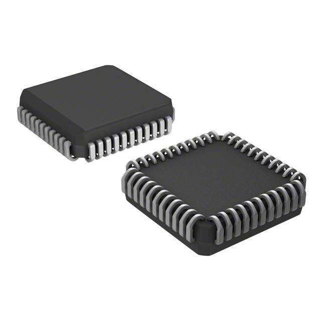
| 产品图片 |
|
| rohs | 符合RoHS无铅 / 符合限制有害物质指令(RoHS)规范要求 |
| 产品系列 | 音频 IC,音频数/模转换器 IC,Texas Instruments PCM1753DBQR- |
| 数据手册 | |
| 产品型号 | PCM1753DBQR |
| PCN组件/产地 | |
| 产品培训模块 | http://www.digikey.cn/PTM/IndividualPTM.page?site=cn&lang=zhs&ptm=13240 |
| 产品目录页面 | |
| 产品种类 | 音频数/模转换器 IC |
| 位数 | 24 |
| 供应商器件封装 | 16-SSOP |
| 信噪比 | 106 dB |
| 其它名称 | 296-26301-1 |
| 分辨率 | 24 bit |
| 制造商产品页 | http://www.ti.com/general/docs/suppproductinfo.tsp?distId=10&orderablePartNumber=PCM1753DBQR |
| 包装 | 剪切带 (CT) |
| 单位重量 | 70 mg |
| 商标 | Texas Instruments |
| 安装类型 | 表面贴装 |
| 安装风格 | SMD/SMT |
| 封装 | Reel |
| 封装/外壳 | 16-SSOP(0.154",3.90mm 宽) |
| 封装/箱体 | SSOP-16 |
| 工作温度 | -25°C ~ 85°C |
| 工作温度范围 | + 85 C |
| 工作电源电压 | 5 V |
| 工厂包装数量 | 2000 |
| 建立时间 | - |
| 接口类型 | Serial (3-Wire) |
| 数据接口 | 串行 |
| 标准包装 | 1 |
| 电压源 | 单电源 |
| 系列 | PCM1753 |
| 转换器数 | 2 |
| 转换器数量 | 2 |
| 转换速率 | 192 kHz |
| 输出数和类型 | 2 电压,单极 |
| 通道数量 | 2 Channel |
| 采样率(每秒) | 192k |


- 商务部:美国ITC正式对集成电路等产品启动337调查
- 曝三星4nm工艺存在良率问题 高通将骁龙8 Gen1或转产台积电
- 太阳诱电将投资9.5亿元在常州建新厂生产MLCC 预计2023年完工
- 英特尔发布欧洲新工厂建设计划 深化IDM 2.0 战略
- 台积电先进制程称霸业界 有大客户加持明年业绩稳了
- 达到5530亿美元!SIA预计今年全球半导体销售额将创下新高
- 英特尔拟将自动驾驶子公司Mobileye上市 估值或超500亿美元
- 三星加码芯片和SET,合并消费电子和移动部门,撤换高东真等 CEO
- 三星电子宣布重大人事变动 还合并消费电子和移动部门
- 海关总署:前11个月进口集成电路产品价值2.52万亿元 增长14.8%


PDF Datasheet 数据手册内容提取
Product Order Technical Tools & Support & Folder Now Documents Software Community PCM1753,PCM1754,PCM1755 SLES092E–APRIL2003–REVISEDJULY2019 PCM175x 24-Bit, 192-kHz Sampling, Enhanced Multilevel, Delta-Sigma, Audio, Digital-to-Analog Converter 1 Features 3 Description • 24-bitresolution The PCM1753, PCM1754, and PCM1755 (PCM175x) 1 devices are stereo digital-to-analog converters • Analogperformance(V =5V) CC (DACs) based on TI's enhanced delta-sigma – Dynamicrange:106dB architecture.This enhanced architecture employs 4th- – SNR:106dB,typical order noise shaping and 8-level amplitude quantization to achieve excellent dynamic – THD+N:0.002%,typical performance and improved clock jitter tolerance. The – Full-scaleoutput:4VPP,typical PCM175x devices easily interface with audio DSP • 4× or8×oversamplingdigitalfilter and decoder chips because of the devices support of industry-standard audio data formats with 16-bit and – Stop-bandattenuation: –50dB 24-bit data. The PCM175x devices can be controlled – Pass-bandripple:±0.04dB in a hardware mode, or through a full set of user- • Samplingfrequency:5kHzto200kHz programmablefunctionsthatareaccessible through a three-wire serial control port that supports register- • Systemclock:128f ,192f ,256f ,384f ,512 S S S S writefunctions. f ,768f ,1152f withautodetect S S S • Hardwarecontrol(PCM1754) The PCM1753 is pin compatible with the PCM1748, PCM1742,andPCM1741,exceptforpin5. – I2Sand16-bitword,right-justified – 44.1kHzdigitalde-emphasis DeviceInformation(1) – Softmute PARTNUMBER PACKAGE BODYSIZE(NOM) – ZeroflagforL-,R-channelcommonoutput PCM1753 • Powersupply:5-Vsinglesupply PCM1754 SSOP(16) 3.90mm×4.90mm • Small16-leadSSOPpackage,lead-free PCM1755 (1) Forallavailablepackages,seethepackageoptionaddendum 2 Applications attheendofthedatasheet. • A/Vreceivers • HDTVreceivers • Caraudiosystems • Applicationsrequiring24-bitaudio FunctionalBlockDiagram BCK LRCK Audio Output Amp VOUTL DATA SPeoriratl DAC And Low-Pass Filter 4x/8x Enhanced FMT Oversampling Multilevel Digital Filter Delta-Sigma VCOM and Function Modulator MUTE Serial Control Control Port Output Amp DEMP DAC And Low-Pass Filter VOUTR TEST System Clock SCK System Zero Detect Power Supply Clock Manager ZEROA DGND VCC AGND 1 An IMPORTANT NOTICE at the end of this data sheet addresses availability, warranty, changes, use in safety-critical applications, intellectualpropertymattersandotherimportantdisclaimers.PRODUCTIONDATA.
PCM1753,PCM1754,PCM1755 SLES092E–APRIL2003–REVISEDJULY2019 www.ti.com Table of Contents 1 Features.................................................................. 1 8.4 DeviceFunctionalModes........................................17 2 Applications........................................................... 1 8.5 Programming...........................................................18 3 Description............................................................. 1 8.6 RegisterMaps.........................................................19 4 RevisionHistory..................................................... 2 9 ApplicationandImplementation........................ 24 9.1 ApplicationInformation............................................24 5 DeviceComparisonTable..................................... 3 9.2 TypicalApplication .................................................24 6 PinConfigurationandFunctions......................... 3 10 PowerSupplyRecommendations..................... 29 7 Specifications......................................................... 4 11 Layout................................................................... 29 7.1 AbsoluteMaximumRatings......................................4 11.1 LayoutGuidelines.................................................29 7.2 ESDRatings..............................................................4 11.2 LayoutExample....................................................29 7.3 RecommendedOperatingConditions......................4 12 DeviceandDocumentationSupport................. 31 7.4 ThermalInformation..................................................4 7.5 ElectricalCharacteristics...........................................5 12.1 RelatedDocumentation .......................................31 7.6 SystemClockInputTiming.......................................6 12.2 RelatedLinks........................................................31 7.7 AudioInterfaceTiming..............................................6 12.3 ReceivingNotificationofDocumentationUpdates31 7.8 ControlInterfaceTimingRequirements....................7 12.4 CommunityResources..........................................31 7.9 TypicalCharacteristics..............................................8 12.5 Trademarks...........................................................31 12.6 ElectrostaticDischargeCaution............................31 8 DetailedDescription............................................ 12 12.7 Glossary................................................................31 8.1 Overview.................................................................12 13 Mechanical,Packaging,andOrderable 8.2 FunctionalBlockDiagram.......................................12 Information........................................................... 32 8.3 FeatureDescription.................................................12 4 Revision History NOTE:Pagenumbersforpreviousrevisionsmaydifferfrompagenumbersinthecurrentversion. ChangesfromRevisionD(August2015)toRevisionE Page • Addedtexttopin11descriptiontoclarifyoperationforPCM1755........................................................................................ 3 • Addedtexttopin12descriptiontoclarifyoperationforPCM1755 ....................................................................................... 3 • AddednewrowforPCM1755temperaturerangetoAbsoluteMaximumRatingstable ....................................................... 4 • ChangedlocationofoperatingtemperaturefromElectricalCharacteristicstabletoRecommendedOperating Conditionstable...................................................................................................................................................................... 4 • ChangedoperatingtemperatureMAXvalueforPCM1753andPCM1754from105°Cto85°CintheRecommended OperatingConditionstable..................................................................................................................................................... 4 • AddednewrowforPCM1755temperaturerangetotheRecommendedOperatingConditionstable ................................. 4 • ChangedoutputvoltagevaluefromMINtoTYPintheElectricalCharacteristicstable ....................................................... 6 • ChangedcentervoltagevaluefromMINtoTYPintheElectricalCharacteristicstable........................................................ 6 ChangesfromRevisionC(February2009)toRevisionD Page • AddedESDRatingstable,RecommendedOperatingConditionstable,FeatureDescriptionsection,Device FunctionalModes,ApplicationandImplementationsection,PowerSupplyRecommendationssection,Layout section,DeviceandDocumentationSupportsection,andMechanical,Packaging,andOrderableInformationsection......1 2 SubmitDocumentationFeedback Copyright©2003–2019,TexasInstrumentsIncorporated ProductFolderLinks:PCM1753 PCM1754 PCM1755
PCM1753,PCM1754,PCM1755 www.ti.com SLES092E–APRIL2003–REVISEDJULY2019 5 Device Comparison Table FEATURE PCM1753,PCM1755 PCM1754 Audiodatainterfaceformat I2S,standard,left-justified I2S,standard Audiodatabitlength 16-bit,18-bit,20-bit,and24-bitselectable 16-bitand24-bitI2S,16-bitstandard Audiodataformat MSBfirst,2'scomplement 6 Pin Configuration and Functions PCM1753,PCM1755DBQPackage PCM1754DBQPackage 16-PinSSOP 16-PinSSOP TopView TopView BCK 1 16 SCK BCK 1 16 SCK DATA 2 15 ML DATA 2 15 FMT LRCK 3 14 MC LRCK 3 14 MUTE DGND 4 13 MD DGND 4 13 DEMP NC 5 12 ZEROL/NA NC 5 12 TEST V 6 11 ZEROR/ZEROA V 6 11 ZEROA CC CC V L 7 10 V V L 7 10 V OUT COM OUT COM VOUTR 8 9 AGND VOUTR 8 9 AGND PinFunctions PIN PCM1753, I/O DESCRIPTION NAME PCM1754 PCM1755 AGND 9 9 — Analogground BCK 1 1 I Audio-databit-clockinput DATA 2 2 I Audio-datadigitalinput DEMP - 13 I De-emphasiscontrol DGND 4 4 — Digitalground FMT - 15 I Dataformatselect LRCK 3 3 I L-channelandR-channelaudiodatalatchenableinput MC 14 - I Modecontrolclockinput MD 13 - I Modecontroldatainput ML 15 - I Modecontrollatchinput MUTE - 14 I Analogmixingcontrol NC 5 5 — Noconnection SCK 16 16 I Systemclockinput TEST - 12 I Testpin,groundoropen VCC 6 6 — Analogpowersupply,5V VCOM 10 10 — Commonvoltagedecoupling VOUTL 7 7 O AnalogoutputforL-channel VOUTR 8 8 O AnalogoutputforR-channel ZeroflagoutputforR-channel/ZeroflagoutputforL-/R-channel. ZEROR/ZEROA 11 11 O Open-drainoutputforPCM1755. ZeroflagoutputforL-channel/Notassigned. ZEROL/NA 12 - O Open-drainoutputforPCM1755. Copyright©2003–2019,TexasInstrumentsIncorporated SubmitDocumentationFeedback 3 ProductFolderLinks:PCM1753 PCM1754 PCM1755
PCM1753,PCM1754,PCM1755 SLES092E–APRIL2003–REVISEDJULY2019 www.ti.com 7 Specifications 7.1 Absolute Maximum Ratings(1) overoperatingfree-airtemperaturerange(unlessotherwisenoted) MIN MAX UNIT Supplyvoltage V –0.3 6.5 V CC Groundvoltagedifferences AGND,DGND ±0.1 V Inputvoltage –0.3 6.5 V Inputcurrent(anypinsexceptsupplies) ±10 mA PCM1753,PCM1754 –40 85 Ambienttemperatureunderbias °C PCM1755 –25 85 Junctiontemperature 150 °C Storagetemperature,T –55 150 °C stg (1) StressesbeyondthoselistedunderAbsoluteMaximumRatingsmaycausepermanentdamagetothedevice.Thesearestressratings only,andfunctionaloperationofthedeviceattheseoranyotherconditionsbeyondthoseindicatedisnotimplied.Exposuretoabsolute- maximum-ratedconditionsforextendedperiodsmayaffectdevicereliability. 7.2 ESD Ratings VALUE UNIT Human-bodymodel(HBM),perANSI/ESDA/JEDECJS-001(1) ±2000 V Electrostaticdischarge V (ESD) Charged-devicemodel(CDM),perJEDECspecificationJESD22-C101(2) ±750 (1) JEDECdocumentJEP155statesthat500-VHBMallowssafemanufacturingwithastandardESDcontrolprocess. (2) JEDECdocumentJEP157statesthat250-VCDMallowssafemanufacturingwithastandardESDcontrolprocess. 7.3 Recommended Operating Conditions overoperatingfree-airtemperaturerange(unlessotherwisenoted) MIN NOM MAX UNIT V Supplyvoltage 4.5 5 5.5 V CC PCM1753,PCM1754 –40 85 T Operatingtemperature °C A PCM1755 –25 85 7.4 Thermal Information PCM175x THERMALMETRIC(1) DBQ(SSOP) UNIT 16PINS R Junction-to-ambientthermalresistance 104.1 °C/W θJA R Junction-to-case(top)thermalresistance 53 °C/W θJC(top) R Junction-to-boardthermalresistance 46.9 °C/W θJB ψ Junction-to-topcharacterizationparameter 10.3 °C/W JT ψ Junction-to-boardcharacterizationparameter 46.4 °C/W JB R Junction-to-case(bottom)thermalresistance N/A °C/W θJC(bot) (1) Formoreinformationabouttraditionalandnewthermalmetrics,seetheSemiconductorandICPackageThermalMetricsapplication report. 4 SubmitDocumentationFeedback Copyright©2003–2019,TexasInstrumentsIncorporated ProductFolderLinks:PCM1753 PCM1754 PCM1755
PCM1753,PCM1754,PCM1755 www.ti.com SLES092E–APRIL2003–REVISEDJULY2019 7.5 Electrical Characteristics allspecificationsatT =25°C,V =5V,f =44.1kHz,systemclock=384f ,and24-bitdata(unlessotherwisenoted) A CC S S PARAMETER TESTCONDITIONS MIN TYP MAX UNIT Resolution 24 Bits DATAFORMAT f Samplingfrequency 5 200 kHz S 128f S 192f S 256f S Systemclockfrequency 384f kHz S 512f S 768f S 1152f S DIGITALINPUT/OUTPUT Logicfamily TTLcompatible V Inputlogiclevel,high 2 VDC IH V Inputlogiclevel,low 0.8 VDC IL Inputlogiccurrent,high(SCK,BCK,DATA, I V =V 10 µA IH andLRCKpins) IN CC Inputlogiccurrent,low(SCK,BCK,DATA, I V =0V -10 µA IL andLRCKpins) IN Inputlogiccurrent,high(TEST,DEMP, I V =V 65 100 µA IH MUTE,andFMTpins) IN CC Inputlogiccurrent,low(TEST,DEMP, I V =0V -10 µA IL MUTE,andFMTpins) IN V Outputlogiclevel,high(ZEROApin) I =–1mA 2.4 VDC OH OH V Outputlogiclevel,low(ZEROApin) I =1mA 0.4 VDC OL OL DYNAMICPERFORMANCE(1)(2) f =44.1kHz 0% 0.01% S THD+NatVOUT=0dB f =96kHz 0% S f =192kHz 0% S f =44.1kHz 0.65% S THD+NatVOUT=-60dB f =96kHz 0.80% S f =192kHz 0.95% S EIAJ,A-weighted,f =44.1kHz 100 106 S Dynamicrange A-weighted,f =96kHz 104 dB S A-weighted,f =192kHz 102 S EIAJ,A-weighted,f =44.1kHz 100 106 S Signal-to-noiseratio A-weighted,f =96kHz 104 dB S A-weighted,f =192kHz 102 S f =44.1kHz 97 103 S Channelseparation f =96kHz 101 dB S f =192kHz 100 S Levellinearityerror VOUT=-90dB ±0.5 dB DCACCURACY %of Gainerror ±1 ±6 FSR %of Gainmismatch,channel-to-channel ±1 ±3 FSR Bipolarzeroerror VOUT=0.5V atBPZ ±30 ±60 mV CC (1) AnalogperformancespecificationsaremeasuredusingtheSystemTwo™CascadeaudiomeasurementsystembyAudioPrecision™in theaveragingmode. (2) Conditionsin192-kHzoperationaresystemclock=128f andoversamplingrate=64f ofregister18. S S Copyright©2003–2019,TexasInstrumentsIncorporated SubmitDocumentationFeedback 5 ProductFolderLinks:PCM1753 PCM1754 PCM1755
PCM1753,PCM1754,PCM1755 SLES092E–APRIL2003–REVISEDJULY2019 www.ti.com Electrical Characteristics (continued) allspecificationsatT =25°C,V =5V,f =44.1kHz,systemclock=384f ,and24-bitdata(unlessotherwisenoted) A CC S S PARAMETER TESTCONDITIONS MIN TYP MAX UNIT ANALOGOUTPUT 80%of Outputvoltage Fullscale(0dB) V V PP CC 50%of Centervoltage VDC V CC Loadimpedance AC-coupledload 5 kΩ DIGITALFILTERPERFORMANCE FILTERCHARACTERISTICS(SHARPROLLOFF) Passband ±0.04dB 0.454f S Stopband 0.546fs Pass-bandripple ±0.04 dB Stop-bandattenuation Stopband=0.546f –50 dB S ANALOGFILTERPERFORMANCE At20kHz –0.03 Frequencyresponse dB At44kHz –0.2 POWERSUPPLYREQUIREMENTS(2) f =44.1kHz 16 21 S I Supplycurrent f =96kHz 25 mA CC S f =192kHz 30 S f =44.1kHz 80 105 S Powerdissipation f =96kHz 125 mW S f =192kHz 150 S TEMPERATURE R ThermalResistance 16-pinDBQ 104.1 °C/W θJA 7.6 System Clock Input Timing formoreinformation,seetheSystemClockInputsection MIN NOM MAX UNIT t Systemclockpulseduration,high 7 ns (SCKH) t Systemclockpulseduration,low SeeFigure20. 7 ns (SCKL) t Systemclockpulsecycletime See (1) ns (SCY) (1) 1/128f ,1/256f ,1/384f ,1/512f ,1/768f ,or1/1152f . S S S S S S 7.7 Audio Interface Timing formoreinformation,seetheAudioDataFormatsandTimingsection MIN MAX UNIT 1/(32f ) S t BCKpulsecycletime 1/(48f ) (BCY) S 1/(64f )(1) S t BCKhigh–leveltime 35 ns (BCH) t BCKlow–leveltime 35 ns (BCL) SeeFigure22. t BCKrisingedgetoLRCKedge 10 ns (BL) LRCKfallingedgetoBCKrising t 10 ns (LB) edge t DATAsetuptime 10 ns (DS) t DATAholdtime 10 ns (DH) (1) f isthesamplingfrequency(forexample,44.1kHz,48kHz,96kHz,andsoon). S 6 SubmitDocumentationFeedback Copyright©2003–2019,TexasInstrumentsIncorporated ProductFolderLinks:PCM1753 PCM1754 PCM1755
PCM1753,PCM1754,PCM1755 www.ti.com SLES092E–APRIL2003–REVISEDJULY2019 7.8 Control Interface Timing Requirements thesetimingparametersarecriticalforpropercontrolportoperation MIN NOM MAX UNIT t MCpulsecycletime 100 ns (MCY) t MClow-leveltime 50 ns (MCL) t MChigh-leveltime 50 ns (MCH) t MLhigh-leveltime See (1) ns (MCH) SeeFigure1. t MLfallingedgetoMCrisingedge 20 ns (MLS) t MLholdtime(2) 20 ns (MLH) t MDholdtime 15 ns (MDH) t MDsetuptime 20 ns (MCS) 3 256´ f (1) S seconds(min);f :samplingrate. S (2) MCrisingedgeforLSBtoMLrisingedge. t (MHH) ML t t (MLS) (MCL) t(MCH) t(MLH) MC t (MCY) LSB MD t (MDS) t (MDH) Figure1. ControlInterfaceTiming Copyright©2003–2019,TexasInstrumentsIncorporated SubmitDocumentationFeedback 7 ProductFolderLinks:PCM1753 PCM1754 PCM1755
PCM1753,PCM1754,PCM1755 SLES092E–APRIL2003–REVISEDJULY2019 www.ti.com 7.9 Typical Characteristics 7.9.1 DigitalFilter(De-EmphasisOff) allspecificationsatT =25°C,V =5V,f =44.1kHz,systemclock=384f ,and24-bitdata,(unlessotherwisenoted) A CC S S 0 0.05 0.04 –20 0.03 –40 0.02 dB) –60 dB) 0.01 de ( de ( 0.00 u u mplit –80 mplit –0.01 A A –100 –0.02 –0.03 –120 –0.04 –140 –0.05 0 1 2 3 4 0.0 0.1 0.2 0.3 0.4 0.5 Frequency[×fS] Frequency[×fS] Figure2.FrequencyResponse,SharpRolloff Figure3.Pass-BandRipple,SharpRolloff 0 5 4 –20 3 –40 2 dB) –60 dB) 1 de ( de ( 0 u u mplit –80 mplit –1 A A –100 –2 –3 –120 –4 –140 –5 0 1 2 3 4 0.0 0.1 0.2 0.3 0.4 0.5 Frequency[×fS] Frequency [×fS] Figure4.FrequencyResponse,SlowRolloff Figure5.TransitionCharacteristics,SlowRolloff 0 0.5 –1 0.4 –2 0.3 B) –3 B) 0.2 asis Level (d ––45 asis Error (d 00..01 ph –6 ph –0.1 m m e e e- –7 e- –0.2 D D –8 –0.3 –9 –0.4 –10 –0.5 0 2 4 6 8 10 12 14 0 2 4 6 8 10 12 14 Frequency (kHz) Frequency (kHz) Figure6.De-EmphasisLevelvsFrequency Figure7.De-EmphasisErrorvsFrequency 8 SubmitDocumentationFeedback Copyright©2003–2019,TexasInstrumentsIncorporated ProductFolderLinks:PCM1753 PCM1754 PCM1755
PCM1753,PCM1754,PCM1755 www.ti.com SLES092E–APRIL2003–REVISEDJULY2019 Digital Filter (De-Emphasis Off) (continued) allspecificationsatT =25°C,V =5V,f =44.1kHz,systemclock=384f ,and24-bitdata,(unlessotherwisenoted) A CC S S 0 0.5 –1 0.4 –2 0.3 asis Level (dB) –––435 asis Error (dB) 000...021 ph –6 ph –0.1 m m e e e- –7 e- –0.2 D D –8 –0.3 –9 –0.4 –10 –0.5 0 2 4 6 8 10 12 14 16 18 20 0 2 4 6 8 10 12 14 16 18 20 Frequency (kHz) Frequency (kHz) Figure8.De-EmphasisLevelvsFrequency Figure9.De-EmphasisErrorvsFrequency 0 0.5 –1 0.4 –2 0.3 B) –3 B) 0.2 asis Level (d ––45 asis Error (d 00..01 ph –6 ph –0.1 m m e e e- –7 e- –0.2 D D –8 –0.3 –9 –0.4 –10 –0.5 0 2 4 6 8 10 12 14 16 18 20 22 0 2 4 6 8 10 12 14 16 18 20 22 Frequency (kHz) Frequency (kHz) Figure10.De-EmphasisLevelvsFrequency Figure11.De-EmphasisErrorvsFrequency Copyright©2003–2019,TexasInstrumentsIncorporated SubmitDocumentationFeedback 9 ProductFolderLinks:PCM1753 PCM1754 PCM1755
PCM1753,PCM1754,PCM1755 SLES092E–APRIL2003–REVISEDJULY2019 www.ti.com 7.9.2 AnalogDynamicPerformance(SupplyVoltageCharacteristics) AllspecificationsatT =25°C,V =5V,f =44.1kHz,systemclock=384f ,and24-bitdata,(unlessotherwisenoted) A CC S S 10 110 44.1 kHz, 384 fS 96 kHz, 384 fS se (%) 1 –60 dB 110068 192 kHz, 128 fS oi armonic Distortion + N 00.0.11 0 dB Dynamic Range (dB) 111000024 H al 0.001 Tot 44.1 kHz, 384 fS 98 96 kHz, 384 fS 192 kHz, 128 fS 0.0001 96 4.0 4.5 5.0 5.5 6.0 4.0 4.5 5.0 5.5 6.0 Supply Voltage (V) Supply Voltage (V) Figure12.TotalHarmonicDistortion+NoisevsSupply Figure13.DynamicRangevsSupplyVoltage Voltage 110 110 44.1 kHz, 384 fS 44.1 kHz, 384 fS 96 kHz, 384 fS 96 kHz, 384 fS 108 192 kHz, 128 fS 108 192 kHz, 128 fS Ratio (dB) 110046 ation (dB) 110046 e ar Nois 102 Sep 102 o- el Signal-t 100 Chann 100 98 98 96 96 4.0 4.5 5.0 5.5 6.0 4.0 4.5 5.0 5.5 6.0 Supply Voltage (V) Supply Voltage (V) Figure14.Signal-to-NoiseRatiovsSupplyVoltage Figure15.ChannelSeparationvsSupplyVoltage 10 SubmitDocumentationFeedback Copyright©2003–2019,TexasInstrumentsIncorporated ProductFolderLinks:PCM1753 PCM1754 PCM1755
PCM1753,PCM1754,PCM1755 www.ti.com SLES092E–APRIL2003–REVISEDJULY2019 7.9.3 AnalogDynamicPerformance(TemperatureCharacteristics) AllspecificationsatT =25°C,V =5V,f =44.1kHz,systemclock=384f ,and24-bitdata,(unlessotherwisenoted) A CC S S 10 110 44.1 kHz, 384 fS 96 kHz, 384 fS %) 1 –60 dB 108 192 kHz, 128 fS e ( ois 106 on + N 0.1 e (dB) 104 armonic Distorti 0.01 0dB Dynamic Rang 110002 H Total 0.001 44.1 kHz, 384 fS 98 96 kHz, 384 fS 192 kHz, 128 fS 0.0001 96 –50 –25 0 25 50 75 100 –50 –25 0 25 50 75 100 Free-AirTemperature(°C) Free-AirTemperature(°C) Figure16.TotalHarmonicDistortion+NoisevsFree-Air Figure17.DynamicRangevsFree-AirTemperature Temperature 110 110 44.1 kHz, 384 fS 44.1 kHz, 384 fS 96 kHz, 384 fS 96 kHz, 384 fS 108 192 kHz, 128 fS 108 192 kHz, 128 fS 106 106 B) Ratio (dB) 104 paration (d 104 Noise 102 nel Se 102 al-to- 100 Chan 100 n g Si 98 98 96 96 –50 –25 0 25 50 75 100 –50 –25 0 25 50 75 100 Free-AirTemperature(°C) Free-AirTemperature(°C) Figure18.Signal-to-NoiseRatiovsFree-AirTemperature Figure19.ChannelSeparationvsFree-AirTemperature Copyright©2003–2019,TexasInstrumentsIncorporated SubmitDocumentationFeedback 11 ProductFolderLinks:PCM1753 PCM1754 PCM1755
PCM1753,PCM1754,PCM1755 SLES092E–APRIL2003–REVISEDJULY2019 www.ti.com 8 Detailed Description 8.1 Overview The PCM175x devices are stereo digital-to-analog converters (DACs) based on TI's enhanced delta-sigma architecture which employ 4th-order noise shaping and 8-level amplitude quantization to achieve excellent dynamic performance and improved clock jitter tolerance. The PCM175x devices easily interface with audio DSP and decoder chips because of the devices' support of industry-standard audio data formats with 16- and 24-bit data. The PCM175x devices can be controlled in a hardware mode, or a full set of user-programmable functions isaccessiblethroughathree-wireserialcontrolport,whichsupportsregister-writefunctions. 8.2 Functional Block Diagram BCK Audio LRCK Serial OutputAmp VOUTL DATA Port DAC and Low-Pass Filter 4x/8x Oversampling Enhanced Digital Multilevel FMT Filter Delta-Sigma VCOM and Modulator Function MUTE Serial Control Control Port OutputAmp DAC and DEMP Low-Pass Filter VOUTR TEST System Clock System SCK Clock ZeroDetect Power Supply Manager A D C D RO GN VC GN E D A Z 8.3 Feature Description 8.3.1 SystemClockandResetFunctions 8.3.1.1 SystemClockInput The PCM175x devices require a system clock for operating the digital interpolation filters and multilevel delta- sigma modulators. The system clock is applied at the SCK input (pin 16). Table 1 lists examples of system clock frequenciesforcommonaudiosamplingrates. Figure20showsand the System Clock Input Timing table lists he timing requirements for the system clock input. For optimal performance, use a clock source with low phase-jitter and noise. TI's PLL170x family of multiclock generatorsisanexcellentchoiceforprovidingthePCM175xsystemclock. 12 SubmitDocumentationFeedback Copyright©2003–2019,TexasInstrumentsIncorporated ProductFolderLinks:PCM1753 PCM1754 PCM1755
PCM1753,PCM1754,PCM1755 www.ti.com SLES092E–APRIL2003–REVISEDJULY2019 Feature Description (continued) Table1.SystemClockRatesforCommonAudioSamplingFrequencies SAMPLING SYSTEMCLOCKFREQUENCY(fSCLK)(MHz) FREQUENCY 128f 192f 256f 384f 512f 768f 1152f S S S S S S S 8kHz 1.024 1.536 2.048 3.072 4.096 6.144 9.216 16kHz 2.048 3.072 4.096 6.144 8.192 12.288 18.432 32kHz 4.096 6.144 8.192 12.288 16.384 24.576 36.864 44.1kHz 5.6448 8.4672 11.2896 16.9344 22.5792 33.8688 (1) 48kHz 6.144 9.216 12.288 18.432 24.576 36.864 (1) 88.2kHz 11.2896 16.9344 22.5792 33.8688 45.1584 (1) (1) 96kHz 12.288 18.432 24.576 36.864 49.152 (1) (1) 192kHz 24.576 36.864 (1) (1) (1) (1) (1) (1) Thissystemclockrateisnotsupportedforthegivensamplingfrequency. t(SCKH) H 2.0 V System Clock (SCK) 0.8 V L t(SCKL) t(SCY) Figure20. SystemClockInputTiming 8.3.1.2 Power-OnResetFunctions ThePCM175xdevicesincludeapower-onresetfunction.Figure21showstheoperationofthisfunction.Withthe system clock active and V > 3 V (typical, 2.2 V to 3.7 V), the power-on reset function is enabled. The CC initializationsequencerequires1024systemclocksfromthetimeV >3V(typical,2.2Vto3.7V). CC During the reset period (1024 system clocks), the analog output is forced to the bipolar zero level, or V /2. After CC the reset period, an internal register is initialized in the next 1/f period and if SCK, BCK, and LRCK are provided S continuously,thePCM175xdevicesprovideproperanalogoutputwithunitgroupdelayagainsttheinputdata. VCC 3.7 V (Max) 3.0 V (Typ) 2.2 V (Min) Reset ResetRemoval Internal Reset Don’t Care 1024 System Clocks System Clock Figure21. Power-OnResetTiming Copyright©2003–2019,TexasInstrumentsIncorporated SubmitDocumentationFeedback 13 ProductFolderLinks:PCM1753 PCM1754 PCM1755
PCM1753,PCM1754,PCM1755 SLES092E–APRIL2003–REVISEDJULY2019 www.ti.com 8.3.2 AudioSerialInterface The audio serial interface for the PCM175x devices consists of a 3-wire synchronous serial port. The interface includes LRCK (pin 3), BCK (pin 1), and DATA (pin 2). The BCK pin is the serial audio bit clock, and it is used to clock the serial data present on the DATA pin into the serial shift register of the audio interface. Serial data is clocked into the PCM175x on the rising edge of the BCK pin. The LRCK pin is the serial audio left and right word clock.Thispinisusedtolatchserialdataintotheinternalregistersoftheserialaudiointerface. Both the LRCK and BCK pins should be synchronous to the system clock. Ideally, TI recommendeds that the LRCK and BCK pins be derived from the system clock input, SCK. The LRCK pin is operated at the sampling frequency, f . The BCK pin can be operated at 32, 48, or 64 times the sampling frequency for standard (right- S justified)format,and32timesthesamplingfrequencyoftheBCKpinislimitedto 16-bit right-justified format only. The BCK pin can be operated at 48 or 64 times the sampling frequency for the I2S and left-justified formats. 48 timesthesamplingfrequencyofBCKislimitedto192/384/768f SCKI. S Internal operation of the PCM175x devices is synchronized with the LRCK pin. Accordingly, internal operation is held when the sampling rate clock of the LRCK pin is changed or when the SCK pin and/or BCK pin is interrupted for a 3-bit clock cycle or longer. If th SCK, BCK, and LRCK pins are provided continuously after this held condition, the internal operation is re-synchronized automatically in a period of less than 3/f . External S resettingisnotrequired. 8.3.2.1 AudioDataFormatsandTiming The PCM1753 device supports industry-standard audio data formats, including right-justified, I2S, and left- justified. The PCM1754 device supports I2S and 16-bit-word right-justified audio data formats. Figure 23 shows the data formats. Data formats are selected using the format bits, FMT[2:0], located in control register 20 of the PCM1753 device, and are selected using the FMT pin on the PCM1754 device. The default data format is 24-bit left-justified. All formats require binary 2s-complement MSB-first audio data. The Audio Interface Timing table showsadetailedtimingdiagramfortheserialaudiointerface. LRCK 1.4V t(BCH) t(BCL) t(LB) BCK 1.4 V t(BCY) t(BL) DATA 1.4 V t(DS) t(DH) Figure22. AudioInterfaceTiming 14 SubmitDocumentationFeedback Copyright©2003–2019,TexasInstrumentsIncorporated ProductFolderLinks:PCM1753 PCM1754 PCM1755
PCM1753,PCM1754,PCM1755 www.ti.com SLES092E–APRIL2003–REVISEDJULY2019 (1)StandardDataFormat;L-Channel=HIGH,R-Channel=LOW 1/fS LRCK L-Channel R-Channel BCK (=32fS,48fS,or64fS) 16-BitRight-Justified,BCK=48fSor64fS DATA 14 15 16 1 2 3 14 15 16 1 2 3 14 15 16 MSB LSB MSB LSB 16-BitRight-Justified,BCK=32fS DATA 14 15 16 1 2 3 14 15 16 1 2 3 14 15 16 MSB LSB MSB LSB 18-BitRight-Justified,BCK=48fSor64fS DATA 16 17 18 1 2 3 16 17 18 1 2 3 16 17 18 MSB LSB MSB LSB 20-BitRight-Justified,BCK=48fSor64fS DATA 18 19 20 1 2 3 18 19 20 1 2 3 18 19 20 MSB LSB MSB LSB 24-BitRight-Justified,BCK=48fSor64fS DATA 22 23 24 1 2 3 22 23 24 1 2 3 22 23 24 MSB LSB MSB LSB (2)I2S Data Format; L-Channel = LOW, R-Channel = HIGH 1/fS LRCK L-Channel R-Channel BCK (=48fSor64fS) DATA 1 2 3 N–2 N–1 N 1 2 3 N–2 N–1 N 12 MSB LSB MSB LSB (3) Left-Justified Data Format; L-Channel = HIGH, R-Channel = LOW 1/fS LRCK L-Channel R-Channel BCK (=48fS,or64fS) DATA 1 2 3 N–2 N–1 N 1 2 3 N–2 N–1 N 1 2 MSB LSB MSB LSB Figure23. AudioDataInputFormats Copyright©2003–2019,TexasInstrumentsIncorporated SubmitDocumentationFeedback 15 ProductFolderLinks:PCM1753 PCM1754 PCM1755
PCM1753,PCM1754,PCM1755 SLES092E–APRIL2003–REVISEDJULY2019 www.ti.com 8.3.3 ZeroFlag(PCM1754) The PCM1754 device has a ZERO flag pin, ZEROA (pin 11). ZEROA is the L-channel and R-channel common zero flag pin. If the data for L-channel and R-channel remains at a 0 level for 1024 sampling periods (or LRCK clockperiods),ZEROAissettoalogic1state. 8.3.4 ZeroFlag(PCM1753) Zero-DetectCondition Zero detection for either output channel is independent from the other channel. If the data for a given channel remains at a 0 level for 1024 sample periods (or LRCK clock periods), a zero-detect condition exists for that channel. 8.3.5 ZeroFlagOutputs If a zero-detect condition exists for one or more channels, the zero flag pins for those channels are set to a logic 1state.Therearezeroflagpinsforeachchannel,ZEROL(pin12)andZEROR(pin11).Thesepinscan be used to operate external mute circuits, or used as status indicators for a microcontroller, audio signal processor, or other digitally controlled function. The active polarity of zero flag outputs can be inverted by setting the ZREV bit of control register 22 to 1. The reset default is active-high output, or ZREV = 0. The L-channel and R-channel common zero flag can be selected by setting the AZRO bit of control register 22 to 1. The reset default is independentzeroflagsforL-channelandR-channel,orAZRO=0. 8.3.6 AnalogOutputs The PCM1753 device includes two independent output channels, V L and V R. These are unbalanced OUT OUT outputs, each capable of driving 4 V typical into a 5-kΩ ac-coupled load. The internal output amplifiers for PP V LandV Rarebiasedtothedccommon-mode(orbipolarzero)voltage,equalto0.5V . OUT OUT CC The output amplifiers include an RC continuous-time filter, which helps to reduce the out-of-band noise energy presentattheDACoutputsduetothenoiseshapingcharacteristicsofthePCM1754delta-sigma D/A converters. The frequency response of this filter is shown in Figure 24. By itself, this filter is not enough to attenuate the out- of-band noise to an acceptable level for many applications. An external low-pass filter is required to provide sufficient out-of-band noise rejection. Further discussion of DAC post-filter circuits is provided in the Applications Informationsectionofthisdatasheet. 10 0 –10 B) –20 d el ( ev –30 L –40 –50 –60 0.1 1 10 100 1k 10k Frequency (kHz) Figure24. OutputFilterFrequencyResponse 16 SubmitDocumentationFeedback Copyright©2003–2019,TexasInstrumentsIncorporated ProductFolderLinks:PCM1753 PCM1754 PCM1755
PCM1753,PCM1754,PCM1755 www.ti.com SLES092E–APRIL2003–REVISEDJULY2019 8.3.6.1 V Output COM Oneunbufferedcommon-modevoltageoutputpin, V (pin 10) is brought out for decoupling purposes. This pin COM is nominally biased to a dc voltage level equal to 0.5 V . This pin can be used to bias external circuits. CC Figure25showsanexampleofusingtheV pinforexternalbiasingapplications. COM R A =–1, where A =– 2 V V R 1 PCM1754 R2 C1 VCC R1 R3 2 10µF VOUTX(1) – 1/2 1 + Filtered OPA2353 C2 3 + Output VCOM + 10µF (1)X = L or R (a) Using VCOMto Bias a Single-Supply Filter Stage VCC PCM1754 – OPA337 Buffered VCOM VCOM + + 10µF (b)UsingaVoltageFollowertoBufferVCOMWhen Biasing Multiple Nodes Figure25. BiasingExternalCircuitsUsingtheV Pin COM 8.4 Device Functional Modes 8.4.1 HardwareControl(PCM1754) The digital functions of the PCM1754 are capable of hardware control. Table 2 lists selectable formats, Table 3 showsde-emphasiscontrol,andTable4listsmutecontrol. Table2.DataFormatSelect FMT(PIN15) DATAFORMAT LOW 16–to24–bit,I2Sformat HIGH 16–bitright–justified Copyright©2003–2019,TexasInstrumentsIncorporated SubmitDocumentationFeedback 17 ProductFolderLinks:PCM1753 PCM1754 PCM1755
PCM1753,PCM1754,PCM1755 SLES092E–APRIL2003–REVISEDJULY2019 www.ti.com Table3.De-EmphasisControl DEMP(PIN13) DE–EMPHASISFUNCTION LOW 44.1kHzde–emphasisOFF HIGH 44.1kHzde–emphasisON Table4.MuteControl MUTE(PIN14) MUTE LOW MuteOFF HIGH MuteON 8.4.2 OversamplingRateControl(PCM1754) The PCM1754 automatically controls the oversampling rate of the delta-sigma DACs with the system clock rate. Theoversamplingrateissetto64×oversamplingwitheverysystemclockandsamplingfrequency. 8.5 Programming 8.5.1 SoftwareControl(PCM1753/55) The PCM1753 and PCM1755 devices have many programmable functions which can be controlled in the softwarecontrolmode.The functions are controlled by programming the internal registers using the ML, MC, and MDpins. The serial control interface is a 3-wire serial port, which operates asynchronously to the audio serial interface. The serial control interface is used to program the on-chip mode registers. The control interface includes MD (pin 13), MC (pin 14), and ML (pin 15). The MD pin is the serial data input, used to program the mode registers. The MCpinistheserialbitclock,usedtoshiftdataintothecontrolport.TheMLpinisthecontrolportlatchclock. 8.5.1.1 RegisterWriteOperation All write operations for the serial control port use 16-bit data words. Figure 26 lists the control data word format. The most significant bit must be a 0. There are seven bits, labeled IDX[6:0], that set the register index (or address) for the write operation. The least significant eight bits, D[7:0], contain the data to be written to the registerspecifiedbyIDX[6:0]. Figure 27 lists the functional timing diagram for writing to the serial control port. ML is held at a logic 1 state until a register needs to be written. To start the register write cycle, ML is set to logic 0. Sixteen clocks are then provided on MC, corresponding to the 16 bits of the control data word on MD. After the sixteenth clock cycle has completed,MLissettologic1tolatchthedataintotheindexedmodecontrolregister. Figure26. ControlDataWordFormatforMD Figure27. RegisterWriteOperation 18 SubmitDocumentationFeedback Copyright©2003–2019,TexasInstrumentsIncorporated ProductFolderLinks:PCM1753 PCM1754 PCM1755
PCM1753,PCM1754,PCM1755 www.ti.com SLES092E–APRIL2003–REVISEDJULY2019 8.6 Register Maps 8.6.1 ModeControlRegisters(PCM1753/55) 8.6.1.1 User-ProgrammableModeControls The PCM1753/55 devices include a number of user-programmable functions, which are accessed via control registers. The registers are programmed using the serial control interface, which was previously discussed in this data sheet. Table 5 lists the available mode control functions, along with their reset default conditions and associatedregisterindex. Table5.User-ProgrammableModeControls FUNCTION RESETDEFAULT REGISTER BIT(s) Digitalattenuationcontrol,0dBto–63dBin0.5-dBsteps 0dB,noattenuation 16and17 AT1[7:0],AT2[7:0] Softmutecontrol Mutedisabled 18 MUT[2:0] Oversamplingratecontrol(64f or128f ) 64f oversampling 18 OVER S S S Softresetcontrol Resetdisabled 18 SRST DACoperationcontrol DAC1andDAC2enabled 19 DAC[2:1] De-emphasisfunctioncontrol De-emphasisdisabled 19 DM12 De-emphasissamplerateselection 44.1kHz 19 DMF[1:0] Audiodataformatcontrol 24-bitleft-justified 20 FMT[2:0] Digitalfilterrolloffcontrol Sharprolloff 20 FLT Zeroflagfunctionselect L-,R-channelindependent 22 AZRO Outputphaseselect Normalphase 22 DREV Zeroflagpolarityselect High 22 ZREV Themodecontrolregistermapisshownin Table 6. Each register includes an index (or address) indicated by the IDX[6:0]bits. Table6.ModeControlRegisterMap(1) IDX (B8–B REGISTER B15 B14 B13 B12 B11 B10 B9 B8 B7 B6 B5 B4 B3 B2 B1 B0 14) 10h Register16 0 IDX6 IDX5 IDX4 IDX3 IDX2 IDX1 IDX0 AT17 AT16 AT15 AT14 AT13 AT12 AT11 AT10 11h Register17 0 IDX6 IDX5 IDX4 IDX3 IDX2 IDX1 IDX0 AT27 AT26 AT25 AT24 AT23 AT22 AT21 AT20 12h Register18 0 IDX6 IDX5 IDX4 IDX3 IDX2 IDX1 IDX0 SRST OVER RSV RSV RSV RSV MUT2 MUT1 13h Register19 0 IDX6 IDX5 IDX4 IDX3 IDX2 IDX1 IDX0 RSV DMF1 DMF0 DM12 RSV RSV DAC2 DAC1 14h Register20 0 IDX6 IDX5 IDX4 IDX3 IDX2 IDX1 IDX0 RSV RSV FLT RSV RSV FMT2 FMT1 FMT0 16h Register22 0 IDX6 IDX5 IDX4 IDX3 IDX2 IDX1 IDX0 RSV RSV RSV RSV RSV AZRO ZREV DREV (1) RSV:Reservedfortestoperation.Itshouldbesetto0forregularoperation. Copyright©2003–2019,TexasInstrumentsIncorporated SubmitDocumentationFeedback 19 ProductFolderLinks:PCM1753 PCM1754 PCM1755
PCM1753,PCM1754,PCM1755 SLES092E–APRIL2003–REVISEDJULY2019 www.ti.com 8.6.1.2 RegisterDefinitions 8.6.1.2.1 ATx[7:0]:DigitalAttenuationLevelSetting Wherex=1or2,correspondingtotheDACoutputV L(x=1)andV R(x=2). OUT OUT Defaultvalue:11111111b Each DAC channel (V L and V R) includes a digital attenuation function. The attenuation level can be set OUT OUT from 0 dB to –63 dB in 0.5-dB steps. Changes in attenuator levels are made by incrementing or decrementing one step (0.5 dB) for every 8/fS time internal until the programmed attenuator setting is reached. Alternatively, theattenuationlevelcanbesettoinfiniteattenuation(ormute). The attenuation data for each channel can be set individually. The attenuation level is set using the following formula: Attenuationlevel(dB)=0.5× (ATx[7:0] –255) DEC whereATx[7:0] =0through255. DEC ForATx[7:0]DEC=0through128,attenuationissettoinfiniteattenuation. ThetableinFigure28showstheattenuationlevelsforvarioussettings: . . . . . . . . . . . . . . . . . . Figure28. ATx[7:0]:DigitalAttenuationLevelSettingTable 20 SubmitDocumentationFeedback Copyright©2003–2019,TexasInstrumentsIncorporated ProductFolderLinks:PCM1753 PCM1754 PCM1755
PCM1753,PCM1754,PCM1755 www.ti.com SLES092E–APRIL2003–REVISEDJULY2019 8.6.1.2.2 MUTx:SoftMuteControl wherex=1or2,correspondingtotheDACoutputsV L(x=1)andV R(x=2). OUT OUT Defaultvalue:0 The mute bits, MUT1 and MUT2, are used to enable or disable the soft mute function for the corresponding DAC outputs, VOUTL and VOUTR. The soft mute function is incorporated into the digital attenuators. When mute is disabled (MUTx = 0), the attenuator and DAC operate normally. When mute is enabled by setting MUTx = 1, the digital attenuator for the corresponding output is decreased from the current setting to infinite attenuation, one attenuatorstep(0.5dB)forevery8/fSseconds.Thisprovidespop-freemutingoftheDACoutput. By setting MUTx = 0, the attenuator is increased one step for every 8/fS seconds to the previously programmed attenuationlevel. 8.6.1.2.3 OVER:OversamplingRateControl Defaultvalue:0 Systemclockrate=256f ,384f ,512f ,768f ,or1152f : S S S S S Systemclockrate=128f or192f : S S The OVER bit is used to control the oversampling rate of the delta-sigma D/A converters. The OVER = 1 setting isrecommendedwhenthesamplingrateis192kHz(systemclockrateis128f or192f ). S S 8.6.1.2.4 SRST:Reset Defaultvalue:0 The SRST bit is used to enable or disable the soft reset function. The operation is the same as power-on reset. Allregistersareinitialized. 8.6.1.2.5 DACx:DACOperationControl Wherex=1or2,correspondingtotheDACoutputV L(x=1)orV R(x=2). OUT OUT Defaultvalue:0 The DAC operation controls are used to enable and disable the DAC outputs, V L and V R. When DACx = OUT OUT 0, the corresponding output generates the audio waveform dictated by the data present on the DATA pin. When DACx=1,thecorrespondingoutputissettothebipolarzerolevel,or0.5V . CC Copyright©2003–2019,TexasInstrumentsIncorporated SubmitDocumentationFeedback 21 ProductFolderLinks:PCM1753 PCM1754 PCM1755
PCM1753,PCM1754,PCM1755 SLES092E–APRIL2003–REVISEDJULY2019 www.ti.com 8.6.1.2.6 DM12:DigitalDe-EmphasisFunctionControl Defaultvalue:0 The DM12 bit is used to enable or disable the digital de-emphasis function. See the plots shown in the Typical Characteristicssectionofthisdatasheet. 8.6.1.2.7 DMF[1:0]:SamplingFrequencySelectionfortheDe-EmphasisFunction Defaultvalue:00 The DMF[1:0] bits are used to select the sampling frequency used for the digital de-emphasis function when it is enabled. 8.6.1.2.8 FMT[2:0]:AudioInterfaceDataFormat Defaultvalue:101 The FMT[2:0] bits are used to select the data format for the serial audio interface. The table in Figure 29 shows theavailableformatoptions. Figure29. FMT[2:0]:AudioInterfaceDataFormatTable 22 SubmitDocumentationFeedback Copyright©2003–2019,TexasInstrumentsIncorporated ProductFolderLinks:PCM1753 PCM1754 PCM1755
PCM1753,PCM1754,PCM1755 www.ti.com SLES092E–APRIL2003–REVISEDJULY2019 8.6.1.2.9 FLT:DigitalFilterRolloffControl Defaultvalue:0 The FLT bit allows the user to select the digital filter rolloff that is best suited to the application. Two filter rolloff selections are available, sharp and slow. The filter responses for these selections are shown in the Typical Characteristicssectionofthisdatasheet. 8.6.1.2.10 DREV:OutputPhaseSelect Defaultvalue:0 TheDREVbitistheoutputanalogsignalphasecontrol. 8.6.1.2.11 ZREV:ZeroFlagPolaritySelect Defaultvalue:01h TheZREVbitallowstheusertoselectthepolarityofzeroflagpins. 8.6.1.2.12 AZRO:ZeroFlagFunctionSelect Defaultvalue:0 TheAZRObitallowstheusertoselectthefunctionofzeroflagpins. Copyright©2003–2019,TexasInstrumentsIncorporated SubmitDocumentationFeedback 23 ProductFolderLinks:PCM1753 PCM1754 PCM1755
PCM1753,PCM1754,PCM1755 SLES092E–APRIL2003–REVISEDJULY2019 www.ti.com 9 Application and Implementation NOTE Information in the following applications sections is not part of the TI component specification, and TI does not warrant its accuracy or completeness. TI’s customers are responsible for determining suitability of components for their purposes. Customers should validateandtesttheirdesignimplementationtoconfirmsystemfunctionality. 9.1 Application Information Thedelta-sigmasectionofthePCM175xdeviceisbasedonan8-levelamplitudequantizeranda4th-ordernoise shaper.Thissectionconvertstheoversampledinput data to 8-level delta-sigma format. A block diagram of the 8- level delta-sigma modulator is shown in Figure 32. This 8-level delta-sigma modulator has the advantage of stabilityandclockjittersensitivityoverthetypicalone-bit(2-level)delta-sigmamodulator. Thecombinedoversamplingrateofthedelta-sigmamodulatorandtheinterpolationfilteris64f . S The theoretical quantization noise performance of the 8-level delta-sigma modulator is shown in Figure 35 and Figure 36. The enhanced multilevel delta-sigma architecture also has advantages for input clock jitter sensitivity duetothemultilevelquantizer,withthesimulatedjittersensitivityshowninFigure37. The PCM175X devices are suitable for a wide variety of cost-sensitive consumer applications requiring good performanceandoperationwithasingle5-Vsupply. 9.2 Typical Application A basic connection diagram is shown in Figure 30, with the necessary power supply bypassing and decoupling components.TIrecommendsusingthecomponentvaluesshowninFigure30foralldesigns. The use of series resistors (22 Ω to 100 Ω) is recommended for the SCK, LRCK, BCK, and DATA inputs. The seriesresistorcombineswiththestrayPCBanddeviceinputcapacitancetoformalow-passfilter,whichreduces high-frequencynoiseemissionsandhelpstodampenglitchesandringingpresentonclockanddatalines. Forthisdesignexample,usetheparameterslistedinTable7. 1 BCK PCM1754 SCK 16 System Clock PCM Audio Data 2 DATA FMT 15 Format 3 LRCK MUTE 14 MUTE On/Off 4 DGND DEMP 13 DEMP On/Off 5 NC TEST 12 +5V 6 VCC ZEROA 11 Zero Mute Control 10µF + + 7 VOUTL VCOM 10 + 10µF + 10 µF 8 VOUTR AGND 9 10µF PostLPF PostLPF L-Ch Out R-Ch Out Figure30. BasicConnectionDiagram 24 SubmitDocumentationFeedback Copyright©2003–2019,TexasInstrumentsIncorporated ProductFolderLinks:PCM1753 PCM1754 PCM1755
PCM1753,PCM1754,PCM1755 www.ti.com SLES092E–APRIL2003–REVISEDJULY2019 Typical Application (continued) 9.2.1 DesignRequirements 9.2.1.1 DesignParameters Table7liststhedesignparametersandexamplevaluesforthePCM175xdevices. Table7.DesignParameters DESIGNPARAMETER EXAMPLEVALUE Audioinput PCMaudiodata Analogoutput 0V -4V PP PP Partconfiguration Hardware 9.2.1.2 PowerSuppliesandGrounding ThePCM1754devicerequires5VforV . CC Proper power supply bypassing is shown in Figure 30. The 10-μF capacitors should be tantalum or aluminum electrolytic. 9.2.1.3 D/AOutputFilterCircuits Delta-sigma D/A converters use noise-shaping techniques to improve in-band signal-to-noise ratio (SNR) performance at the expense of generating increased out-of-band noise above the Nyquist frequency, or f /2. The S out-of-band noise must be low-pass filtered in order to provide the optimal converter performance. This is accomplishedbyacombinationofon-chipandexternallow-passfiltering. Figure 25(a) and Figure 31 show the recommended external low-pass active filter circuits for single- and dual- supply applications. These circuits are 2nd-order Butterworth filters using the multiple feedback (MFB) circuit arrangement, which reduces sensitivity to passive component variations over frequency and temperature. For more information regarding MFB active filter design, see Burr-Brown applications bulletin (SBAA055), available fromtheTIWebsiteathttp://www.ti.com. Because the overall system performance is defined by the quality of the D/A converters and their associated analog output circuitry, high-quality audio operational amplifiers are recommended for the active filters. TI's OPA2353 and OPA2134 dual operational amplifiers are shown in Figure 25(a) and Figure 31, and are recommendedforusewiththePCM1754device. R2 C1 R R 1 3 2 VIN – 1 R4 3 OPA2134 VOUT C2 + R A =– 2 V R 1 Figure31. Dual-SupplyFilterCircuit Copyright©2003–2019,TexasInstrumentsIncorporated SubmitDocumentationFeedback 25 ProductFolderLinks:PCM1753 PCM1754 PCM1755
PCM1753,PCM1754,PCM1755 SLES092E–APRIL2003–REVISEDJULY2019 www.ti.com 9.2.2 DetailedDesignProcedure 9.2.2.1 TotalHarmonicDistortion+Noise Total harmonic distortion + noise (THD+N) is a significant figure of merit for audio D/A converters because it takes into account both harmonic distortion and all noise sources within a specified measurement bandwidth. TheaveragevalueofthedistortionandnoiseisreferredtoasTHD+N. For the PCM175x, THD+N is measured with a full-scale, 1-kHz digital sine wave as the test stimulus at the input of the DAC (see Figure 33). The digital generator is set to 24-bit audio word length and a sampling frequency of 44.1 kHz or 96 kHz. The digital generator output is taken from the unbalanced S/PDIF connector of the measurement system. The S/PDIF data is transmitted via a coaxial cable to the digital audio receiver on the DEM-DAI1753 demonstration board. The receiver is then configured to output 24-bit data in either I2S or left- justified data format. The DAC audio interface format is programmed to match the receiver output format. The analog output is then taken from the DAC post filter and connected to the analog analyzer input of the measurement system. The analog input is band limited using filters resident in the analyzer. The resulting THD+Nismeasuredbytheanalyzeranddisplayedbythemeasurementsystem. + + + + + IN + + + + Z–1 Z–1 Z–1 Z–1 8f S + + + + 8-Level Quantizer OUT 64f S Figure32. Eight-LevelDelta-SigmaModulator 26 SubmitDocumentationFeedback Copyright©2003–2019,TexasInstrumentsIncorporated ProductFolderLinks:PCM1753 PCM1754 PCM1755
PCM1753,PCM1754,PCM1755 www.ti.com SLES092E–APRIL2003–REVISEDJULY2019 9.2.2.2 DynamicRange Dynamic range is specified as A-weighted THD+N measured with a –60-dB full-scale, 1-kHz digital sine wave stimulus at the input of the D/A converter. This measurement is designed to give a good indicator of how the DACperformsgivenalow-levelinputsignal. The measurement setup for the dynamic range measurement is shown in Figure 34, and is similar to the THD+N test setup discussed previously. The differences include the band limit filter selection, the additional A-weighting filter,andthe–60-dBfull-scaleinputlevel. EvaluationBoard DEM-DAI1753 2nd-Order S/PDIF PCM1754 Low-Pass Receiver Filter f–3dB= 54 kHz or 108 kHz Audio Precision System Two Analyzer Digital Generator and AES17 Filter S/PDIF Display Band Limit Output 0 dB FS Averaging HPF = 400 Hz f–3dB= 20.9 kHz (100% Full-Scale), Mode LPF = 30 kHz 24-Bit, 1-kHz Sine Wave Figure33. TestSetupforTHD+NMeasurement 9.2.2.3 IdleChannelSignal-to-NoiseRatio(SNR) The SNR test provides a measure of the noise floor of the D/A converter. The input to the D/A is all-0s data, and the dither function of the digital generator must be disabled to ensure an all-0s data stream at the input of the D/Aconverter. The measurement setup for SNR is identical to that used for dynamic range, with the exception of the input signallevel. (SeethenoteprovidedinFigure34). Evaluation Board DEM-DAI1753 2nd-Order S/PDIF PCM1754 Low-Pass Receiver Filter f–3dB= 54 kHz or 108 kHz Audio Precision System Two Analyzer Digital A-Weighting Generator and Filter(1) AES17 Filter S/PDIF Display Band Limit Output 0% Full-Scale, Averaging HPF = 400 Hz f–3dB= 20.9 kHz DitherOff(SNR) Mode LPF = 30 kHz or–60 dB FS, 1 kHz Sine Wave (Dynamic Range) (1)ResultswithoutA-Weightingareapproximately3dBworse. Figure34. TestSetupforDynamicRangeandSNRMeasurement Copyright©2003–2019,TexasInstrumentsIncorporated SubmitDocumentationFeedback 27 ProductFolderLinks:PCM1753 PCM1754 PCM1755
PCM1753,PCM1754,PCM1755 SLES092E–APRIL2003–REVISEDJULY2019 www.ti.com 9.2.3 ApplicationCurves 0 0 20 20 40 40 60 60 B) B) d 80 d 80 e ( e ( d d plitu 100 plitu 100 m m A A 120 120 140 140 160 160 180 180 0 1 2 3 4 5 6 7 8 0 1 2 3 4 5 6 7 8 Frequency [×fS] Frequency[×fS] Figure35.QuantizationNoiseSpectrum(×64 Figure36.QuantizationNoiseSpectrum(×128 Oversampling) Oversampling) 125 120 115 B) d e ( 110 g n a R c 105 mi a n y D 100 95 90 0 100 200 300 400 500 600 Jitter(ps ) p-p Figure37.JitterDependence(×64Oversampling) 28 SubmitDocumentationFeedback Copyright©2003–2019,TexasInstrumentsIncorporated ProductFolderLinks:PCM1753 PCM1754 PCM1755
PCM1753,PCM1754,PCM1755 www.ti.com SLES092E–APRIL2003–REVISEDJULY2019 10 Power Supply Recommendations The PCM175x devices are designed to operate from a 4.5-V to 5.5-V power supply. Ensure that the power supply is clean and use high-quality decoupling capacitors to reduce noise. The bulk capacitances can be from eithertantalumoraluminumcapacitors. Separate power supplies are recommended for the digital and analog sections of the board. This prevents the switching noise present on the digital supply from contaminating the analog power supply and degrading the dynamic performance of the PCM175x devices. In cases where a common 5-V supply must be used for the analog and digital sections, an inductance (RF choke, ferrite bead) should be placed between the analog and digital 5-V supply connections to avoid coupling of the digital switching noise into the analog circuitry. Figure 39 showstherecommendedapproachforsingle-supplyapplications. 11 Layout 11.1 Layout Guidelines Figure 38 shows a typical PCB floor plan for the PCM175x devices. A ground plane is recommended, with the analoganddigitalsectionsbeingisolatedfromone another using a split or cut in the circuit board. The PCM175x should be oriented with the digital I/O pins facing the ground plane split/cut to allow for short, direct connections tothedigitalaudiointerfaceandcontrolsignalsoriginatingfromthedigitalsectionoftheboard. Separate power supplies are recommended for the digital and analog sections of the board. This prevents the switching noise present on the digital supply from contaminating the analog power supply and degrading the dynamic performance of the PCM175x. In cases where a common 5-V supply must be used for the analog and digital sections, an inductance (RF choke, ferrite bead) should be placed between the analog and digital 5-V supply connections to avoid coupling of the digital switching noise into the analog circuitry. Figure 39 shows the recommendedapproachforsingle-supplyapplications. 11.2 Layout Example Digital Power Analog Power +VD DGND AGND +5VA +VS –VS VCC Digital Logic and Output Audio DGND Circuits Processor PCM1754 Digital Ground AGND Analog Digital Section Analog Section Ground Return Path for Digital Signals Figure38. RecommendedPCBLayout Copyright©2003–2019,TexasInstrumentsIncorporated SubmitDocumentationFeedback 29 ProductFolderLinks:PCM1753 PCM1754 PCM1755
PCM1753,PCM1754,PCM1755 SLES092E–APRIL2003–REVISEDJULY2019 www.ti.com Layout Example (continued) Power Supplies RF Choke or Ferrite Bead +5V AGND +VS –VS VDD VCC Output DGND Circuits PCM1754 AGND Common DigitalSection Analog Section Ground Figure39. Single-SupplyPCBLayout 30 SubmitDocumentationFeedback Copyright©2003–2019,TexasInstrumentsIncorporated ProductFolderLinks:PCM1753 PCM1754 PCM1755
PCM1753,PCM1754,PCM1755 www.ti.com SLES092E–APRIL2003–REVISEDJULY2019 12 Device and Documentation Support 12.1 Related Documentation Forrelateddocumentationseethefollowing: • TexasInstruments,DynamicPerformanceTestingofDigitalAudioD/AConverters applicationbulletin • Texas Instruments, OPA2353 High-Speed, Single-Supply, Rail-to-Rail Operational Amplifiers MicroAmplifier™ Seriesdatasheet • TexasInstruments,OPA2134SoundPlus™HighPerformanceAudioOperationalAmplifiers datasheet • TexasInstruments,,PLL170x3.3-VDualPLLMulticlockGenerator datasheet • Texas Instruments, PCM175x-Q1 24-Bit 192-kHz Sampling Enhanced Multi-Level Delta-Sigma Audio Digital- to-AnalogConverter datasheet 12.2 Related Links Table 8 lists quick access links. Categories include technical documents, support and community resources, toolsandsoftware,andquickaccesstosampleorbuy. Table8.RelatedLinks TECHNICAL SUPPORT& PRODUCTFOLDER SAMPLE&BUY TOOLS&SOFTWARE DOCUMENTS COMMUNITY Clickhere Clickhere Clickhere Clickhere Clickhere Clickhere Clickhere Clickhere Clickhere Clickhere Clickhere Clickhere Clickhere Clickhere Clickhere Clickhere Clickhere Clickhere Clickhere Clickhere 12.3 Receiving Notification of Documentation Updates To receive notification of documentation updates, navigate to the device product folder on ti.com. In the upper right corner, click on Alert me to register and receive a weekly digest of any product information that has changed.Forchangedetails,reviewtherevisionhistoryincludedinanyreviseddocument. 12.4 Community Resources The following links connect to TI community resources. Linked contents are provided "AS IS" by the respective contributors. They do not constitute TI specifications and do not necessarily reflect TI's views; see TI's Terms of Use. TIE2E™OnlineCommunity TI'sEngineer-to-Engineer(E2E)Community.Createdtofostercollaboration amongengineers.Ate2e.ti.com,youcanaskquestions,shareknowledge,exploreideasandhelp solveproblemswithfellowengineers. DesignSupport TI'sDesignSupport QuicklyfindhelpfulE2Eforumsalongwithdesignsupporttoolsand contactinformationfortechnicalsupport. 12.5 Trademarks E2EisatrademarkofTexasInstruments. SystemTwo,AudioPrecisionaretrademarksofAudioPrecision,Inc. Allothertrademarksarethepropertyoftheirrespectiveowners. 12.6 Electrostatic Discharge Caution Thesedeviceshavelimitedbuilt-inESDprotection.Theleadsshouldbeshortedtogetherorthedeviceplacedinconductivefoam duringstorageorhandlingtopreventelectrostaticdamagetotheMOSgates. 12.7 Glossary SLYZ022—TIGlossary. Thisglossarylistsandexplainsterms,acronyms,anddefinitions. Copyright©2003–2019,TexasInstrumentsIncorporated SubmitDocumentationFeedback 31 ProductFolderLinks:PCM1753 PCM1754 PCM1755
PCM1753,PCM1754,PCM1755 SLES092E–APRIL2003–REVISEDJULY2019 www.ti.com 13 Mechanical, Packaging, and Orderable Information The following pages include mechanical, packaging, and orderable information. This information is the most current data available for the designated devices. This data is subject to change without notice and revision of thisdocument.Forbrowser-basedversionsofthisdatasheet,refertotheleft-handnavigation. 32 SubmitDocumentationFeedback Copyright©2003–2019,TexasInstrumentsIncorporated ProductFolderLinks:PCM1753 PCM1754 PCM1755
PACKAGE OPTION ADDENDUM www.ti.com 6-Feb-2020 PACKAGING INFORMATION Orderable Device Status Package Type Package Pins Package Eco Plan Lead/Ball Finish MSL Peak Temp Op Temp (°C) Device Marking Samples (1) Drawing Qty (2) (6) (3) (4/5) PCM1753DBQ ACTIVE SSOP DBQ 16 75 Green (RoHS NIPDAU Level-1-260C-UNLIM -40 to 85 PCM1753 & no Sb/Br) PCM1753DBQR ACTIVE SSOP DBQ 16 2000 Green (RoHS NIPDAU Level-1-260C-UNLIM -40 to 85 PCM1753 & no Sb/Br) PCM1754DBQ ACTIVE SSOP DBQ 16 75 Green (RoHS NIPDAU Level-1-260C-UNLIM -40 to 85 PCM1754 & no Sb/Br) PCM1754DBQG4 ACTIVE SSOP DBQ 16 75 Green (RoHS NIPDAU Level-1-260C-UNLIM -40 to 85 PCM1754 & no Sb/Br) PCM1754DBQR ACTIVE SSOP DBQ 16 2000 Green (RoHS NIPDAU Level-1-260C-UNLIM -40 to 85 PCM1754 & no Sb/Br) PCM1754DBQRG4 ACTIVE SSOP DBQ 16 2000 Green (RoHS NIPDAU Level-1-260C-UNLIM -40 to 85 PCM1754 & no Sb/Br) PCM1755DBQ ACTIVE SSOP DBQ 16 75 Green (RoHS NIPDAU Level-1-260C-UNLIM -40 to 85 PCM1755 & no Sb/Br) PCM1755DBQR ACTIVE SSOP DBQ 16 2000 Green (RoHS NIPDAU Level-1-260C-UNLIM -40 to 85 PCM1755 & no Sb/Br) (1) The marketing status values are defined as follows: ACTIVE: Product device recommended for new designs. LIFEBUY: TI has announced that the device will be discontinued, and a lifetime-buy period is in effect. NRND: Not recommended for new designs. Device is in production to support existing customers, but TI does not recommend using this part in a new design. PREVIEW: Device has been announced but is not in production. Samples may or may not be available. OBSOLETE: TI has discontinued the production of the device. (2) RoHS: TI defines "RoHS" to mean semiconductor products that are compliant with the current EU RoHS requirements for all 10 RoHS substances, including the requirement that RoHS substance do not exceed 0.1% by weight in homogeneous materials. Where designed to be soldered at high temperatures, "RoHS" products are suitable for use in specified lead-free processes. TI may reference these types of products as "Pb-Free". RoHS Exempt: TI defines "RoHS Exempt" to mean products that contain lead but are compliant with EU RoHS pursuant to a specific EU RoHS exemption. Green: TI defines "Green" to mean the content of Chlorine (Cl) and Bromine (Br) based flame retardants meet JS709B low halogen requirements of <=1000ppm threshold. Antimony trioxide based flame retardants must also meet the <=1000ppm threshold requirement. (3) MSL, Peak Temp. - The Moisture Sensitivity Level rating according to the JEDEC industry standard classifications, and peak solder temperature. (4) There may be additional marking, which relates to the logo, the lot trace code information, or the environmental category on the device. Addendum-Page 1
PACKAGE OPTION ADDENDUM www.ti.com 6-Feb-2020 (5) Multiple Device Markings will be inside parentheses. Only one Device Marking contained in parentheses and separated by a "~" will appear on a device. If a line is indented then it is a continuation of the previous line and the two combined represent the entire Device Marking for that device. (6) Lead/Ball Finish - Orderable Devices may have multiple material finish options. Finish options are separated by a vertical ruled line. Lead/Ball Finish values may wrap to two lines if the finish value exceeds the maximum column width. Important Information and Disclaimer:The information provided on this page represents TI's knowledge and belief as of the date that it is provided. TI bases its knowledge and belief on information provided by third parties, and makes no representation or warranty as to the accuracy of such information. Efforts are underway to better integrate information from third parties. TI has taken and continues to take reasonable steps to provide representative and accurate information but may not have conducted destructive testing or chemical analysis on incoming materials and chemicals. TI and TI suppliers consider certain information to be proprietary, and thus CAS numbers and other limited information may not be available for release. In no event shall TI's liability arising out of such information exceed the total purchase price of the TI part(s) at issue in this document sold by TI to Customer on an annual basis. OTHER QUALIFIED VERSIONS OF PCM1753, PCM1754 : •Automotive: PCM1753-Q1, PCM1754-Q1 NOTE: Qualified Version Definitions: •Automotive - Q100 devices qualified for high-reliability automotive applications targeting zero defects Addendum-Page 2
PACKAGE MATERIALS INFORMATION www.ti.com 16-Jul-2019 TAPE AND REEL INFORMATION *Alldimensionsarenominal Device Package Package Pins SPQ Reel Reel A0 B0 K0 P1 W Pin1 Type Drawing Diameter Width (mm) (mm) (mm) (mm) (mm) Quadrant (mm) W1(mm) PCM1753DBQR SSOP DBQ 16 2000 330.0 12.4 6.4 5.2 2.1 8.0 12.0 Q1 PCM1754DBQR SSOP DBQ 16 2000 330.0 12.4 6.4 5.2 2.1 8.0 12.0 Q1 PCM1755DBQR SSOP DBQ 16 2000 330.0 12.4 6.4 5.2 2.1 8.0 12.0 Q1 PackMaterials-Page1
PACKAGE MATERIALS INFORMATION www.ti.com 16-Jul-2019 *Alldimensionsarenominal Device PackageType PackageDrawing Pins SPQ Length(mm) Width(mm) Height(mm) PCM1753DBQR SSOP DBQ 16 2000 367.0 367.0 35.0 PCM1754DBQR SSOP DBQ 16 2000 367.0 367.0 35.0 PCM1755DBQR SSOP DBQ 16 2000 367.0 367.0 35.0 PackMaterials-Page2
None
PACKAGE OUTLINE DBQ0016A SSOP - 1.75 mm max height SCALE 2.800 SHRINK SMALL-OUTLINE PACKAGE C SEATING PLANE .228-.244 TYP [5.80-6.19] .004 [0.1] C A PIN 1 ID AREA 14X .0250 [0.635] 16 1 2X .189-.197 .175 [4.81-5.00] [4.45] NOTE 3 8 9 16X .008-.012 B .150-.157 [0.21-0.30] .069 MAX [3.81-3.98] [1.75] NOTE 4 .007 [0.17] C A B .005-.010 TYP [0.13-0.25] SEE DETAIL A .010 [0.25] GAGE PLANE .004-.010 0 - 8 [0.11-0.25] .016-.035 [0.41-0.88] DETAIL A (.041 ) TYPICAL [1.04] 4214846/A 03/2014 NOTES: 1. Linear dimensions are in inches [millimeters]. Dimensions in parenthesis are for reference only. Controlling dimensions are in inches. Dimensioning and tolerancing per ASME Y14.5M. 2. This drawing is subject to change without notice. 3. This dimension does not include mold flash, protrusions, or gate burrs. Mold flash, protrusions, or gate burrs shall not exceed .006 inch, per side. 4. This dimension does not include interlead flash. 5. Reference JEDEC registration MO-137, variation AB. www.ti.com
EXAMPLE BOARD LAYOUT DBQ0016A SSOP - 1.75 mm max height SHRINK SMALL-OUTLINE PACKAGE 16X (.063) [1.6] SYMM SEE DETAILS 1 16 16X (.016 ) [0.41] 14X (.0250 ) [0.635] 8 9 (.213) [5.4] LAND PATTERN EXAMPLE SCALE:8X SOLDER MASK SOLDER MASK METAL OPENING OPENING METAL .002 MAX .002 MIN [0.05] [0.05] ALL AROUND ALL AROUND NON SOLDER MASK SOLDER MASK DEFINED DEFINED SOLDER MASK DETAILS 4214846/A 03/2014 NOTES: (continued) 6. Publication IPC-7351 may have alternate designs. 7. Solder mask tolerances between and around signal pads can vary based on board fabrication site. www.ti.com
EXAMPLE STENCIL DESIGN DBQ0016A SSOP - 1.75 mm max height SHRINK SMALL-OUTLINE PACKAGE 16X (.063) [1.6] SYMM 1 16 16X (.016 ) [0.41] SYMM 14X (.0250 ) [0.635] 8 9 (.213) [5.4] SOLDER PASTE EXAMPLE BASED ON .005 INCH [0.127 MM] THICK STENCIL SCALE:8X 4214846/A 03/2014 NOTES: (continued) 8. Laser cutting apertures with trapezoidal walls and rounded corners may offer better paste release. IPC-7525 may have alternate design recommendations. 9. Board assembly site may have different recommendations for stencil design. www.ti.com
IMPORTANTNOTICEANDDISCLAIMER TI PROVIDES TECHNICAL AND RELIABILITY DATA (INCLUDING DATASHEETS), DESIGN RESOURCES (INCLUDING REFERENCE DESIGNS), APPLICATION OR OTHER DESIGN ADVICE, WEB TOOLS, SAFETY INFORMATION, AND OTHER RESOURCES “AS IS” AND WITH ALL FAULTS, AND DISCLAIMS ALL WARRANTIES, EXPRESS AND IMPLIED, INCLUDING WITHOUT LIMITATION ANY IMPLIED WARRANTIES OF MERCHANTABILITY, FITNESS FOR A PARTICULAR PURPOSE OR NON-INFRINGEMENT OF THIRD PARTY INTELLECTUAL PROPERTY RIGHTS. These resources are intended for skilled developers designing with TI products. You are solely responsible for (1) selecting the appropriate TI products for your application, (2) designing, validating and testing your application, and (3) ensuring your application meets applicable standards, and any other safety, security, or other requirements. These resources are subject to change without notice. TI grants you permission to use these resources only for development of an application that uses the TI products described in the resource. Other reproduction and display of these resources is prohibited. No license is granted to any other TI intellectual property right or to any third party intellectual property right. TI disclaims responsibility for, and you will fully indemnify TI and its representatives against, any claims, damages, costs, losses, and liabilities arising out of your use of these resources. TI’s products are provided subject to TI’s Terms of Sale (www.ti.com/legal/termsofsale.html) or other applicable terms available either on ti.com or provided in conjunction with such TI products. TI’s provision of these resources does not expand or otherwise alter TI’s applicable warranties or warranty disclaimers for TI products. Mailing Address: Texas Instruments, Post Office Box 655303, Dallas, Texas 75265 Copyright © 2020, Texas Instruments Incorporated