ICGOO在线商城 > 集成电路(IC) > 数据采集 - ADCs/DAC - 专用型 > AD2S1205WSTZ
 Datasheet下载
- 型号: AD2S1205WSTZ
- 制造商: Analog
- 库位|库存: xxxx|xxxx
- 要求:
| 数量阶梯 | 香港交货 | 国内含税 |
| +xxxx | $xxxx | ¥xxxx |
查看当月历史价格
查看今年历史价格
AD2S1205WSTZ产品简介:
ICGOO电子元器件商城为您提供AD2S1205WSTZ由Analog设计生产,在icgoo商城现货销售,并且可以通过原厂、代理商等渠道进行代购。 AD2S1205WSTZ价格参考。AnalogAD2S1205WSTZ封装/规格:数据采集 - ADCs/DAC - 专用型, R/D 转换器 12 b 串行,并联 44-LQFP(10x10)。您可以下载AD2S1205WSTZ参考资料、Datasheet数据手册功能说明书,资料中有AD2S1205WSTZ 详细功能的应用电路图电压和使用方法及教程。
AD2S1205WSTZ 是由 Analog Devices Inc. 生产的一款专用型数据采集芯片,属于旋转编码器接口系列。它是一款高精度的正弦/余弦到数字转换器(Resolver-to-Digital Converter, RDC),主要用于将旋转变压器(Resolver)输出的模拟信号(正弦和余弦信号)转换为数字角度和速度信息。以下是其主要应用场景:

 1. 电机控制
   - AD2S1205WSTZ 广泛应用于伺服电机、步进电机和其他类型电机的精确位置和速度控制。通过与旋转变压器配合使用,它可以实时检测电机轴的旋转角度和转速,从而实现高精度的闭环控制。
   - 常见应用包括工业机器人、数控机床(CNC)、自动化生产线等。

 2. 航空航天领域
   - 在航空航天中,该芯片用于飞行控制系统的舵面位置检测、发动机叶片角度监测以及惯性导航系统中的角度测量。
   - 其高可靠性和抗噪性能使其适合在恶劣环境下工作,例如高温、振动或电磁干扰较强的环境。

 3. 汽车电子
   - AD2S1205WSTZ 可用于电动汽车(EV)和混合动力汽车(HEV)的电机驱动系统,提供精确的角度反馈以优化能量效率和动态性能。
   - 此外,在电动助力转向系统(EPS)中,它能够准确测量方向盘的转动角度,从而提高驾驶体验。

 4. 工业自动化
   - 在工业自动化设备中,如包装机械、印刷机和纺织机械,该芯片可以确保运动部件的位置和速度精确可控。
   - 它还适用于工业机器人关节的角度测量,帮助实现复杂动作的精准执行。

 5. 医疗设备
   - 在医疗设备中,例如核磁共振成像(MRI)设备的梯度磁场控制系统或手术机器人中,AD2S1205WSTZ 提供了高精度的位置和速度反馈,保证设备运行的安全性和准确性。

 特点总结
- 支持高达 12 位分辨率的角度测量。
- 内置可编程增益放大器(PGA)和滤波器,简化系统设计。
- 提供多种工作模式(跟踪模式、捕捉模式等),适应不同应用场景需求。
- 高稳定性和低噪声特性,适合对精度要求极高的场合。

总之,AD2S1205WSTZ 是一款专为高性能旋转角度测量设计的芯片,广泛应用于需要精确位置和速度反馈的工业、航空、汽车及医疗等领域。
| 参数 | 数值 |
| 产品目录 | 集成电路 (IC)半导体 |
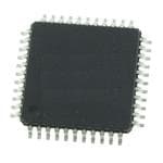
| 描述 | IC CONV R/D 12BIT W/OSC 44-LQFP模数转换器 - ADC IC 12-Bit R/D Cnvtr |
| DevelopmentKit | EVAL-AD2S1205SDZ |
| 产品分类 | |
| 品牌 | Analog Devices Inc |
| 产品手册 | |
| 产品图片 |
|
| rohs | 符合RoHS无铅 / 符合限制有害物质指令(RoHS)规范要求 |
| 产品系列 | 数据转换器IC,模数转换器 - ADC,Analog Devices AD2S1205WSTZ- |
| 数据手册 | |
| 产品型号 | AD2S1205WSTZ |
| 产品目录页面 | |
| 产品种类 | 模数转换器 - ADC |
| 供应商器件封装 | 44-LQFP(7x7) |
| 分辨率 | 12 bit |
| 分辨率(位) | 12 b |
| 包装 | 托盘 |
| 商标 | Analog Devices |
| 安装类型 | 表面贴装 |
| 安装风格 | SMD/SMT |
| 封装 | Tray |
| 封装/外壳 | 44-LQFP |
| 封装/箱体 | LQFP-44 |
| 工作温度 | -40°C ~ 125°C |
| 工作电源电压 | 5 V |
| 工厂包装数量 | 160 |
| 接口类型 | Parallel, Serial |
| 数据接口 | 串行,并联 |
| 最大工作温度 | + 125 C |
| 最小工作温度 | - 40 C |
| 标准包装 | 1 |
| 电压-电源 | 4.75 V ~ 5.25 V |
| 电压源 | 模拟和数字 |
| 类型 | R/D 转换器 |
| 系列 | AD2S1205 |
| 结构 | Resolver to Digital |
| 输入类型 | Differential |
| 通道数量 | 1 Channel |
| 采样率(每秒) | - |


- 商务部:美国ITC正式对集成电路等产品启动337调查
- 曝三星4nm工艺存在良率问题 高通将骁龙8 Gen1或转产台积电
- 太阳诱电将投资9.5亿元在常州建新厂生产MLCC 预计2023年完工
- 英特尔发布欧洲新工厂建设计划 深化IDM 2.0 战略
- 台积电先进制程称霸业界 有大客户加持明年业绩稳了
- 达到5530亿美元!SIA预计今年全球半导体销售额将创下新高
- 英特尔拟将自动驾驶子公司Mobileye上市 估值或超500亿美元
- 三星加码芯片和SET,合并消费电子和移动部门,撤换高东真等 CEO
- 三星电子宣布重大人事变动 还合并消费电子和移动部门
- 海关总署:前11个月进口集成电路产品价值2.52万亿元 增长14.8%


PDF Datasheet 数据手册内容提取
12-Bit RDC with Reference Oscillator AD2S1205 FEATURES FUNCTIONAL BLOCK DIAGRAM Complete monolithic resolver-to-digital converter (RDC) REFERENCE CRYSTAL PINS Parallel and serial 12-bit data ports AD2S1205 S±y1s1t eamrc fmauinltu dteest eocft aioccnu racy EXOCIUTTAPTUIOTNS ORSECF(EDILRALECAN)TCOER REVFOELRTAEGNCEE GIENCNTLEEORRCANTKAOLR Input signal range: 3.15 V p-p ± 27% SYNTHETIC Absolute position and velocity outputs REFERENCE 1250 rps maximum tracking rate, 12-bit resolution Incremental encoder emulation (1024 pulses/rev) RESIONFPLRVUOETMRS AADDCC TYPE II TRACKING LOOP DEFTAEUCLTTION FDOAEUUTTELPCTUTTISON Programmable sinusoidal oscillator on board Single-supply operation (5.00 V ± 5%) POSITION REGISTER VELOCITY REGISTER −40°C to +125°C temperature rating 44-lead LQFP EMEOUNULCTAOPTDUIOETRNS EEMNUCLOADTEIORN MULTIPLEXER 4 kV ESD protection QAuPaPliLfiIeCdA fTorI OauNtoSm otive applications DATA BUS OUTPUT 06339-001 RESET DATA I/O Automotive motion sensing and control Figure 1. Hybrid-electric vehicles Electric power steering Integrated starter generator/alternator Industrial motor control Process control GENERAL DESCRIPTION PRODUCT HIGHLIGHTS The AD2S1205 is a complete 12-bit resolution tracking 1. Ratiometric Tracking Conversion. The Type II tracking resolver-to-digital converter that contains an on-board loop provides continuous output position data without programmable sinusoidal oscillator providing sine wave conversion delay. It also provides noise immunity and excitation for resolvers. tolerance of harmonic distortion on the reference and input signals. The converter accepts 3.15 V p-p ± 27% input signals on the Sin 2. System Fault Detection. A fault detection circuit can sense and Cos inputs. A Type II tracking loop is employed to track the loss of resolver signals, out-of-range input signals, input inputs and convert the input Sin and Cos information into a digital signal mismatch, or loss of position tracking. representation of the input angle and velocity. The maximum 3. Input Signal Range. The Sin and Cos inputs can accept tracking rate is a function of the external clock frequency. The differential input voltages of 3.15 V p-p ± 27%. performance of the AD2S105 is specified across a frequency 4. Programmable Excitation Frequency. Excitation frequency range of 8.192 MHz ± 25%, allowing a maximum tracking rate is easily programmable to 10 kHz, 12 kHz, 15 kHz, or 20 kHz of 1250 rps. by using the frequency select pins (the FS1 and FS2 pins). 5. Triple Format Position Data. Absolute 12-bit angular position data is accessed via either a 12-bit parallel port or a 3-wire serial interface. Incremental encoder emulation is in standard A-quad-B format with direction output available. 6. Digital Velocity Output. 12-bit signed digital velocity accessed via either a 12-bit parallel port or a 3-wire serial interface. Rev. A Information furnished by Analog Devices is believed to be accurate and reliable. However, no responsibility is assumed by Analog Devices for its use, nor for any infringements of patents or other One Technology Way, P.O. Box 9106, Norwood, MA 02062-9106, U.S.A. rights of third parties that may result from its use. Specifications subject to change without notice. No license is granted by implication or otherwise under any patent or patent rights of Analog Devices. Tel: 781.329.4700 www.analog.com Trademarks and registered trademarks are the property of their respective owners. Fax: 781.461.3113 ©2007–2010 Analog Devices, Inc. All rights reserved.
AD2S1205 TABLE OF CONTENTS Features .............................................................................................. 1 False Null Condition .................................................................. 10 Applications ....................................................................................... 1 On-Board Programmable Sinusoidal Oscillator .................... 11 Functional Block Diagram .............................................................. 1 Synthetic Reference Generation ............................................... 11 General Description ......................................................................... 1 Charge-Pump Output ................................................................ 11 Product Highlights ........................................................................... 1 Connecting the Converter ........................................................ 11 Revision History ............................................................................... 2 Clock Requirements ................................................................... 12 Specifications ..................................................................................... 3 Absolute Position and Velocity Output ................................... 12 Absolute Maximum Ratings ............................................................ 5 Parallel Interface ......................................................................... 12 ESD Caution .................................................................................. 5 Serial Interface ............................................................................ 14 Pin Configuration and Function Descriptions ............................. 6 Incremental Encoder Outputs .................................................. 16 Resolver Format Signals ................................................................... 8 Supply Sequencing and Reset ................................................... 16 Theory of Operation ........................................................................ 9 Circuit Dynamics ........................................................................... 17 Fault Detection Circuit ................................................................ 9 Loop Response Model ............................................................... 17 Monitor Signal .............................................................................. 9 Sources of Error .......................................................................... 18 Loss of Signal Detection .............................................................. 9 Connecting to the DSP .............................................................. 19 Signal Degradation Detection .................................................. 10 Outline Dimensions ....................................................................... 20 Loss of Position Tracking Detection ........................................ 10 Ordering Guide .......................................................................... 20 Responding to a Fault Condition ............................................. 10 Automotive Products ................................................................. 20 REVISION HISTORY 5/10—Rev. 0 to Rev. A Changes to Features Section............................................................ 1 Changes to Input Bias Current Parameter and Input Impedance Parameter ...................................................................... 3 Changes to Table 2 ............................................................................ 5 Changes to Loss of Signal Detection Section ................................ 9 Changes to Connecting the Converter Section and Figure 5 ... 11 Change to t Max Value in Table 6 ............................................... 13 6 Changes to t and t Max Values Table 7 .................................... 15 9 10 Changes to Ordering Guide .......................................................... 20 Added Automotive Products Section .......................................... 20 1/07—Revision 0: Initial Version Rev. A | Page 2 of 20
AD2S1205 SPECIFICATIONS AV = DV = 5.0 V ± 5% at −40°C to +125°C, CLKIN = 8.192 MHz ± 25%, unless otherwise noted. DD DD Table 1. Parameter Min Typ Max Unit Conditions/Comments Sin, Cos INPUTS1 Voltage 2.3 3.15 4.0 V p-p Sinusoidal waveforms, Sin − SinLO and Cos − CosLO, differential inputs Input Bias Current 12 μA V = 4.5 V , CLKIN = 10.24 MHz IN DC Input Impedance 0.35 MΩ V = 4.5 V IN DC Common-Mode Voltage 100 mV peak CMV with respect to REFOUT/2 at 10 kHz Phase-Lock Range −44 +44 Degrees Sin/Cos vs. EXC output ANGULAR ACCURACY Angular Accuracy ±11 Arc minutes Zero acceleration, Y grade ±22 Arc minutes Zero acceleration, W grade Resolution 12 Bits Guaranteed no missing codes Linearity INL 2 LSB Zero acceleration, 0 rps to 1250 rps, CLKIN = 10.24 MHz Linearity DNL 0.3 LSB Guaranteed monotonic Repeatability 1 LSB Hysteresis 1 LSB VELOCITY OUTPUT Velocity Accuracy 2 LSB Zero acceleration Resolution 11 Bits Linearity 1 LSB Guaranteed by design, 2 LSB maximum Offset 0 1 LSB Zero acceleration Dynamic Ripple 1 LSB Zero acceleration DYNAMIC PERFORMANCE Bandwidth 1000 2400 Hz Tracking Rate 750 rps CLKIN = 6.144 MHz , guaranteed by design 1000 rps CLKIN = 8.192 MHz , guaranteed by design 1250 rps CLKIN = 10.24 MHz , guaranteed by design Acceleration Error 30 Arc minutes At 10,000 rps, CLKIN = 8.192 MHz Settling Time 179° Step Input 5.2 ms To within ±11 arc minutes, Y grade, CLKIN = 10.24 MHz 4.0 ms To within 1 degree, Y grade, CLKIN = 10.24 MHz EXC, EXC OUTPUTS Voltage 3.34 3.6 3.83 V p-p Load ±100 μA Center Voltage 2.39 2.47 2.52 V Frequency 10 kHz FS1 = high, FS2 = high, CLKIN = 8.192 MHz 12 kHz FS1 = high, FS2 = low, CLKIN = 8.192 MHz 15 kHz FS1 = low, FS2 = high, CLKIN = 8.192 MHz 20 kHz FS1 = low, FS2 = low, CLKIN = 8.192 MHz EXC/EXC DC Mismatch 35 mV THD −58 dB First five harmonics FAULT DETECTION BLOCK Loss of Signal (LOS) Sin/Cos Threshold 2.18 2.24 2.3 V p-p DOS and LOT go low when Sin or Cos fall below threshold Angular Accuracy (Worst Case) 57 Degrees LOS indicated before angular output error exceeds limit (4.0 V p-p input signal and 2.18 V LOS threshold) Angular Latency (Worst Case) 114 Degrees Maximum electrical rotation before LOS is indicated (4.0 V p-p input signal and 2.18 V LOS threshold) Time Latency 125 μs Rev. A | Page 3 of 20
AD2S1205 Parameter Min Typ Max Unit Conditions/Comments Degradation of Signal (DOS) Sin/Cos Threshold 4.0 4.09 4.2 V p-p DOS goes low when Sin or Cos exceeds threshold Angular Accuracy (Worst Case) 33 Degrees DOS indicated before angular output error exceeds limit Angular Latency (Worst Case) 66 Degrees Maximum electrical rotation before DOS is indicated Time Latency 125 μs Sin/Cos Mismatch 385 420 mV DOS latched low when Sin/Cos amplitude mismatch exceeds threshold Loss of Tracking (LOT) Tracking Threshold 5 Degrees LOT goes low when internal error signal exceeds threshold; guaranteed by design Time Latency 1.1 ms Hysteresis 4 Degrees Guaranteed by design VOLTAGE REFERENCE REFOUT 2.39 2.47 2.52 V ±I = 100 μA OUT Drift 70 ppm/°C PSRR −60 dB CHARGE-PUMP OUTPUT (CPO) Frequency 204.8 kHz Square wave output, CLKIN = 8.192 MHz Duty Cycle 50 % POWER SUPPLY I Dynamic 20 mA DD ELECTRICAL CHARACTERISTICS V , Voltage Input Low 0.8 V IL V , Voltage Input High 2.0 V IH V , Voltage Output Low 0.4 V +1 mA load OL V , Voltage Output High 4.0 V −1 mA load OH I , Low Level Input Current −10 +10 μA SAMPLE, CS, RDVEL, CLKIN, SOE pins IL (Non-Pull-Up) I , Low Level Input Current (Pull-Up) −80 +80 μA RD, FS1, FS2, RESET pins IL I , High Level Input Current −10 +10 μA IH I , High Level Three-State Leakage −10 +10 μA OZH I , Low Level Three-State Leakage −10 +10 μA OZL 1 The voltages for Sin, SinLO, Cos, and CosLO relative to AGND must be between 0.2 V and AVDD. Rev. A | Page 4 of 20
AD2S1205 ABSOLUTE MAXIMUM RATINGS Stresses above those listed under Absolute Maximum Ratings Table 2. may cause permanent damage to the device. This is a stress Parameter Rating rating only; functional operation of the device at these or any Supply Voltage (V ) −0.3 V to +7.0 V DD other conditions above those indicated in the operational Supply Voltage (AV ) −0.3 V to +7.0 V DD section of this specification is not implied. Exposure to absolute Input Voltage −0.3 V to V + 0.3 V DD maximum rating conditions for extended periods may affect Output Voltage Swing −0.3 V to V + 0.3 V DD device reliability. Input Current to Any Pin Except Supplies1 ±10 mA Operating Temperature Range (Ambient) −40°C to +125°C ESD CAUTION Storage Temperature Range −65°C to +150°C 1 Transient currents of up to 100 mA do not cause latch-up. Rev. A | Page 5 of 20
AD2S1205 PIN CONFIGURATION AND FUNCTION DESCRIPTIONS T P REFOU REFBY AGND Cos CosLO AVDD SinLO Sin AGND EXC EXC 44 43 42 41 40 39 38 37 36 35 34 DVDD 1 33 RESET RD 2 32 FS2 CS 3 31 FS1 SAMPLE 4 30 LOT RDVEL 5 AD2S1205 29 DOS SOE 6 TOP VIEW 28 DIR (Not to Scale) DB11/SO 7 27 NM DB10/SCLK 8 26 B DB9 9 25 A DB8 10 24 CPO DB7 11 23 DGND 12 13 14 15 16 17 18 19 20 21 22 6 5 4 3 D D 2 1 0 T N DB DB DB DB DGN DVD DB DB DB XTALOU CLKI 06339-002 Figure 2. Pin Configuration Table 3. Pin Function Descriptions Pin No. Mnemonic Description 1, 17 DV Digital Supply Voltage, 4.75 V to 5.25 V. This is the supply voltage for all digital circuitry on the AD2S1205. The DD AV and DV voltages ideally should be at the same potential and must not be more than 0.3 V apart, even DD DD on a transient basis. 2 RD Edge-Triggered Logic Input. This pin acts as a frame synchronization signal and output enable. The output buffer is enabled when CS and RD are held low. 3 CS Chip Select. Active low logic input. The device is enabled when CS is held low. 4 SAMPLE Sample Result. Logic input. Data is transferred from the position and velocity integrators to the position and velocity registers, respectively, after a high-to-low transition on the SAMPLE signal. 5 RDVEL Read Velocity. Logic input. RDVEL input is used to select between the angular position register and the angular velocity register. RDVEL is held high to select the angular position register and low to select the angular velocity register. 6 SOE Serial Output Enable. Logic input. This pin enables either the parallel or serial interface. The serial interface is selected by holding the SOE pin low, and the parallel interface is selected by holding the SOE pin high. 7 DB11/SO Data Bit 11/Serial Data Output Bus. When the SOE pin is high, this pin acts as DB11, a three-state data output pin controlled by CS and RD. When the SOE pin is low, this pin acts as SO, the serial data output bus controlled by CS and RD. The bits are clocked out on the rising edge of SCLK. 8 DB10/SCLK Data Bit 10/Serial Clock. In parallel mode this pin acts as DB10, a three-state data output pin controlled by CS and RD. In serial mode this pin acts as the serial clock input. 9 to 15 DB9 to DB3 Data Bit 9 to Data Bit 3. Three-state data output pins controlled by CS and RD. 16, 23 DGND Digital Ground. These pins are ground reference points for digital circuitry on the AD2S1205. All digital input signals should be referred to this DGND voltage. Both of these pins can be connected to the AGND plane of a system. The DGND and AGND voltages should ideally be at the same potential and must not be more than 0.3 V apart, even on a transient basis. 18 to 20 DB2 to DB0 Data Bit 2 to Data Bit 0. Three-state data output pins controlled by CS and RD. 21 XTALOUT Crystal Output. To achieve the specified dynamic performance, an external crystal is recommended at the CLKIN and XTALOUT pins. The position and velocity accuracy are guaranteed for a frequency range of 8.192 MHz ± 25%. 22 CLKIN Clock Input. To achieve the specified dynamic performance, an external crystal is recommended at the CLKIN and XTALOUT pins. The position and velocity accuracy are guaranteed for a frequency range of 8.192 MHz ± 25%. 24 CPO Charge-Pump Output. Analog output. A 204.8 kHz square wave output with a 50% duty cycle is available at the CPO output pin. This square wave output can be used for negative rail voltage generation or to create a VCC rail. 25 A Incremental Encoder Emulation Output A. Logic output. This output is free running and is valid if the resolver format input signals applied to the converter are valid. Rev. A | Page 6 of 20
AD2S1205 Pin No. Mnemonic Description 26 B Incremental Encoder Emulation Output B. Logic output. This output is free running and is valid if the resolver format input signals applied to the converter are valid. 27 NM North Marker Incremental Encoder Emulation Output. Logic output. This output is free running and is valid if the resolver format input signals applied to the converter are valid. 28 DIR Direction. Logic output. This output is used in conjunction with the incremental encoder emulation outputs. The DIR output indicates the direction of the input rotation and is high for increasing angular rotation. 29 DOS Degradation of Signal. Logic output. Degradation of signal (DOS) is detected when either resolver input (Sin or Cos) exceeds the specified DOS Sin/Cos threshold. See the Signal Degradation Detection section. DOS is indicated by a logic low on the DOS pin and is not latched when the input signals exceed the maximum input level. 30 LOT Loss of Tracking. Logic output. LOT is indicated by a logic low on the LOT pin and is not latched. See the Loss of Signal Detection section. 31 FS1 Frequency Select 1. Logic input. FSI in conjunction with FS2 allows the frequency of EXC/EXC to be programmed. 32 FS2 Frequency Select 2. Logic input. FS2 in conjunction with FS1 allows the frequency of EXC/EXC to be programmed. 33 RESET Reset. Logic input. The AD2S1205 requires an external reset signal to hold the RESET input low until V is within DD the specified operating range of 4.5 V to 5.5 V. See the Supply Sequencing and Reset section. 34 EXC Excitiation Frequency. Analog output. An on-board oscillator provides the sinusoidal excitation signal (EXC) and its complement signal (EXC) to the resolver. The frequency of this reference signal is programmable via the FS1 and FS2 pins. 35 EXC Excitation Frequency Complement. Analog output. An on-board oscillator provides the sinusoidal excitation signal (EXC) and its complement signal (EXC) to the resolver. The frequency of this reference signal is programmable via the FS1 and FS2 pins. 36, 42 AGND Analog Ground. These pins are ground reference points for analog circuitry on the AD2S1205. All analog input signals and any external reference signal should be referred to this AGND voltage. Both of these pins should be connected to the AGND plane of a system. The AGND and DGND voltages should ideally be at the same potential and must not be more than 0.3 V apart, even on a transient basis. 37 Sin Positive Analog Input of Differential Sin/SinLO Pair. The input range is 2.3 V p-p to 4.0 V p-p. 38 SinLO Negative Analog Input of Differential Sin/SinLO Pair. The input range is 2.3 V p-p to 4.0 V p-p. 39 AV Analog Supply Voltage, 4.75 V to 5.25 V. This pin is the supply voltage for all analog circuitry on the AD2S1205. The DD AV and DV voltages ideally should be at the same potential and must not be more than 0.3 V apart, even on a DD DD transient basis. 40 CosLO Negative Analog Input of Differential Cos/CosLO Pair. 41 Cos Positive Analog Input of Differential Cos/CosLO Pair. 43 REFBYP Reference Bypass. Reference decoupling capacitors should be connected here. Typical recommended values are 10 μF and 0.01 μF. 44 REFOUT Voltage Reference Output, 2.39 V to 2.52 V. Rev. A | Page 7 of 20
AD2S1205 RESOLVER FORMAT SIGNALS Vr = Vp × Sin(ωt) Vr= Vp× Sin(ωt) R1 S2 S2 Va = Vs × Sin(ωt) × Cos(θ) R1 Va = Vs × Sin(ωt) × Cos(θ) θ S4 θ S4 R2 R2 S1 S3 S1 S3 Vb = Vs × Sin(ωt) × Sin(θ) Vb = Vs × Sin(ωt) × Sin(θ) (A) CLASSICAL RESOLVER (B)VARIABLE RELUCTANCE RESOLVER 06339-003 Figure 3. Classical Resolver vs. Variable Reluctance Resolver A classical resolver is a rotating transformer that typically has a The stator windings are displaced mechanically by 90° (see primary winding on the rotor and two secondary windings on Figure 3). The primary winding is excited with an ac reference. the stator. A variable reluctance resolver, on the other hand, has the The amplitude of subsequent coupling onto the secondary primary and secondary windings on the stator and no windings windings is a function of the position of the rotor (shaft) on the rotor, as shown in Figure 3; however, the saliency in this relative to the stator. The resolver therefore produces two rotor design provides the sinusoidal variation in the secondary output voltages (S3 − S1, S2 − S4), modulated by the sine and coupling with the angular position. For both designs, the resolver cosine of the shaft angle. Resolver format signals refer to the output voltages (S3 − S1, S2 − S4) are as follows: signals derived from the output of a resolver, as shown in Equation 1. Figure 4 illustrates the output format. S3−S1=E Sin(ωt)×Sinθ (1) 0 S2−S4=E Sin(ωt)×Cosθ 0 where: S2 – S4 θ is the shaft angle. (COSINE) Sin(ωt) is the rotor excitation frequency. E is the rotor excitation amplitude. 0 S3 – S1 (SINE) R2 – R4 (REFERENCE) 06339-004 0° 90° 180° 270° 360° θ Figure 4. Electrical Resolver Representation Rev. A | Page 8 of 20
AD2S1205 THEORY OF OPERATION MONITOR SIGNAL The AD2S1205’s operation is based on a Type II tracking closed- loop principle. The digitally implemented tracking loop continually The AD2S1205 generates a monitor signal by comparing the tracks the position and velocity of the resolver without the need angle in the position register to the incoming Sin and Cos signals for external convert and wait states. As the resolver moves through from the resolver. The monitor signal is created in a similar fashion a position equivalent to the least significant bit weighting, the to the error signal (described in the Theory of Operation section). tracking loop output is updated by 1 LSB. The incoming Sinθ and Cosθ signals are multiplied by the Sin and Cos of the output angle, respectively, and then these values The converter tracks the shaft angle (θ) by producing an output are added together: angle (ϕ) that is fed back and compared with the input angle Monitor=(A1×Sinθ × Sinφ)+(A2×Cosθ×Cosφ) (5) (θ); the difference between the two angles is the error, which is driven towards 0 when the converter is correctly tracking the where: input angle. To measure the error, S3 − S1 is multiplied by Cosϕ A1 is the amplitude of the incoming Sin signal (A1 × Sinθ). and S2 − S4 is multiplied by Sinϕ to give A2 is the amplitude of the incoming Cos signal (A2 × Cosθ). E Sin(ωt)×SinθCosφ for S3 −S1 0 θ is the resolver angle. (2) E Sin(ωt)×CosθSinφ forS2 −S4 ϕ is the angle stored in the position register. 0 The difference is taken, giving Note that Equation 5 is shown after demodulation with the carrier signal Sin(ωt) removed. Also note that for a matched E Sin(ωt)×(SinθCosφ−CosθSinφ) (3) 0 input signal (that is, a no fault condition), A1 is equal to A2. This signal is demodulated using the internally generated When A1 is equal to A2 and the converter is tracking synthetic reference, yielding (therefore, θ is equal to ϕ), the monitor signal output has a E (SinθCosφ−CosθSinφ) (4) constant magnitude of A1 (Monitor = A1 × (Sin2θ + Cos2θ) = A1), 0 which is independent of the shaft angle. When A1 does not Equation 4 is equivalent to ESin(θ − ϕ), which is approximately equal A2, the monitor signal magnitude alternates between A1 0 equal to E(θ − ϕ) for small values of θ − ϕ, where θ − ϕ is the and A2 at twice the rate of the shaft rotation. The monitor 0 angular error. signal is used to detect degradation or loss of input signals. The value E(θ − ϕ) is the difference between the angular error LOSS OF SIGNAL DETECTION 0 of the rotor and the digital angle output of the converter. Loss of signal (LOS) is detected when either resolver input (Sin or Cos) falls below the specified LOS Sin/Cos threshold. The A phase-sensitive demodulator, some integrators, and a compen- AD2S1205 detects this by comparing the monitor signal to a sation filter form a closed-loop system that seeks to null the fixed minimum value. Without the use of external circuitry, error signal. If this is accomplished, ϕ equals the resolver angle, the AD2S1205 can detect the loss of up to three of the four θ, within the rated accuracy of the converter. A Type II tracking connections from the resolver. The addition of two external loop is used so that constant velocity inputs can be tracked 68 kΩ resistors, as outlined in Figure 5, ensures that the loss of without inherent error. all 4 connections, that is, complete removal of the resolver, may For more information about the operation of the converter, see also be detected. LOS is indicated by both DOS and LOT the Circuit Dynamics section. latching as logic low outputs. The DOS and LOT pins are reset to the no fault state by a rising edge of SAMPLE. The FAULT DETECTION CIRCUIT LOS condition has priority over both the DOS and LOT The AD2S1205 fault detection circuit can sense loss of resolver conditions, as shown in Table 4. LOS is indicated within 57° signals, out-of-range input signals, input signal mismatch, or of the angular output error (worst case). loss of position tracking; however, the position indicated by the AD2S1205 may differ significantly from the actual shaft position of the resolver. Rev. A | Page 9 of 20
AD2S1205 SIGNAL DEGRADATION DETECTION RESPONDING TO A FAULT CONDITION Degradation of signal (DOS) is detected when either resolver input If a fault condition (LOS, DOS, or LOT) is indicated by the (Sin or Cos) exceeds the specified DOS Sin/Cos threshold. The AD2S1205, the output data is presumed to be invalid. Even AD2S1205 detects this by comparing the monitor signal to a if a RESET or SAMPLE pulse releases the fault condition and fixed maximum value. In addition, DOS is detected when the is not immediately followed by another fault, the output data amplitudes of the Sin and Cos input signals are mismatched may be corrupted. As discussed previously, there are some fault by more than the specified DOS Sin/Cos mismatch. This is conditions with inherent latency. If the device fault is cleared, identified because the AD2S1205 continuously stores the there may be some latency in the resolver’s mechanical position minimum and maximum magnitude of the monitor signal in before the fault condition is reindicated. internal registers and calculates the difference between these When a fault is indicated, all output pins still provide data, although values. DOS is indicated by a logic low on the DOS pin and is the data may or may not be valid. The fault condition does not not latched when the input signals exceed the maximum input force the parallel, serial, or encoder outputs to a known state. level. When DOS is indicated due to mismatched signals, the output is latched low until a rising edge of SAMPLE resets the Response to specific fault conditions is a system-level requirement. stored minimum and maximum values. The DOS condition has The fault outputs of the AD2S1205 indicate that the device has priority over the LOT condition, as shown in Table 4. DOS is sensed a potential problem with either the internal or external indicated within 33° of the angular output error (worst case). signals of the AD2S1205. It is the responsibility of the system designer to implement the appropriate fault-handling schemes LOSS OF POSITION TRACKING DETECTION within the control hardware and/or algorithm of a given appli- Loss of tracking (LOT) is detected when cation based on the indicated fault(s) and the velocity or position data provided by the AD2S1205. • The internal error signal of the AD2S1205 exceeds 5°. • The input signal exceeds the maximum tracking rate. FALSE NULL CONDITION • The internal position (at the position integrator) differs Resolver-to-digital converters that employ Type II tracking loops from the external position (at the position register) by based on the previously stated error equation (see Equation 4 more than 5°. in the Theory of Operation section) can suffer from a condition known as a false null. This condition is caused by a metastable LOT is indicated by a logic low on the LOT pin and is not solution to the error equation when θ − ϕ = 180°. The AD2S1205 latched. LOT has a 4° hysteresis and is not cleared until the is not susceptible to this condition because its hysteresis is internal error signal or internal/external position mismatch implemented external to the tracking loop. As a result of the is less than 1°. When the maximum tracking rate is exceeded, loop architecture chosen for the AD2S1205, the internal error LOT is cleared only if the velocity is less than the maximum signal constantly has some movement (1 LSB per clock cycle); tracking rate and the internal/external position mismatch is therefore, in a metastable state, the converter moves to an less than 1°. LOT can be indicated for step changes in position unstable condition within one clock cycle. This causes the tracking (such as after a RESET signal is applied to the AD2S1205), or loop to respond to the false null condition as if it were a 180° for accelerations of >~65,000 rps2. It is also useful as a built-in step change in input position (the response time is the same, as test to indicate that the tracking converter is functioning specified in the Dynamic Performance section of Table 1). properly. The LOT condition has lower priority than both the Therefore, it is impossible to enter the metastable condition DOS and LOS conditions, as shown in Table 4. The LOT and after the start-up sequence if the resolver signals are valid. DOS conditions cannot be indicated at the same time. Table 4. Fault Detection Decoding Order of Condition DOS Pin LOT Pin Priority Loss of Signal (LOS) 0 0 1 Degradation of Signal (DOS) 0 1 2 Loss of Tracking (LOT) 1 0 3 No Fault 1 1 Rev. A | Page 10 of 20
AD2S1205 ON-BOARD PROGRAMMABLE SINUSOIDAL zero crossing of either the Sin or Cos (whichever signal is OSCILLATOR larger), which improves phase accuracy, and evaluating the phase of the resolver reference excitation. The synthetic reference reduces An on-board oscillator provides the sinusoidal excitation signal the phase shift between the reference and Sin/Cos inputs to less (EXC) and its complement signal (EXC) to the resolver. The fre- than 10° and can operate for phase shifts of ±45°. quency of this reference signal is programmable to four standard frequencies (10 kHz, 12 kHz, 15 kHz, or 20 kHz) by using the CHARGE-PUMP OUTPUT FS1 and FS2 pins (see Table 5). FS1 and FS2 have internal pull-ups, A 204.8 kHz square wave output with a 50% duty cycle is available so the default frequency is 10 kHz. The amplitude of this signal at the CPO pin of the AD2S1205. This square wave output can is centered on 2.5 V and has an amplitude of 3.6 V p-p. be used for negative rail voltage generation or to create a V rail. CC Table 5. Excitation Frequency Selection CONNECTING THE CONVERTER Frequency Selection (kHz) FS1 FS2 Ground is connected to the AGND and DGND pins (see Figure 5). 10 1 1 A positive power supply (V ) of 5 V dc ± 5% is connected to DD 12 1 0 the AV and DV pins, with typical values for the decoupling DD DD 15 0 1 capacitors being 10 nF and 4.7 μF. These capacitors are then 20 0 0 placed as close to the device pins as possible and are connected to both AV and DV . If desired, the reference oscillator DD DD The frequency of the reference signal is a function of the CLKIN frequency can be changed from the nominal value of 10 kHz frequency. By decreasing the CLKIN frequency, the minimum using FS1 and FS2. Typical values for the oscillator decoupling excitation frequency can also be decreased. This allows an capacitors are 20 pF, whereas typical values for the reference excitation frequency of 7.5 kHz to be set when using a CLKIN decoupling capacitors are 10 μF and 0.01 μF. As outlined in the frequency of 6.144 MHz, and it also decreases the maximum Loss of Signal Detection section 68 kΩ resistors between the Sin tracking rate to 750 rps. and SinLO inputs and the Cos and CosLO inputs can be used to ensure loss of signal detection when all four inputs from resolver The reference output of the AD2S1205 requires an external buffer are disconnected. amplifier to provide gain and additional current to drive the resolver. See Figure 6 for a suggested buffer circuit. In this recommended configuration, the converter introduces a V /2 offset in the Sin and Cos signal outputs from the resolver. REF The AD2S1205 also provides an internal synchronous reference The SinLO and CosLO signals can each be connected to a different signal that is phase locked to its Sin and Cos inputs. Phase errors potential relative to ground if the Sin and Cos signals adhere to the between the resolver’s primary and secondary windings may recommended specifications. Note that because the EXC and EXC degrade the accuracy of the RDC and are compensated for by using outputs are differential, there is an inherent gain of 2×. Figure 6 this synchronous reference signal. This also compensates for the shows a suggested buffer circuit. Capacitor C1 may be used in phase shifts due to temperature and cabling, and it eliminates the parallel with Resistor R2 to filter out any noise that may exist on the need for an external preset phase-compensation circuit. EXC and EXC outputs. Care should be taken when selecting the SYNTHETIC REFERENCE GENERATION cutoff frequency of this filter to ensure that phase shifts of the carrier caused by the filter do not exceed the phase lock range When a resolver undergoes a high rotation rate, the RDC tends of the AD2S1205. to act as an electric motor and produces speed voltages in addition to the ideal Sin and Cos outputs. These speed voltages are The gain of the circuit is in quadrature to the main signal waveform. Moreover, nonzero CarrierGain=−(R2/R1)×(1/(1+R2×C1×ω)) (7) resistance in the resolver windings causes a nonzero phase shift between the reference input and the Sin and Cos outputs. The and combination of the speed voltages and the phase shift causes a tracking error in the RDC that is approximated by V =⎜⎛V ×⎜⎛1+R2⎟⎞⎟⎞−⎜⎛R2×(1/(1+R2×C1×ω))V ⎟⎞ (8) OUT ⎝ REF ⎝ R1⎠⎠ ⎝R1 IN⎠ RotationRate Error=PhaseShift× (6) ReferenceFrequency where: ω is the radian frequency of the applied signal. To compensate for the described phase error between the resolver V , a dc voltage, is set so that V is always a positive value, reference excitation and the Sin/Cos signals, an internal synthetic REF OUT eliminating the need for a negative supply. reference signal is generated in phase with the reference frequency carrier. The synthetic reference is derived using the internally filtered Sin and Cos signals. It is generated by determining the Rev. A | Page 11 of 20
AD2S1205 A separate screened twisted pair cable is recommended for CLOCK REQUIREMENTS analog inputs Sin/SinLO and Cos/CosLO. The screens should To achieve the specified dynamic performance, an external crystal terminate to either REFOUT or AGND. is recommended at the CLKIN and XTALOUT pins. The position S2 S3 R2 and velocity accuracy are guaranteed for a frequency range of 8.192 MHz ± 25%. However, the velocity outputs are scaled in R1 proportion to the clock frequency so that if the clock is 25% S4 S1 greater than the nominal, the full-scale velocity is 25% greater than 5V BUFFER BUFFER nominal. The maximum tracking rate, tracking loop bandwidth, 4.7μF CIRCUIT CIRCUIT and excitation frequency also vary with the clock frequency. 10nF 10nF 10μF 68kΩ 68kΩ ABSOLUTE POSITION AND VELOCITY OUTPUT The angular position and velocity are represented by binary data 44 43 42 41 40 39 38 37 36 35 34 and can be extracted via either a 12-bit parallel interface or a P D s O D O n D C C 5V 1 DVDD EFBY AGN Co CosL AVD SinL Si AGN EX EX 33 RESET 3-wire serial interface that operates at clock rates of up to 25 MHz. 2 R 32 SOE Input 3 31 The serial output enable pin (SOE) is held high to enable the 4 30 5 29 parallel interface and low to enable the serial interface. In the 6 AD2S1205 28 latter case, Pin DB0 to Pin DB9 are placed into a high impedance 7 27 state while DB11 is the serial output (SO) and DB10 is the serial 8 26 clock input (SCLK). 9 25 Data Format 10 24 11 GND VDD DGND 23 The angular position data represents the absolute position of D D 12 13 14 15 16 17 18 19 20 21 22 the resolver shaft as a 12-bit unsigned binary word. The angular 5V velocity data is a 12-bit twos complement word, representing 8.192 MHz the velocity of the resolver shaft rotating in either a clockwise 4.7μF 10nF or counterclockwise direction. 20pF 20pF 06339-005 PARALLEL INTERFACE Figure 5. Connecting the AD2S1205 to a Resolver The angular position and velocity are available on the AD2S1205 in two 12-bit registers, accessed via the 12-bit parallel port. The C1 parallel interface is selected by holding the SOE pin high. Data is transferred from the velocity and position integrators to the R2 12V position and velocity registers, respectively, after a high-to-low 12V transition on the SAMPLE pin. The RDVEL pin selects whether R1 EXC/EXC data from the position or velocity register is transferred to the (VIN) (VREF) AD8662 VOUT output register. The CS pin must be held low to transfer data from the selected register to the output register. Finally, the RD 5V 06339-017 iennpaubtl eis t uhsee odu ttop uret abdu tfhfeer .d Tahtae ftriommin tgh ere oquutipruemt reengtiss tfeorr a tnhde troea d Figure 6. Buffer Circuit cycle are shown in Figure 7. SAMPLE Input Data is transferred from the position and velocity integrators to the position and velocity registers, respectively, after a high-to- low transition on the SAMPLE signal. This pin must be held low for at least t to guarantee correct latching of the data. RD 1 should not be pulled low before this time because data will not be ready. The converter continues to operate during the read process. A rising edge of SAMPLE resets the internal registers that contain the minimum and maximum magnitude of the monitor signal. Rev. A | Page 12 of 20
AD2S1205 CS Input RD Input The 12-bit data bus lines are normally in a high impedance The device is enabled when CS is held low. state. The output buffer is enabled when CS and RD are held RDVEL Input low. A falling edge of the RD signal transfers data to the output RDVEL input is used to select between the angular position buffer. The selected data is made available to the bus to be read register and the angular velocity register, as shown in Figure 7. within t6 of the RD pin going low. The data pins return to a high RDVEL is held high to select the angular position register and impedance state when the RD pin returns to a high state within low to select the angular velocity register. The RDVEL pin must t7. When reading data continuously, wait a minimum of t3 after be set (stable) at least t before the RD pin is pulled low. RD is released before reapplying it. 4 f CLKIN CLKIN t1 t1 SAMPLE t 2 CS t 3 t 3 RD t5 t5 RDVEL t4 t4 DATA POSITION VELOCITY t DON'T CARE t6 7 t6 t7 06339-007 Figure 7. Parallel Port Read Timing Table 6. Parallel Port Timing Parameter Description Min Typ Max Unit f Frequency of clock input 6.144 8.192 10.24 MHz CLKIN t SAMPLE pulse width 2 × (1/f ) + 20 ns 1 CLKIN t Delay from SAMPLE before RD/CS low 6 × (1/f ) + 20 ns 2 CLKIN t RD pulse width 18 ns 3 t Set time RDVEL before RD/CS low 5 ns 4 t Hold time RDVEL after RD/CS low 7 ns 5 t Enable delay RD/CS low to data valid 30 ns 6 t Disable delay RD/CS low to data high-Z 18 ns 7 Rev. A | Page 13 of 20
AD2S1205 SERIAL INTERFACE SAMPLE Input Data is transferred from the position and velocity integrators to The angular position and velocity are available on the AD2S1205 the position and velocity registers, respectively, after a high-to- in two 12-bit registers. These registers can be accessed via a 3-wire serial interface (SO, RD, and SCLK) that operates at clock rates low transition on the SAMPLE signal. This pin must be held low of up to 25 MHz and is compatible with SPI and DSP interface for at least t1 to guarantee correct latching of the data. RD should standards. The serial interface is selected by holding the SOE pin not be pulled low before this time because data will not be ready. The converter continues to operate during the read process. low. Data from the position and velocity integrators are first trans- ferred to the position and velocity registers using the SAMPLE pin. CS Input The RDVEL pin selects whether data is transferred from the The device is enabled when CS is held low. position or velocity register to the output register, and the CS pin must be held low to transfer data from the selected register to the RD Input output register. Finally, the RD input is used to read the data that The 12-bit data bus lines are normally in a high impedance is clocked out of the output register and is available on the serial state. The output buffer is enabled when CS and RD are held output pin (SO). When the serial interface is selected, DB11 is used low. The RD input is an edge-triggered input that acts as a frame as the serial output pin (SO), DB10 is used as the serial clock input synchronization signal and an output enable. On a falling edge of (SCLK), and Pin DB0 to Pin DB9 are placed into the high imped- the RD signal, data is transferred to the output buffer. Data is ance state. The timing requirements for the read cycle are described then available on the serial output pin (SO); however, it is only in Figure 8. valid after RD is held low for t. The serial data is clocked out 9 SO Output of the SO pin on the rising edges of SCLK, and each data bit is The output shift register is 16 bits wide. Data is clocked out of available at the SO pin on the falling edge of SCLK. However, the device as a 16-bit word by the serial clock input (SCLK). as the MSB is clocked out by the falling edge of RD, the MSB is The timing diagram for this operation is shown in Figure 8. available at the SO pin on the first falling edge of SCLK. Each The 16-bit word consists of 12 bits of angular data (position or subsequent bit of the data-word is shifted out on the rising edge velocity, depending on RDVEL input), one RDVEL status bit, of SCLK and is available at the SO pin on the falling edge of and three status bits (a parity bit, a degradation of signal bit, and SCLK for the next 15 clock pulses. a loss of tracking bit). Data is clocked out MSB first from the The high-to-low transition of RD must occur during the high SO pin, beginning with DB15. DB15 through DB4 correspond time of the SCLK to avoid DB14 being shifted on the first rising to the angular information. The angular position data format edge of the SCLK, which would result in the MSB being lost. is unsigned binary, with all 0s corresponding to 0° and all 1s cor- RD may rise high after the last falling edge of SCLK. If RD is responding to 360° − l LSB. The angular velocity data format held low and additional SCLKs are applied after DB0 has been is twos complement, with the MSB representing the rotation read, then 0s will be clocked from the data output. When direction. DB3 is the RDVEL status bit, with a 1 indicating reading data continuously, wait a minimum of t after RD position and a 0 indicating velocity. DB2 is DOS, the degradation 5 is released before reapplying it. of signal flag (refer to the Fault Detection Circuit section). Bit 1 is LOT, the loss of tracking flag (refer to the Fault Detection RDVEL Input Circuit section). Bit 0 is PAR, the parity bit. The position and RDVEL input is used to select between the angular position velocity data are in odd parity format, and the data readback register and the angular velocity register. RDVEL is held high to always contains an odd number of logic highs (1s). select the angular position register and low to select the angular velocity register. The RDVEL pin must be set (stable) at least t 4 before the RD pin is pulled low. Rev. A | Page 14 of 20
AD2S1205 f CLKIN CLKIN t1 t1 SAMPLE t 2 CS t 3 t 3 RD t5 t5 RDVEL t4 t4 t 6 t6 t7 t7 SO POSITION VELOCITY t 8 RD t SCLK SCLK t10 t11 SO MSB MSB – 1 LSB RDVEL DOS LOT PAR t9 06339-008 Figure 8. Serial Port Read Timing Table 7. Serial Port Timing1 Parameter Description Min Typ Max Unit t8 MSB read time RD/CS to SCLK 15 tSCLK ns t SO enable time RD/CS to DB valid 30 ns 9 t Data access time, SCLK to DB valid 30 ns 10 t Bus relinquish time RD/CS to SO high-Z 18 ns 11 t Serial clock period (25 MHz maximum) 40 ns SCLK 1 t1 to t7 are as defined in Table 6. Rev. A | Page 15 of 20
AD2S1205 INCREMENTAL ENCODER OUTPUTS To achieve the maximum speed of 75,000 rpm, select an external CLKIN of 10.24 MHz to produce an internal clock The A, B, and NM incremental encoder emulation outputs are frequency equal to 5.12 MHz. free running and are valid if the resolver format input signals applied to the converter are valid. This compares favorably with encoder specifications, which state f as 20 kHz (photo diodes) to 125 kHz (laser based), MAX The AD2S1205 emulates a 1024-line encoder, meaning that, in depending on the type of light system used. A 1024-line laser- terms of the converter resolution, one revolution produces 1024 A based encoder has a maximum speed of 7300 rpm. and B pulses. Pulse A leads Pulse B for increasing angular rotation (clockwise direction). The addition of the DIR output negates The inclusion of A and B outputs allows an AD2S1205 and the need for external A and B direction decode logic. The DIR resolver-based solution to replace optical encoders directly output indicates the direction of the input rotation and is high without the need to change or upgrade the user’s existing for increasing angular rotation. DIR can be considered an asyn- application software. chronous output that can make multiple changes in state between SUPPLY SEQUENCING AND RESET two consecutive LSB update cycles. This occurs when the direction of the rotation of the input changes but the magnitude of the The AD2S1205 requires an external reset signal to hold the rotation is less than 1 LSB. RESET input low until V is within the specified operating DD range of 4.5 V to 5.5 V. The north marker pulse is generated as the absolute angular position passes through zero. The north marker pulse width is The RESET pin must be held low for a minimum of 10 μs after set internally for 90° and is defined relative to the A cycle. V is within the specified range (shown as t in Figure 10). DD RST Figure 9 details the relationship between A, B, and NM. Applying a RESET signal to the AD2S1205 initializes the output position to a value of 0x000 (degrees output through the parallel, serial, and encoder interfaces) and causes LOS to be indicated A (LOT and DOS pins pulled low), as shown in Figure 10. Failure to apply the correct power-up/reset sequence may result B in an incorrect position indication. After a rising edge on the RESET input, the device must be NM 06339-009 ainlltoewrneadl acti rlceuaisttr 2y0 t om sst a(bshiloizwen a nasd ttThReAC tKr ainck Finiggu lroeo 1p0 )to f osre ttthlee to Figure 9. A, B, and NM Timing for Clockwise Rotation the step change of the input position. After t , a SAMPLE TRACK pulse must be applied, which in turn releases the LOT and DOT Unlike incremental encoders, the AD2S1205 encoder output is pins to the state determined by the fault detection circuitry and not subject to error specifications such as cycle error, eccentricity, provides valid position data at the parallel and serial outputs. pulse and state width errors, count density, and phase ϕ. The (Note that if position data is acquired via the encoder outputs, maximum speed rating (n) of an encoder is calculated from its it can be monitored during t .) maximum switching frequency (f ) and its pulses per revo- TRACK MAX lution (PPR). The RESET pin is then internally pulled up. 60×f n= MAX (9) PPR VDD 4.75V The A and B pulses of the AD2S1205 are initiated from the inter- ttRRSSTT nal clock frequency, which is exactly half the external CLKIN RESET t TRACK frequency. With a nominal CLKIN frequency of 8.192 MHz, the internal clock frequency is 4.096 MHz. The equivalent SAMPLE encoder switching frequency is 1/4×4.096 MHz=1.024 MHz(4Updates=1Pulse) (10) LOT VALID For 12 bits, the PPR is 1024. Therefore, the maximum speed (n) OUTPUT DATA of the AD2S1205 with a CLKIN of 8.192 MHz is DOS n=60×1,024,000=60,000rpm (11) 06339-010 1024 Figure 10. Power Supply Sequencing and Reset Rev. A | Page 16 of 20
AD2S1205 CIRCUIT DYNAMICS LOOP RESPONSE MODEL R2D open-loop transfer function ERROR (ACCELERATION) VELOCITY G(z)=k1×k2×I(z)2×C(z) (19) c 1 – az–1 c R2D closed-loop transfer function θIN k1 × k2 1 – z–1 1 – bz–1 1 – z–1 θOUT – G(z) Sin/Cos LOOKUP 06339-011 H(z)=1+G(z) (20) Figure 11. RDC System Response Block Diagram The closed-loop magnitude and phase responses are that of a second-order low-pass filter (see Figure 12 and Figure 13). The RDC is a mixed-signal device that uses two ADCs to digitize signals from the resolver and a Type II tracking loop To convert G(z) into the s-plane, an inverse bilinear transfor- to convert these to digital position and velocity words. mation is performed by substituting the following equation for z: The first gain stage consists of the ADC gain on the Sin/Cos inputs and the gain of the error signal into the first integrator. 2 +s The first integrator generates a signal proportional to velocity. t z= (21) The compensation filter contains a pole and a zero that are used 2 −s to provide phase margin and reduce high frequency noise gain. t The second integrator is the same as the first and generates the where t is the sampling period (1/4.096 MHz ≈ 244 ns). position output from the velocity signal. The Sin/Cos lookup has unity gain. The values for each section are as follows: Substitution yields the open-loop transfer function G(s). ADC gain parameter (k1NOM = 1.8/2.5) 1+st+s2t2 1+s×t(1+a) V (V ) G(s)= k1×k2(1−a)× 4 × 2(1−a) (22) k2= IN p (12) a−b s2 t(1+b) V (V) 1+s× REF 2(1−b) Error gain parameter This transformation produces the best matching at low frequencies k2=18 ×106×2π (13) (f < fSAMPLE). At such frequencies (within the closed-loop bandwidth of the AD2S1205), the transfer function can be simplified to Compensator zero coefficient K 1+st G(s)≅ a × 1 (23) 4095 s2 1+st a= (14) 2 4096 where: Compensator pole coefficient t(1+a) t = 4085 1 2(1−a) b= (15) 4096 t(1+b) t = Integrator gain parameter 2 2(1−b) k1×k2(1−a) 1 K = c= (16) a a−b 4,096,000 INT1 and INT2 transfer function Solving for each value gives t1 = 1 ms, t2 = 90 μs, and Ka ≈ 7.4 × 10⁶ s−2. Note that the closed-loop response is described as c I(z)= (17) 1−z−1 G(s) H(s)= (24) 1+G(s) Compensation filter transfer function By converting the calculation to the s-domain, it is possible to 1−az−1 C(z)= (18) quantify the open-loop dc gain (K). This value is useful to 1−bz−1 a calculate the acceleration error of the loop (see the Sources of Error section). Rev. A | Page 17 of 20
AD2S1205 The step response to a 10° input step is shown in Figure 14. SOURCES OF ERROR Because the error calculation (see Equation 2) is nonlinear for Acceleration large values of θ − ϕ, the response time for such large (90° to A tracking converter employing a Type II servo loop does not 180°) step changes in position typically takes three times as long have a lag in velocity. There is, however, an error associated as the response to a small (<20°) step change in position. In with acceleration. This error can be quantified using the response to a step change in velocity, the AD2S1205 exhibits acceleration constant (K) of the converter. the same response characteristics as it does for a step change a in position. Input Acceleration K = (25) a Tracking Error 5 0 Conversely, –5 InputAcceleration –10 Tracking Error= (26) E (dB)–15 Ka UD–20 Figure 15 shows tracking error vs. acceleration for the AD2S1205. T NI G–25 A The units of the numerator and denominator must be consistent. M –30 The maximum acceleration of the AD2S1205 is defined as the –35 acceleration that creates an output position error of 5° (that is, ––4405 06339-012 wcahlceunl LatOedT aiss indicated). The maximum acceleration can be 1 10 100 1k 10k 100k FREQUENCY (Hz) MaximumAcceleration= Ka(sec−2)×5° ≅103,000 rps2 (27) Figure 12. RDC System Magnitude Response 360(°/rev) 0 10 –20 9 –40 8 s) e grees) ––8600 R (Degre 67 ASE (De––112000 G ERRO 45 H N P–140 CKI 3 A R –160 T 2 ––1280001 10 100 1k 10k 100k06339-013 010 40k 80k 120k 160k 200k06339-015 FREQUENCY (Hz) ACCELERATION (rps2) Figure 13. RDC System Phase Response Figure 15. Tracking Error vs. Acceleration 20 18 16 14 s) ee 12 gr e D 10 E ( L G 8 N A 6 4 02 06339-014 0 1 2 3 4 5 TIME (ms) Figure 14. RDC Small Step Response Rev. A | Page 18 of 20
AD2S1205 CONNECTING TO THE DSP and RDVEL can be obtained using two PIO outputs of the ADMC401. The 12 bits of significant data and the status bits The AD2S1205 serial port is ideally suited for interfacing to DSP- are available on each consecutive negative edge of the clock configured microprocessors. Figure 16 shows the AD2S1205 after the RD signal goes low. Data is clocked from the AD2S1205 interfaced to an ADMC401, one of the DSP-based motor into the data receive register of the ADMC401. This is internally controllers. set to 16 bits (12 data bits, 4 status bits) because 16 bits are The on-chip serial port of the ADMC401 is used in the following received overall. The serial port automatically generates an configuration internal processor interrupt. This allows the ADMC401 to read all 16 bits and then continue to process data. • Alternate framing transmit mode with internal framing (internally inverted) All ADMC401 products can interface to the AD2S1205 by using • Normal framing receive mode with external framing similar interface circuitry. (internally inverted) • Internal serial clock generation ADMC401 AD2S1205 SCLK SCLK SOE In this configuration, the internal TFS signal of ADMC401 DR SO is used as an external RFS to fully control the timing of TFS RD data received, and the same TFS is connected to RD of the RFS AD2S1205. In addition, the ADMC401 provides an internal continuous serial clock to the AD2S1205. The SAMPLE signal PWMSYNC SAMPLE on the AD2S1205 can be provided either by using a PIO or by PIO CS iannvde rvteilnogc itthye r PeaWdiMngSsY wNiCth stihgen aPlW toM sy snwcihtrcohninizge f trheqe upeonscityi.o CnS PIO RDVEL 06339-016 Figure 16. Connecting to the ADMC401 Rev. A | Page 19 of 20
AD2S1205 OUTLINE DIMENSIONS 12.20 0.75 1.60 12.00 SQ 0.60 MAX 11.80 0.45 44 34 1 33 PIN 1 10.20 TOP VIEW 10.00 SQ (PINS DOWN) 9.80 1.45 0.20 1.40 0.09 1.35 7° 3.5° 11 23 00..1055 SEATING 0.10 0° 12 22 PLANE COPLANARITY VIEW A 0.80 0.45 BSC 0.37 VIEW A LEAD PITCH 0.30 ROTATED 90° CCW COMPLIANTTO JEDEC STANDARDS MS-026-BCB 051706-A Figure 17. 44-Lead Low Profile Quad Flat Package [LQFP] (ST-44-1) Dimensions shown in millimeters ORDERING GUIDE Model1, 2 Temperature Range Angular Accuracy Package Description Package Option AD2S1205YSTZ −40°C to +125°C ±11 arc min 44-Lead Low Profile Quad Flat Package [LQFP] ST-44-1 ADW71205YSTZ −40°C to +125°C ±11 arc min 44-Lead Low Profile Quad Flat Package [LQFP] ST-44-1 AD2S1205WSTZ −40°C to +125°C ±22 arc min 44-Lead Low Profile Quad Flat Package [LQFP] ST-44-1 ADW71205WSTZ −40°C to +125°C ±22 arc min 44-Lead Low Profile Quad Flat Package [LQFP] ST-44-1 ADW71205WSTZ-RL −40°C to +125°C ±22 arc min 44-Lead Low Profile Quad Flat Package [LQFP] ST-44-1 EVAL-AD2S1205CBZ3 Evaluation Board EVAL-CONTROL BRD24 Controller Board 1 Z = RoHS Compliant Part. 2 W = Qualified for Automotive Applications. 3 This can be used either as a standalone evaluation board or in conjunction with the evaluation board controller for evaluation/demonstration purposes. 4 Evaluation board controller. This board is a complete unit that allows a PC to control and communicate with all Analog Devices evaluation boards ending in the CB designator. For a complete evaluation kit, order the ADC evaluation board (that is, the EVAL-AD2S1205CBZ), the EVAL-CONTROL BRD2, and a 12 V ac transformer. AUTOMOTIVE PRODUCTS The AD2S1205 models are available with controlled manufacturing to support the quality and reliability requirements of automotive applications. Note that these automotive models may have specifications that differ from the commercial models; therefore, designers should review the Specifications section of this data sheet carefully. Only the automotive grade products shown are available for use in automotive applications. Contact your local Analog Devices account representative for specific product ordering information and to obtain the specific Automotive Reliability reports for these models. ©2007–2010 Analog Devices, Inc. All rights reserved. Trademarks and registered trademarks are the property of their respective owners. D06339-0-5/10(A) Rev. A | Page 20 of 20
Mouser Electronics Authorized Distributor Click to View Pricing, Inventory, Delivery & Lifecycle Information: A nalog Devices Inc.: AD2S1205WSTZ ADW71205YSTZ EVAL-AD2S1205SDZ ADW71205WSTZ AD2S1205YSTZ ADW71205WSTZ-RL ADW71205YSTZ-RL