ICGOO在线商城 > 集成电路(IC) > 数据采集 - ADCs/DAC - 专用型 > AD7401AYRWZ
 Datasheet下载
- 型号: AD7401AYRWZ
- 制造商: Analog
- 库位|库存: xxxx|xxxx
- 要求:
| 数量阶梯 | 香港交货 | 国内含税 |
| +xxxx | $xxxx | ¥xxxx |
查看当月历史价格
查看今年历史价格
AD7401AYRWZ产品简介:
ICGOO电子元器件商城为您提供AD7401AYRWZ由Analog设计生产,在icgoo商城现货销售,并且可以通过原厂、代理商等渠道进行代购。 AD7401AYRWZ价格参考。AnalogAD7401AYRWZ封装/规格:数据采集 - ADCs/DAC - 专用型, 隔离模块 16 b 串行 16-SOIC。您可以下载AD7401AYRWZ参考资料、Datasheet数据手册功能说明书,资料中有AD7401AYRWZ 详细功能的应用电路图电压和使用方法及教程。
AD7401AYRWZ 是由 Analog Devices Inc.(ADI)生产的一款专用型数据采集芯片,属于 AD7401 系列隔离式Σ-Δ调制器。其主要应用场景包括:

1. 工业自动化与控制
   AD7401AYRWZ 可用于工业自动化系统中的信号隔离和数据采集。例如,在电机控制、过程控制或传感器监测中,它能够将来自电流互感器或其他传感器的模拟信号转换为数字信号,并通过磁隔离技术防止噪声干扰和高压损坏。

2. 电力监测与保护
   在电力系统中,这款芯片常用于电流和电压的精确测量。它可以通过隔离接口连接到电流互感器(CT)或 Rogowski 线圈,实现对电网参数的实时监控,同时提供电气隔离以确保安全。

3. 能源管理
   AD7401AYRWZ 适用于智能电表和其他能源管理系统。它可以准确地测量电流和功率,支持低功耗设计,并通过隔离功能提高系统的可靠性和抗干扰能力。

4. 医疗设备
   在某些需要高精度和电气隔离的医疗应用中,例如患者监护仪或生命体征检测设备,该芯片可以用来采集生物电信号,同时保护患者免受高压危险。

5. 汽车电子
   该芯片可用于电动汽车(EV)或混合动力汽车(HEV)的动力系统中,例如电池管理、电机控制或电流监测。它的高隔离性能有助于在恶劣环境下稳定运行。

6. 通信基础设施
   在通信基站或电源模块中,AD7401AYRWZ 可以用于监测电源状态或负载电流,确保系统的高效运行并提供故障保护。

总结来说,AD7401AYRWZ 的核心优势在于其高精度、低延迟的Σ-Δ调制技术和强大的电气隔离能力,这使其非常适合需要信号隔离和高可靠性数据采集的应用场景。
| 参数 | 数值 |
| 产品目录 | 集成电路 (IC)半导体 |
| 描述 | IC MODULATOR SIGMA-DELTA 16SOIC模数转换器 - ADC Isolated Modulator |
| DevelopmentKit | EVAL-AD7401AEDZ |
| 产品分类 | |
| 品牌 | Analog Devices Inc |
| 产品手册 | |
| 产品图片 |
|
| rohs | 符合RoHS无铅 / 符合限制有害物质指令(RoHS)规范要求 |
| 产品系列 | 数据转换器IC,模数转换器 - ADC,Analog Devices AD7401AYRWZiCoupler® |
| 数据手册 | |
| 产品型号 | AD7401AYRWZ |
| 产品目录页面 | |
| 产品种类 | 模数转换器 - ADC |
| 位数 | 16 |
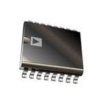
| 供应商器件封装 | 16-SOIC W |
| 信噪比 | 83 dB |
| 分辨率 | 16 bit |
| 包装 | 管件 |
| 商标 | Analog Devices |
| 安装类型 | 表面贴装 |
| 安装风格 | SMD/SMT |
| 封装 | Tube |
| 封装/外壳 | 16-SOIC(0.295",7.50mm 宽) |
| 封装/箱体 | SOIC-16 |
| 工作温度 | -40°C ~ 125°C |
| 工作电源电压 | 5 V |
| 工厂包装数量 | 47 |
| 接口类型 | Serial |
| 数据接口 | 串行 |
| 最大功率耗散 | 85 W |
| 最大工作温度 | + 125 C |
| 最小工作温度 | - 40 C |
| 标准包装 | 47 |
| 特性 | - |
| 电压参考 | Internal |
| 电压源 | 单电源 |
| 系列 | AD7401A |
| 结构 | Sigma-Delta |
| 视频文件 | http://www.digikey.cn/classic/video.aspx?PlayerID=1364138032001&width=640&height=505&videoID=2245193158001 |
| 转换器数 | 1 |
| 转换器数量 | 1 |
| 转换速率 | 20 MS/s |
| 输入数和类型 | 1 个单端,双极 |
| 输入类型 | Differential |
| 通道数量 | 1 Channel |
| 采样率(每秒) | 20M |


- 商务部:美国ITC正式对集成电路等产品启动337调查
- 曝三星4nm工艺存在良率问题 高通将骁龙8 Gen1或转产台积电
- 太阳诱电将投资9.5亿元在常州建新厂生产MLCC 预计2023年完工
- 英特尔发布欧洲新工厂建设计划 深化IDM 2.0 战略
- 台积电先进制程称霸业界 有大客户加持明年业绩稳了
- 达到5530亿美元!SIA预计今年全球半导体销售额将创下新高
- 英特尔拟将自动驾驶子公司Mobileye上市 估值或超500亿美元
- 三星加码芯片和SET,合并消费电子和移动部门,撤换高东真等 CEO
- 三星电子宣布重大人事变动 还合并消费电子和移动部门
- 海关总署:前11个月进口集成电路产品价值2.52万亿元 增长14.8%


PDF Datasheet 数据手册内容提取
Isolated Sigma-Delta Modulator Data Sheet AD7401A FEATURES GENERAL DESCRIPTION 20 MHz maximum external clock rate The AD7401A1 is a second-order, sigma-delta (Σ-Δ) modulator Second-order modulator that converts an analog input signal into a high speed, 1-bit data 16 bits, no missing codes stream with on-chip digital isolation based on the Analog ±2 LSB INL typical at 16 bits Devices, Inc., iCoupler® technology. The AD7401A operates 1 µV/°C typical offset drift from a 5 V power supply and accepts a pseudo-differential input On-board digital isolator signal of ±250 mV (±320 mV full scale). The analog input is On-board reference continuously sampled by the analog modulator, eliminating the ±250 mV analog input range need for external sample-and-hold circuitry. The input Low power operation: 17 mA typical at 5.5 V information is contained in the output stream as a density of −40°C to +125°C operating range ones with a data rate of up to 20 MHz. The original information 16-lead SOIC package can be reconstructed with an appropriate digital filter. The Internal clock version: AD7400A serial I/O can use a 5 V or a 3.3 V supply (V ). DD2 Safety and regulatory approvals The serial interface is digitally isolated. High speed CMOS, UL recognition combined with Analog Devices, Inc., iCoupler® technology , 5000 V rms for 1 minute per UL 1577 means the on-chip isolation provides outstanding performance CSA Component Acceptance Notice #5A characteristics, superior to alternatives such as optocoupler VDE Certificate of Conformity devices. The device contains an on-chip reference. The DIN V VDE V 0884-10 (VDE V 0884-10):2006-12 AD7401A is offered in a 16-lead SOIC and has an operating V = 891 V peak IORM temperature range of −40°C to +125°C. Qualified for Automotive Applications APPLICATIONS AC motor controls Shunt current monitoring Data acquisition systems Analog-to-digital and opto-isolator replacements FUNCTIONAL BLOCK DIAGRAM VDD1 VDD2 AD7401A VIN+ T/H VIN– Σ-Δ ADC UPDATE WATCHDOG BUF ENCODE DECODE MDAT REF CONTROL LOGIC WATCHDOG UPDATE DECODE ENCODE MCLKIN GND1 GND2 07332-001 Figure 1. 1 Protected by U.S. Patents 5,952,849; 6,873,065; and 7,075,329. Other patents pending. Rev. D Document Feedback Information furnished by Analog Devices is believed to be accurate and reliable. However, no responsibility is assumed by Analog Devices for its use, nor for any infringements of patents or other One Technology Way, P.O. Box 9106, Norwood, MA 02062-9106, U.S.A. rights of third parties that may result from its use. Specifications subject to change without notice. No license is granted by implication or otherwise under any patent or patent rights of Analog Devices. Tel: 781.329.4700 ©2008–2018 Analog Devices, Inc. All rights reserved. Trademarks and registered trademarks are the property of their respective owners. Technical Support www.analog.com
AD7401A Data Sheet TABLE OF CONTENTS Features .............................................................................................. 1 Theory of Operation ...................................................................... 14 Applications ....................................................................................... 1 Circuit Information .................................................................... 14 General Description ......................................................................... 1 Analog Input ............................................................................... 14 Functional Block Diagram .............................................................. 1 Differential Inputs ...................................................................... 15 Revision History ............................................................................... 2 Current Sensing Applications ................................................... 15 Specifications ..................................................................................... 3 Voltage Sensing Applications .................................................... 15 Timing Specifications .................................................................. 5 Digital Filter ................................................................................ 16 Insulation and Safety-Related Specifications ............................ 6 Applications Information .............................................................. 18 Regulatory Information ............................................................... 6 Grounding and Layout .............................................................. 18 DIN V VDE V 0884-10 (VDE V 0884-10):2006-12 Insulation Evaluating the AD7401A Performance ................................... 18 Characteristics .............................................................................. 7 Insulation Lifetime ..................................................................... 18 Absolute Maximum Ratings ............................................................ 8 Outline Dimensions ....................................................................... 19 ESD Caution .................................................................................. 8 Ordering Guide .......................................................................... 19 Pin Configuration and Function Descriptions ............................. 9 Automotive Product ................................................................... 19 Typical Performance Characteristics ........................................... 10 Terminology .................................................................................... 13 REVISION HISTORY 1/2018—Rev. C to Rev. D 1/2011—Rev. 0 to Rev. A Changes to Features and General Description ............................. 1 Change to Features, UL Recognition Value ................................... 1 Change to Power Dissipation Parameter, Table 1 ......................... 4 Change to Table 3, Input-to-Output Momentary Withstand Changes to Table 3 and Table 4 ....................................................... 6 Voltage Value .................................................................................................. 6 Changes to Absolute Maximum Rating Section ........................... 8 Changes to Table 4, Isolation Voltage Value, and Endnote 1 ....... 6 Changes to Table 8 ............................................................................ 9 Changes to Terminology Section.................................................. 13 7/2008—Revision 0: Initial Version Changes to Ordering Guide .......................................................... 19 Added Automotive Product Section ............................................ 19 7/2011—Rev. B to Rev. C Changes to Minimum External Air Gap (Clearance) Parameter, Table 3 and Minimum External Tracking (Creepage) Parameter, Table 3 ................................................................................................ 6 Changes to Figure 5; Pin 1 Description, Table 8; and Pin 7 Description, Table 8 .......................................................................... 9 3/2011—Rev. A to Rev. B Change to General Description Section ........................................ 1 Changes to Table 1 ............................................................................ 3 Rev. D | Page 2 of 20
Data Sheet AD7401A SPECIFICATIONS V = 4.5 V to 5.5 V, V = 3 V to 5.5 V, V + = −200 mV to +200 mV, and V − = 0 V (single-ended); T = −40°C to +125°C, f = DD1 DD2 IN IN A MCLKIN 16 MHz maximum,1 tested with sinc3 filter, 256 decimation rate, as defined by Verilog code, unless otherwise noted. Table 1. Y Version1, 2 Parameter Min Typ Max Unit Test Conditions/Comments STATIC PERFORMANCE Resolution 16 Bits Filter output truncated to 16 bits Integral Nonlinearity (INL)3 ±1.5 ±7 LSB V + = ±200 mV, T = −40°C to +85°C, f = 20 MHz max1 IN A MCLKIN ±2 ±13 LSB V + = ±250 mV, T = −40°C to +85°C, f = 20 MHz max1 IN A MCLKIN ±1.5 ±11 LSB V + = ±200 mV, T = −40°C to +125°C, f = 20 MHz max1 IN A MCLKIN ±2 ±46 LSB V + = ±250 mV, T = −40°C to +125°C, f = 20 MHz max1 IN A MCLKIN Differential Nonlinearity (DNL)3 ±0.9 LSB Guaranteed no missed codes to 16 bits, f = 20 MHz max,1 V + = −250 mV to +250 mV MCLKIN IN Offset Error3 ±.025 ±0.5 mV f = 20 MHz max,1 V + = −250 mV to +250 mV MCLKIN IN Offset Drift vs. Temperature3 1 3.5 µV/°C Offset Drift vs. V 3 120 µV/V DD1 Gain Error3 0.07 ±1.5 mV ±1 mV f = 20 MHz max,1 V + = −250 mV to +250 mV MCLKIN IN Gain Error Drift vs. Temperature3 23 µV/°C Gain Error Drift vs. V 3 110 µV/V DD1 ANALOG INPUT Input Voltage Range ±200 ±250 mV For specified performance; full range ±320 mV Dynamic Input Current ±13 ±18 µA V + = 500 mV, V − = 0 V, f = 20 MHz max1 IN IN MCLKIN ±10 ±15 µA V + = 400 mV, V − = 0 V, f = 20 MHz max1 IN IN MCLKIN 0.08 µA V + = 0 V, V − = 0 V, f = 20 MHz max1 IN IN MCLKIN DC Leakage Current ±0.01 ±0.6 µA Input Capacitance 10 pF DYNAMIC SPECIFICATIONS V + = 5 kHz IN Signal-to-(Noise + Distortion) Ratio (SINAD)3 76 82 dB VIN+ = ±200 mV, TA = −40°C to +85°C, f = 5 MHz to 20 MHz1 MCLKIN 71 82 dB V + = ±250 mV, T = −40°C to +85°C, IN A f = 5 MHz to 20 MHz1 MCLKIN 72 82 dB V + = ±200 mV, T = −40°C to +125°C, IN A f = 5 MHz to 20 MHz1 MCLKIN 82 dB V + = ±250 mV, T = −40°C to +125°C, IN A f = 5 MHz to 20 MHz1 MCLKIN Signal-to-Noise Ratio (SNR)3 81 83 dB VIN+ = ±250 mV, TA = −40°C to +125°C, f = 5 MHz to 20 MHz1 MCLKIN 80 82 dB V + = ±200 mV, T = −40°C to +125°C, IN A f = 5 MHz to 20 MHz1 MCLKIN Total Harmonic Distortion (THD)3 −90 dB f = 20 MHz max1, V + = −250 mV to +250 mV MCLKIN IN Peak Harmonic or Spurious Noise (SFDR)3 −92 dB Effective Number of Bits (ENOB)3 12.3 13.3 Bits Isolation Transient Immunity3 25 30 kV/µs LOGIC INPUTS Input High Voltage, V 0.8 × V V IH DD2 Input Low Voltage, V 0.2 × V V IL DD2 Input Current, I ±0.5 µA IN Floating State Leakage Current 1 µA Input Capacitance, C 4 10 pF IN Rev. D | Page 3 of 20
AD7401A Data Sheet Y Version1, 2 Parameter Min Typ Max Unit Test Conditions/Comments LOGIC OUTPUTS Output High Voltage, V V − 0.1 V I = −200 µA OH DD2 O Output Low Voltage, V 0.4 V I = +200 µA OL O POWER REQUIREMENTS V 4.5 5.5 V DD1 V 3 5.5 V DD2 I 5 10 12 mA V = 5.5 V DD1 DD1 I 6 7 9 mA V = 5.5 V DD2 DD2 3 4 mA V = 3.3 V DD2 POWER DISSIPATION (SEE Figure 17) 93.5 mW VDD1 = VDD2 = 5.5 V 1 For fMCLK > 16 MHz to 20 MHz, mark space ratio is 48/52 to 52/48, VDD1 = VDD2 = 5 V ± 5%, and TA = −40°C to +85°C. 2 All voltages are relative to their respective ground. 3 See the Terminology section. 4 Sample tested during initial release to ensure compliance. 5 See Figure 15. 6 See Figure 17. Rev. D | Page 4 of 20
Data Sheet AD7401A TIMING SPECIFICATIONS V = 4.5 V to 5.5 V, V = 3 V to 5.5 V, T = −40°C to +125°C, unless otherwise noted. DD1 DD2 A Table 2. Parameter1 Limit at T , T Unit Description MIN MAX f 2, 3 20 MHz max Master clock input frequency MCLKIN 5 MHz min Master clock input frequency t 4 25 ns max Data access time after MCLKIN rising edge 1 t4 15 ns min Data hold time after MCLKIN rising edge 2 t 0.4 × t ns min Master clock low time 3 MCLKIN t 0.4 × t ns min Master clock high time 4 MCLKIN 1 Sample tested during initial release to ensure compliance. 2 Mark space ratio for clock input is 40/60 to 60/40 for fMCLKIN ≤ 16 MHz and 48/52 to 52/48 for 16 MHz < fMCLKIN < 20 MHz. 3 VDD1 = VDD2 = 5 V ± 5% for fMCLKIN > 16 MHz to 20 MHz. 4 Measured with the load circuit of Figure 2 and defined as the time required for the output to cross 0.8 V or 2.0 V. 200µA IOL TO OUTPUT 1.6V PIN CL 25pF 200µA IOH 07332-002 Figure 2. Load Circuit for Digital Output Timing Specifications t4 MCLKIN MDAT t1 t2 t3 07332-003 Figure 3. Data Timing Rev. D | Page 5 of 20
AD7401A Data Sheet INSULATION AND SAFETY-RELATED SPECIFICATIONS Table 3. Parameter Symbol Value Unit Conditions Input-to-Output Momentary Withstand Voltage V 5000 min V 1-minute duration ISO Minimum External Air Gap (Clearance) L(I01) 7.8 min1,2 mm Measured from input terminals to output terminals, shortest distance through air Minimum External Tracking (Creepage) L(I02) 7.8 min1,2 mm Measured from input terminals to output terminals, shortest distance path along body Minimum Internal Gap (Internal Clearance) 0.017 min mm Insulation distance through insulation Tracking Resistance (Comparative Tracking Index) CTI > 400 V DIN IEC 112/VDE 0303 Part 13 Isolation Group II Material Group (DIN VDE 0110, 1/89, Table I)3 1 In accordance with IEC 60950-1 guidelines for the measurement of creepage and clearance distances for a pollution degree of 2 and altitudes ≤2000 m. 2 Consideration must be given to pad layout to ensure the minimum required distance for clearance is maintained. 3 CSA CTI rating is >400 and a Material Group II isolation group. REGULATORY INFORMATION Table 4. UL1 CSA VDE2 Recognized Under 1577 Approved under CSA Component Certified according to DIN V VDE V 0884-10 Component Recognition Program1 Acceptance Notice #5A (VDE V 0884-10):2006-122 5000 V rms Isolation Voltage Basic insulation per CSA60950-1-07 Reinforced insulation per DIN V VDE V 0884-10 (VDE V and IEC 60950-1, 780 Vrms 0884-10):2006-12, 891 V peak maximum working voltage. Reinforced insulation per CSA 60950-1-03 and IEC 60950-1, 390 V rms maximum working voltage File E214100 File 205078 File 2471900-4880-0001 1 In accordance with UL 1577, each AD7401A is proof tested by applying an insulation test voltage ≥ 6000 V rms for 1 second (current leakage detection limit = 15 µA). 2 In accordance with DIN V VDE V 0884-10, each AD7401A is proof tested by applying an insulation test voltage ≥1671V peak for 1 sec (partial discharge detection limit = 5 pC). Rev. D | Page 6 of 20
Data Sheet AD7401A DIN V VDE V 0884-10 (VDE V 0884-10):2006-12 INSULATION CHARACTERISTICS This isolator is suitable for reinforced electrical isolation only within the safety limit data. Maintenance of the safety data is ensured by means of protective circuits. Table 5. Description Symbol Characteristic Unit INSTALLATION CLASSIFICATION PER DIN VDE 0110 For Rated Mains Voltage ≤ 300 V rms I to IV For Rated Mains Voltage ≤ 450 V rms I to II For Rated Mains Voltage ≤ 600 V rms I to II CLIMATIC CLASSIFICATION 40/105/21 POLLUTION DEGREE (DIN VDE 0110, TABLE 1) 2 MAXIMUM WORKING INSULATION VOLTAGE V 891 V peak IORM INPUT-TO-OUTPUT TEST VOLTAGE, METHOD B1 V × 1.875 = V , 100% Production Test, t = 1 sec, Partial Discharge < 5 pC V 1671 V peak IORM PR m PR INPUT-TO-OUTPUT TEST VOLTAGE, METHOD A V PR After Environmental Test Subgroup 1 1426 V peak V × 1.6 = V , t = 60 sec, Partial Discharge < 5 pC IORM PR m After Input and/or Safety Test Subgroup 2/ Safety Test Subgroup 3 1069 V peak V × 1.2 = V , t = 60 sec, Partial Discharge < 5 pC IORM PR m HIGHEST ALLOWABLE OVERVOLTAGE (TRANSIENT OVERVOLTAGE, t = 10 sec) V 6000 V peak TR TR SAFETY-LIMITING VALUES (MAXIMUM VALUE ALLOWED IN THE EVENT OF A FAILURE, SEE Figure 4) Case Temperature T 150 °C S Side 1 Current I 265 mA S1 Side 2 Current I 335 mA S2 INSULATION RESISTANCE AT T, V = 500 V R >109 Ω S IO S 350 300 A) m T ( 250 N E SIDE #2 R UR 200 C G N TI 150 MI SIDE #1 LI Y- 100 T E F A S 50 00 50 CASE TEMP1E0R0ATURE (°C)150 200 07332-004 Figure 4. Thermal Derating Curve, Dependence of Safety-Limiting Values with Case Temperature per DIN V VDE V 0884-10 Rev. D | Page 7 of 20
AD7401A Data Sheet ABSOLUTE MAXIMUM RATINGS T = 25°C, unless otherwise noted. All voltages are relative to A Stresses at or above those listed under Absolute Maximum their respective grounds. Ratings may cause permanent damage to the product. This is a stress rating only; functional operation of the product at these Table 6. or any other conditions above those indicated in the operational Parameter Rating section of this specification is not implied. Operation beyond V to GND −0.3 V to +6.5 V DD1 1 the maximum operating conditions for extended periods may V to GND −0.3 V to +6.5 V DD2 2 affect product reliability. Analog Input Voltage to GND −0.3 V to V + 0.3 V 1 DD1 Digital Input Voltage to GND2 −0.3 V to VDD1 + 0.5 V Table 7. Maximum Continuous Working Voltage1 Output Voltage to GND −0.3 V to V + 0.3 V 2 DD2 Parameter Max Unit Constraint Input Current to Any Pin Except Supplies1 ±10 mA AC Voltage, Bipolar 565 V peak 50-year minimum Operating Temperature Range −40°C to +125°C Waveform lifetime Storage Temperature Range −65°C to +150°C AC Voltage, Unipolar 891 V peak Maximum CSA/VDE Junction Temperature 150°C Waveform approved working SOIC Package voltage θ Thermal Impedance2 89.2°C/W DC Voltage 891 V Maximum CSA/VDE JA approved working θ Thermal Impedance2 55.6°C/W JC voltage Resistance (Input to Output), R 1012 Ω I-O 1 Refers to continuous voltage magnitude imposed across the isolation Capacitance (Input to Output), CI-O3 1.7 pF typ barrier. See the Insulation Lifetime section for more details. Pb-Free Temperature, Soldering Reflow 260°C ESD CAUTION ESD 1.5 kV 1 Transient currents of up to 100 mA do not cause SCR to latch up. 2 EDEC 2S2P standard board. 3 f = 1 MHz. Rev. D | Page 8 of 20
Data Sheet AD7401A PIN CONFIGURATION AND FUNCTION DESCRIPTIONS VDD1 1 16 GND2 VIN+ 2 15 NC VIN– 3 AD7401A 14 VDD2 NC 4 TOP VIEW 13 MCLKIN NC 5 (Not to Scale) 12 NC NC 6 11 MDAT VDD1/NC 7 10 NC GND1 8NC = NO CONNECT9 GND2 07332-005 Figure 5. Pin Configuration Table 8. Pin Function Descriptions Pin No. Mnemonic Description 1 V Supply Voltage, 4.5 V to 5.5 V. This is the supply voltage for the isolated side of the AD7401A and is relative to GND. DD1 1 2 V + Positive Analog Input. Specified range of ±250 mV. IN 3 V − Negative Analog Input. Normally connected to GND. IN 1 4 to 6, 10, NC No Connect. 12, 15 7 V /NC Supply Voltage. Supply voltage (V ) 4.5 V to 5.5 V. V is the supply voltage for the isolated side of the AD7401A DD1 DD1 DD1 and it is relative to GND. 1 No Connect (NC). If desired, Pin 7 may be allowed to float. Do not be tie Pin 7 to ground. The AD7401A will operate normally provided that the supply voltage is applied to Pin 1. 8 GND Ground 1. This is the ground reference point for all circuitry on the isolated side. 1 9, 16 GND Ground 2. This is the ground reference point for all circuitry on the nonisolated side. 2 11 MDAT Serial Data Output. The single bit modulator output is supplied to this pin as a serial data stream. The bits are clocked out on the rising edge of the MCLKIN input and valid on the following MCLKIN rising edge. 13 MCLKIN Master Clock Logic Input. 20 MHz maximum. The bit stream from the modulator is valid on the rising edge of MCLKIN. 14 V Supply Voltage. 3 V to 5.5 V. This is the supply voltage for the nonisolated side and is relative to GND. DD2 2 Rev. D | Page 9 of 20
AD7401A Data Sheet TYPICAL PERFORMANCE CHARACTERISTICS T = 25°C, using 25 kHz brick-wall filter, unless otherwise noted. A 100 –90 VDD1 = VDD2 = 5V 90 –85 80 MCLKIN = 16MHz MCLKIN = 10MHz –80 70 MCLKIN = 16MHz –75 B) 60 B) R (d 50 D (d –70 SR MCLKIN = 5MHz MCLKIN = 10MHz NA P 40 SI –65 30 –60 20 200mV p-p SINE WAVE ON VDD1 NO DECOUPLING –55 10 VDD1 = VDD2 = 5V 1MHz CUTOFF FILTER 0 –50 0 100 200SUP3P0L0Y R4I0P0PLE5 F00REQ6U0E0NC7Y0 (0kHz8)00 900 1000 07332-006 0.170.180.190.200.210.±22 IN0.P23U0T.2 A4M0.2P5L0IT.2U6D0.E27 (V0.)280.290.300.310.320.33 07332-009 Figure 6. PSRR vs. Supply Ripple Frequency Without Supply Decoupling Figure 9. SINAD vs. VIN –90 0.4 VDD1 V=DD 1 V= VDDD2D = 25 V = 5V –85 0.3 MCLKIN = 16MHz 0.2 –80 B) 0.1 –75 S SINAD (dB) ––7605 MCLKIN = 10MHz MCLKIN = 5MHz NL ERROR (L –0.10 D –0.2 –60 –0.3 –55 –0.4 VIN+ = –200mV TO +200mV VIN– = 0V –50 –0.5 0 1k 2k 3kINPU4Tk FREQ5kUENC6kY (Hz7)k 8k 9k 10k 07332-007 0 10k 20k C3O0DkE 40k 50k 60k 07332-010 Figure 7. SINAD vs. Analog Input Frequency Figure 10. Typical DNL (±200 mV Range) 20 0.8 4096 POINT FFT VIN+ = –200mV TO +200mV 0 fIN = 5kHz VIN– = 0V SINAD = 81.984dB 0.6 –20 THD = –96.311dB DECIMATION BY 256 –40 B) 0.4 –60 LS (dB) –80 RROR ( 0.2 –100 L E –120 IN 0 –140 –0.2 –160 –180 –0.4 0 5 10FREQUE1N5CY (kHz)20 25 30 07332-008 0 10k 20k C3O0DkE 40k 50k 60k 07332-011 Figure 8. Typical FFT (±200 mV Range) Figure 11. Typical INL (±200 mV Range) Rev. D | Page 10 of 20
Data Sheet AD7401A 250 0.0105 200 VMDCDL1K =IN V D=D 126 =M H4.z5V VMDCDL1K =IN V D=D 120 =M H4.z5V 0.0100 VDDM1 =C LVKDIDN2 == 156VMHz MCTLAK =IN + =8 51°6CMHz MCLKIN = 16MHz 150 VDD1 = VDD2 = 4.5V VDD1 = VDD2 = 5V TA = –40°C TA = +105°C MCLKIN = 5MHz MCLKIN = 5MHz 0.0095 100 VDD1 = VDD2 = 5V MCLKIN = 16MHz 0.0090 V) 50 MCLKIN = 10MHz MCLKIN = 10MHz SET (µ 0 (A)D10.0085 TA = –40°C TA = +105°C OFF –50 ID0.0080 MCLKIN = 10MHz 0.0075 TA = +85°C –100 VDD1 = VDD2 = 5.25V VDD1 = VDD2 = 5.25V MCLKIN = 16MHz MCLKIN = 10MHz 0.0070 ––125000 VMDCDL1K =IN V D=D 120 =M H5Vz VMDCDL1K =IN V D=D 52M =H 5z.25V 0.0065 MCTLAK =IN + 8=5 5°CMHz MCTLAK =IN – 4=0 5°CMHz MTCAL K=I N+1 =0 55°MCHz –250 0.0060 –45–35–25–15 –5 5TE1M5PE25RA3T5UR4E5 (°C55) 65 75 85 95 105 07332-012 –0.33–0.28–0.23–0.18–V0I.N13 D–C0. 0I8N–P0U.0T3 V0.O03LT0A.0G8E0 (.1V3) 0.18 0.23 0.28 0.33 07332-015 Figure 12. Offset Drift vs. Temperature for Various Supply Voltages Figure 15. IDD1 vs. VIN at Various Temperatures 200.5 0.0070 VDD1 = VDD2 = 4.5V VDD1 = VDD2 = 4.5V VDD1 = VDD2 = 5V 200.4 MCLKIN = 16MHz MCLKIN = 10MHz 0.0065 MCLKIN = 16MHz TA = 25°C VDD1 = VDD2 = 4.5V VDD1 = VDD2 = 5V 200.3 MCLKIN = 5MHz MCLKIN = 5MHz 0.0060 200.2 VMDCDL1K =IN V D=D 126 =M H5Vz VMDCDL1K =IN V D=D 120 =M H5.z25V 0.0055 mV) 200.1 VMDCDL1K =IN V D=D 126 =M H5.z25V VMDCDL1K =IN V D=D 52M =H 5z.25V A) 0.0050 MCLKIN = 10MHz AIN ( 200.0 VMDCDL1K =IN V D=D 120 =M H5Vz (DD20.0045 G 199.9 I 0.0040 199.8 0.0035 MCLKIN = 5MHz 199.7 0.0030 199.6 0.0025 199.5 0.0020 –45–35–25–15 –5 5TE1M5PE25RA3T5UR4E5 (°C55) 65 75 85 95 105 07332-013 –0.325–0.275–0.225–0.175–V0.I1N2 5D–0C.0 I7N5–P0.U02T5 0V.0O2L5T0A.07G5E0 .(1V2)50.1750.2250.2750.325 07332-016 Figure 13. Gain Error Drift vs. Temperature for Various Supply Voltages Figure 16. IDD2 vs. VIN DC Input Voltage 0.0105 0.0070 VDD1 = VDD2 = 5V VDD1 = VDD2 = 5V 0.0100 TA = 25°C 0.0065 0.0060 MCLKIN = 16MHz 0.0095 MCLKIN = 16MHz MCLKIN = 16MHz TA = +105°C MCLKIN = 16MHz 0.0055 TA = –40°C TA = +85°C 0.0090 0.0050 MCLKIN = 10MHz MCLKIN = 10MHz A) A) TA = –40°C TA = +105°C (D10.0085 MCLKIN = 10MHz (D20.0045 D D I I 0.0040 MCLKIN = 10MHz 0.0080 TA = +85°C 0.0035 MCLKIN = 5MHz 0.0075 MCLKIN = 5MHz TA = –40°C 0.0030 0.0070 0.0025 MCLKIN = 5MHz MCLKIN = 5MHz TA = +85°C TA = +105°C 0.0065 0.0020 –0.33–0.28–0.23–0.18–V0I.N13 D–C0. 0I8N–P0U.0T3 V0.O03LT0A.0G8E0 (.1V3) 0.18 0.23 0.28 0.33 07332-014 –0.325–0.275–0.225–0.175–V0.I1N2 5D–0C.0 I7N5–P0.U02T5 0V.0O2L5T0A.07G5E0 .(1V2)50.1750.2250.2750.325 07332-017 Figure 14. IDD1 vs. VIN DC Input Voltage Figure 17. IDD2 vs. VIN at Various Temperatures Rev. D | Page 11 of 20
AD7401A Data Sheet 8 1.0 VDD1 = VDD2 = 4.5V TO 5.25V VDD1 = VDD2 = 5V 50kHz BRICK-WALL FILTER 6 MCLKIN = 16MHz 0.8 4 MCLKIN = 10MHz 2 V) 0.6 I (µA)IN 0 MCLKIN = 5MHz OISE (m –2 N 0.4 MCLKIN = 5MHz –4 0.2 –6 MCLKIN = 16MHz MCLKIN = 10MHz –8 0 –0.35 –0.30 –0.25 –0.20 –0.15 –0.10VIN––0.05 DC 0INPU0.05T (V0.10) 0.15 0.20 0.25 0.30 0.35 07332-018 –0.30 –0.25 –0.20 –0.15 –0.10VIN–0.05 DC I0NPUT0.05 (V) 0.10 0.15 0.20 0.25 0.30 07332-020 Figure 18. IIN vs. VIN− DC Input Figure 20. RMS Noise Voltage vs. VIN DC Input 0 VDD1 = VVDDD1D = 2VDD 2= = 5 V5V –20 –40 dB) MCLKIN = 5MHz R ( –60 R M C MCLKIN = 10MHz –80 –100 MCLKIN = 16MHz –120 0.1 1 RIPPLE FRE1Q0UENCY (kHz)100 1000 07332-019 Figure 19. CMRR vs. Common-Mode Ripple Frequency Rev. D | Page 12 of 20
Data Sheet AD7401A TERMINOLOGY Effective Number of Bits (ENOB) Differential Nonlinearity (DNL) ENOB is defined by DNL is the difference between the measured and the ideal 1 LSB change between any two adjacent codes ENOB = (SINAD − 1.76)/6.02 bits in the ADC. Total Harmonic Distortion (THD) Integral Nonlinearity (INL) THD is the ratio of the rms sum of harmonics to the INL is the maximum deviation from a straight line passing fundamental. For the AD7401A, it is defined as through the endpoints of the ADC transfer function. The V2+V2+V2+V2+V2 endpoints of the transfer function are specified negative full THD(dB)=20log 2 3 4 5 6 V scale, −250 mV (V + − V −), Code 7169 for the 16-bit level, 1 IN IN and specified positive full scale, +250 mV (V + − V −), Code where: IN IN 58366 for the 16-bit level. V1 is the rms amplitude of the fundamental. V, V, V, V, and V are the rms amplitudes of the second Offset Error 2 3 4 5 6 through the sixth harmonics. Offset error is the deviation of the midscale code (32768 for the 16-bit level) from the ideal V + − V − (that is, 0 V). Peak Harmonic or Spurious Noise IN IN Peak harmonic or spurious noise is defined as the ratio of the Offset Error Drift vs. Temperature rms value of the next largest component in the ADC output Offset error drift is a measure of the change in offset error with spectrum (up to f/2, excluding dc) to the rms value of the S a change in temperature. It is expressed in μV/°C. fundamental. Normally, the value of this specification is Offset Error Drift vs. V determined by the largest harmonic in the spectrum, but DD1 for ADCs where the harmonics are buried in the noise floor, Offset error drift is a measure of the change in offset error with it is a noise peak. a change in supply voltage. It is expressed in μV/V. Common-Mode Rejection Ratio (CMRR) Gain Error CMRR is defined as the ratio of the power in the ADC output The gain error includes both positive full-scale gain error and at ±250 mV frequency, f, to the power of a 250 mV p-p sine negative full-scale gain error. Positive full-scale gain error is the wave applied to the common-mode voltage of V + and V − deviation of the specified positive full-scale code (58366 for the IN IN of frequency, f, as 16-bit level) from the ideal V + − V − (+250 mV) after the S IN IN offset error is adjusted out. Negative full-scale gain error is the CMRR (dB) = 10 .log(Pf/PfS) deviation of the specified negative full-scale code (7169 for the where: 16-bit level) from the ideal VIN+ − VIN− (−250 mV) after the Pf is the power at frequency, f, in the ADC output. offset error is adjusted out. Gain error includes reference error. Pf is the power at frequency, f, in the ADC output. S S Gain Error Drift vs. Temperature Power Supply Rejection Ratio (PSRR) Gain error drift is a measure of the change in gain error with a Variations in power supply affect the full-scale transition but change in temperature. It is expressed in μV/°C. not the linearity of the converter’s linearity. PSRR is the maximum change in the specified full-scale (±250 mV) Gain Error Drift vs. V DD1 transition point due to a change in power supply voltage from Gain error drift is a measure of the change in gain error with a the nominal value (see Figure 6). change in supply voltage. It is expressed in μV/V. Isolation Transient Immunity Signal-to-(Noise and Distortion) Ratio (SINAD) The isolation transient immunity specifies the rate of rise/fall of SINAD is the measured ratio of signal-to-noise and distortion a transient pulse applied across the isolation boundary beyond at the output of the ADC. The signal is the rms amplitude of the which clock or data is corrupted. The AD7401A was tested fundamental. Noise is the sum of all nonfundamental signals up using a transient pulse frequency of 100 kHz. to half the sampling frequency (f/2), excluding dc. The ratio is S dependent on the number of quantization levels in the digitization process; the more levels, the smaller the quantization noise. The theoretical signal-to-(noise and distortion) ratio for an ideal N-bit converter with a sine wave input is given by Signal-to-(Noise and Distortion) = (6.02N + 1.76) dB Therefore, for a 12-bit converter, this is 74 dB. Rev. D | Page 13 of 20
AD7401A Data Sheet THEORY OF OPERATION CIRCUIT INFORMATION A differential input of 320 mV results in a stream of, ideally, all 1s. This is the absolute full-scale range of the AD7401A, and The AD7401A isolated Σ-Δ modulator converts an analog input 200 mV is the specified full-scale range, as shown in Table 9. signal into a high speed (20 MHz maximum), single-bit data stream; the time average single-bit data from the modulators Table 9. Analog Input Range is directly proportional to the input signal. Figure 23 shows a Analog Input Voltage Input typical application circuit where the AD7401A is used to provide Full-Scale Range +640 mV isolation between the analog input, a current sensing resistor, Positive Full Scale +320 mV and the digital output, which is then processed by a digital filter Positive Typical Input Range +250 mV to provide an N-bit word. Positive Specified Input Range +200 mV ANALOG INPUT Zero 0 mV Negative Specified Input Range −200 mV The differential analog input of the AD7401A is implemented Negative Typical Input Range −250 mV with a switched capacitor circuit. This circuit implements a Negative Full Scale −320 mV second-order modulator stage that digitizes the input signal into a 1-bit output stream. The sample clock (MCLKIN) To reconstruct the original information, this output needs to be provides the clock signal for the conversion process as well as digitally filtered and decimated. A sinc3 filter is recommended the output data-framing clock. This clock source is external because this is one order higher than that of the AD7401A modu- on the AD7401A. The analog input signal is continuously lator. If a 256 decimation rate is used, the resulting 16-bit word sampled by the modulator and compared to an internal rate is 62.5 kHz, assuming a 16 MHz external clock frequency. voltage reference. A digital stream that accurately represents Figure 22 shows the transfer function of the AD7401A relative the analog input over time appears at the output of the to the 16-bit output. converter (see Figure 21). MODULATOR OUTPUT +FSANALOG INPUT 65535 53248 ANALOG INPUT –FSANALOG INPUT 07332-021 DE SPECIFIED RANGE Figure 21. Analog Input vs. Modulator Output CO C D A differential signal of 0 V results (ideally) in a stream of alter- A 12288 nating 1s and 0s at the MDAT output pin. This output is high 50% of the time and low 50% of the time. A differential input of 200 mV produces a stream of 1s and 0s that are high 81.25% of the time (for a +250 mV input, the output stream is high 89.06% of the time). A differential input of −200 mV produces a stream of 0 1insp auntd, t0hse tohuattp aurte shtrigeham 18 i.s7 h5i%gh o f1 0th.9e4 t%im oef (tfhoer tai m−2e)5.0 mV –320mV –200mAVNALOG INPUT+200mV +320mV 07332-022 Figure 22. Filtered and Decimated 16-Bit Transfer Characteristic ISOLATED NONISOLATED 5V 5V/3V VDD1 AD7401A VDD2 VDD SINC3FILTER* Σ-∆ CS + VIN+ ENMCOODD/ER DECODER MDAT MDAT INPUT SCLK CURRENT VIN– MCLKIN MCLK RSHUNT SDAT DECODER ENCODER GND1 GND2 GND *WTIHTIHS AFNIL TFEPRG AIS O IMR PDLSEPM.ENTED 07332-023 Figure 23. Typical Application Circuit Rev. D | Page 14 of 20
Data Sheet AD7401A DIFFERENTIAL INPUTS CURRENT SENSING APPLICATIONS The analog input to the modulator is a switched capacitor The AD7401A is ideally suited for current sensing applications design. The analog signal is converted into charge by highly where the voltage across a shunt resistor is monitored. The load linear sampling capacitors. A simplified equivalent circuit current flowing through an external shunt resistor produces a diagram of the analog input is shown in Figure 24. A signal voltage at the input terminals of the AD7401A. The AD7401A source driving the analog input must be able to provide the provides isolation between the analog input from the current charge onto the sampling capacitors every half MCLKIN cycle sensing resistor and the digital outputs. By selecting the appro- and settle to the required accuracy within the next half cycle. priate shunt resistor value, a variety of current ranges can be monitored. φA Choosing R 1kΩ SHUNT VIN+ φB 2pF The shunt resistor values used in conjunction with the AD7401A are determined by the specific application requirements in φA 2pF terms of voltage, current, and power. Small resistors minimize 1kΩ VIN– φB power dissipation, while low inductance resistors prevent any MCLKIN φA φB φA φB 07332-024 icnudrruecnetd v vaorlitaatgioen ssp. iTkehse, fainnda lg voaolude tso clehroasnecne adreev aic ceosm repdruocme ise Figure 24. Analog Input Equivalent Circuit between low power dissipation and good accuracy. Low value resistors have less power dissipated in them, but higher value Because the AD7401A samples the differential voltage across resistors may be required to utilize the full input range of the its analog inputs, low noise performance is attained with an ADC, thus achieving maximum SNR performance. input circuit that provides low common-mode noise at each input. The amplifiers used to drive the analog inputs play a When the peak sense current is known, the voltage range of the critical role in attaining the high performance available from the AD7401A (±200 mV) is divided by the maximum sense current AD7401A. to yield a suitable shunt value. If the power dissipation in the shunt resistor is too large, the shunt resistor can be reduced When a capacitive load is switched onto the output of an op and less of the ADC input range is used. Using less of the ADC amp, the amplitude momentarily drops. The op amp tries to input range results in performance that is more susceptible to correct the situation and, in the process, hits its slew rate limit. noise and offset errors because offset errors are fixed and are This nonlinear response, which can cause excessive ringing, thus more significant when smaller input ranges are used. can lead to distortion. To remedy the situation, a low-pass RC filter can be connected between the amplifier and the input RSHUNT must be able to dissipate the I2R power losses. If the to the AD7401A. The external capacitor at each input aids power dissipation rating of the resistor is exceeded, its value in supplying the current spikes created during the sampling may drift or the resistor may be damaged, resulting in an open process, and the resistor isolates the op amp from the transient circuit. This can result in a differential voltage across the ter- nature of the load. minals of the AD401A in excess of the absolute maximum ratings. If I has a large high frequency component, take SENSE The recommended circuit configuration for driving the care to choose a resistor with low inductance. differential inputs to achieve best performance is shown in VOLTAGE SENSING APPLICATIONS Figure 25. A capacitor between the two input pins sources or sinks charge to allow most of the charge that is needed by one The AD7401A can also be used for isolated voltage monitoring. input to be effectively supplied by the other input. The series For example, in motor control applications, it can be used to resistor again isolates any op amp from the current spikes sense bus voltage. In applications where the voltage being moni- created during the sampling process. Recommended values for tored exceeds the specified analog input range of the AD7401A, the resistors and capacitor are 22 Ω and 47 pF, respectively. a voltage divider network can be used to reduce the voltage to R be monitored to the required range. VIN+ C AD7401A VIN– R 07332-025 Figure 25. Differential Input RC Network Rev. D | Page 15 of 20
AD7401A Data Sheet DIGITAL FILTER /*`Data is read on negative clk edge*/ module DEC256SINC24B(mdata1, mclk1, reset, The overall system resolution and throughput rate is determined DATA); by the filter selected and the decimation rate used. The higher input mclk1; /*used to clk filter*/ the decimation rate, the greater the system accuracy, as illus- input reset; /*used to reset filter*/ trated in Figure 26. However, there is a tradeoff between accuracy input mdata1; /*ip data to be and throughput rate and, therefore, higher decimation rates filtered*/ result in lower throughput solutions. Note that for a given output [15:0] DATA; /*filtered op*/ bandwidth requirement, a higher MCLKIN frequency can allow integer location; for higher decimation rates to be used, resulting in higher SNR integer info_file; performance. reg [23:0] ip_data1; reg [23:0] acc1; 90 reg [23:0] acc2; SINC3 80 reg [23:0] acc3; 70 reg [23:0] acc3_d1; SINC2 reg [23:0] acc3_d2; 60 reg [23:0] diff1; B) 50 d R ( reg [23:0] diff2; N 40 S reg [23:0] diff3; SINC1 30 reg [23:0] diff1_d; 20 reg [23:0] diff2_d; 10 reg [15:0] DATA; 0 reg [7:0] word_count; 1 10 DECIMATION RAT1E00 1k 07332-026 rreegg wionridt_;c l k; Figure 26. SNR vs. Decimation Rate for Different Filter Types A sinc3 filter is recommended for use with the AD7401A. This /*Perform the Sinc ACTION*/ filter can be implemented on an FPGA or a DSP. always @ (mdata1) 1ZDR3 if(mdata1==0) H(z) 1Z1 ip_data1 <= 0; /* change from a 0 to a -1 for 2's comp */ where DR is the decimation rate. else ip_data1 <= 1; The following Verilog code provides an example of a sinc3 filter /*ACCUMULATOR (INTEGRATOR) implementation on a Xilinx® Spartan-II 2.5 V FPGA. This code Perform the accumulation (IIR) at the speed can possibly be compiled for another FPGA, such as an Altera® of the modulator. device. Note that the data is read on the negative clock edge in this case, although it can be read on the positive edge, if preferred. MCLKIN ACC1+ ACC2+ ACC3+ IP_DATA1 + Z + Z + Z 07332-027 Figure 27. Accumulator Rev. D | Page 16 of 20
Data Sheet AD7401A Z = one sample delay Z = one sample delay MCLKOUT = modulators conversion bit rate WORD_CLK = output word rate */ */ always @ (posedge mclk1 or posedge reset) if (reset) always @ (posedge word_clk or posedge reset) begin if(reset) /*initialize acc registers on reset*/ begin acc1 <= 0; acc3_d2 <= 0; acc2 <= 0; diff1_d <= 0; acc3 <= 0; diff2_d <= 0; end diff1 <= 0; else diff2 <= 0; begin diff3 <= 0; /*perform accumulation process*/ end acc1 <= acc1 + ip_data1; acc2 <= acc2 + acc1; acc3 <= acc3 + acc2; else end begin diff1 <= acc3 - acc3_d2; /*DECIMATION STAGE (MCLKOUT/ WORD_CLK) diff2 <= diff1 - diff1_d; */ diff3 <= diff2 - diff2_d; always @ (negedge mclk1 or posedge reset) acc3_d2 <= acc3; if (reset) diff1_d <= diff1; word_count <= 0; diff2_d <= diff2; else end word_count <= word_count + 1; /* Clock the Sinc output into an output always @ (word_count) register word_clk <= word_count[7]; /*DIFFERENTIATOR ( including decimation WORD_CLK sPlteoarwgfeeor)r ms pteheed .d ifferentiation stage (FIR) at a DIFF3 DATA 07332-029 Figure 29. Clocking Sinc Output into an Output Register + DIFF1 + DIFF2 + DIFF3 ACC3 – –– – WORD_CLK = output word rate Z–1 Z–1 Z–1 */ WORD_CLK 07332-028 ablewgaiyns @ (posedge word_clk) Figure 28. Differentiator DATA[15] <= diff3[23]; DATA[14] <= diff3[22]; DATA[13] <= diff3[21]; DATA[12] <= diff3[20]; DATA[11] <= diff3[19]; DATA[10] <= diff3[18]; DATA[9] <= diff3[17]; DATA[8] <= diff3[16]; DATA[7] <= diff3[15]; DATA[6] <= diff3[14]; DATA[5] <= diff3[13]; DATA[4] <= diff3[12]; DATA[3] <= diff3[11]; DATA[2] <= diff3[10]; DATA[1] <= diff3[9]; DATA[0] <= diff3[8]; end endmodule Rev. D | Page 17 of 20
AD7401A Data Sheet APPLICATIONS INFORMATION GROUNDING AND LAYOUT These tests subjected devices to continuous cross-isolation voltages. To accelerate the occurrence of failures, the selected Supply decoupling with a value of 100 nF is recommended on test voltages were values exceeding those of normal use. The both V and V . In applications involving high common- DD1 DD2 time-to-failure values of these units were recorded and used mode transients, care should be taken to ensure that board to calculate acceleration factors. These factors were then used coupling across the isolation barrier is minimized. Further- to calculate the time-to-failure under normal operating more, the board layout should be designed so that any coupling conditions. The values shown in Table 7 are the lesser of the that occurs equally affects all pins on a given component side. following two values: Failure to ensure this may cause voltage differentials between pins to exceed the absolute maximum ratings of the device, • The value that ensures at least a 50-year lifetime of thereby leading to latch-up or permanent damage. Any decoupling continuous use. used should be placed as close to the supply pins as possible. • The maximum CSA/VDE approved working voltage. Series resistance in the analog inputs should be minimized to It should also be noted that the lifetime of the AD7401A varies avoid any distortion effects, especially at high temperatures. If according to the waveform type imposed across the isolation possible, equalize the source impedance on each analog input to barrier. The iCoupler insulation structure is stressed differently minimize offset. Beware of mismatch and thermocouple effects depending on whether the waveform is bipolar ac, unipolar ac, on the analog input PCB tracks to reduce offset drift. or dc. Figure 30, Figure 31, and Figure 32 illustrate the different EVALUATING THE AD7401A PERFORMANCE isolation voltage waveforms. An AD7401A evaluation board is available with split ground planes and a board split beneath the AD7401A package to RATED PEAK VOLTAGE ensure isolation. This board allows access to each pin on the device for evaluation purposes. 0V 07332-030 The evaluation board package includes a fully assembled and Figure 30. Bipolar AC Waveform tested evaluation board, documentation, and software for controlling the board from the PC via the EVAL-CED1Z. The RATED PEAK VOLTAGE software also includes a sinc3 filter implemented on an FPGA. The evaluation board is used in conjunction with the EVAL- CsoEftDw1aZre b aolalorwd sa nthde c uasne ra ltsoo pbeer fuosremd aasc a( fsatsatn Fdoaulorineer btroaanrsdf.o Trmhe) 0V 07332-031 Figure 31. Unipolar AC Waveform and dc (histogram of codes) tests on the AD7401A. The soft- ware and documentation are on a CD that is shipped with the evaluation board. RATED PEAK VOLTAGE INSULATION LIFETIME Avolll tiangseu, laarteio vnu slntreurcatbulree tso, sburbeajekcdteodw tno. Isnu fafidcdieitniot nti mtoe t ahned t/eostri ng 0V 07332-032 Figure 32. DC Waveform performed by the regulatory agencies, Analog Devices has carried out an extensive set of evaluations to determine the lifetime of the insulation structure within the AD7401A. Rev. D | Page 18 of 20
Data Sheet AD7401A OUTLINE DIMENSIONS 10.50(0.4134) 10.10(0.3976) 16 9 7.60(0.2992) 7.40(0.2913) 1 8 10.65(0.4193) 10.00(0.3937) 1.27(0.0500) 0.75(0.0295) BSC 2.65(0.1043) 0.25(0.0098) 45° 0.30(0.0118) 2.35(0.0925) 8° 0.10(0.0039) 0° COPLANARITY 0.10 0.51(0.0201) SPELAATNIENG 0.33(0.0130) 1.27(0.0500) 0.31(0.0122) 0.20(0.0079) 0.40(0.0157) R(CINEOFNPEATRRREOENNLCLTEIHNCEOGOSNDMELISPYM)LAEAIANNRNDSETIAORTRNOOESUJNANEORDDETEEDAICN-POSMPFTRIFALONLMPIDMIRLAELIRATIMTDEEESRTFSMEO;SRIRN-0ECU1QH3SU-EADIVAIINMAELDENENSSTIIOGSNNFS.OR 03-27-2007-B Figure 33. 16-Lead Standard Small Outline Package [SOIC_W] Wide Body (RW-16) Dimensions shown in millimeters and (inches) ORDERING GUIDE Model1 Temperature Range Package Description Package Option AD7401AYRWZ −40°C to +125°C 16-Lead Standard Small Outline Package (SOIC_W) RW-16 AD7401AYRWZ-RL −40°C to +125°C 16-Lead Standard Small Outline Package (SOIC_W) RW-16 ADW70015Z-0RL −40°C to +125°C 16-Lead Standard Small Outline Package (SOIC_W) RW-16 EVAL-AD7401AEDZ Evaluation Board EVAL-CED1Z Development Board 1 Z = RoHS Compliant Part. AUTOMOTIVE PRODUCT The ADW70015Z model is available with controlled manufacturing to support the quality and reliability requirements of automotive applications. Note that this automotive model may have specifications that differ from the commercial models; therefore, designers should review the Specifications section of this data sheet carefully. Only the automotive grade product shown is available for use in automotive applications. Contact your local Analog Devices account representative for specific product ordering information and to obtain the specific Automotive Reliability reports for this model. Rev. D | Page 19 of 20
AD7401A Data Sheet NOTES ©2008–2018 Analog Devices, Inc. All rights reserved. Trademarks and registered trademarks are the property of their respective owners. D07332-0-1/18(D) Rev. D | Page 20 of 20
Mouser Electronics Authorized Distributor Click to View Pricing, Inventory, Delivery & Lifecycle Information: A nalog Devices Inc.: AD7401AYRWZ-RL EVAL-AD7401AEDZ AD7401AYRWZ ADW70015Z-0RL