ICGOO在线商城 > 集成电路(IC) > 数据采集 - ADCs/DAC - 专用型 > HCPL-7860
 Datasheet下载
- 型号: HCPL-7860
- 制造商: Avago Technologies
- 库位|库存: xxxx|xxxx
- 要求:
| 数量阶梯 | 香港交货 | 国内含税 |
| +xxxx | $xxxx | ¥xxxx |
查看当月历史价格
查看今年历史价格
HCPL-7860产品简介:
ICGOO电子元器件商城为您提供HCPL-7860由Avago Technologies设计生产,在icgoo商城现货销售,并且可以通过原厂、代理商等渠道进行代购。 HCPL-7860价格参考¥49.06-¥90.82。Avago TechnologiesHCPL-7860封装/规格:数据采集 - ADCs/DAC - 专用型, 隔离模块 12 b DSP 8-DIP。您可以下载HCPL-7860参考资料、Datasheet数据手册功能说明书,资料中有HCPL-7860 详细功能的应用电路图电压和使用方法及教程。
型号为HCPL-7860的芯片由Broadcom Limited生产,属于专用型数据采集器件中的ADC(模数转换器)类别。该芯片主要应用于需要高精度和高速度模拟信号转换为数字信号的场景。

HCPL-7860的典型应用场景包括:

1. 工业自动化与控制系统:用于对传感器信号进行高速采集和处理,如温度、压力、电流等模拟信号的数字化,以支持实时监控和控制。

2. 电机控制:在变频器或伺服系统中,用于快速采样电流和电压信号,实现精准的电机控制。

3. 电力电子设备:如UPS(不间断电源)、逆变器和电源管理系统中,用于监测和分析电力参数。

4. 医疗设备:用于需要高精度信号采集的医疗诊断设备中,如心电图机、监护仪等。

5. 通信设备:在基站、光模块或其他通信基础设施中,用于射频或模拟信号的数字化处理。

该芯片具备高分辨率、低功耗和较强的抗干扰能力,适合在复杂电磁环境中稳定工作。其封装形式和接口设计也便于集成到多种嵌入式系统中。
| 参数 | 数值 |
| 产品目录 | 集成电路 (IC) |
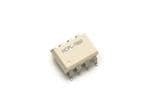
| 描述 | OPTOCOUPLER MOD SIGM-DELTA 8-DIP |
| 产品分类 | |
| 品牌 | Avago Technologies US Inc. |
| 数据手册 | http://www.avagotech.com/docs/AV02-0409EN |
| 产品图片 |
|
| 产品型号 | HCPL-7860 |
| PCN封装 | |
| rohs | 无铅 / 符合限制有害物质指令(RoHS)规范要求 |
| 产品系列 | - |
| 供应商器件封装 | 8-DIP |
| 其它名称 | 516-2269-5 |
| 包装 | 管件 |
| 安装类型 | 通孔 |
| 封装/外壳 | 8-DIP(0.300",7.62mm) |
| 工作温度 | -40°C ~ 85°C |
| 标准包装 | 50 |
| 电压-电源 | 4.5 V ~ 5.5 V |
| 电压-隔离 | 3750Vrms |
| 类型 | 三角积分调制器 |
| 输入类型 | DC |


- 商务部:美国ITC正式对集成电路等产品启动337调查
- 曝三星4nm工艺存在良率问题 高通将骁龙8 Gen1或转产台积电
- 太阳诱电将投资9.5亿元在常州建新厂生产MLCC 预计2023年完工
- 英特尔发布欧洲新工厂建设计划 深化IDM 2.0 战略
- 台积电先进制程称霸业界 有大客户加持明年业绩稳了
- 达到5530亿美元!SIA预计今年全球半导体销售额将创下新高
- 英特尔拟将自动驾驶子公司Mobileye上市 估值或超500亿美元
- 三星加码芯片和SET,合并消费电子和移动部门,撤换高东真等 CEO
- 三星电子宣布重大人事变动 还合并消费电子和移动部门
- 海关总署:前11个月进口集成电路产品价值2.52万亿元 增长14.8%


PDF Datasheet 数据手册内容提取
HCPL-7860/HCPL-786J Optically Isolated Sigma-Delta (S-D) Modulator Data Sheet Lead (Pb) Free RoHS 6 fully compliant RoHS 6 fully compliant options available; -xxxE denotes a lead-free product Description Features The HCPL-7860/HCPL-786J Optically Isolated Modulator • 12-bit Linearity and HCPL-0872 Digital Interface IC or digital filter together • 200 ns Conversion Time form an isolated programmable two-chip analog-to-digital (Pre-Trigger Mode 2 with HCPL-0872) converter. The isolated modulator allows direct measure- • 12-bit Effective Resolution with 5 µs Signal Delay ment of motor phase currents in power inverters. (14-bit with 102 µs) (with HCPL-0872) In operation, the HCPL-7860/HCPL-786J Isolated Modula- • Fast 3 µs Over-Range Detection (with HCPL-0872) tor converts a low-bandwidth analog input into a high- • ± 200 mV Input Range with Single 5 V Supply speed one-bit data stream by means of a Sigma-Delta (Σ−∆) over-sampling modulator. This modulation provides • 1% Internal Reference Voltage Matching for high noise margins and excellent immunity against • Offset Calibration (with HCPL-0872) isolation-mode transients. The modulator data and on- • -40°C to +85°C Operating Temperature Range chip sampling clock are encoded and transmitted across the isolation boundary where they are recovered and de- • 15 kV/µs Isolation Transient Immunity coded into separate high-speed clock and data channels. • Safety Approval: UL 1577, CSA and IEC/EN/DIN EN 60747-5-5 Applications • Motor Phase and Rail Current Sensing • Data Acquisition Systems • Industrial Process Control • Inverter Current Sensing • General Purpose Current Sensing and Monitoring 1 8 2 SIGMA 7 Input DELTA HCPL-0872 MCU Current MOD./ DECODE or or 3 ENCODE 6 Digital Filter DSP 4 5 HCPL-7860 NOTE: A 0.1 μF bypass capacitor must be connected between pins VDD1 and GND1 and between pins VDD2 and GND2. CAUTION: It is advised that normal static precautions be taken in handling and assembly of this component to prevent damage and/or degradation which may be induced by ESD. The components featured in this datasheet are not to be used in military or aerospace applications or environments.
Pin Description ISOLATION BOUNDARY V 1 16 GND2 DD1 VIN+ 2 15 NC VDD1 1 8 VDD2 VIN- 3 14 VDD2 SIGMA- VIN+ 2 SIGMA- 7 MCLK NC 4 DMEOLTDA./ DECODER 13 MCLK DELTA DECODE NC 5 ENCODER 12 NC MOD./ VIN- 3 ENCODE 6 MDAT NC 6 11 MDAT NC 7 10 NC GND1 4 5 GND2 SHIELD GND1 8 9 GND2 HCPL-7860 HCPL-786J Symbol Description Symbol Description VDD1 Supply voltage input (4.5 V to 5.5 V) VDD2 Supply voltage input (4.5 V to 5.5 V) VIN+ Positive input (± 200 mV recommended) MCLK Clock output (10 MHz typical) VIN- Negative input (normally connected to GND1) MDAT Serial data output GND1 Input ground GND2 Output ground Note: NC = No connection. Leave floating. Ordering Information HCPL-7860 is UL Recognized with 3750 Vrms for 1 minute per UL1577. HCPL-786J is UL Recognized with 5000 Vrms for 1 minute per UL1577. Option RoHS Non-RoHS Surface Gull Tape IEC/EN/DIN EN Part number Compliant Compliant Package Mount Wing & Reel 60747-5-5 Quantity HCPL-7860 -000E No option 300 mil X 50 per tube DIP-8 -300E #300 X X X 50 per tube -500E #500 X X X X 1000 per reel HCPL-786J -000E No option SO-16 X 45 per tube -500E #500 X X X 850 per reel To order, choose a part number from the part number column and combine with the desired option from the option column to form an order entry. Example 1: HCPL-7860-500E to order product of Gull Wing Surface Mount package in Tape and Reel packaging with IEC/EN/DIN EN 60747-5-5 Safety Approval in RoHS compliant. Example 2: HCPL-786J to order product of SO-16 package in tube packaging and non-RoHS compliant. Option datasheets are available. Contact your Avago sales representative or authorized distributor for information. Remarks: The notation ‘#XXX’ is used for existing products, while (new) products launched since 15th July 2001 and RoHS compliant option will use ‘-XXXE’. 2
Package Outline Drawings 8-pin DIP Package 9.80 ± 0.25 (0.386 ± 0.010) 7.62 ± 0.25 (0.300 ± 0.010) Device Part Number 8 7 6 5 6.35 ± 0.25 (0.250 ± 0.010) Avago A NNNN Z Test Rating Code Lead Free • YYWW UL Logo EEE P Special Program Code Pin 1 Dot 1 2 3 4 Date Code Lot ID 1.19 (0.047) MAX. 1.78 (0.070) MAX. + 0.076 5 TYP. 0.254 - 0.051 + 0.003) (0.010 - 0.002) 3.56 ± 0.13 4.70 (0.185) MAX. (0.140 ± 0.005) 0.51 (0.020) MIN. 2.92 (0.115) MIN. DIMENSIONS IN MILLIMETERS AND (INCHES). 1.080 ± 0.320 0.65 (0.025) MAX. OPTION NUMBERS 300 AND 500 NOT MARKED. (0.043 ± 0.013) NOTE: FLOATING LEAD PROTRUSION IS 0.25 mm (10 mils) MAX. 2.54 ± 0.25 (0.100 ± 0.010) 8-pin Gull Wing Surface Mount Option 300 9.80 ± 0.25 LAND PATTERN RECOMMENDATION (0.386 ± 0.010) 1.016 (0.040) Device Part Number 8 7 6 5 Avago A NNNN Z Test Rating Code Lead Free • YYWW UL Logo (06..235500 ±± 00..02150) 10.9 (0.430) EEE P Special Program Code Pin 1 Dot 1 2 3 4 Date Code Lot ID 2.0 (0.080) 1.27 (0.050) 1.780 9.65 ± 0.25 (0.070) (0.380 ± 0.010) 1.19 MAX. 7.62 ± 0.25 (0.047) (0.300 ± 0.010) MAX. + 0.076 0.254 - 0.051 3.56 ± 0.13 + 0.003) (0.140 ± 0.005) (0.010 - 0.002) 1.080 ± 0.320 0.635 ± 0.25 (0.043 ± 0.013) (0.025 ± 0.010) 12° NOM. 2.54 0.635 ± 0.130 (0.100) (0.025 ± 0.005) BSC DIMENSIONS IN MILLIMETERS (INCHES). LEAD COPLANARITY = 0.10 mm (0.004 INCHES). NOTE: FLOATING LEAD PROTRUSION IS 0.5 mm (20 mils) MAX. 3
Package Outline Drawing 16-Lead Surface Mount Package 0.457 LAND PATTERN RECOMMENDATION 1.270 (0.018) (0.050) 0.64 (0.025) 16 15 14 13 12 11 10 9 TYPE NUMBER DATE CODE AVAGO A XXXX LEAD-FREE YYWW 7.493 ± 0.254 11.63 (0.458) EEE (0.295 ± 0.010) PIN 1 DOT LOT ID 2.16 (0.085) 1 2 3 4 5 6 7 8 10.312 ± 0.254 (0.406 ± 0.10) 8.763 ± 0.254 ALL LEADS TO 9° (0.345 ± 0.010) BE COPLANAR ± 0.05 (0.002) 3.505 ± 0.127 0.457 0-8° 0.203 ± 0.076 (0.138 ± 0.005) (0.018) 0.64 (0.025) MIN. (0.008 ± 0.003) STANDOFF 10.363 ± 0.254 Dimensions in Millimeters (Inches) (0.408 ± 0.010) Floating lead protrusion is 0.25 mm (10 mils) Max. Note: Initial and continued variation in color of the white mold compound is normal and does not affect performance or reliability of the device 4
Recommended Pb-Free IR Profile Recommended reflow condition as per JEDEC Standard, J-STD-020 (latest revision). Non-Halide Flux should be used. Regulatory Information The HCPL-7860/HCPL-786J has been approved by the following organizations: IEC/EN/DIN EN 60747-5-5 Approved under: DIN EN 60747-5-5(VDE 0884-5):2011-11 UL Approval under UL 1577, component recognition program. File E55361. CSA Approval under CSA Component Acceptance Notice #5, File CA 88324. IEC/EN/DIN EN 60747-5-5 Insulation Characteristics [1] Description Symbol HCPL-7860 HCPL-786J Unit Installation classification per DIN VDE 0110/1.89, Table 1 for rated mains voltage ≤ 300 Vrms I - IV I - IV for rated mains voltage ≤ 450 Vrms I - III I - IV for rated mains voltage ≤ 600 Vrms I - III I - IV for rated mains voltage ≤ 1000 Vrms I - II I - III Climatic Classification 40/85/21 40/85/21 Pollution Degree (DIN VDE 0110/1.89) 2 2 Maximum Working Insulation Voltage VIORM 891 1414 Vpeak Input to Output Test Voltage, Method b [2] VPR 1670 2652 Vpeak VIORM x 1.875=VPR, 100% Production Test with tm=1 sec, Partial discharge < 5 pC Input to Output Test Voltage, Method a[2] VPR 1425 2262 Vpeak VIORM x 1.6=VPR, Type and Sample Test, tm=10 sec, Partial discharge < 5 pC Highest Allowable Overvoltage(Transient Overvoltage tini = 60 sec) VIOTM 6000 8000 Vpeak Safety-limiting values - maximum values allowed in the event of a failure. Case Temperature TS 175 175 °C Input Current [3] IS, INPUT 400 400 mA Output Power [3] PS, OUTPUT 600 600 mW Insulation Resistance at TS, VIO = 500 V RS >109 >109 W Notes: 1. Insulation characteristics are guaranteed only within the safety maximum ratings, which must be ensured by protective circuits within the applica- tion. Surface Mount Classifications is Class A in accordance with CECC00802. 2. Refer to IEC/EN/DIN EN 60747-5-5 Optoisolator Safety Standard section of the Avago Regulatory Guide to Isolation Circuits, AV02-2041EN for a detailed description of Method a and Method b partial discharge test profiles. 3. Refer to the following figure for dependence of PS and IS on ambient temperature. 800 P (mW) RENT - IS760000 ISS (mA) R U UT C 500 P N P, IS400 WER - 300 O P UT 200 P OUT 100 0 0 25 50 75 100 125 150 175 200 TS - CASE TEMPERATURE - oC 5
Insulation and Safety Related Specifications Option 300 - surface mount classification is Class A in accordance with CECC 00802. Parameter Symbol DIP-8 SO-16 Units Conditions Minimum External Air Gap L(101) 7.4 8.3 mm Measured from input terminals to output terminals, (Clearance) shortest distance through air. Minimum External Tracking L(102) 8.0 8.3 mm Measured from input terminals to output terminals, (Creepage) shortest distance path along body. Minimum Internal Plastic Gap 0.5 0.5 mm Through insulation distance conductor to conductor, (Internal Clearance) usually the straight line distance thickness between the emitter and detector. Tracking Resistance CTI >175 >175 V DIN IEC 112/VDE 0303 Part 1 (Comparative Tracking Index) Isolation Group IIIa IIIa Material Group (DIN VDE 0110, 1/89, Table 1) Absolute Maximum Ratings Parameter Symbol Min. Max. Units Note Storage Temperature TS -55 125 °C Ambient Operating Temperature TA -40 85 °C Supply Voltages VDD1, VDD2 0 5.5 V Steady-State Input Voltage VIN+, VIN- -2.0 VDD1 + 0.5 V 1 Two Second Transient Input Voltage -6.0 Output Voltages MCLK, MDAT -0.5 VDD2 + 0.5 V Lead Solder Temperature 260°C for 10 sec., 1.6 mm below seating plane Solder Reflow Temperature Profile See Maximum Solder Reflow Thermal Profile section Recommended Operating Conditions Parameter Symbol Min. Max. Units Note Ambient Operating Temperature TA -40 +85 °C Supply Voltages VDD1, VDD2 4.5 5.5 V Input Voltage VIN+, VIN- -200 +200 mV 1 Electrical Specifications (DC) Unless otherwise noted, all specifications are at VIN+ = 0 V and VIN- = 0 V, all Typical specifications are at TA = 25°C and VDD1 = VDD2 = 5 V, and all Minimum and Maximum specifications apply over the following ranges: TA = -40°C to +85°C, VDD1 = 4.5 to 5.5 V and VDD2 = 4.5 to 5.5 V. Parameter Symbol Min. Typ. Max. Units Conditions Fig. Note Average Input Bias Current IIN -0.8 µA 1 3 Average Input Resistance RIN 450 k W 3 Input DC Common-Mode CMRRIN 60 dB 4 Rejection Ratio Output Logic High Voltage VOH 3.9 4.9 V IOUT = -100 µA Output Logic Low Voltage VOL 0.1 0.6 V IOUT = 1.6 mA Output Short Circuit Current |IOSC| 30 mA VOUT = VDD2 5 or GND2 Input Supply Current IDD1 10 15 mA VIN+ = -350 mV 2 Output Supply Current IDD2 10 15 mA to +350 mV 3 Output Clock Frequency fCLK 8.2 10 13.2 MHz 4 Data Hold Time tHDDAT 15 ns 6 6
Electrical Specifications (Tested with HCPL-0872 or Sinc3 Filter) Unless otherwise noted, all specifications are at VIN+ = -200 mV to +200 mV and VIN- = 0 V; all Typical specifications are at TA = 25°C and VDD1 = VDD2 = 5 V, and all Minimum and Maximum specifications apply over the following ranges: TA = -40°C to +85°C, VDD1 = 4.5 to 5.5 V and VDD2 = 4.5 to 5.5 V. STATIC CHARACTERISTICS Parameter Symbol Min. Typ. Max. Units Conditions Fig. Note Resolution 15 bits 7 Integral Nonlinearity INL 3 30 LSB 5 8 0.01 0.14 % 6 8 Differential Nonlinearity DNL 1 LSB 9 Uncalibrated Input Offset VOS -3 0 3 mV VIN+ = 0 V 7 Offset Drift vs. Temperature dVOS/dTA 2 10 µV/°C VIN+ = 0 V 7 10 Offset drift vs. VDD1 dVOS/dVDD1 0.12 mV/V VIN+ = 0 V 7 Internal Reference Voltage VREF 320 mV 8 Absolute Reference Voltage Tolerance -4 4 % 8 2 Reference Voltage HCPL-7860 -1 1 % TA = 25°C. 8 2 Matching HCPL-786J -2 2 % VREF Drift vs. Temperature dVREF/dTA 60 ppm/°C. 8 VREF Drift vs. VDD1 dVREF/dVDD1 0.2 % 8 Full Scale Input Range -VREF +VREF mV 11 Recommended Input Voltage Range -200 +200 mV DYNAMIC CHARACTERISTICS (Digital Interface IC HCPL-0872 is set to Conversion Mode 3.) Parameter Symbol Min. Typ. Max. Units Conditions Fig. Note Signal-to-Noise Ratio SNR 62 73 dB VIN+ = 35 Hz, 9,10 400 mVpk-pk Total Harmonic Distortion THD -67 dB (141 mVrms) Signal-to-(Noise + Distortion) SND 66 dB sine wave. Effective Number of Bits ENOB 10 12 bits 11 12 Conversion Time tC2 0.2 0.8 µs Pre-Trigger Mode 2 1,12 13 tC1 19 23 µs Pre-Trigger Mode 1 1,12 13 tC0 39 47 µs Pre-Trigger Mode 0 1,12 Signal Delay tDSIG 19 23 µs 13 14 Over-Range Detect Time tOVR1 2.0 3.0 4.2 µs VIN+ = 0 to 400mV 14 15 step waveform Threshold Detect Time (default tTHR1 10 µs 16 configuration) Signal Bandwidth BW 18 22 kHz 15 17 Isolation Transient Immunity CMR 15 20 kV/µs VISO = 1 kV 18 7
Package Characteristics Parameter Symbol Device Min. Typ. Max. Units Conditions Note Input-Output Momentary VISO HCPL-7860 3750 Vrms RH ≤ 50%, t = 1 min; 19, 20 Withstand Voltage* HCPL-786J 5000 TA = 25°C Input-Output Resistance RI-O 1012 1013 W VI-O = 500 Vdc 20 1011 TA = 100°C Input-Output Capacitance CI-O 1.4 pF f = 1 MHz 20 Input IC Junction-to-Case qjci 96 °C/W Thermocouple located at center Thermal Resistance underside of package Output IC Junction-to-Case qjco 114 °C/W Thermal Resistance *The Input-Output Momentary Withstand Voltage is a dielectric voltage rating that should not be interpreted as an input-output continuous voltage rating. For the continuous voltage rating refer to the IEC/EN/DIN EN 60747-5-5 Insulation Characteristics Table (if applicable), your equipment level safety specification, or Avago Technologies Application Note 1074, “Optocoupler Input-Output Endurance Voltage.” Notes: 1. If VIN- (pin 3) is brought above VDD1 - 2 V with respect to GND1 an internal optical-coupling test mode may be activated. This test mode is not intended for customer use. 2. All units within each HCPL-7860 standard packaging increment (either 50 per tube or 1000 per reel) have a Reference Voltage Matching of ± 1%. An Absolute Reference Voltage Tolerance of ± 4% is guaranteed between standard packaging increments. 3. Because of the switched-capacitor nature of the isolated modulator, time averaged values are shown. 4. CMRRIN is defined as the ratio of the gain for differential inputs applied between VIN+ and VIN- to the gain for common-mode inputs applied to both VIN+ and VIN- with respect to input ground GND1. 5. Short-circuit current is the amount of output current generated when either output is shorted to VDD2 or GND2. Use under these conditions is not recommended. 6. Data hold time is amount of time that the data output MDAT will stay stable following the rising edge of output clock MCLK. 7. Resolution is defined as the total number of output bits. The useable accuracy of any A/D converter is a function of its linearity and signal-to-noise ratio, rather than how many total bits it has. 8. Integral nonlinearity is defined as one-half the peak-to-peak deviation of the best-fit line through the transfer curve for VIN+ = -200 mV to +200 mV, expressed either as the number of LSBs or as a percent of measured input range (400 mV). 9. Differential nonlinearity is defined as the deviation of the actual difference from the ideal difference between midpoints of successive output codes, expressed in LSBs. 10. Data sheet value is the average magnitude of the difference in offset voltage from TA =25°C to TA= 85°C, expressed in microvolts per °C. Three standard deviation from typical value is less than 6 µV/°C. 11. Beyond the full-scale input range the output is either all zeroes or all ones. 12. The effective number of bits (or effective resolution) is defined by the equation ENOB = (SNR-1.76)/6.02 and represents the resolution of an ideal, quantization-noise limited A/D converter with the same SNR. 13. Conversion time is defined as the time from when the convert start signal CS is brought low to when SDAT goes high, indicating that output data is ready to be clocked out. This can be as small as a few cycles of the isolated modulator clock and is determined by the frequency of the isolated modulator clock and the selected Conversion and Pre-Trigger modes. For determining the true signal delay characteristics of the A/D converter for closed-loop phase margin calculations, the signal delay specification should be used. 14. Signal delay is defined as the effective delay of the input signal through the Isolated A/D converter. It can be measured by applying a -200 mV to ± 200 mV step at the input of modulator and adjusting the relative delay of the convert start signal CS so that the output of the converter is at mid scale. The signal delay is the elapsed time from when the step signal is applied at the input to when output data is ready at the end of the conver- sion cycle. The signal delay is the most important specification for determining the true signal delay characteristics of the A/D converter and should be used for determining phase margins in closed-loop applications. The signal delay is determined by the frequency of the modulator clock and which Conversion Mode is selected, and is independent of the selected Pre-Trigger Mode and, therefore, conversion time. 15. The minimum and maximum overrange detection time is determined by the frequency of the channel 1 isolated modulator clock. 16. The minimum and maximum threshold detection time is determined by the user-defined configuration of the adjustable threshold detection circuit and the frequency of the channel 1 isolated modulator clock. See the Applications Information section for further detail. The specified times apply for the default configuration. 17. The signal bandwidth is the frequency at which the magnitude of the output signal has decreased 3 dB below its low-frequency value. The signal bandwidth is determined by the frequency of the modulator clock and the selected Conversion Mode. 18. The isolation transient immunity (also known as Common-Mode Rejection) specifies the minimum rate-of-rise of an isolation-mode signal applied across the isolation boundary beyond which the modulator clock or data signals are corrupted. 19. In accordance with UL1577, for devices with minimum VISO specified at 3750 Vrms(HCPL-7860) or 5000 Vmrs (HCPL-786J) , each isolated modulator (optocoupler) is proof-tested by applying an insulation test voltage greater than 4500 Vrms (HCPL-7860) or 6000 Vrms (HCPl-786J) for one second. This test is performed before the Method b, 100% production test for partial discharge shown in IEC/EN/DIN EN 60747-5-5 Insulation Characteristics Table. 20. This is a two-terminal measurement: pins 1-4 are shorted together and pins 5-8 are shorted together. 8
1 10.5 0 -40 °C 25 °C -1 10.0 85 °C -2 -3 9.5 mA mA I - IN --45 - DD1 9.0 I -6 -7 8.5 -8 -9 8.0 -6 -4 -2 0 2 4 6 -400 -200 0 200 400 VIN - V VIN - mV Figure 1. IIN vs. VIN. Figure 2. IDD1 vs. VIN. 9.4 10.0 V = 4.5 V DD1 9.2 9.8 VDD1 = 5.0 V V = 5.5 V 9.0 MHz 9.6 DD1 Y - A 8.8 NC 9.4 m E I - DD2 8.6 K FREQU 9.2 8.4 OC 9.0 L -40 °C C 8.2 25 °C 8.8 85 °C 8.0 8.6 -400 -200 0 200 400 -40 -15 10 35 60 85 V - mV TEMPERATURE - °C IN Figure 3. IDD2 vs. VIN. Figure 4. Clock Frequency vs. Temperature. 7 0.02 6 VVVDDDDDD111 === 455...505 VVV 0.018 VVVDDDDDD111 === 455...505 VVV 0.016 5 B 0.014 LS % NL- NL- 0.012 I 4 I 0.01 3 0.008 2 0.006 -40 -15 10 35 60 85 -40 -15 10 35 60 85 TEMPERATURE - °C TEMPERATURE - °C Figure 5. INL (Bits) vs. Temperature Figure 6. INL (%) vs. Temperature 9
150 0.8 V = 4.5 V DD1 100 0.6 VDD1 = 5.0 V V = 5.5 V DD1 V µ 50 % 0.4 FFSET CHANGE - -500 V CHANGE - REF 0.02 O V = 4.5 V DD1 -100 VDD1 = 5.0 V -0.2 V = 5.5 V DD1 -150 -0.4 -40 -15 10 35 60 85 -40 -15 10 35 60 85 TEMPERATURE - °C TEMPERATURE - °C Figure 7. Offset Change vs. Temperature Figure 8. VREF Change vs. Temperature 68 80 67 75 66 70 65 65 NR NR S64 S60 63 55 V = 4.5 V DD1 62 VDD1 = 5.0 V 50 V = 5.5 V DD1 61 45 -40 -15 10 35 60 85 1 2 3 4 5 TEMPERATURE - °C CONVERSION MODE # Figure 9. SNR vs. Temperature Figure 10. SNR vs. Conversion Mode. 14 200 180 PRE-TRIGGER MODE 0 BITS) 13 160 PPRREE--TTRRIIGGGGEERR MMOODDEE 21 OLUTION (# 1112 TIME - µs 111042000 E RES 10 SION 80 EFFECTIV 9 CONVER 6400 20 8 0 1 2 3 4 5 1 2 3 4 5 CONVERSION MODE # CONVERSION MODE # Figure 11. Effective Resolution vs. Conversion Mode. Figure 12. Conversion Time vs. Conversion Mode. 10
100 90 80 VIN+ (200 mV/DIV.) 70 Y - µs 60 OVR1 (200 mV/DIV.) A EL 50 THR1 D AL 40 (2 V/DIV.) N G SI 30 20 10 0 1 2 3 4 5 2 µs/DIV. CONVERSION MODE # Figure 13. Signal Delay vs. Conversion Mode. Figure 14. Over-Range and Threshold Detect Times. 100 Application Information 90 Digital Current Sensing Hz 80 As shown in Figure 16, using the Isolated 2-chip A/D con- DTH - k 6700 verter to sense current can be as simple as connecting a DWI 50 N current-sensing resistor, or shunt, to the input and reading BA 40 L output data through the 3-wire serial output interface. NA 30 G By choosing the appropriate shunt resistance, any range SI 20 of current can be monitored, from less than 1 A to more 10 than 100 A. 0 1 2 3 4 5 Even better performance can be achieved by fully utilizing CONVERSION MODE # the more advanced features of the Isolated A/D converter, Figure 15. Signal Bandwidth vs. Conversion Mode. such as the pre-trigger circuit, which can reduce conver- sion time to less than 1 µs, the fast over-range detector for quickly detecting short circuits, different conversion modes giving various resolution/speed trade-offs, offset calibration mode to eliminate initial offset from measure- ments, and an adjustable threshold detector for detecting non-short circuit overload conditions. NON-ISOLATED + 5 V ISOLATED CCLK V DD + 5 V CLAT CHAN + V V CDAT SCLK INPUT DD1 DD2 3-WIRE CURRENT RSHUNT VIN+ MCLK MCLK1 SDAT SERIAL 0.02 C1 V MDAT MDAT1 CS INTERFACE 0.1 µF IN- GND1 GND2 0.C1 2µF MCLK2 THR1 + C3 MDAT2 OVR1 10 µF HCPL-7860/ GND RESET HCPL-786J HCPL-0872 Figure 16. Typical Application Circuit. 11
Product Description The HCPL-7860/HCPL-786J Isolated Modulator (optocou- five conversion modes, which have different combina- pler) uses sigma-delta modulation to convert an analog tions of speed and resolution to achieve the desired level input signal into a high-speed (10 MHz) single-bit digital of performance. Other functions of the HCPL-0872 Digital data stream; the time average of the modulator’s single- Interface IC include a Phase Locked Loop based pre-trigger bit data is directly proportional to the input signal. The circuit that can either give more precise control of the ef- isolated modulator’s other main function is to provide fective sampling time or reduce conversion time to less galvanic isolation between the analog input and the digital than 1 µs, a fast over-range detection circuit that rapidly output. An internal voltage reference determines the full- indicates when the magnitude of the input signal is be- scale analog input range of the modulator (approximately yond full-scale, an adjustable threshold detection circuit ± 320 mV); an input range of ± 200 mV is recommended that indicates when the magnitude of the input signal is to achieve optimal performance. above a user adjustable threshold level, an offset calibra- tion circuit, and a second multiplexed input that allows a HCPL-7860/HCPL-786J can be used together with HCPL- second Isolated Modulator to be used with a single Digital 0872, Digital Interface IC or a digital filter. The primary Interface IC. functions of the HCPL-0872 Digital Interface IC are to de- rive a multi-bit output signal by averaging the single-bit The digital output format of the Isolated A/D Converter is modulator data, as well as to provide a direct microcon- 15 bits of unsigned binary data. The input full-scale range troller interface. The effective resolution of the multi-bit and code assignment is shown in Table 1 below. Although output signal is a function of the length of time (measured the output contains 15 bits of data, the effective resolution in modulator clock cycles) over which the average is taken; is lower and is determined by selected conversion mode as averaging over longer periods of time results in higher shown in Table 2 below. resolution. The Digital Interface IC can be configured for Table 1. Input Full-Scale Range and Code Assignment. Analog Input Voltage Input Digital Output Full Scale Range 640 mV 32768 LSBs Minimum Step Size 20 µV 1 LSB +Full Scale +320 mV 111111111111111 Zero 0 mV 100000000000000 -Full Scale -320 mV 000000000000000 Table 2. Isolated A/D Converter Typical Performance Characteristics. Conversion Time (µs) Signal-to- Effective Pre-Trigger Mode Noise Ratio Resolution Signal Signal Band- Conversion Mode (dB) (bits) 0 1 2 Delay(µs) width (kHz) 1 83 13.5 205 102 102 3.4 2 79 12.8 103 51 51 6.9 3 73 11.9 39 19 0.2 19 22 4 66 10.7 20 10 10 45 5 53 8.5 10 5 5 90 Notes: Bold italic type indicates Default values. 12
Power Supplies and Bypassing The recommended application circuit is shown in Figure An inexpensive 78L05 three-terminal regulator can also be 17. A floating power supply (which in many applications used to reduce the floating supply voltage to 5 V. To help could be the same supply that is used to drive the high- attenuate high-frequency power supply noise or ripple, a side power transistor) is regulated to 5 V using a simple resistor or inductor can be used in series with the input of zener diode (D1); the value of resistor R1 should be chosen the regulator to form a low-pass filter with the regulator’s to supply sufficient current from the existing floating sup- input bypass capacitor. ply. The voltage from the current sensing resistor or shunt As shown in Figure 17, 0.1 µF bypass capacitors (C1 and (Rsense) is applied to the input of the HCPL-7860/HCPL- C3) should be located as close as possible to the input 786J (U2) through an RC anti-aliasing filter (R2 and C2). And and output power-supply pins of the isolated modulator finally, the output clock and data of the isolated modulator (U2). The bypass capacitors are required because of the are connected to the digital interface IC. Although the high-speed digital nature of the signals inside the isolated application circuit is relatively simple, a few recommenda- modulator. A 0.01 µF bypass capacitor (C2) is also recom- tions should be followed to ensure optimal performance. mended at the input due to the switched-capacitor nature The power supply for the isolated modulator is most of the input circuit. The input bypass capacitor also forms often obtained from the same supply used to power the part of the anti-aliasing filter, which is recommended to power transistor gate drive circuit. If a dedicated supply is prevent high-frequency noise from aliasing down to lower required, in many cases it is possible to add an additional frequencies and interfering with the input signal. winding on an existing transformer. Otherwise, some sort of simple isolated supply can be used, such as a line pow- ered transformer or a high-frequency DC-DC converter. FLOATING POSITIVE SUPPLY + 5 V HV+ GATE DRIVE CIRCUIT R1 CCLK V DD 5.D11 V 0.1C 1µF CLAT CHAN V V CDAT SCLK R2 39 Ω DD1 DD2 V MCLK MCLK1 SDAT IN+ MOTOR VIN- MDAT MDAT1 CS + - GND1 GND2 C3 MCLK2 THR1 RSENSE 0.0C12 µF 0.1 µF MDAT2 OVR1 HCPL-7860/ HCPL-786J GND RESET TO HCPL-0872 CONTROL CIRCUIT HV- Figure 17. Recommended Application Circuit. 13
PC Board Layout The design of the printed circuit board (PCB) should follow The maximum average power dissipation in the shunt good layout practices, such as keeping bypass capacitors can also be easily calculated by multiplying the shunt close to the supply pins, keeping output signals away resistance times the square of the maximum RMS current, from input signals, the use of ground and power planes, which is about 1 W in the previous example. etc. In addition, the layout of the PCB can also affect the If the power dissipation in the shunt is too high, the resis- isolation transient immunity (CMR) of the isolated modu- tance of the shunt can be decreased below the maximum lator, due primarily to stray capacitive coupling between value to decrease power dissipation. The minimum value the input and the output circuits. To obtain optimal CMR of the shunt is limited by precision and accuracy require- performance, the layout of the PC board should minimize ments of the design. As the shunt value is reduced, the any stray coupling by maintaining the maximum possible output voltage across the shunt is also reduced, which distance between the input and output sides of the circuit means that the offset and noise, which are fixed, become and ensuring that any ground or power plane on the PC a larger percentage of the signal amplitude. The selected board does not pass directly below or extend much wider value of the shunt will fall somewhere between the mini- than the body of the isolated modulator. mum and maximum values, depending on the particular requirements of a specific design. Shunt Resistors When sensing currents large enough to cause significant The current-sensing shunt resistor should have low re- heating of the shunt, the temperature coefficient (tempco) sistance (to minimize power dissipation), low inductance of the shunt can introduce nonlinearity due to the sig- (to minimize di/dt induced voltage spikes which could nal dependent temperature rise of the shunt. The effect adversely affect operation), and reasonable tolerance (to increases as the shunt-to-ambient thermal resistance maintain overall circuit accuracy). Choosing a particular increases. This effect can be minimized either by reducing value for the shunt is usually a compromise between the thermal resistance of the shunt or by using a shunt minimizing power dissipation and maximizing accuracy. with a lower tempco. Lowering the thermal resistance can Smaller shunt resistances decrease power dissipation, be accomplished by repositioning the shunt on the PC while larger shunt resistances can improve circuit accuracy board, by using larger PC board traces to carry away more by utilizing the full input range of the isolated modulator. heat, or by using a heat sink. The first step in selecting a shunt is determining how much current the shunt will be sensing. The graph in Figure 18 shows the RMS current in each phase of a three-phase 40 R 440 induction motor as a function of average motor output WE 35 380 O 220 power (in horsepower, hp) and motor drive supply volt- EP 30 120 S age. The maximum value of the shunt is determined by the OR H 25 current being measured and the maximum recommended R - WE 20 input voltage of the isolated modulator. The maximum O P shunt resistance can be calculated by taking the maximum UT 15 P recommended input voltage and dividing by the peak cur- OUT 10 rent that the shunt should see during normal operation. OR T 5 O For example, if a motor will have a maximum RMS current M 0 of 10 A and can experience up to 50% overloads during 0 5 10 15 20 25 30 35 normal operation, then the peak current is 21.1 A (= 10 x MOTOR PHASE CURRENT - A (rms) 1.414 x 1.5). Assuming a maximum input voltage of 200 Figure 18. Motor Output Horsepower vs. Motor Phase Current and Supply mV, the maximum value of shunt resistance in this case Voltage. would be about 10 mW. 14
For a two-terminal shunt, as the value of shunt resistance the increased power dissipation at higher currents. decreases, the resistance of the leads becomes a signifi- When laying out a PC board for the shunts, a couple of cant percentage of the total shunt resistance. This has two points should be kept in mind. The Kelvin connections primary effects on shunt accuracy. First, the effective resis- to the shunt should be brought together under the body tance of the shunt can become dependent on factors such of the shunt and then run very close to each other to the as how long the leads are, how they are bent, how far they input of the isolated modulator; this minimizes the loop are inserted into the board, and how far solder wicks up area of the connection and reduces the possibility of stray the lead during assembly (these issues will be discussed in magnetic fields from interfering with the measured signal. more detail shortly). Second, the leads are typically made If the shunt is not located on the same PC board as the from a material such as copper, which has a much higher isolated modulator circuit, a tightly twisted pair of wires tempco than the material from which the resistive element can accomplish the same thing. itself is made, resulting in a higher tempco for the shunt overall. Both of these effects are eliminated when a four- Also, multiple layers of the PC board can be used to in- terminal shunt is used. A four-terminal shunt has two ad- crease current carrying capacity. Numerous plated-through ditional terminals that are Kelvin-connected directly across vias should surround each non-Kelvin terminal of the shunt the resistive element itself; these two terminals are used to help distribute the current between the layers of the PC to monitor the voltage across the resistive element while board. The PC board should use 2 or 4 oz. copper for the the other two terminals are used to carry the load current. layers, resulting in a current carrying capacity in excess of Because of the Kelvin connection, any voltage drops across 20 A. Making the current carrying traces on the PC board the leads carrying the load current should have no impact fairly large can also improve the shunt’s power dissipa- on the measured voltage. tion capability by acting as a heat sink. Liberal use of vias where the load current enters and exits the PC board is Several four-terminal shunts from Isotek (Isabellenhütte) also recommended. suitable for sensing currents in motor drives up to 71 Arms (71 hp or 53 kW) are shown in Table 3; the maximum current and motor power range for each of the PBV series shunts are indicated. For shunt resistances from 50 mW down to 10 mW, the maximum current is limited by the input voltage range of the isolated modulator. For the 5 mW and 2 mW shunts, a heat sink may be required due to Table 3. Isotek (Isabellenhütte) Four-Terminal Shunt Summary. Maximum RMS Cur- Motor Power Range Shunt Resistor Shunt Resistance Tol. rent 120 VAC - 440 VAC Part Number mW % A hp kW PBV-R050-0.5 50 0.5 3 0.8 - 3 0.6 - 2 PBV-R020-0.5 20 0.5 7 2 - 7 0.6 - 2 PBV-R010-0.5 10 0.5 14 4 - 14 3 - 10 PBV-R005-0.5 5 0.5 25 [28] 7 - 25 [8 - 28] 5 - 19 [6 - 21] PBV-R002-0.5 2 0.5 39 [71] 11 - 39 [19 - 71] 8 - 29 [14 - 53] Note: Values in brackets are with a heatsink for the shunt. 15
Shunt Connections The recommended method for connecting the isolated In some applications, however, supply currents flowing modulator to the shunt resistor is shown in Figure 17. VIN+ through the power-supply return path may cause offset (pin 2 of the HPCL-7860/HCPL-786J) is connected to the or noise problems. In this case, better performance may positive terminal of the shunt resistor, while VIN- (pin 3) is be obtained by connecting VIN+ and VIN- directly across shorted to GND1 with the power-supply return path func- the shunt resistor with two conductors, and connecting tioning as the sense line to the negative terminal of the GND1 to the shunt resistor with a third conductor for the current shunt. This allows a single pair of wires or PC board power-supply return path, as shown in Figure 19. When traces to connect the isolated modulator circuit to the connected this way, both input pins should be bypassed. shunt resistor. By referencing the input circuit to the nega- To minimize electromagnetic interference of the sense sig- tive side of the sense resistor, any load current induced nal, all of the conductors (whether two or three are used) noise transients on the shunt are seen as a common-mode connecting the isolated modulator to the sense resistor signal and will not interfere with the current-sense signal. should be either twisted pair wire or closely spaced traces This is important because the large load currents flowing on a PC board. through the motor drive, along with the parasitic induc- The 39 W resistor in series with the input lead (R2) forms tances inherent in the wiring of the circuit, can generate a lowpass anti-aliasing filter with the 0.01 µF input bypass both noise spikes and offsets that are relatively large com- capacitor (C2) with a 400 kHz bandwidth. The resistor per- pared to the small voltages that are being measured across forms another important function as well; it dampens any the current shunt. ringing which might be present in the circuit formed by If the same power supply is used both for the gate drive cir- the shunt, the input bypass capacitor, and the inductance cuit and for the current sensing circuit, it is very important of wires or traces connecting the two. Undamped ringing that the connection from GND1 of the isolated modulator of the input circuit near the input sampling frequency can to the sense resistor be the only return path for supply cur- alias into the baseband producing what might appear to rent to the gate drive power supply in order to eliminate be noise at the output of the device. potential ground loop problems. The only direct connec- tion between the isolated modulator circuit and the gate drive circuit should be the positive power supply line. FLOATING POSITIVE SUPPLY HV+ GATE DRIVE CIRCUIT R1 D1 C1 5.1 V 0.1 µF R2a 39 Ω V V DD1 DD2 R2b 39 Ω V MCLK IN+ MOTOR VIN- MDAT + - GND1 GND2 R C2a C2b SENSE 0.01 µF 0.01 µF HCPL-7860/ HCPL-786J HV- Figure 19. Schematic for Three Conductor Shunt Connection. 16
Voltage Sensing The HCPL-7860/HCPL-786J Isolated Modulator can also be used to isolate signals with amplitudes larger than its recommended input range with the use of a resistive volt- age divider at its input. The only restrictions are that the impedance of the divider be relatively small (less than 1 kW) so that the input resistance (280 kW) and input bias current (1 µA) do not affect the accuracy of the measure- ment. An input bypass capacitor is still required, although the 39 W series damping resistor is not (the resistance of the voltage divider provides the same function). The low- pass filter formed by the divider resistance and the input bypass capacitor may limit the achievable bandwidth. To obtain higher bandwidth, the input bypass capacitor (C2) can be reduced, but it should not be reduced much below 1000 pF to maintain adequate input bypassing of the iso- lated modulator. For product information and a complete list of distributors, please go to our web site: www.avagotech.com Avago, Avago Technologies, and the A logo are trademarks of Avago Technologies in the United States and other countries. Data subject to change. Copyright © 2005-2015 Avago Technologies. All rights reserved. Obsoletes 5989-2166EN AV02-0409EN - March 6, 2015
Mouser Electronics Authorized Distributor Click to View Pricing, Inventory, Delivery & Lifecycle Information: B roadcom Limited: HCPL-7860 HCPL-786J