ICGOO在线商城 > 集成电路(IC) > 数据采集 - 模拟前端(AFE) > AD73322LARUZ
 Datasheet下载
- 型号: AD73322LARUZ
- 制造商: Analog
- 库位|库存: xxxx|xxxx
- 要求:
| 数量阶梯 | 香港交货 | 国内含税 |
| +xxxx | $xxxx | ¥xxxx |
查看当月历史价格
查看今年历史价格
AD73322LARUZ产品简介:
ICGOO电子元器件商城为您提供AD73322LARUZ由Analog设计生产,在icgoo商城现货销售,并且可以通过原厂、代理商等渠道进行代购。 AD73322LARUZ价格参考。AnalogAD73322LARUZ封装/规格:数据采集 - 模拟前端(AFE), 2 Channel AFE 16 Bit 73mW 28-TSSOP。您可以下载AD73322LARUZ参考资料、Datasheet数据手册功能说明书,资料中有AD73322LARUZ 详细功能的应用电路图电压和使用方法及教程。
AD73322LARUZ 是由 Analog Devices Inc.(ADI)生产的一款数据采集系统中的模拟前端(AFE)芯片。它主要应用于需要高精度、低功耗和多通道数据采集的场景,以下是其典型应用场景:

1. 工业自动化与控制
   - 该芯片适用于工业自动化设备中对传感器信号的采集和处理,例如温度、压力、振动等信号的监测。其多通道特性可以同时采集多个传感器的数据,满足复杂工业系统的监控需求。

2. 医疗设备
   - 在医疗领域,AD73322LARUZ 可用于心电图(ECG)、脑电图(EEG)和其他生物电势测量设备中。其高精度和低噪声性能能够准确捕捉微弱的生理信号,确保诊断结果的可靠性。

3. 能源管理
   - 该芯片可用于智能电网、电力监测和电池管理系统(BMS)。它可以精确地采集电压、电流等参数,并提供实时反馈,以优化能源使用效率。

4. 环境监测
   - 在环境监测系统中,AD73322LARUZ 能够采集空气污染、水质分析或气象站中的各种模拟信号,如气体浓度、湿度、光照强度等,为环境保护提供数据支持。

5. 测试与测量设备
   - 它广泛应用于示波器、信号发生器和其他精密测量仪器中,帮助实现对电子信号的高效采集和分析。

6. 汽车电子
   - 在汽车行业中,该芯片可用于发动机控制单元(ECU)、胎压监测系统(TPMS)以及车辆稳定性控制系统中,提供高精度的数据采集功能。

总之,AD73322LARUZ 凭借其出色的性能和灵活性,适合需要高性能数据采集的多种应用场合,尤其是在对精度、可靠性和低功耗有较高要求的领域中表现优异。
| 参数 | 数值 |
| ADC数量 | 2 |
| 产品目录 | 集成电路 (IC)半导体 |
| DAC数量 | 2 |
| 描述 | IC PROCESSOR FRONTEND DL 28TSSOP接口—CODEC Dual-Ch 3V Front-End Processor |
| 产品分类 | 数据采集 - 模拟前端 (AFE)集成电路 - IC |
| 品牌 | Analog Devices |
| 产品手册 | |
| 产品图片 |
|
| rohs | 符合RoHS无铅 / 符合限制有害物质指令(RoHS)规范要求 |
| 产品系列 | 接口 IC,接口—CODEC,Analog Devices AD73322LARUZ- |
| 数据手册 | |
| 产品型号 | AD73322LARUZ |
| THD+噪声 | - 86 dB ADC/- 89 dB DAC |
| 产品种类 | 接口—CODEC |
| 位数 | 16 |
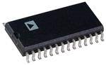
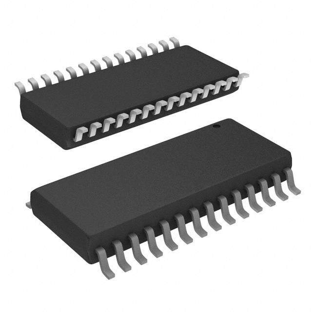
| 供应商器件封装 | 28-TSSOP |
| 信噪比 | 78 dB ADC/78 dB DAC |
| 分辨率 | 16 bit |
| 功率(W) | 73mW |
| 包装 | 管件 |
| 商标 | Analog Devices |
| 安装风格 | SMD/SMT |
| 封装 | Tube |
| 封装/外壳 | 28-TSSOP(0.173",4.40mm 宽) |
| 封装/箱体 | TSSOP-28 |
| 工厂包装数量 | 50 |
| 接口类型 | Serial |
| 最大工作温度 | + 85 C |
| 最小工作温度 | - 40 C |
| 标准包装 | 50 |
| 电压-电源,数字 | 2.7 V ~ 5.5 V |
| 电压-电源,模拟 | 2.7 V ~ 5.5 V |
| 电源电流 | 31 mA |
| 类型 | Audio CODEC, Voice Band |
| 系列 | AD73322L |
| 转换速率 | 64 kHz |
| 通道数 | 4 |


PDF Datasheet 数据手册内容提取
Low Cost, Low Power CMOS General-Purpose Dual Analog Front End AD73322L FEATURES FUNCTIONAL BLOCK DIAGRAM Two 16-bit A/D converters AVDD1 AVDD2 DVDD Two 16-bit D/A converters AD73322L Programmable input/output sample rates VFBP1 78 dB ADC SNR VINP1 ADC CHANNEL 1 SDI VINN1 SDIFS 78 dB DAC SNR VFBN1 64 kHz maximum sample rate VOUTP1 DAC CHANNEL 1 SCLK −90 dB crosstalk VOUTN1 Low group delay (25 µs typ per ADC channel, 50 µs typ per REFOUT SE DAC channel) REFERENCE SPORT REFCAP RESET Programmable input/output gain VFBP2 Flexible serial port allows up to 4 dual codecs to be VINP2 ADC CHANNEL 2 MCLK VINN2 connected in cascade, giving 8 I/O channels VFBN2 Single-supply operation (2.7 V to 3.3 V) VOUTP2 SDOFS 50 mW typ power consumption at 3.0 V VOUTN2 DAC CHANNEL 2 SDO Temperature range: −40°C to +105°C O28n--lcehaidp S rOefIeCr,e TnScSeO P, and 44-lead LQFP packages AGND1 AGND2 DGND 00691-001 APPLICATIONS Figure 1. General-purpose analog I/O Speech processing Cordless and personal communications Telephony Active control of sound and vibration Data communications Wireless local loop GENERAL DESCRIPTION The AD73322L is a dual front-end processor for general- The A/D and D/A conversion channels feature programmable purpose applications, including speech and telephony. It input/output gains with ranges of 38 dB and 21 dB, respectively. features two 16-bit A/D conversion channels and two 16-bit An on-chip reference voltage allows single-supply operation. D/A conversion channels. Each channel provides 78 dB signal- The sampling rate of the codecs is programmable with four to-noise ratio over a voice-band signal bandwidth. It also separate settings offering 64 kHz, 32 kHz, 16 kHz, and 8 kHz features an input-to-output gain network in both the analog sampling rates (from a master clock of 16.384 MHz). and digital domains. This is featured on both codecs and can be used for impedance matching or scaling when interfacing to A serial port (SPORT) allows easy interfacing of single or subscriber line interface circuits (SLICs). cascaded devices to industry-standard DSP engines. The SPORT transfer rate is programmable to allow interfacing to The AD73322L is particularly suitable for a variety of appli- both fast and slow DSP engines. cations in the speech and telephony area, including low bit rate, high quality compression, speech enhancement, recognition, The AD73322L is available in 28-lead SOIC, 28-lead TSSOP, and synthesis. The low group delay characteristic of the part and 44-lead LQFP packages. makes it suitable for single or multichannel active control applications. Rev. A Information furnished by Analog Devices is believed to be accurate and reliable. However, no responsibility is assumed by Analog Devices for its use, nor for any infringements of patents or other rights of third parties that may result from its use. One Technology Way, P.O. Box 9106, Norwood, MA 02062-9106, U.S.A. Specifications subject to change without notice. No license is granted by implication or otherwise under any patent or patent rights of Analog Devices. Trademarks and Tel: 781.329.4700 www.analog.com registered trademarks are the property of their respective owners. Fax: 781.326.8703 © 2004 Analog Devices, Inc. All rights reserved.
AD73322L TABLE OF CONTENTS Specifications.....................................................................................4 Sample Rate Divider...................................................................19 Current Summary.........................................................................6 DAC Advance Register..............................................................20 Signal Ranges................................................................................7 Control Register A.....................................................................21 Timing Characteristics................................................................7 Control Register B......................................................................21 Timing Diagrams..........................................................................8 Control Register C......................................................................21 Absolute Maximum Ratings............................................................9 Control Register D.....................................................................22 ESD Caution..................................................................................9 Control Register E......................................................................22 Pin Configurations and Function Descriptions.........................10 Control Register F......................................................................22 Terminology....................................................................................12 Control Register G.....................................................................23 Abbreviations..............................................................................12 Control Register H.....................................................................23 Typical Performance Characteristics and Functional Block Operation.........................................................................................24 Diagram...........................................................................................13 Resetting the AD73322L...........................................................24 Functional Descriptions................................................................14 Power Management...................................................................24 Encoder Channels......................................................................14 Operating Modes........................................................................24 Programmable Gain Amplifier.................................................14 Program (Control) Mode..........................................................24 ADC.............................................................................................14 Data Mode...................................................................................25 Analog Sigma-Delta Modulator...............................................14 Mixed Program/Data Mode......................................................25 Decimation Filter........................................................................15 Digital Loop-Back Mode...........................................................25 ADC Coding...............................................................................15 SPORT Loop-Back Mode..........................................................25 Decoder Channel........................................................................16 Analog Loop-Back Mode..........................................................26 DAC Coding................................................................................16 Interfacing.......................................................................................27 Interpolation Filter.....................................................................16 Cascade Operation.....................................................................27 Analog Smoothing Filter and PGA..........................................16 Performance....................................................................................29 Differential Output Amplifiers.................................................16 Encoder Section..........................................................................29 Voltage Reference.......................................................................16 Encoder Group Delay................................................................30 Analog and Digital Gain Taps...................................................17 Decoder Section.........................................................................30 Digital Gain Tap..........................................................................18 On-Chip Filtering.......................................................................31 Serial Port (SPORT)...................................................................18 Decoder Group Delay................................................................31 SPORT Overview........................................................................18 Design Considerations...................................................................32 SPORT Register Maps................................................................19 Analog Inputs.............................................................................32 Master Clock Divider.................................................................19 Interfacing to an Electret Microphone....................................34 Serial Clock Rate Divider..........................................................19 Rev. A | Page 2 of 48
AD73322L Analog Output.............................................................................34 Mixed-Mode Operation.............................................................37 Differential-to-Single-Ended Output.......................................35 Interrupts.....................................................................................37 Digital Interfacing.......................................................................35 Initialization.................................................................................38 Cascade Operation......................................................................35 Running the AD73322L with ADCs or DACs in Power-Down .......................................................................................................38 Grounding and Layout...............................................................36 DAC Timing Control Example.....................................................40 DSP Programming Considerations..............................................37 Configuring an AD73322L to Operate in Data Mode...............41 DSP SPORT Configuration.......................................................37 Configuring an AD73322L to Operate in Mixed Mode............43 DSP SPORT Interrupts...............................................................37 Outline Dimensions........................................................................46 DSP Software Considerations When Interfacing to the AD73322L....................................................................................37 Ordering Guide...........................................................................47 Operating Mode..........................................................................37 REVISION HISTORY 12/04—Rev. 0 to Rev. A Updated Format..................................................................Universal Updated Outline Dimensions........................................................46 Changes to Ordering Guide...........................................................47 4/01—Revision 0: Initial Version Rev. A | Page 3 of 48
AD73322L SPECIFICATIONS AVDD = 3 V ± 10%; DVDD = 3 V ± 10%; DGND = AGND = 0 V, f = 16.384 MHz, f = 8 kHz; T = T to T , DMCLK SAMP A MIN MAX unless otherwise noted. Operating temperature range as follows: A grade, T = −40°C, T = +85°C; Y grade, T = −40°C, T = +105°C. MIN MAX MIN MAX Table 1. A and Y Versions Parameter Min Typ Max Unit Test Conditions/Comments REFERENCE REFCAP Absolute Voltage, VREFCAP 1.08 1.2 1.32 V REFCAP TC 50 ppm/°C 0.1 µF capacitor required from REFCAP to AGND2 REFOUT Typical Output Impedance 130 Ω Absolute Voltage, V 1.08 1.2 1.32 V Unloaded REFOUT Minimum Load Resistance 1 kΩ Maximum Load Capacitance 100 pF INPUT AMPLIFIER Offset ±1.0 mV Maximum Output Swing 1.578 V Max output swing = (1.578/1.2) × VREFCAP Feedback Resistance 50 kΩ f = 32 kHz C Feedback Capacitance 100 pF ANALOG GAIN TAP Gain at Maximum Setting +1 Gain at Minimum Setting −1 Gain Resolution 5 Bits Gain step size = 0.0625 Gain Accuracy ±1.0 % Output unloaded Settling Time 1.0 µs Tap gain change of −FS to +FS Delay 0.5 µs ADC SPECIFICATIONS DAC unloaded Maximum Input Range at VIN1, 2 1.578 V p-p Measured differentially −2.85 dBm Max input = (1.578/1.2) × VREFCAP Nominal Reference Level at VIN 1.0954 V p-p Measured differentially (0 dBm0) −6.02 dBm Absolute Gain PGA = 0 dB −2.0 −0.7 +0.5 dB 1.0 kHz, 0 dBm0 Gain Tracking Error ±0.1 dB 1.0 kHz, +3 dBm0 to −50 dBm0 Signal-to-Noise and Distortion Refer to Figure 9 PGA = 0 dB 70 78 dB 300 Hz to 3400 Hz; f = 8 kHz, PUIA = 0 SAMP 79 dB 300 Hz to 3400 Hz; f = 8 kHz, PUIA = 1 SAMP 77.5 dB 0 Hz to f /2; f = 8 kHz SAMP SAMP Total Harmonic Distortion PGA = 0 dB −86 −75 dB 300 Hz to 3400 Hz; f = 8 kHz SAMP Intermodulation Distortion −61 dB PGA = 0 dB Idle Channel Noise Crosstalk −72 dBm0 PGA = 0 dB ADC-to-DAC −107 dB ADC input signal level: 1.0 kHz, 0 dBm0 DAC input at idle ADC-to-ADC −92 dB ADC1 input signal level: 1.0 kHz, 0 dBm0 ADC2 input at idle; input amplifiers bypassed −93 dB Input amplifiers included in input channel DC Offset −20 0 +20 mV PGA = 0 dB Power Supply Rejection Ratio −65 dB Input signal level at AVDD and DVDD pins: 1.0 kHz, 100 mV p-p sine wave Rev. A | Page 4 of 48
AD73322L A and Y Versions Parameter Min Typ Max Unit Test Conditions/Comments Group Delay3, 4 25 µs Input Resistance at PGA1, 3, 5 20 kΩ Input amplifiers bypassed DIGITAL GAIN TAP Gain at Maximum Setting 1 Gain at Minimum Setting −1 Gain Resolution 16 Bits Tested to 5 MSB of settings Delay 25 µs Includes DAC delay Settling Time 100 µs Tap gain change from −FS to +FS; includes DAC settling time DAC SPECIFICATIONS DAC unloaded Maximum Voltage Output Swing1 Single-Ended 1.578 V p-p PGA = 6 dB −2.85 dBm Max output = (1.578/1.2) × VREFCAP Differential 3.156 V p-p PGA = 6 dB 3.17 dBm Max output = 2 × (1.578/1.2) × VREFCAP Nominal Voltage Output Swing (0 dBm0) Single-Ended 1.0954 V p-p PGA = 6 dB −6.02 dBm Differential 2.1909 V p-p PGA = 6 dB 0 dBm Output Bias Voltage 1.2 V REFOUT unloaded Absolute Gain −1.75 −0.6 +0.75 dB 1.0 kHz, 0 dBm0; unloaded Gain Tracking Error ±0.1 dB 1.0 kHz, +3 dBm0 to −50 dBm0 Signal-to-Noise and Distortion at 0 dBm0 Refer to Figure 10 PGA = 0 dB 72 78.5 dB 300 Hz to 3400 Hz; f = 8 kHz SAMP Total Harmonic Distortion at 0 dBm0 PGA = 0 dB −89 −75 dB 300 Hz to 3400 Hz; f = 8 kHz SAMP Intermodulation Distortion −77 dB PGA = 0 dB Idle Channel Noise Crosstalk −81 dBm0 PGA = 0 dB DAC-to-ADC −73 dB ADC input signal level: AGND; DAC output signal level: 1.0 kHz, 0 dBm0 Input amplifiers bypassed −74 dB Input amplifiers included in input channel DAC-to-DAC −102 dB DAC1 output signal level: AGND; DAC2 Output signal level: 1.0 kHz, 0 dBm0 Power Supply Rejection −65 dB Input signal level at AVDD and DVDD pins: 1.0 kHz, 100 mV p-p sine wave Group Delay3, 4 25 µs Interpolator bypassed 50 µs Output DC Offset1, 6 −50 +5 +60 mV Minimum Load Resistance, R1, 7 L Single-Ended3 150 Ω Differential 150 Ω Maximum Load Capacitance, C1, 7 L Single-Ended 500 pF Differential 100 pF FREQUENCY RESPONSE (ADC and DAC)8 Typical Output Frequency (Normalized to FS) 0 0 dB 0.03125 −0.1 dB Rev. A | Page 5 of 48
AD73322L A and Y Versions Parameter Min Typ Max Unit Test Conditions/Comments 0.0625 −0.25 dB 0.125 −0.6 dB 0.1875 −1.4 dB 0.25 −2.8 dB 0.3125 − 4.5 dB 0.375 −7.0 dB 0.4375 −9.5 dB > 0.5 <−12.5 dB LOGIC INPUTS VINH, Input High Voltage DVDD − 0.8 DVDD V V , Input Low Voltage 0 0.8 V INL I , Input Current −10 +10 µA IH C , Input Capacitance 10 pF IN LOGIC OUTPUT VOH, Output High Voltage DVDD − 0.4 DVDD V |IOUT| ≤100 µA V , Output Low Voltage 0 0.4 V |IOUT| ≤100 µA OL Three-State Leakage Current −10 +10 µA POWER SUPPLIES AVDD1, AVDD2 2.7 3.3 V 2.7 3.3 V DVDD I 9 See Table 2 DD 1 Test conditions: input PGA set for 0 dB gain, output PGA set for 6 dB gain, no load on analog outputs (unless otherwise noted). 2 At input to sigma-delta modulator of ADC. 3 Guaranteed by design. 4 Overall group delay is affected by the sample rate and the external digital filtering. 5 The ADC’s input impedance is inversely proportional to DMCLK and is approximated by (3/3 × 1011)/DMCLK. 6 Between VOUTP1 and VOUTN1 or between VOUTP2 and VOUTN2. 7 At VOUT output. 8 Frequency responses of ADC and DAC measured with input at audio reference level (the input level that produces an output level of −10 dBm0), with 38 dB preamplifier bypassed and input gain of 0 dB. 9 Test conditions: no load on digital inputs, analog inputs ac-coupled to ground, no load on analog outputs. CURRENT SUMMARY AVDD = DVDD = 3.3 V. These values are in mA and are typical values unless otherwise noted. Table 2. Analog Digital Total Total Conditions Current Current Current (Typ) Current (Max) SE MCLK ON Comments ADCs on only 3.4 6.3 9.7 12 1 YES REFOUT disabled DACs on only 8.8 6.5 15.3 20 1 YES REFOUT disabled ADCs and DACs on 11.6 7.0 18.6 23 1 YES REFOUT disabled ADCs and DACs and 13.8 7.0 20.8 26 1 YES REFOUT disabled Input amps on ADCs and DACs and 13.2 7.0 20.2 26 1 YES REFOUT disabled AGT on All sections on 17.2 7.0 24.2 31 1 YES REFCAP on only 0.65 0 0.67 1.25 0 NO REFOUT disabled REFCAP and REFOUT 2.56 0 2.57 4.5 0 NO On only All sections off 0 1.25 1.25 1.8 0 YES MCLK active levels equal to 0 V and DVDD All sections off 0 µA 12.5 µA 12.7 µA 40 µA 0 NO Digital inputs static and Equal to 0 V or DVDD Rev. A | Page 6 of 48
AD73322L SIGNAL RANGES Table 3. Mnemoic Description Range VREFCAP 1.2 V ± 10% VREFOUT 1.2 V ± 10% ADC Maximum input range at V 1.578 V p-p IN Nominal reference level 1.0954 V p-p DAC Maximum voltage output swing Single-Ended 1.578 V p-p Differential 3.156 V p-p Nominal voltage output swing Single-Ended 1.0954 V p-p Differential 2.1909 V p-p Output bias voltage VREFOUT TIMING CHARACTERISTICS AVDD = 3 V ± 10%; DVDD = 3 V ± 10%; AGND = DGND = 0 V; T = T to T , unless otherwise noted. A MlN MAX Table 4. Parameter Limit at TA = −40°C to +105°C Unit Description Clock Signals See Figure 2 t 61 ns min MCLK period 1 t 24.4 ns min MCLK width high 2 t 24.4 ns min MCLK width low 3 Serial Port See Figure 4 and Figure 5 t t ns min SCLK period 4 1 t 0.4 × t ns min SCLK width high 5 1 t 0.4 × t ns min SCLK width low 6 1 t 20 ns min SDI/SDIFS setup before SCLK low 7 t 0 ns min SDI/SDIFS hold after SCLK low 8 t 10 ns max SDOFS delay from SCLK high 9 t 10 ns min SDOFS hold after SCLK high 10 t 10 ns min SDO hold after SCLK high 11 t 10 ns max SDO delay from SCLK high 12 t 30 ns max SCLK delay from MCLK 13 Rev. A | Page 7 of 48
AD73322L TIMING DIAGRAMS t 1 t 2 t3 00691-002 Figure 2. MCLK Timing 100µA IOL TO OUTPUT 2.1V PIN CL 15pF 100µA IOH 00691-003 Figure 3. Load Circuit for Timing Specifications t t t 1 2 3 MCLK t 13 SCLK* t5 t6 t * SINC FLRKE ISQ UINEDNICVIYD (UMAC4LLLKY/ 4P RSHOOGWRANM HMEARBEL).E 00691-004 Figure 4. SCLK Timing SE (I) THREE- STATE SCLK (O) t 7 SDIFS (I) t 8 t 8 t 7 SDI (I) D15 D14 D1 D0 D15 t t THREE- 9 10 SDOFS (O) STATE THREE- t12 t11 SDO (O) STATE D15 D2 D1 D0 D15 D14 00691-005 Figure 5. Serial Port (SPORT) Rev. A | Page 8 of 48
AD73322L ABSOLUTE MAXIMUM RATINGS T = 25°C unless otherwise noted. A Table 5. Stresses above those listed under Absolute Maximum Ratings Parameters Ratings may cause permanent damage to the device. This is a stress AVDD, DVDD to GND −0.3 V to +4.6 V rating only; functional operation of the device at these or any AGND to DGND −0.3 V to +0.3 V other conditions above those listed in the operational sections Digital I/O Voltage to DGND −0.3 V to (DVDD + 0.3 V) of this specification is not implied. Exposure to absolute Analog I/O Voltage to AGND −0.3 V to (AVDD + 0.3 V) maximum rating conditions for extended periods may affect Operating Temperature Range device reliability. Industrial (A Version) −40°C to +85°C Extended (Y Version) −40°C to +105°C Storage Temperature Range −65°C to +150°C Maximum Junction Temperature 150°C SOIC, θ Thermal Impedance 71.4°C/W JA Lead Temperature, Soldering Vapor Phase (60 sec) 215°C Infrared (15 sec) 220°C LQFP, θ Thermal Impedance 53.2°C/W JA Lead Temperature, Soldering Vapor Phase (60 sec) 215°C Infrared (15 sec) 220°C TSSOP, θ Thermal Impedance 97.9°C/W JA Lead Temperature, Soldering Vapor Phase (60 sec) 215°C Infrared (15 sec) 220°C ESD CAUTION ESD (electrostatic discharge) sensitive device. Electrostatic charges as high as 4000 V readily accumulate on the uman body and test equipment and can discharge without detection. Although this product features proprietary ESD protection circuitry, permanent damage may occur on devices subjected to high energy electrostatic discharges. Therefore, proper ESD precautions are recommended to avoid performance degradation or loss of functionality. Rev. A | Page 9 of 48
AD73322L PIN CONFIGURATIONS AND FUNCTION DESCRIPTIONS VINP1 1 28 VFBN2 VINP1 1 28 VFBN2 VFBP1 2 27 VINN2 VFBP1 2 27 VINN2 VINN1 3 26 VFBP2 VINN1 3 26 VFBP2 VFBN1 4 25 VINP2 VFBN1 4 25 VINP2 REFOUT 5 AD73322L 24 VOUTN1 REFOUT 5 AD73322L 24 VOUTN1 REFCAP 6 (NToOt Pto V SIEcaWle) 23 VOUTP1 REFCAP 6 TOP VIEW 23 VOUTP1 AVDD2 7 22 VOUTN2 AVDD2 7 22 VOUTN2 AGND2 8 21 VOUTP2 AGND2 8 21 VOUTP2 DGND 9 20 AVDD1 DGND 9 20 AVDD1 DVDD 10 19 AGND1 DVDD 10 19 AGND1 RESET 11 18 SE RESET 11 18 SE SCLK 12 17 SDI SCLK 12 17 SDI MSCDLOK 1134 1165 SSDDIOFFSS 00691-006 MSCDLOK 1134 1165 SSDDIOFFSS 00691-007 Figure 6. 28-Lead Wide Body Figure 7. 28-Lead Thin Shrink NC VFBN1 VINN1 VFBP1 VINP1 NC VFBN2 VINN2 VFBP2 VINP2 NC 44 43 42 41 40 39 38 37 36 35 34 REFOUT 1 33 NC REFCAP 2 PIN 1 32 VOUTN1 AVDD2 3 31 VOUTP1 AVDD2 4 30 NC AGND2 5 AD73322L 29 VOUTN2 AGND2 6 TOP VIEW 28 VOUTP2 AGND2 7 (Not to Scale) 27 NC AGND2 8 26 AVDD1 DGND 9 25 AVDD1 DGND 10 24 AGND1 DVDD 11 23 AGND1 12 13 14 15 16 17 18 19 20 21 22 NC = NO CONNECT NC RESET SCLK MCLK SDO NC SDOFS SDIFS SDI SE NC 00691-008 Figure 8. 44-Lead Plastic Thin Quad Flatpack Table 6. Pin Function Descriptions Mnemonic Function VINP1 Analog Input to the inverting input amplifier on Channel 1’s positive input. VFBP1 Feedback Connection from the output of the inverting amplifier on Channel 1’s positive input. When the input amplifiers are bypassed, this pin allows direct access to the positive input of Channel 1’s sigma-delta modulator. VINN1 Analog Input to the inverting input amplifier on Channel 1’s negative input. VFBN1 Feedback connection from the output of the inverting amplifier on Channel 1’s negative input. When the input amplifiers are bypassed, this pin allows direct access to the negative input of Channel 1’s sigma-delta modulator. REFOUT Buffered Reference Output, which has a nominal value of 1.2 V. REFCAP A bypass capacitor to AGND2 of 0.1 µF is required for the on-chip reference. The capacitor should be fixed to this pin. AVDD2 Analog Power Supply Connection. AGND2 Analog Ground/Substrate Connection2. DGND Digital Ground/Substrate Connection. DVDD Digital Power Supply Connection. RESET Active Low Reset Signal. This input resets the entire chip, resetting the control registers and clearing the digital circuitry. Rev. A | Page 10 of 48
AD73322L Mnemonic Function SCLK Serial Clock Output. This rate determines the serial transfer rate to/from the codec. It is used to clock data or control information to and from the serial port (SPORT). The frequency of SCLK is equal to the frequency of the master clock (MCLK) divided by an integer number—this integer number being the product of the external master clock rate divider and the serial clock rate divider. MCLK Master Clock Input. MCLK is driven from an external clock signal. SDO Serial Data Output. Both data and control information may be output on this pin and are clocked on the positive edge of SCLK. SDO is in three-state when no information is being transmitted and when SE is low. SDOFS Framing Signal Output for SDO Serial Transfers. The frame sync is one bit wide and is active one SCLK period before the first bit (MSB) of each output word. SDOFS is referenced to the positive edge of SCLK. SDOFS is in three-state when SE is low. SDIFS Framing Signal Input for SDI Serial Transfers. The frame sync is one bit wide and is valid one SCLK period before the first bit (MSB) of each input word. SDIFS is sampled on the negative edge of SCLK and is ignored when SE is low. SDI Serial Data Input. Both data and control information may be input on this pin and are clocked on the negative edge of SCLK. SDI is ignored when SE is low. SE SPORT Enable. Asynchronous input enable pin for the SPORT. When SE is set low by the DSP, the output pins of the SPORT are three-stated and the input pins are ignored. SCLK is also disabled internally in order to decrease power dissipation. When SE is brought high, the control and data registers of the SPORT are at their original values (before SE was brought low); however, the timing counters and other internal registers are at their reset values. AGND1 Analog Ground/Substrate Connection. AVDD1 Analog Power Supply Connection. VOUTP2 Analog Output from the Positive Terminal of Output Channel 2. VOUTN2 Analog Output from the Negative Terminal of Output Channel 2. VOUTP1 Analog Output from the Positive Terminal of Output Channel 1. VOUTN1 Analog Output from the Negative Terminal of Output Channel 1. VINP2 Analog Input to the inverting input amplifier on Channel 2’s positive input. VFBP2 Feedback connection from the output of the inverting amplifier on Channel 2’s positive input. When the input amplifiers are bypassed, this pin allows direct access to the positive input of Channel 2’s sigma-delta modulator. VINN2 Analog Input to the inverting input amplifier on Channel 2’s negative input. VFBN2 Feedback connection from the output of the inverting amplifier on Channel 2’s negative input. When the input amplifiers are bypassed, this pin allows direct access to the negative input of Channel 2’s sigma-delta modulator. Rev. A | Page 11 of 48
AD73322L TERMINOLOGY Absolute Gain Sample Rate A measure of converter gain for a known signal. Absolute gain The rate at which the ADC updates its output register and the is measured (differentially) with a 1 kHz sine wave at 0 dBm0 DAC updates its output from its input register. The sample rate for the DAC and with a 1 kHz sine wave at 0 dBm0 for the can be chosen from a list of four that are fixed relative to the ADC. The absolute gain specification is used for gain tracking DMCLK. Sample rate is set by programming bits DIR0-1 in error specification. Control Register B of each channel. Crosstalk SNR + THD Crosstalk is due to coupling of signals from a given channel to Signal-to-noise ratio plus harmonic distortion is the ratio of the an adjacent channel. It is defined as the ratio of the amplitude rms value of the measured input signal to the rms sum of all of the coupled signal to the amplitude of the input signal. other spectral components in the frequency range 300 Hz to Crosstalk is expressed in dB. 3400 Hz, including harmonics but excluding dc. Gain Tracking Error ABBREVIATIONS Measures changes in converter output for different signal levels Table 7. relative to an absolute signal level. The absolute signal level is Abbreviation Definition 0 dBm0 (equal to absolute gain) at 1 kHz for the DAC and 0 ADC Analog-to-digital converter. dBm0 (equal to absolute gain) at 1 kHz for the ADC. Gain AFE Analog front end. tracking error at 0 dBm0 (ADC) and 0 dBm0 (DAC) is 0 dB AGT Analog gain tap. by definition. ALB Analog loop-back. Group Delay BW Bandwidth. The derivative of radian phase with respect to radian frequency, CRx A control register where x is a placeholder for an alphabetic character (A to H). There are eight dø(f)/df. Group delay is a measure of the average delay of a read/write control registers on the AD73322L— system as a function of frequency. A linear system with a CRA through CRH. constant group delay has a linear phase response. The deviation CRx:n A bit position, where n is a placeholder for a of group delay from a constant indicates the degree of nonlinear numeric character (0 to 7), within a control phase response of the system. register, where x is a placeholder for an alphabetic character (A to E). Position 7 Idle Channel Noise represents the MSB and Position 0 represents The total signal energy measured at the output of the device the LSB. when the input is grounded (measured in the frequency range DAC Digital-to-analog converter. 300 Hz to 3400 Hz). DGT Digital gain tap. DLB Digital loop-back. Intermodulation Distortion DMCLK Device (internal) master clock. This is the With inputs consisting of sine waves at two frequencies, fa and internal master clock resulting from the fb, any active device with nonlinearities creates distortion external master clock (MCLK) being divided by the on-chip master clock divider. products at sum and difference frequencies of mfa ± nfb where FS Full scale. m, n = 0, 1, 2, 3, etc. Intermodulation terms are those for which FSLB Frame sync loop-back—where the SDOFS of neither m nor n is equal to zero. For final testing, the second- the final device in a cascade is connected to the order terms include (fa + fb) and (fa − fb), while the third-order RFS and TFS of the DSP and the SDIFS of first terms include (2fa + fb), (2fa − fb), (fa + 2fb) and (fa − 2fb). device in the cascade. Data input and output occur simultaneously. In the case of nonFSLB, Power Supply Rejection SDOFS and SDO are connected to the Rx port of Measures the susceptibility of a device to noise on the power the DSP while SDIFS and SDI are connected to supply. Power supply rejection is measured by modulating the the Tx port. power supply with a sine wave and measuring the noise at the PGA Programmable gain amplifier. output (relative to 0 dB). SC Switched capacitor. SLB SPORT loop-back. SNR Signal-to-noise ratio. SPORT Serial port. THD Total harmonic distortion. VBW Voice bandwidth. Rev. A | Page 12 of 48
AD73322L TYPICAL PERFORMANCE CHARACTERISTICS AND FUNCTIONAL BLOCK DIAGRAM 80 80 70 70 60 60 50 50 dB) 40 dB) 40 D) ( D) ( + 30 + 30 N N S/( 20 S/( 20 10 10 0 0 –10–85 –75 –65 –55 V–4IN5 (dBm–305) –25 –15 –5 3.157 00691-009 –10–85 –75 –65 –55 V–4IN5 (dBm–305) –25 –15 –5 3.157 00691-010 Figure 9. S/N(N = D) vs. VIN (ADC @ 3 V) over Voice Bandwidth Figure 10. S/N(N = D) vs. VIN (DAC @ 3 V) over Voice Bandwidth (300 Hz to 3.4 kHz) (300 Hz to 3.4 kHz) AVDD1 AVDD2 DVDD VFBN1 VINN1 ANALOG INVERT DIGITAL VREF LBOAOCPK- SINGENLEA-BELNEDED 0P/G38AdB MODUΣ-L∆ATOR DECIMATOR SDI VINP1 SDIFS VFBP1 SCLK GAIN GAIN ±1 ±1 VOUTP1 CONTINUOUS SWITCHED DIGITAL +6/15dB TIME CAPACITOR 1-BIT Σ-∆ INTER- PGA LOW-PASS LOW-PASS DAC MODULATOR POLATOR RESET VOUTN1 FILTER FILTER MCLK SE REFCAP REFERENCE SERIAL I/O PORT REFOUT AD73322L VFBN2 VINN2 SDO VREF ALBNOAAOCLPOK-G SINGEINNLVEAE-BERLNTEDED 0P/G38AdB MODDIGUΣI-LT∆AATLOR DECIMATOR SDOFS VINP2 VFBP2 GAIN GAIN ±1 ±1 VOUTP2 CONTINUOUS SWITCHED DIGITAL +6/–15dB TIME CAPACITOR 1-BIT Σ-∆ INTER- PGA LOW-PASS LOW-PASS DAC MODULATOR POLATOR VOUTN2 FILTER FILTER AGND1 AGND2 DGND 00691-011 Figure 11. Functional Block Diagram Rev. A | Page 13 of 48
AD73322L FUNCTIONAL DESCRIPTIONS ENCODER CHANNELS highest frequency of interest. In the case of the AD73322L, the Both encoder channels consist of a pair of inverting op amps initial sampling rate of the sigma-delta modulator is DMCLK/8. with feedback connections that can be bypassed if required, a The main effect of oversampling is that the quantization noise is switched capacitor PGA and a sigma-delta analog-to-digital spread over a very wide bandwidth, up to F/2 = DMCLK/16 converter (ADC). An on-board digital filter, which forms part S (Figure 13). This means that the noise in the band of interest is of the sigma-delta ADC, also performs critical system-level much reduced. Another complementary feature of sigma-delta filtering. Due to the high level of oversampling, the input converters is the use of a technique called noise-shaping. This antialias requirements are reduced such that a simple single- technique has the effect of pushing the noise from the band of pole RC stage is sufficient to give adequate attenuation in the interest to an out-of-band position (Figure 14). The combin- band of interest. ation of these techniques, followed by the application of a PROGRAMMABLE GAIN AMPLIFIER digital filter, sufficiently reduces the noise in band to ensure good dynamic performance from the part (Figure 15). Each encoder section’s analog front end comprises a switched capacitor PGA, which also forms part of the sigma-delta modulator. The SC sampling frequency is DMCLK/8. The PGA, whose programmable gain settings are shown in Table 8, may be used to increase the signal level applied to the ADC from low output sources such as microphones, and can be used to avoid placing external amplifiers in the circuit. The BAND FS/2 input signal level to the sigma-delta modulator should not OF DMCLK/16 INTEREST A. exceed the maximum input voltage permitted. The PGA gain is set by bits IGS0, IGS1, and IGS2 (CRD:0–2) in control register D. Table 8. PGA Settings for the Encoder Channel NOISE SHAPING IGS2 IGS1 IGS0 Gain (dB) 0 0 0 0 BAND FS/2 OF DMCLK/16 0 0 1 6 INTEREST B. 0 1 0 12 0 1 1 18 1 0 0 20 1 0 1 26 DIGITAL FILTER 1 1 0 32 1 1 1 38 ADC INTBEAORNFEDST C. DMFCSL/K2/16 00691-012 Both ADCs consist of an analog sigma-delta modulator and a Figure 12. Sigma-Delta Noise Reduction digital antialiasing decimation filter. The sigma-delta modulator noise-shapes the signal and produces 1-bit samples at a Figure 13 through Figure 16 show the various stages of filtering DMCLK/8 rate. This bit stream, representing the analog input that are employed in a typical AD73322L application. Figure 13 signal, is input to the antialiasing decimation filter. The shows the transfer function of the external analog antialias decimation filter reduces the sample rate and increases the filter. Even though it is a single RC pole, its cutoff frequency resolution. is sufficiently far away from the initial sampling frequency (DMCLK/8) that it takes care of any signals that could be ANALOG SIGMA-DELTA MODULATOR aliased by the sampling frequency. This also shows the major The AD73322L’s input channels employ a sigma-delta difference between the initial oversampling rate and the band- conversion technique, which provides a high resolution 16-bit width of interest. In Figure 14, the signal and noise-shaping output with system filtering being implemented on-chip. responses of the sigma-delta modulator are shown. The signal response provides further rejection of any high Sigma-delta converters employ a technique known as frequency signals, while the noise-shaping pushes the inherent oversampling, where the sampling rate is many times the quantization noise to an out-of-band position. The detail of Rev. A | Page 14 of 48
AD73322L Figure 15 shows the response of the digital decimation filter The antialiasing decimation filter is a sinc-cubed digital filter (sinc-cubed response) with nulls every multiple of DMCLK/256 that reduces the sampling rate from DMCLK/8 to DMCLK/256, corresponding to the decimation filter update rate for a 64 kHz and increases the resolution from a single bit to 15 bits or sampling. The nulls of the Sinc3 response correspond with greater (depending on chosen sampling rate). Its Z transform is multiples of the chosen sampling frequency. The final detail in given as Figure 16 shows the application of a final antialias filter in the [(1 − Z−N )/(1 − Z−1 )]3 DSP engine. This has the advantage of being implemented where N is set by the sampling rate according to the user’s requirements and available MIPS. The (N = 32 @ 64 kHz sampling N = 256 @ 8 kHz sampling) filtering in Figure 13 through Figure 16 is implemented in the Thus, when the sampling rate is 64 kHz, a minimal group delay AD73322L. of 25 µs can be achieved. Figure 13 to Figure 16 show ADC frequency responses. Word growth in the decimator is determined by the sampling rate. At 64 kHz sampling, where the oversampling ratio (OSR) between sigma-delta modulator and decimator output equals 32, there are five bits per stage of the three-stage Sinc3 filter. Due to symmetry within the sigma-delta modulator, the LSB is always a zero; therefore, the 16-bit ADC output word has 2 LSBs equal to zero, one due to the sigma-delta symmetry and FB = 4kHz FSINIT = DMCLK/8 00691-013 the other being a padding zero to make up the 16-bit word. At lower sampling rates, decimator word growth is greater than the Figure 13. Analog Antialias Filter Transfer Function 16-bit sample word, therefore truncation occurs in transferring the decimator output as the ADC word. For example, at 8 kHz SIGNAL TRANSFER FUNCTION sampling, word growth reaches 24 bits due to the OSR of 256 between the sigma-delta modulator and decimator output. This NOISE TRANSFER FUNCTION yields 8 bits per stage of the three-stage sinc3 filter. ADC CODING FB = 4kHz FSINIT = DMCLK/8 00691-014 The ADC coding scheme is in twos complement format, as shown in Figure 17). The output words are formed by the Figure 14. Analog Sigma-Delta Modulator Transfer Function decimation filter, which grows the word length from the single bit output of the sigma-delta modulator to a word length of up to 24 bits (depending on decimation rate chosen), which is the final output of the ADC block. In data mode this value is trun- cated to 16 bits for output on the serial data output (SDO) pin. FB = 4kHz FSINTER = DMCLK/256 00691-015 VREF + (VREF× 0.32875) VINN Figure 15. Digital Decimator Transfer Function AINNAPLUOTG VREF VREF– (VREF× 0.32875) VINP 10...00 00...00 01...11 ADC CODE DIFFERENTIAL FB = 4kHz FSRNAL = 8kHz FSINTER = DMCLK/256 00691-016 VREF + (VREF× 0.6575) VINN Figure 16. Final Filter (HPF) Transfer Function ANALOG INPUT DECIMATION FILTER The digital filter used in the AD73322L carries out two VREF– (VREF× 0.6575) VINP important functions. First, it removes the out-of-band qanudan steiczoatniodn, i tn doeiscei,m wahteics ht hise shhigaphe fdre bqyu tehnec ya nbaitlo sgtr meaomd utola ato r 10...00ADC CODE0 0S.I.N.0G0LE-ENDED01...11 00691-017 lower rate, 16-bit word. Figure 17. ADC Transfer Function Rev. A | Page 15 of 48
AD73322L In mixed control/data mode, the resolution is fixed at 15 bits, Table 9. PGA Settings for the Decoder Channel with the MSB of the 16-bit transfer being used as a flag bit to OGS2 OGS1 OGS0 Gain (dB) indicate either control or data in the frame. 0 0 0 +6 0 0 1 +3 DECODER CHANNEL 0 1 0 0 The decoder channels consist of digital interpolators, digital 0 1 1 −3 sigma-delta modulators, single bit digital-to-analog converters 1 0 0 −6 (DAC), analog smoothing filters and programmable gain 1 0 1 −9 amplifiers with differential outputs. 1 1 0 −12 DAC CODING 1 1 1 −15 The DAC coding scheme is in twos complement format with 0x7FFF being full-scale positive and 0x8000 being full-scale DIFFERENTIAL OUTPUT AMPLIFIERS negative. The decoder has a differential analog output pair (VOUTP and INTERPOLATION FILTER VOUTN). The output channel can be muted by setting the The anti-imaging interpolation filter is a sinc-cubed digital MUTE bit (CRD:7) in Control Register D. The output signal is filter that up-samples the 16-bit input words from the input dc-biased to the codec’s on-chip voltage reference. sample rate to a rate of DMCLK/8, while filtering to attenuate VOLTAGE REFERENCE images produced by the interpolation process. Its Z transform is given as The AD73322L reference, REFCAP, is a band gap reference that [(1 − Z−N )/(1 − Z−1 )]3 provides a low noise, temperature-compensated reference to the where N is determined by the sampling rate DAC and ADC. A buffered version of the reference is also made (N = 32 @ 64 kHz . . . N = 256 @ 8 kHz) available on the REFOUT pin, and can be used to bias other external analog circuitry. The reference has a default nominal The DAC receives 16-bit samples from the host DSP processor value of 1.2 V. at the programmed sample rate of DMCLK/N. If the host processor fails to write a new value to the serial port, the The reference output (REFOUT) can be enabled for biasing existing (previous) data is read again. The data stream is filtered external circuitry by setting the RU bit (CRC:6) of CRC. by the anti-imaging interpolation filter, but there is an option to bypass the interpolator for the minimum group delay INVERTING ANALOG SINGLE- LOOP-BACK ENDED OP AMPS INVERT configuration by setting the IBYP bit (CRE:5) of Control SELECT ENABLE Register E. The interpolation filter has the same characteristics as the ADC’s antialiasing decimation filter. VFBN1 VINN1 The output of the interpolation filter is fed to the DAC’s digital 0/38dB sigma-delta modulator, which converts the 16-bit data to 1-bit VREF PGA samples at a rate of DMCLK/8. The modulator noise-shapes the VINP1 signal so that errors inherent to the process are minimized in VFBP1 VREF the pass band of the converter. The bit-stream output of the GAIN sigma-delta modulator is fed to the single bit DAC where it is ±1 ANALOG GAIN TAP converted to an analog voltage. ANALOG SMOOTHING FILTER AND PGA VOUTP1 CONTINUOUS The output of the single bit DAC is sampled at DMCLK/8, +6/–15dB TIME PGA LOW-PASS therefore it is necessary to filter the output to reconstruct the VOUTN1 FILTER low frequency signal. The decoder’s analog smoothing filter consists of a continuous-time filter preceded by a third-order REFCAP REFERENCE spwarittc ohfe tdh-ec aopuatcpiutot rp frioltgerra. mThmea cbolen tgianiuno aums-ptilmifiee rf i(lPteGr Afo)r.m s REFOUT AD73322L 00691-018 The PGA can be used to adjust the output signal level from Figure 18. Analog Input/Output Section −15 dB to +6 dB in 3 dB steps, as shown in Table 9. The PGA gain is set by bits OGS0, OGS1, and OGS2 (CRD:4-6) in Control Register D. Rev. A | Page 16 of 48
AD73322L MCLK MCLK EXTERNAL EXTERNAL DMCLK INTERNAL DMCLK INTERNAL MCLK MCLK DIVIDER DIVIDER 3 SCLK SCLK 3 SCLK SCLK SE SERIAL PORT 1 DIVIDER SE SERIAL PORT 2 DIVIDER RESET (SPORT 1) SDOFS1 RESET (SPORT 1) SDOFS SDIFS SDO1 SDIFS2 SDO SDI SERIAL REGISTER 1 2 SDI2 SERIAL REGISTER 2 2 8 8 8 8 8 8 8 8 8 8 CONTROL CONTROL CONTROL CONTROL CONTROL CONTROL CONTROL CONTROL CONTROL CONTROL REGISTER REGISTER REGISTER REGISTER REGISTER REGISTER REGISTER REGISTER REGISTER REGISTER 1A 1B 1C 1D 1E 2A 2B 2C 2D 2E 16 8 16 8 CONTROL CONTROL CONTROL CONTROL REGISTER REGISTER REGISTER REGISTER 1G 1F 2G 2F RCEOGN1ITSHRTOERL RCEOGN2ITSHRTOERL 00691-019 Figure 19. SPORT Block Diagram ANALOG AND DIGITAL GAIN TAPS The AD73322L features analog and digital feedback paths Control bit CRF:5 connects/disconnects the AGT output to the between input and output. The amount of feedback is deter- summer block at the output of the DAC section while control mined by the gain setting which is programmed in the control bit CRF:7 overrides the gain tap setting with a mute, (zero gain) registers. This feature can typically be used for balancing the setting. Table 10 shows the gain vs. digital setting for the AGT. effective impedance between input and output when used in In this table, AGT and DGT weights are given for the case of subscriber line interface circuit (SLIC) interfacing. VFBNx (connected to the sigma-delta modulator’s positive Analog Gain Tap input) being at a higher potential than VFBPx (connected to the sigma-delta modulator’s negative input). The analog gain tap is configured as a programmable differential amplifier whose input is taken from the ADC’s Table 10. Analog Gain Tap Settings input signal path. The output of the analog gain tap is summed AGTC4 AGTC3 AGTC2 AGTC1 AGTC0 Gain (dB) with the output of the DAC. The gain is programmable using 0 0 0 0 0 1.00 Control Register F (CRF:0-4) to achieve a gain of −1 to +1 in 0 0 0 0 1 0.9375 32 steps with muting being achieved through a separate control 0 0 0 1 0 0.875 setting (Control Register F Bit 7). The gain increment per step 0 0 0 1 1 0.8125 is 0.0625. The AGT is enabled by powering-up the AGT control 0 0 1 0 0 0.75 bit in the power control register (CRC:1). When this bit is 0 1 1 1 1 0.0625 set (=1), CRF becomes an AGT control register with CRF:0-4 1 0 0 0 0 −0.0625 holding the AGT coefficient, CRF:5 becomes an AGT enable 1 1 1 0 1 −0.875 and CRF:7 becomes an AGT mute control bit. 1 1 1 1 0 −0.9375 1 1 1 1 1 −1.00 Rev. A | Page 17 of 48
AD73322L DIGITAL GAIN TAP SPORT OVERVIEW The digital gain tap features a programmable gain block whose The AD73322L SPORT is a flexible, full-duplex, synchronous input is taken from the bit stream output of the ADC’s sigma serial port having a protocol designed to allow up to four delta modulator. This single bit input (1 or 0) is used to add or AD73322L devices (or combinations of AD73322L dual subtract a programmable value, which is the digital gain tap codecs and AD73311 single codecs up to eight codec blocks) to setting, to the output of the DAC section’s interpolator. The be connected, in cascade, to a single DSP via a 6-wire interface. programmable setting has 16-bit resolution and is programmed It has a very flexible architecture that can be configured by using the settings in Control Registers G and H, as shown in programming two of the internal control registers in each codec Table 11. In this table, AGT and DGT weights are given for the block. The device has three distinct modes of operation: control case of VFBNx (connected to the sigma-delta modulator’s mode, data mode, and mixed control/data mode. positive input) being at a higher potential than VFBPx Note that because each codec has its own SPORT section, the (connected to the sigma-delta modulator’s negative input). register settings in both SPORTs must be programmed. The Table 11. Digital Gain Tap Settings registers that control SPORT and sample rate operation DGT15–0 (Hex) Gain (CRA and CRB) must be programmed with the same values, 0x8000 −1.00 otherwise incorrect operation may occur. 0x9000 −0.875 In control mode (CRA:0 = 0), the device’s internal configuration 0xA000 −0.75 can be programmed by writing to the eight internal control 0xC000 −0.5 registers. In this mode, control information can be written to or 0xE000 −0.25 read from the codec. In data mode (CRA:0 = 1), (CRA:1 = 0), 0x0000 0.00 information sent to the device is used to update the decoder 0x2000 +0.25 section (DAC), while the encoder section (ADC) data is read 0x4000 +0.05 from the device. In this mode, only DAC and ADC data are 0x6000 +0.75 written to or read from the device. Mixed mode (CRA:0 = 1 0x7FFF +0.99999 and CRA:1 = 1) allows the user to choose whether the infor- mation being sent to the device contains control information SERIAL PORT (SPORT) or DAC data. This is achieved by using the MSB of the 16-bit The codecs communicate with a host processor via the frame as a flag bit. Mixed mode reduces the resolution to 15 bits bidirectional synchronous serial port (SPORT), which is with the MSB being used to indicate whether the information in compatible with most modern DSPs. The SPORT is used to the 16-bit frame is control information or DAC/ADC data. transmit and receive digital data and control information. The dual codec is implemented using two separate codec blocks that The SPORT features a single 16-bit serial register that is used are internally cascaded with serial port access to the input of for both input and output data transfers. As the input and Codec 1 and the output of Codec 2. This allows other single or output data must share the same register, some precautions dual codec devices to be cascaded together (up to a limit of must be observed. The primary precaution is that no informa- eight codec units). tion must be written to the SPORT without reference to an output sample event, which is when the serial register is In both transmit and receive modes, data is transferred at the overwritten with the latest ADC sample word. Once the SPORT serial clock (SCLK) rate with the MSB being transferred first. starts to output the latest ADC word, it is safe for the DSP to Due to the fact that the SPORT of each codec block uses a write new control or data-words to the codec. In certain con- common serial register for serial input and output, commun- figurations, data can be written to the device to coincide with ications between an AD73322L codec and a host processor the output sample being shifted out of the serial register — see (DSP engine) must always be initiated by the codecs themselves. the Interfacing section. The serial clock rate (CRB:2–3) defines In this configuration, the codecs are described as being in how many 16-bit words can be written to a device before the master mode. This ensures that there is no collision between next output sample event happens. input data and output samples. Rev. A | Page 18 of 48
AD73322L The SPORT block diagram shown in Figure 19 details the Table 12. DMCLK (Internal) Rate Divider Settings blocks associated with Codecs 1 and 2, including the eight MCD2 MCD1 MCD0 DMCLK Rate control registers (A–H), external MCLK to internal DMCLK 0 0 0 MCLK divider, and serial clock divider. The divider rates are controlled 0 0 1 MCLK/2 by the setting of Control Register B. The AD73322L features a 0 1 0 MCLK/3 master clock divider that allows users the flexibility of dividing 0 1 1 MCLK/4 externally available high frequency DSP or CPU clocks to 1 0 0 MCLK/5 generate a lower frequency master clock internally in the codec, 1 0 1 MCLK which may be more suitable for either serial transfer or 1 1 0 MCLK sampling rate requirements. The master clock divider has five 1 1 1 MCLK divider options (÷1 default condition, ÷2, ÷3, ÷4, ÷5) that are set by loading the master clock divider field in Register B with the appropriate code (see ). Once the internal device master SERIAL CLOCK RATE DIVIDER clock (DMCLK) has been set using the master clock divider, the The AD73322L features a programmable serial clock divider sample rate and serial clock settings are derived from DMCLK. that allows users to match the serial clock (SCLK) rate of the The SPORT can work at four different serial clock (SCLK) rates data to that of the DSP engine or host processor. The maximum chosen from DMCLK, DMCLK/2, DMCLK/4, or DMCLK/8, SCLK rate available is DMCLK, and the other available rates are where DMCLK is the internal or device master clock resulting DMCLK/2, DMCLK/4, and DMCLK/8. The slowest rate from the external or pin master clock being divided by the (DMCLK/8) is the default SCLK rate. The serial clock divider is master clock divider. programmable by setting bits CRB:2–3. Table 13 shows the serial clock rate corresponding to the various bit settings. SPORT REGISTER MAPS Table 13. SCLK Rate Divider Settings There are two register banks for each codec in the AD73322L, SCD1 SCD0 SCLK Rate the control register bank and the data register bank. The control 0 0 DMCLK/8 register bank consists of eight read/write registers, each eight 0 1 DMCLK/4 bits wide. Table 16 shows the control register map for the 1 0 DMCLK/2 AD73322L. The first two control registers, CRA and CRB, are 1 1 DMCLK reserved for controlling the SPORT. They hold settings for parameters such as serial clock rate, internal master clock rate, sample rate and device count. As both codecs are internally SAMPLE RATE DIVIDER cascaded, registers CRA and CRB on each codec must be The AD73322L features a programmable sample rate divider programmed with the same setting to ensure correct operation that allows users flexibility in matching the codec’s ADC and (this is shown in the programming examples). DAC sample rates (decimation/interpolation rates) to the needs The other five registers, CRC through CRH, are used to hold of the DSP software. The maximum sample rate available is control settings for the ADC, DAC, reference, power control, DMCLK/256, which offers the lowest conversion group delay, and gain tap sections of the device. It is not necessary for the while the other available rates are DMCLK/512, DMCLK/1024, contents of CRC through CRH on each codec be similar. and DMCLK/2048. The slowest rate (DMCLK/2048) is the Control registers are written to on the negative edge of SCLK. default sample rate. The sample rate divider is programmable by The data register bank consists of two, 16-bit registers that are setting bits CRB:0-1. Table 14 shows the sample rate the DAC and ADC registers. corresponding to the various bit settings. MASTER CLOCK DIVIDER Table 14. Sample Rate Divider Settings DIR1 DIR0 SCLK Rate The AD73322L features a programmable master clock divider 0 0 DMCLK/2048 that allows the user to reduce an externally available master 0 1 DMCLK/1024 clock, at pin MCLK, by a ratio of 1, 2, 3, 4, or 5 to produce an 1 0 DMCLK/512 internal master clock signal (DMCLK) that is used to calculate 1 1 DMCLK/256 the sampling and serial clock rates. The master clock divider is programmable by setting CRB:4-6. Table 12 shows the division ratio corresponding to the various bit settings. The default divider ratio is divide-by-one. Rev. A | Page 19 of 48
AD73322L DAC ADVANCE REGISTER The loading of the DAC is internally synchronized with the The sample rate, f depends on the setting of both the MCLK S, unloading of the ADC data in each sampling interval. The divider and the sample rate divider, as shown in Table 12 and default DAC load event happens one SCLK cycle before the Table 14. In certain circumstances this DAC update adjustment SDOFS flag is raised by the ADC data being ready. However, can reduce the group delay when the ADC and DAC are used to this DAC load position can be advanced before this time by process data in series. For more information about how the modifying the contents of the DAC advance field in Control DAC advance register can be used, see the section Configuring Register E (CRE:0–4). The field is five bits wide, allowing an AD73322L to Operate in Mixed Mode. 31 increments of weight 1/(F × 32), as shown in Table 15. S NOTE: The DAC advance register should not be changed while the DAC section is powered up. Table 15. DAC Timing Control DA4 DA3 DA2 DA1 DA0 Time Advance 0 0 0 0 0 0 s 0 0 0 0 1 1/(F × 32) s S 0 0 0 1 0 2/(F × 32) s S 1 1 1 1 0 30/(F × 32) s S 1 1 1 1 1 31/(F × 32) s S Table 16. Control Register Map Address (Binary) Name Description Type Width Reset Setting (Hex) 000 CRA Control Register A R/W 8 0x00 001 CRB Control Register B R/W 8 0x00 010 CRC Control Register C R/W 8 0x00 011 CRD Control Register D R/W 8 0x00 100 CRE Control Register E R/W 8 0x00 101 CRF Control Register F R/W 8 0x00 110 CRG Control Register G R/W 8 0x00 111 CRH Control Register H R/W 8 0x00 Table 17. Control Word Description 15 14 13 12 11 10 9 8 7 6 5 4 3 2 1 0 C/D R/W Device Address Register Address Register Data Control Frame Description Bit 15 Control/Data When set high, this bit signifies a control word in program or mixed program/data modes. When set low, it signifies a data-word in mixed program/data mode or an invalid control word in program mode. Bit 14 Read/Write When set low, this bit tells the device that the data field is to be written to the register selected by the register field setting, provided the address field is zero. When set high, it tells the device that the selected register is to be written to the data field in the input serial register and that the new control word is to be output from the device via the serial output. Bits 13 to 11 Device Address This 3-bit field holds the address information. Only when this field is zero is a device selected. If the address is not zero, it is decremented and the control word is passed out of the device via the serial output. Bits 10 to 8 Register Address This 3-bit field is used to select one of the eight control registers on the AD73322L. Bits 7 to 0 Register Data This 8-bit field holds the data that is to be written to or read from the selected register provided the address field is zero. Rev. A | Page 20 of 48
AD73322L CONTROL REGISTER A Table 18. Control Register A Description 7 6 5 4 3 2 1 0 RESET DC2 DC1 DC0 SLB BLB MM DATA/PGM Bit Name Description 0 DATA/PGM Operating Mode (0 = program; 1 = data mode) 1 MM Mixed Mode (0 = off; 1 = enabled) 2 DLB Digital Loop-Back Mode (0 = off; 1 = enabled) 3 SLB SPORT Loop-Back Mode (0 = off; 1 = enabled) 4 DC0 Device Count (Bit 0) 5 DC1 Device Count (Bit 1) 6 DC2 Device Count (Bit 2) 7 RESET Software Reset (0 = off; 1 = initiates reset) CONTROL REGISTER B Table 19. Control Register B Description 7 6 5 4 3 2 1 0 CEE MCD2 MCD1 MCD0 SCD1 SCD0 DIR1 DIR0 Bit Name Description 0 DIR0 Decimation/Interpolation Rate (Bit 0) 1 DIR1 Decimation/Interpolation Rate (Bit 1) 2 SCD0 Serial Clock Divider (Bit 0) 3 SCD1 Serial Clock Divider (Bit 1) 4 MCD0 Master Clock Divider (Bit 0) 5 MCD1 Master Clock Divider (Bit 1) 6 MCD2 Master Clock Divider (Bit 2) 7 CEE Control Echo Enable (0 = off; 1 = enabled) CONTROL REGISTER C Table 20. Control Register C Description 7 6 5 4 3 2 1 0 — RU PUREF PUDAC PUADC PUIA PUAGT PU Bit Name Description 0 PU Power-Up Device (0 = power-down; 1 = power on) 1 PUAGT Analog Gain Tap Power (0 = power-down; 1 = power on) 2 PUIA Input Amplifier Power (0 = power-down; 1 = power on) 3 PUADC ADC Power (0 = power-down; 1 = power on) 4 PUDAC DAC Power (0 = power-down; 1 = power on) 5 PUREF REF Power (0 = power-down; 1 = power on) 6 RU REFOUT Use (0 = disable REFOUT; 1 = enable REFOUT) 7 — Reserved, must be programmed to 0 Rev. A | Page 21 of 48
AD73322L CONTROL REGISTER D Table 21. Control Register D Description 7 6 5 4 3 2 1 0 MUTE OGS2 OGS1 OGS0 RMOD IGS2 IGS1 IGS0 Bit Name Description 0 IGS0 Input Gain Select (Bit 0) 1 IGS1 Input Gain Select (Bit 1) 2 IGS2 Input Gain Select (Bit 2) 3 RMOD Reset ADC Modulator (0 = off; 1 = reset enabled) 4 OGS0 Output Gain Select (Bit 0) 5 OGS1 Output Gain Select (Bit 1) 6 OGS2 Output Gain Select (Bit 2) 7 MUTE Output Mute (0 = mute off; 1 = mute enabled) CONTROL REGISTER E Table 22. Control Register E Description 7 6 5 4 3 2 1 0 — DGTE IBYP DA4 DA3 DA2 DA1 DA0 Bit Name Description 0 DA0 DAC Advance Setting (Bit 0) 1 DA1 DAC Advance Setting (Bit 1) 2 DA2 DAC Advance Setting (Bit 2) 3 DA3 DAC Advance Setting (Bit 3) 4 DA4 DAC Advance Setting (Bit 4) 5 IBYP Interpolator Bypass (0 = bypass disabled; 1 = bypass enabled) 6 DGTE Digital Gain Tap Enable (0 = disabled; 1 = enabled) 7 — Reserved (program to 0) CONTROL REGISTER F Table 23. Control Register F Description 7 6 5 4 3 2 1 0 ALB/AGTM INV SEEN/AGTE AGTC4 AGTC3 AGTC2 AGTC1 AGTC0 Bit Name Description 0 AGTC0 Analog Gain Tap Coefficient (Bit 0) 1 AGTC1 Analog Gain Tap Coefficient (Bit 1) 2 AGTC2 Analog Gain Tap Coefficient (Bit 2) 3 AGTC3 Analog Gain Tap Coefficient (Bit 3) 4 AGTC4 Analog Gain Tap Coefficient (Bit 4) 5 SEEN/ Single-Ended Enable (0 = disabled; 1 = enabled) AGTE Analog Gain Tap Enable (0 = disabled; 1 = enabled) 6 INV Input Invert (0 = disabled; 1 = enabled) 7 ALB/ Analog Loopback of Output to Input (0 = disabled; 1 = enabled) AGTM Analog Gain Tap Mute (0 = off; 1 = muted) Rev. A | Page 22 of 48
AD73322L CONTROL REGISTER G Table 24. Control Register G Description 7 6 5 4 3 2 1 0 DGTC7 DGTC6 DGTC5 DGTC4 DGTC3 DGTC2 DGTC1 DGTC0 Bit Name Description 0 DGTC0 Digital Gain Tap Coefficient (Bit 0) 1 DGTC1 Digital Gain Tap Coefficient (Bit 1) 2 DGTC2 Digital Gain Tap Coefficient (Bit 2) 3 DGTC3 Digital Gain Tap Coefficient (Bit 3) 4 DGTC4 Digital Gain Tap Coefficient (Bit 4) 5 DGTC5 Digital Gain Tap Coefficient (Bit 5) 6 DGTC6 Digital Gain Tap Coefficient (Bit 6) 7 DGTC7 Digital Gain Tap Coefficient (Bit 7) CONTROL REGISTER H Table 25. Control Register H Description 7 6 5 4 3 2 1 0 DGTC15 DGTC14 DGTC13 DGTC12 DGTC11 DGTC10 DGTC9 DGTC8 Bit Name Description 0 DGTC8 Digital Gain Tap Coefficient (Bit 8) 1 DGTC9 Digital Gain Tap Coefficient (Bit 9) 2 DGTC10 Digital Gain Tap Coefficient (Bit 10) 3 DGTC11 Digital Gain Tap Coefficient (Bit 11) 4 DGTC12 Digital Gain Tap Coefficient (Bit 12) 5 DGTC13 Digital Gain Tap Coefficient (Bit 13) 6 DGTC14 Digital Gain Tap Coefficient (Bit 14) 7 DGTC15 Digital Gain Tap Coefficient (Bit 15) Rev. A | Page 23 of 48
AD73322L OPERATION RESETTING THE AD73322L PROGRAM (CONTROL) MODE The RESET pin resets all the control registers. All registers are In program mode, CRA:0 = 0, the user writes to the control reset to zero, indicating that the default SCLK rate (DMCLK/8) registers to set up the device for desired operation—SPORT and sample rate (DMCLK/2048) are at a minimum to ensure operation, cascade length, power management, input/output that slow speed DSP engines can communicate effectively. As gain, etc. In this mode, the 16-bit information packet sent to the well as resetting the control registers using the RESET pin, the device by the DSP engine is interpreted as a control word whose device can be reset using the RESET bit (CRA:7) in Control format is shown in Table 17. In this mode, the user must Register A. Both hardware and software resets require four address the device to be programmed using the address field of DMCLK cycles. On reset, DATA/PGM (CRA:0) is set to 0 the control word. This field is read by the device and if it is zero (000 bin), the device recognizes the word as being addressed to (default condition) thus enabling program mode. The reset it. If the address field is not zero, it is then decremented and the conditions ensure that the device must be programmed to the control word is passed out of the device—either to the next correct settings after power-up or reset. Following a reset, the device in a cascade or back to the DSP engine. SDOFS is asserted 2048 DMCLK cycles after RESET going high. The data that is output following reset and during program This 3-bit address format allows the user to uniquely address mode is random and contains no valid information until either any one of up to eight devices in a cascade; please note that this data or mixed mode is set. addressing scheme is valid only in sending control information to the device —a different format is used to send DAC data to POWER MANAGEMENT the device(s). As the AD73322L is a dual codec, it features two The individual functional blocks of the AD73322L can be separate device addresses for programming purposes. If the enabled separately by programming the Power Control Register AD73322L is used in a standalone configuration connected to CRC. It allows certain sections to be powered down if not a DSP, the two device addresses correspond to 0 and 1. If the required, which adds to the device’s flexibility in that the user AD73322L is configured in a cascade of multiple, dual, or need not incur the penalty of having to provide power for a single codecs (AD73322L or AD73311), its device addresses certain section if it is not necessary to the design. The power correspond with its hardwired position in the cascade. control registers provide individual control settings for the major functional blocks on each codec unit and also a global Following reset, when the SE pin is enabled, the codec responds override that allows all sections to be powered up by setting the by raising the SDOFS pin to indicate that an output sample bit. Using this method the user could, for example, individually event has occurred. Control words can be written to the device enable a certain section, such as the reference (CRC:5), and to coincide with the data being sent out of the SPORT, as shown disable all others. The global power-up (CRC:0) can be used to in Figure 20, or they can lag the output words by a time interval enable all sections, but if power-down is required using the that should not exceed the sample interval. After reset, output global control, the reference is still enabled, in this case, because frame sync pulses occur at a slower default sample rate, which is its individual bit is set. Refer to Table 21 for details of the DMCLK/2048, until Control Register B is programmed, after settings of CRC. which the SDOFS pulses are set according to the contents of DIR0-1. This allows slow controller devices to establish NOTE: As both codec units share a common reference, the communication with the AD73322L. During program mode, reference control bits (CRC:5-7) in each SPORT are wire-OR’ed the data output by the device is random and should not be to allow either device to control the reference. interpreted as ADC data. OPERATING MODES SE There are three main modes of operation available on the SCLK AD73322L: program, data, and mixed program/data modes. Two other operating modes are typically reserved as diag- SDOFS nostic modes: digital and SPORT loop-back. The device configuration—register settings—can be changed only in SDO SAMPLE WORD (DEVICE 2) SAMPLE WORD (DEVICE 1) program and mixed program/data modes. In all modes, transfers of information to or from the device occur in 16-bit packets; therefore the DSP engine’s SPORT is programmed for SDIFS 16-bit transfers. SDI CON(DTERVOICL EW 2O)RD CON(DTERVOICL EW 1O)RD 00691-020 Figure 20. Interface Signal Timing for Control Mode Operation Rev. A | Page 24 of 48
AD73322L DATA MODE MIXED PROGRAM/DATA MODE Once the device has been configured by programming the This mode allows the user to send control words to the device correct settings to the various control registers, the device along with the DAC data. This permits adaptive control of the may exit program mode and enter data mode. This is done device where control of the input/output gains, etc., can be by programming the DATA/PGM (CRA:0) bit to a 1 and affected by interleaving control words along with the normal MM (CRA:1) to 0. Once the device is in data mode, the 16-bit flow of DAC data. The standard data frame remains 16 bits, but input data frame is interpreted as DAC data rather than a the MSB is used as a flag bit to indicate whether the remaining control frame. This data is therefore loaded directly to the DAC 15 bits of the frame represent DAC data or control information. register. As Figure 20 shows, because the entire input data frame In the case of DAC data, the 15 bits are loaded with MSB contains DAC data in data mode, the device relies on counting justification and LSB set to 0 to the DAC register. Mixed mode the number of input frame syncs received at the SDIFS pin. is enabled by setting the MM bit (CRA:1) to 1 and the When that number equals the device count stored in the device DATA/PGM bit (CRA:0) to 1. In the case where control setting count field of CRA, the device knows that the present data changes are required during normal operation, this mode frame being received is its own DAC update data. When the allows the ability to load both control and data information device is in normal data mode (that is, mixed mode disabled), it with the slight inconvenience of formatting the data. Note that must receive a hardware reset to reprogram any of the control the output samples from the ADC will also have the MSB set to register settings. zero to indicate it is a data-word. In a single AD73322L configuration, each 16-bit data frame The section Configuring an AD73322L to Operate in Mixed sent from the DSP to the device is interpreted as DAC data, but Mode details the initialization and operation of an AD73322L it is necessary to send two DAC words per sample period in operating in mixed mode. Note that it is not essential to load order to ensure the DAC update. Also, as the device count the control registers in Program Mode before setting mixed setting defaults to 1, it must be set to 2 (001b) to ensure correct mode active. It is also possible to initiate mixed mode by update of both DACs on the AD73322L. programming CRA with the first control word and then interleaving control words with DAC data. The section DAC Timing Control Example details the initial- ization and operation of an AD73322L in normal data mode. DIGITAL LOOP-BACK MODE SE This mode can be used for diagnostic purposes, allowing the user to feed the ADC samples from the ADC register directly to SCLK the DAC register. This forms a loop-back of the analog input to the analog output by reconstructing the encoded signal using SDOFS the decoder channel. The serial interface continues to work, which allows the user to control gain settings, SCLK frequency, SDO ADC SAMPLE WORD ADC SAMPLE WORD sample rate, etc. Only when DLB is enabled with mixed mode (DEVICE 2) (DEVICE 1) operation can the user disable the DLB—otherwise the device SDIFS must be reset. SPORT LOOP-BACK MODE SDI DAC(D DEAVTICAE W 2O)RD DAC(D DEAVTICAE W 1O)RD 00691-021 This mode allows the user to verify the DSP interfacing and Figure 21. Interface Signal Timing for Data Mode Operation connection by writing words to the SPORT of the devices and have them returned back unchanged after a delay of 16 SCLK cycles. The frame sync and data-word that are sent to the device are returned via the output port. Again, SLB mode can only be disabled when used in conjunction with mixed mode, otherwise the device must be reset. Rev. A | Page 25 of 48
AD73322L ANALOG LOOP-BACK MODE In analog loop-back mode, the differential DAC output is connected, via a loop-back switch, to the ADC input, as shown in Figure 22. This mode allows the ADC channel to check functionality of the DAC channel as the reconstructed output signal can be monitored using the ADC as a sampler. analog loop-back is enabled by setting the ALB bit (CRF:7). Note that analog loop-back can only be enabled if the Analog Gain Tap is powered down (CRC:1 = 0). ANALOG SINGLE- INVERTING LOOP-BACK ENDED OP AMPS INVERT SELECT ENABLE VFBN1 VINN1 0/38dB VREF PGA VINP1 VFBP1 VREF GAIN ±1 ANALOG GAIN TAP POWERED DOWN VOUTP1 CONTINUOUS +6/–15dB TIME PGA LOW-PASS VOUTN1 FILTER REFOUT REFERENCE REFCAP AD73322L 00691-022 Figure 22. Analog Loop-Back Connectivity Rev. A | Page 26 of 48
AD73322L INTERFACING The AD73322L can be interfaced to most modern DSP engines TFS SDIFS using conventional serial port connections and an extra enable CODEC1 control line. Both serial input and output data use an accom- DT SDI panying frame synchronization signal that is active high one ADSP-21xx SCLK SCLK AD73322L clock cycle before the start of the 16-bit word or during the last DSP CODEC bit of the previous word if transmission is continuous. The DR SDO serial clock (SCLK) is an output from the codec and is used CODEC2 tTow doe pfirnime tahrey sceorniafli gtruarnastifoenr sr actaen t ob eth ues eDdS: Pth’se T fxir astn ids Rshxo pwonr tisn. RFS SDOFS 00691-023 Figure 22 where the DSP’s Tx data, Tx frame sync, Rx data, and Figure 23. Indirectly Coupled or Nonframe Sync Loop-Back Configuration Rx frame sync are connected to the codec’s SDI, SDIFS, SDO, and SDOFS, respectively. This configuration, referred to as CASCADE OPERATION indirectly coupled or nonframe sync loop-back, has the effect of The AD73322L has been designed to support cascading of decoupling the transmission of input data from the receipt of codecs from a single DSP serial port (see Figure 36). Cascaded output data. The delay between receipt of codec output data and operation can support mixes of dual- or single-channel devices transmission of input data for the codec is determined by the with the maximum number of codec units being eight (the DSP’s software latency. AD73322L is equivalent to two codec units). The SPORT When programming the DSP serial port for this configuration, interface protocol has been designed so that device addressing is built into the packet of information sent to the device. This it is necessary to set the Rx FS as an input and the Tx FS as an output generated by the DSP. This configuration is most useful allows the cascade to be formed with no extra hardware overhead for control signals or addressing. A cascade can be when operating in mixed mode, as the DSP has the ability to formed in either of the two modes previously discussed. decide how many words (either DAC or control) can be sent to the codecs. This means that full control can be implemented There may be some restrictions in cascade operation due to the over the device configuration as well as updating the DAC in a number of devices configured in the cascade and the sampling given sample interval. rate and serial clock rate chosen. The following relationship details the restrictions in configuring a codec cascade. The second configuration (shown in Figure 24) has the DSP’s Tx data and Rx data connected to the codec’s SDI and SDO, Number of Codes × Word Size (16) × Sampling Rate ≤ respectively, while the DSP’s Tx and Rx frame syncs are Serial Clock Rate connected to the codec’s SDIFS and SDOFS. In this configuration, referred to as directly coupled or frame sync loop-back, the frame sync signals are connected together and the input data to the codec is forced to be synchronous with the TFS SDIFS output data from the codec. The DSP must be programmed so CODEC1 DT SDI that both the Tx FS and Rx FS are inputs as the codec SDOFS is input to both. This configuration guarantees that input and ADSP-21xx SCLK SCLK AD73322L output events occur simultaneously and is the simplest DSP CODEC DR SDO configuration for operation in normal data mode. When ppberroefolgorraead mt htmhe eci noTgdx et rhce eigs Di statSekPre iwnn io tthuh tit sho cfe o rfneirsfseigtt .uc Toranhttiirsoo neln, wistuo irrsed as t dtovh ibastea tbshleeins t to RFS SDOFS CODEC2 00691-024 Figure 24. Directly Coupled or Frame Sync Loop-Back Configuration word is transmitted to coincide with the first output word from the device(s). When using the indirectly coupled frame sync configuration in cascaded operation, be aware of the restrictions in sending data to all devices in the cascade. Effectively the time allowed is given by the sampling interval (M/DMCLK—where M can be 256, 512, 1024, or 2048), which is 125 µs for a sample rate of 8 kHz. In this interval, the DSP must transfer N × 16 bits of information where N is the number of devices in the cascade. Rev. A | Page 27 of 48
AD73322L Each bit will take 1/SCLK and, allowing for any latency between Table 26. Device Count Settings the receipt of the Rx interrupt and the transmission of the Tx DC2 DC1 DC0 Cascade Length data, the relationship for successful operation is given by 0 0 0 1 M/DMCLK > ((N × 16/SCLK) + T ) 0 0 1 2 INTERRUPT LATENCY 0 0 3 The interrupt latency will include the time between the ADC 0 1 1 4 sampling event and the Rx interrupt being generated in the 1 0 0 5 DSP—this should be 16 SCLK cycles. 1 0 1 6 1 1 0 7 Because the AD73322L is configured in cascade mode, each 1 1 1 8 device must know the number of devices in the cascade because the data and mixed modes use a method of counting input frame sync pulses to decide when they should update the DAC register from the serial input register. Control Register A contains a 3-bit field (DC0-2) that is programmed by the DSP during the programming phase. The default condition is that the field contains 000b, which is equivalent to a single device in the cascade (see Table 26). However, for cascade operation this field must contain a binary value that is one less than the number of devices in the cascade, which is 001b for a single AD73322L device configuration. Rev. A | Page 28 of 48
AD73322L PERFORMANCE Because the AD73322L is designed to provide high perfor- The decimator’s frequency response (Sinc3) gives some pass- mance and low cost conversion, it is important to understand band attenuation (up to F/2) which continues to roll off above S how high performance can be achieved in a typical application. the Nyquist frequency. If it is required to implement a digital By means of spectral graphs, this section outlines the typical filter to create a sharper cutoff characteristic, it may be prudent performance of the device and highlights some of the options to use an initial sample rate of greater than twice the Nyquist available to users in achieving their desired sample rate, either rate in order to avoid aliasing due to the smooth roll-off of the directly in the device or by doing some post-processing in the sinc3 filter response. DSP, while also showing the advantages and disadvantages of 0 the different approaches. –20 ENCODER SECTION –40 The AD73322L offers a variable sampling rate from a fixed MCLK frequency—with 64 kHz, 32 kHz, 16 kHz, and 8 kHz –60 being available with a 16.384 MHz external clock. Each of B d –80 these sampling rates preserves the same sampling rate in the ADC’s sigma-delta modulator, which ensures that the noise –100 performance is optimized in each case. The examples that follow show the performance of a 1 kHz sine wave when –120 converted at the various sample rates. The range of sampling rates is aimed to offer the user a degree –1400 0.5 1.0 FRE1.Q5UENCY2. 0(Hz) 2.5 3.0 ×130.54 00691-025 of flexibility in deciding how the analog front end is to be Figure 25. FFT (ADC 64 kHz Sampling) implemented. The high sample rates of 64 kHz and 32 kHz are 0 suited to those applications, such as active control, where low conversion group delay is essential. On the other hand, the –20 lower sample rates of 16 kHz and 8 kHz are better suited for applications such as telephony, where the lower sample rates –40 result in lower DSP overhead. B –60 d Figure 29 shows the spectrum of the 1 kHz test tone sampled at 64 kHz. The plot shows the characteristic shaped noise floor –80 of a sigma-delta converter, which is initially flat in the band of interest but then rises with increasing frequency. If a suitable –100 digital filter is applied to this spectrum, the noise floor can be eulsiemdi nina tDedS Pin a tlghoer hitihgmhesr ofrr ecqaune bnec ifeusr. tThheirs p sriognceasls ceadn i nth ae n be –1200 500 1000 15F0R0EQU2E0N00CY (2H5z0)0 3000 3500 4000 00691-026 Figure 26. FFT (ADC 8 kHz Filtered and Decimated from 64 kHz) decimation algorithm to reduce the effective sample rate. Figure 26 shows the resulting spectrum following the filtering 0 and decimation of the spectrum of Figure 25 from 64 kHz to an 8 kHz rate. The AD73322L also features direct sampling at the lower rate of 50 8 kHz. This is achieved by the use of extended decimation registers within the decimator block, which allows for the B d increased word growth associated with the higher effective oversampling ratio. Figure 27 details the spectrum of a 1 kHz 100 test tone converted at an 8 kHz rate. The device features an on-chip, master clock divider circuit that aolfl othwes stihgem saa-mdeplltea rcaotne vtoer bteer r iesd purcoepdo brteicoanuasle t oth teh esa omuptpliuntg o rfa tthe e 1500 500 1000 15F0R0EQU2E0N00CY (2H5z0)0 3000 3500 4000 00691-027 MCLK Divider (whose default state is divide-by-one). Figure 27. FFT (ADC 8 kHz Direct Sampling) Rev. A | Page 29 of 48
AD73322L Consider a second example: In the case of voice-band processing where 4 kHz represents the Group Delay (decimator @ 64 kHz) = 3 × (32 − 1)/2 × Nyquist frequency, if the signal to be measured were externally (1/2.048e6) = 22.7 µs band-limited, then an 8 kHz sampling rate would suffice. However, if the bandwidth must be limited with a digital filter, If final filtering is implemented in the DSP, the final filter’s then it may be more appropriate to use an initial sampling rate group delay must be taken into account when calculating of 16 kHz and to process this sample stream with a filtering and overall group delay. decimating algorithm to achieve a 4 kHz band-limited signal at DECODER SECTION an 8 kHz rate. Figure 19 details the initial 16 kHz sampled tone. The decoder section updates (samples) at the same rate as the 0 encoder section. This rate is programmable as 64 kHz, 32 kHz, 16 kHz, or 8 kHz (from a 16.384 MHz MCLK). The decoder –20 section represents a reverse of the process that was described in –40 the encoder section. In the case of the decoder section, signals are applied in the form of samples at an initial low rate. This –60 sample rate is then increased to the final digital sigma-delta B d modulator rate of DMCLK/8 by interpolating new samples –80 between the original samples. The interpolating filter also has –100 the action of canceling images due to the interpolation process using spectral nulls that exist at integer multiples of the initial –120 sampling rate. Figure 30 shows the spectral response of the decoder section sampling at 64 kHz. Again, its sigma-delta –1400 1000 2000 30F0R0EQU4E0N00CY (5H0z0)0 6000 7000 8000 00691-028 mbaondduwlaidtothr sdhca–p4e sk Hthze. nFooirs iem sop riot vise dre vdouicceed-b iann tdh Se NvoRi,c teh e user Figure 28. FFT (ADC 16 kHz Direct Sampling) can implement an initial anti-imaging filter, preceded by 8 kHz Figure 29 shows the spectrum of the final 8 kHz sampled to 64 kHz interpolation, in the DSP. filtered tone. 0 0 –10 –20 –20 –30 –40 –40 –60 B –50 d dB –60 –80 –70 –100 –80 –90 –120 –1400 500 1000 15F0R0EQU2E0N00CY (2H5z0)0 3000 3500 4000 00691-029 –1000 0.5 1.0 FRE1.Q5UENCY2. 0(Hz) 2.5 3.0 ×130.54 00691-030 Figure 30. FFT (DAC 64 kHz Sampling) Figure 29. FFT (ADC 8 kHz Filtered and Decimated from 16 kHz) ENCODER GROUP DELAY When programmed for high sampling rates, the AD73322L offers a very low level of group delay, which is given by Group Delay (Decimator) = Order × ((M − 1)/2) × T DEC where: Order is the order of the decimator (= 3) M is the decimation factor (= 32 @ 64 kHz, = 64 @ 32 kHz, = 128 @ 16 kHz , = 256 @ 8 kHz) T is the decimation sample interval (= 1/2.048e6 based on DEC DMCLK = 16.384 MHz) Rev. A | Page 30 of 48
AD73322L Because the AD73322L can be operated at 8 kHz (see Figure 31) DMCLK of 16.384 MHz), and the simple, external RC antialias or 16 kHz sampling rates, which make it particularly suited for filter is sufficient to provide the required stop-band rejection voice-band processing, the user must understand the action of above the Nyquist frequency for this sample rate. In the case of the interpolator’s sinc3 response. As was the case with the the ADC section, the decimating filter is required to both encoder section, if the output signal’s frequency response is not decrease sample rate and increase sample resolution. The bounded by the Nyquist frequency, it may be necessary to process of changing sample rate (resampling) leads to aliases of perform some initial digital filtering to eliminate signal energy the original sampled waveform appearing at integer multiples of above Nyquist to ensure that it is not imaged at the integer the new sample rate. These aliases would get mapped into the multiples of the sampling frequency. If the user chooses to required signal pass band without the application of some bypass the interpolator, perhaps to reduce group delay, images further antialias filtering. In the AD73322L, the sinc-cubed of the original signal are generated at integer intervals of the response of the decimating filter creates spectral nulls at integer sampling frequency. In this case these images must be removed multiples of the new sample rate. These nulls coincide with the by external analog filtering. aliases of the original waveform, which were created by the down-sampling process, therefore reducing or eliminating the 0 aliasing due to sample rate reduction. –10 –20 In the DAC section, increasing the sampling rate by –30 interpolation creates images of the original waveform at intervals of the original sampling frequency. These images may –40 be sufficiently rejected by external circuitry but the sinc-cubed B –50 d filter in the interpolator again nulls the output spectrum at –60 integer intervals of the original sampling rate, which –70 corresponds with the images due to the interpolation process. –80 The spectral response of a sinc-cubed filter shows the charac- –90 teristic nulls at integer intervals of the sampling frequency. Its –1000 500 1000 15F0R0EQU2E0N00CY (2H5z0)0 3000 3500 4000 00691-031 proalsls--obffa nthda ct hcaornatcinteureisst uicp ( utop tthoe N saymqupilsitn fgr efrqeuqeunecnyc)y f,e wathuerrees tah e Figure 31. FFT (DAC 8 kHz Sampling) first null occurs. In many applications this smooth response does not give sufficient attenuation of frequencies outside the Figure 32 shows the output spectrum of a 1 kHz tone generated band of interest; therefore, it may be necessary to implement a at an 8 kHz sampling rate with the interpolator bypassed. final filter in the DSP to equalize the pass-band roll-off and 0 provide a sharper transition band and greater stop-band –10 attenuation. –20 DECODER GROUP DELAY –30 The interpolator roll-off is mainly due to its sinc-cubed –40 function characteristic, which has an inherent group delay given B –50 by the equation d –60 Group Delay (Interpolator) = Order × (L − 1)/2) × T –70 INT where: –80 Order is the interpolator order (= 3). –90 L is the interpolation factor (= 32 @ 64 kHz, = 64 @ 32 kHz, –1000 0.5 1.0 FRE1.Q5UENCY2. 0(Hz) 2.5 3.0 ×130.54 00691-032 TIN=T 1is2 t8h @e i n16te krpHozl,a =ti o2n5 6s a@m 8p lkeH inzt)e. rval (= 1/2.048e6). Figure 32. FFT (DAC 8 kHz Sampling—Interpolator Bypassed) Consider a second example: Group Delay (Interpolator @ 64 kHz) = 3 × (32 − 1)/2 × ON-CHIP FILTERING (1/2.048e6) = 22.7 µs The primary function of the system filtering’s sinc-cubed The analog section has a group delay of approximately 25 µs. (Sinc3) response is to eliminate aliases or images of the ADCs or DAC’s resampling, respectively. Both modulators are sampled at a nominal rate of DMCLK/8 (which is 2.048 MHz for a Rev. A | Page 31 of 48
AD73322L DESIGN CONSIDERATIONS The AD73322L features both differential inputs and outputs The primary concerns in interfacing to the ADC are, first, to on each channel to provide optimal performance and avoid provide adequate antialias filtering and to ensure that the signal common-mode noise. It is also possible to interface either source drives the switched-capacitor input of the ADC inputs or outputs in single-ended mode. This section details the correctly. The sigma-delta design of the ADC and its over- choice of input and output configurations and also gives some sampling characteristics simplify the antialias requirements, but tips towards successful configuration of the analog interface the single-pole RC filter is primarily intended to eliminate sections. aliasing of frequencies above the Nyquist frequency of the sigma-delta modulator’s sampling rate (typically 2.048 MHz). It ANTI-ALIAS FILTER may still require a more specific digital filter implementation in VFBN1 the DSP to provide the final signal-frequency response 100Ω VINN1 0.047µF characteristics. 0/38dB VREF PGA For optimum performance, the capacitors used for the 0.047µF VINP1 antialiasing filter must be of high quality dielectric (NPO). A 100Ω VFBP1 VREF second concern is interfacing the signal source to the ADC’s GAIN ±1 switched capacitor input load. The SC input presents a complex dynamic load to a signal source, therefore, note that the slew rate characteristic is an important consideration when choosing VOUTP1 CONTINUOUS external buffers for use with the AD73322L. The internal +6/–15dB TIME PGA LOW-PASS inverting op amps on the AD73322L are specifically designed VOUTN1 FILTER to interface to the ADC’s SC input stage. REFOUT REFERENCE REFCAP The AD73322L’s on-chip 38 dB preamplifier can be enabled 0.1µF AD73322L 00691-033 wamhepnli ftiheer ries icso nnofitg eunroedu gbhy gbaitins IiGn Sth0-e2 i nopf uCtR cDir.c Tuiht;e t thoet aplr gea-in Figure 33. Analog Input (DC-Coupled) must be configured to ensure that a full-scale input signal ANALOG INPUTS produces a signal level at the input to the sigma-delta modulator of the ADC that does not exceed the maximum There are several different ways in which the analog input input range. (encoder) section of the AD73322L can be interfaced to external circuitry. It provides optional input amplifiers which The dc biasing of the analog input signal is accomplished with allow sources with high source impedance to drive the ADC an on-chip voltage reference. If the input signal is not biased section correctly. When the input amplifiers are enabled, the at the internal reference level (via REFOUT), then it must be input channel is configured as a differential pair of inverting ac-coupled with external coupling capacitors. CIN should be amplifiers referenced to the internal reference (REFCAP) level. 0.1 µF or larger. The dc biasing of the input can then be The inverting terminals of the input amplifier pair are accomplished using resistors to REFOUT, as Figure 36 and designated as Pins VINP1 and VINN1 for Channel 1 (VINP2 Figure 37 show. and VINN2 for Channel 2). The amplifier feedback connections ANTI-ALIAS are available on Pins VFBP1 and VFBN1 for Channel 1 (VFBP2 FILTER VFBN1 and VFBN2 for Channel 2). 100Ω VINN1 0.047µF 0/38dB For applications where external signal buffering is required, VREF PGA the input amplifiers can be bypassed and the ADC driven 0.047µF VINP1 directly. When the input amplifiers are disabled, the sigma- 100Ω VFBP1 VREF GAIN delta modulator’s input section (SC PGA) is accessed directly ±1 through the VFBP1 and VFBN1 pins for Channel 1 (VFBP2 and VFBN2 for Channel 2). VOUTP1 CONTINUOUS +6/–15dB TIME OPTIONAL PGA LOW-PASS BUFFER VOUTN1 FILTER It is also possible to drive the ADCs in either differential or single-ended modes. If the single-ended mode is chosen, it is REFOUT REFERENCE penodsseidb lien upsuitnsg c osonfntwecatreed c toon tthroe lp toos mitiuvlet iapnledx n beegtawtieveen i ntwpou ts ipninglse. - 0.1µFREFCAP AD73322L 00691-034 Figure 34. Analog Input (DC-Coupled) Using External Amplifiers Rev. A | Page 32 of 48
AD73322L The AD73322L’s ADC inputs are biased about the internal If the ADC is being connected in single-ended mode, the reference level (REFCAP level); therefore, it may be necessary AD73322L should be programmed for single-ended mode to bias external signals to this level using the buffered REFOUT using the SEEN and INV bits of CRF and the inputs connected level as the reference. This is applicable in either dc-coupled or as shown in Figure 37. When operated in single-ended input ac-coupled configurations. In the case of dc coupling, the signal mode, the AD73322L can multiplex one of the two inputs to the (biased to REFOUT) may be applied directly to the inputs ADC input. (using amplifier bypass), as shown in Figure 33, or it may be conditioned in an external op amp where it can also be biased 0.1µF 100Ω VFBN1 0.047µF VINN1 to the reference level using the buffered REFOUT signal, as 10kΩ shown in Figure 34, or it is possible to connect inputs directly to 0/38dB VREF PGA the AD73322L’s input op amps as shown in Figure 35. VINP1 VFBP1 VREF 100pF GAIN 50kΩ VFBN1 ±1 50kΩ VINN1 0/38dB VREF PGA VOUTP1 +6/–15dB CONTTIIMNUEOUS 50kΩ VINP1 PGA LOW-PASS VOUTN1 FILTER 50kΩ VFBP1 VREF REFOUT GAIN REFERENCE 100pF ±1 REFCAP 0.1µF AD73322L 00691-037 VOUTP1 CONTINUOUS +6/–15dB TIME Figure 37. Analog Input (AC-Coupled) Single-Ended PGA LOW-PASS VOUTN1 FILTER If best performance is required from a single-ended source, it is REFOUT REFERENCE possible to configure the AD73322L’s input amplifiers as a 0.1µFREFCAP AD73322L 00691-035 single-en10d0peFd-to-differential converter, as shown in Figure 38. Figure 35. Analog Input (DC Coupled) Using Internal Amplifiers 50kΩ VFBN1 In the case of ac coupling, a capacitor is used to couple the 50kΩ VINN1 signal to the input of the ADC. The ADC input must be biased 0/38dB VREF PGA to the internal reference (REFCAP) level which is done by 50kΩ VINP1 connecting the input to the REFOUT pin through a 10 kΩ 50kΩ VFBP1 VREF resistor, as shown in Figure 36. GAIN 100pF ±1 0.1µF 100Ω VFBN1 0.047µF VINN1 VOUTP1 CONTINUOUS 10kΩ VREF 0P/G38AdB VOUTN1 +6/–1P5GdBA LOFWTILI-MTPEEARSS 0.1µF 100Ω VINP1 REFOUT VFBP1 VREF REFERENCE 10kΩ 0.047µF G±A1IN 0.1µFREFCAP AD73322L 00691-038 Figure 38. Single-Ended-to-Differential Conversion on Analog Input VOUTP1 CONTINUOUS +6/–15dB TIME PGA LOW-PASS VOUTN1 FILTER REFOUT REFERENCE REFCAP 0.1µF AD73322L 00691-036 Figure 36. Analog Input (AC-Coupled) Differential Rev. A | Page 33 of 48
AD73322L INTERFACING TO AN ELECTRET MICROPHONE Figure 39 details an interface for an electret microphone which VFBN1 may be used in some voice applications. Electret microphones VINN1 typically feature a FET amplifier whose output is accessed on the same lead which supplies power to the microphone; VREF therefore, this output signal must be capacitively coupled to VINP1 VFBP1 remove the power supply (dc) component. In this circuit, the GAIN AD73322L input channel is being used in single-ended mode ±1 where the internal inverting amplifier provides suitable gain to scale the input signal relative to the ADC’s full-scale input COUT VOUTP1 CONTINUOUS rvaian gaen. eTxhteer bnuaflf beruefdfe irn ttoe rpnraolv riedfee rpeonwcee rl etvoe tlh aet eRlEecFtOreUt T is used RLOAD VOUTN1 +6/–1P5GdAB LOFWTILI-MTPEEARSS COUT microphone. This provides a quiet, stable supply for the REFOUT REFERENCE microphone. If this is not a concern, then the microphone can REFCAP be powered from the system power supply. CREFCAP AD73322L 00691-040 5V Figure 40. Example Circuit for Differential Output RA 10µF 100pF Figure 41 shows an example circuit for providing a single-ended 50kΩ VFBN1 output with ac coupling. The capacitor of this circuit (C ) is RB C2R1 OUT VINN1 not optional if dc current drain is to be avoided. ELECTRICITY PROBE 0/38dB VREF PGA VINP1 VFBN1 VFBP1 VREF VINN1 GAIN ±1 VREF VINP1 VFBP1 VOUTP1 CONTINUOUS +6/–15dB TIME PGA LOW-PASS GAIN VOUTN1 FILTER ±1 REFOUT REFERENCE REFCAP COUT VOUTP1 CONTINUOUS CREFCAP AD73322L 00691-039 RLOAD VOUTN1 +6/–1P5GdAB LOFWTILI-MTPEEARSS Figure 39. Electret Microphone Interface Circuit REFOUT REFERENCE AThNeA ALDO7G33 2O2UL’sT dPifUfeTre ntial analog output (VOUT) is produced 0.1µFREFCAP AD73322L 00691-041 by an on-chip differential amplifier. The differential output can Figure 41. Example Circuit for Single-Ended Output be ac-coupled or dc-coupled directly to a load which can be a headset or the input of an external amplifier (the specified minimum resistive load on the output section is 150 Ω.) It is possible to connect the outputs in either a differential or a single-ended configuration, but please note that the effective maximum output voltage swing (peak to peak) is halved in the case of single-ended connection. Figure 40 shows a simple circuit providing a differential output with ac coupling. The capacitors in this circuit (C ) are optional; if used, their value OUT can be chosen as follows: 1 C = OUT 2π fcR LOAD where f = desired cutoff frequency. C Rev. A | Page 34 of 48
AD73322L DIFFERENTIAL-TO-SINGLE-ENDED OUTPUT FSX SDIFS In some applications it may be desirable to convert the full DT SDI differential output of the decoder channel to a single-ended CLKX SCLK signal. The circuit of Figure 42 shows a scheme for doing this. CLKR TMS320C5x AD73322L DSP DR SDO CODEC FSR SDOFS 0/38dB XF RESET VVFIBNPP11 VREF VREFPGA SE 00691-044 GAIN Figure 44. AD73322L Connected to TMS320C5x ±1 RF VOUTP1 CONTINUOUS CASCADE OPERATION R1 +6/–15dB TIME RLOAD RF VOUTN1 PGA LOFWIL-TPEARSS Where it is required to configure a cascade of up to eight codecs R1 REFOUT (four AD73322L dual codecs), ensure that the timing of the SE REFERENCE REFCAP and RESET signals is synchronized at each device in the 0.1µF AD73322L 00691-042 csiagsncaald teo. Ath sei mmpaslete Dr -ctlyopcke fMlipC-LflKop, a iss isnu fFfiigciuernet 4t5o. sync each Figure 42. Example Circuit for Differential to Single-Ended Output Conversion DSP CONTROL SE SIGNAL SYNCHRONIZED TO SE TO MCLK D Q DIGITAL INTERFACING 1/2 74HC74 The AD73322L is designed to interface easily to most common MCLK CLK DSPs. The SCLK, SDO, SDOFS, SDI, and SDIFS must be con- nected to the DSP’s serial clock, receive data, receive data DSP CONTROL RESET SIGNAL SYNCHRONIZED TO RESET TO MCLK frame sync, transmit data, and transmit data frame sync pins, D Q respectively. The SE pin may be controlled from a parallel 1/2 74HC74 oonut tphuet TpMin So3r2 f0laCg5 pxi)n o sru, wchh earse F SLP0O-2R oTn p tohwe eArD-dSoPw-2n1 ixs xn (ootr XF MCLK CLK 00691-045 Figure 45. SE and RESET Sync Circuit or Cascaded Operation required, it can be permanently strapped high using a suitable pull-up resistor. The RESET pin may be connected to the system hardware reset structure or it may also be controlled Connection of a cascade of devices to a DSP, as shown in using a dedicated control line. In the event of tying it to the Figure 46, is no more complicated than connecting a single global system reset, it is advisable to operate the device in mixed device. Instead of connecting the SDO and SDOFS to the DSP’s mode, which allows a software reset, otherwise there is no Rx port, these are now daisy-chained to the SDI and SDIFS of convenient way of resetting the device. Figure 43 and Figure 44 the next device in the cascade. The SDO and SDOFS of the final show typical connections to an ADSP-218x and TMS320C5x, device in the cascade are connected to the DSP’s Rx port to respectively. complete the cascade. SE and RESET on all devices are fed from the signals that were synchronized with the MCLK using the TFS SDIFS circuit, as described previously. The SCLK from only one device DT SDI need be connected to the DSP’s SCLK input(s) as all devices run SCLK SCLK at the same SCLK frequency and phase. ADSP-218x AD73322L DSP DR SDO CODEC RFS SDOFS FL0 RESET FL1 SE 00691-043 Figure 43. AD73322L Connected to ADSP-218x Rev. A | Page 35 of 48
AD73322L GROUNDING AND LAYOUT Because the analog inputs to the AD73322L are differential, DIGITAL GROUND most of the voltages in the analog modulator are common- mode voltages. The excellent common-mode rejection of the part removes common-mode noise on these inputs. The analog asenpda draigteitlya lp siunpnpeldie os uotf ttoh em AinDim73iz3e2 2cLo uapreli ningd beeptewnedeenn at naanldo g and ANALOG GROUND 00691-047 digital sections of the device. The digital filters on the encoder Figure 47. Ground Plane Layout section will provide rejection of broadband noise on the power Avoid running digital lines under the device because they supplies, except at integer multiples of the modulator sampling couple noise onto the die. The analog ground plane should be frequency. The digital filters also remove noise from the analog allowed to run under the AD73322L to avoid noise coupling. inputs provided the noise source does not saturate the analog The power supply lines to the AD73322L should use as large a modulator. However, because the resolution of the AD73322L’s trace as possible to provide low impedance paths and reduce the ADC is high, and the noise levels from the AD73322L are so effects of glitches on the power supply lines. Fast switching low, care must be taken with regard to grounding and layout. signals, such as clocks, should be shielded with digital ground to avoid radiating noise to other sections of the board. Clock TFS SDIFS MCLK signals should never be run near the analog inputs. Traces on DT SDI SE opposite sides of the board should run at right angles to each ADSP-218x SCLK SCLK AD73322L RESET other. This reduces the effects of feedthrough on the board. A DSP CODEC microstrip technique is by far the best to use, but is not always DR SDO possible with a double-sided board. In this technique, the RFS SDOFS component side of the board is dedicated to ground planes, DEVICE 1 while signals are placed on the other side. FL0 FL1 Good decoupling is important when using high speed devices. SDIFS MCLK On the AD73322L, both the reference (REFCAP) and supplies SDI SE need to be decoupled. It is recommended that the decoupling AD73322L RESET capacitors used on both REFCAP and the supplies be placed as SCLK CODEC close as possible to their respective pins to ensure high SDO performance from the device. All analog and digital supplies SDOFS DEVICE 2 should be decoupled to AGND and DGND respectively, with 0.1 µF ceramic capacitors in parallel with 10 µF tantalum D1 Q1 capacitors. In systems where a common-supply voltage is used 74HC74 D2 Q2 to drive both the AVDD and DVDD of the AD73322L, it is 00691-046 rsuecpopmlym sheonudledd h tahvaet tthhee sryesctoemmm’s AenVdDedD a snuaplopgly s buep pulsye dd.e Tcohuisp ling Figure 46. Connection of Two AD73322Ls Cascaded to ADSP-218x between the AVDD pins of the AD73322L and AGND and the The printed circuit board that houses the AD73322L should be recommended digital supply decoupling capacitors between the designed so the analog and digital sections are separated and DVDD pin and DGND. confined to certain sections of the board. The AD73322L pin configuration offers a major advantage in that its analog and digital interfaces are connected on opposite sides of the package. This facilitates the use of ground planes that can be easily separated, as shown in Figure 47. A minimum etch technique is generally best for ground planes because it gives the best shielding. Digital and analog ground planes should be joined in only one place. If this connection is close to the device, it is recommended a ferrite bead inductor be used, as shown in Figure 47. Rev. A | Page 36 of 48
AD73322L DSP PROGRAMMING CONSIDERATIONS Autobuffering allows the user to specify the number of input or This section discusses how the serial port of the DSP should output words (samples) that are transferred before a specific Tx be configured and the implications of whether Rx and Tx or Rx SPORT interrupt is generated. Given that the AD73322L interrupts should be enabled. outputs two sample words per sample period, it is possible, DSP SPORT CONFIGURATION using auto-buffering, to have the DSP’s SPORT generate a single interrupt on receipt of the second of the two sample words. Following are the key settings of the DSP SPORT required for Additionally, both samples could be stored in a data buffer the successful operation with the AD73322L: within the data memory store. This technique has the advantage • Configure for external SCLK of reducing the number of both Tx and Rx SPORT interrupts to • Serial word length = 16 bits a single one at each sample interval. The user also knows where each sample is stored. The alternative is to handle a larger • Transmit and receive frame syncs required with every word number of SPORT interrupts (twice as many in the case of a • Receive frame sync is an input to the DSP single AD73322L) while also having some status flags to • Transmit frame sync is an: indicate the origin and destination of each new sample. Input—in frame sync loop-back mode MIXED-MODE OPERATION Output—in nonframe sync loop-back mode To take full advantage of mixed-mode operation, configure the • Frame syncs occur one SCLK cycle before the MSB of the DSP/Codec interface in nonFSLB and disable autobuffering. serial word This allows a variable number of words to be sent to the • Frame syncs are active high AD73322L in each sample period—the extra words being control words that are typically used to update gain settings in DSP SPORT INTERRUPTS adaptive control applications. The recommended sequence for If SPORT interrupts are enabled, it is important to note that updating control registers in mixed mode is to send the control the active signals on the frame sync pins do not necessarily word(s) first before the DAC update word. correspond in real time to when SPORT interrupts are It is possible to use mixed-mode operation when configured generated. in FSLB, but it is necessary to replace the DAC update with a On ADSP-21xx processors, it is necessary to enable SPORT control word write in each sample period. This may cause some interrupts and use interrupt service routines (ISRs) to handle discontinuity in the output signal due to a sample point being Tx/Rx activity, while on the TMS320CSx processors, it is missed and the previous sample being repeated. However, this possible to poll the status of the Rx and Tx registers. This means may be acceptable in some cases as the effect may be masked by that Rx/Tx activity can be monitored using a single ISR that gain changes, etc. would ideally be the Tx ISR because the Tx interrupt typically INTERRUPTS occurs before the Rx ISR. The AD73322L transfers and receives information over the DSP SOFTWARE CONSIDERATIONS WHEN serial connection from the DSP’s SPORT. This occurs following INTERFACING TO THE AD73322L reset—during the initialization phase—and in both data mode When choosing the operating mode and hardware config- and mixed mode. Each transfer of data to or from the DSP can uration of the AD73322L, be aware of their implications for cause a SPORT interrupt to occur. However even in FSLB DSP software operation. The user has the flexibility of choosing configuration where serial transfers in and out of the DSP are from either FSLB or nonFSLB when deciding on DSP-to-AFE synchronous, Tx and Rx interrupts do not occur at the same connectivity. There is also a choice to be made between using time due to the way that Tx and Rx interrupts are generated autobuffering of input and output samples, or simply choosing internally within the DSP’s SPORT. This is especially important to accept them as individual interrupts. Because most modern in time-critical, control loop applications where it may be DSP engines support these modes, this section discusses these necessary to use Rx interrupts only, as the relative positioning of topics in a generic DSP sense. the Tx interrupts relative to the Rx interrupts in a single sample interval are not suitable for quick update of new DAC positions. OPERATING MODE The AD73322L supports two basic operating modes: frame sync loop back (fslb) and nonfslb (see the Interfacing section). As described previously, FSLB has some limitations when used in mixed mode but is very suitable for use with the autobuffering feature that is offered on many modern DSPs. Rev. A | Page 37 of 48
AD73322L INITIALIZATION Following reset, the AD73322L is in its default condition, which Hard-coding involves creating a sequence of writes to the DSP’s ensures that the device is in control mode and must be SPORT Tx buffer, which are separated by loops or instructions programmed or initialized from the DSP to start conversions. that idle and wait for the next Tx interrupt to occur, as shown in Because communications between AD73322L and the DSP are the code that follows. interrupt driven, it is usually not practical to embed the initial- ax0 = b#1000100100000100; ization codes into the body of the initialization routine. It is tx0 = ax0; more practical to put the sequence of initialization codes in a idle; {wait for tx register to send current word} data (or program) memory buffer and to access this buffer with The circular buffer approach can be useful if a long initiali- a pointer that is updated on each interrupt. If a circular buffer is zation sequence is required. The list of initialization words is used, it allows the interrupt routine to check when the circular put into the buffer in the required order: buffer pointer has wrapped around—at which point the .VAR/DM/RAM/CIRC init_cmds[16]; {Codec init sequence} initialization sequence is complete. .VAR/DM/RAM stat_flag; .INIT init_cmds: In FSLB configurations, a single control word per codec per b # 1 0 0 0 1 0 0 1 0 0 0 0 0 1 0 0 , b # 1 0 0 0 0 0 0 1 0 0 0 0 0 1 0 0 , sample period is sent to the AD73322L. In nonFSLB, it is b # 1 0 0 0 1 0 1 0 1 1 1 1 1 0 0 1 , possible to initialize the device in a single sample period b # 1 0 0 0 0 0 1 0 1 1 1 1 1 0 0 1 , provided the SCLK rate is programmed to a high rate. It is also b # 1 0 0 0 1 0 1 1 0 0 0 0 0 0 0 0 , b # 1 0 0 0 0 0 1 1 0 0 0 0 0 0 0 0 , possible to use autobuffering, in which case an interrupt is b # 1 0 0 0 1 1 0 0 0 0 0 0 0 0 0 0 , generated when the entire initialization sequence has been sent b # 1 0 0 0 0 1 0 0 0 0 0 0 0 0 0 0 , to the AD73322L. b # 1 0 0 0 1 1 0 1 0 0 0 0 0 0 0 0 , b # 1 0 0 0 0 1 0 1 0 0 0 0 0 0 0 0 , RUNNING THE AD73322L WITH ADCS OR DACS IN b # 1 0 0 0 1 1 1 0 0 0 0 0 0 0 0 0 , b # 1 0 0 0 0 1 1 0 0 0 0 0 0 0 0 0 , POWER-DOWN b # 1 0 0 0 1 1 1 1 0 0 0 0 0 0 0 0 , b # 1 0 0 0 0 1 1 1 0 0 0 0 0 0 0 0 , The programmability of the AD73322L allows the user flexi- b # 1 0 0 0 1 0 0 0 0 0 0 1 0 0 0 1 , bility in choosing what sections of the AD73322L need to be b # 1 0 0 0 0 0 0 0 0 0 0 1 0 0 0 1 ; powered up. This allows better matching of the power con- sumption and application requirements, because the AD73322L The DSP program initializes pointers to the top of the buffer: offers two ADCs and two DACs in any combination. The i3 = ^init_cmds; 13 = %init_cmds; AD73322L always interfaces to the DSP in a standard way, and puts the first entry in the DSP’s transmit buffer so that it is regardless of what ADC or DAC sections are enabled or available at the first SDOFS pulse: disabled. Therefore, the DSP expects to receive two ADC ax0 = dm(i3,m1); samples per sample period and to transmit two DAC samples tx0 = ax0; per sample period. If a particular ADC is disabled (in power- The DSP’s transmit interrupt is enabled: down) then its sample value is invalid. Likewise, a sample sent imask = b#0001000000; to a DAC which is disabled has no effect. There are two distinct phases of operation of the AD73322L: initialization of the device via each codec section’s control registers, and operation of the converter sections of each codec. The initialization phase involves programming the control registers of the AD73322L to ensure the required operating characteristics such as sampling rate, serial clock rate, and I/O gain. There are several ways in which the DSP can be programmed to initialize the AD73322L. These range from hard-coding a sequence of DSP SPORT Tx register writes with constants used for the initialization words, to putting the initialization sequence in a circular data buffer and using an autobuffered transmit sequence. Rev. A | Page 38 of 48
AD73322L At each occurrence of an SDOFS pulse, the DSP’s transmit Because the AD73322L is effectively a cascade of two codec buffer contents are sent to the SDI pin of the AD73322L. This units, it is important to observe the following restrictions in the also causes a subsequent DSP Tx interrupt which transfers the sequence of sending initialization words to the two codecs. It is initialization word, pointed to by the circular buffer pointer, to preferable to send pairs of control words for the corresponding the Tx buffer. The buffer pointer is updated to point to the next control registers in each codec, and it is essential to send the unsent initialization word. When the circular buffer pointer control word for codec 2 before that for codec 1. Control wraps around, which happens after the last word has been Registers A and B contain settings, such as sampling rate, serial accessed, it indicates that the initialization phase is complete. clock rate, etc., which critically require synchronous update in This can be done manually in the DSP using a simple address both codecs. check, or autobuffered mode can be used to complete the Once the device has been initialized, Control Register A on transfer automatically. both codecs is written with a control word which changes the txcdat: ar = dm(stat_flag); operating mode from program mode to either data mode or ar = pass ar; if eq rti; mixed control data mode. The device count field, which ena sec_reg; defaults to 000b, must be programmed to 001b for a single ax0 = dm (i3, m1); AD73322L device. In data mode or mixed mode, the main tx0 = ax0; ax0 = i3; function of the device is to return ADC samples from both ay0 = ^init_cmds; codecs and to accept DAC words for both codecs. During each ar = ax0 - ay0; sample interval, two ADC samples are returned from the if gt rti; ax0 = 0x00; device, while in the same interval two DAC update samples are dm (stat_flag) = ax0; sent to the device. To reduce the number of interrupts and to rti; reduce complexity, autobuffering can be used to ensure that In the main body of the program the code loops, waiting for the only one interrupt is generated during each sampling interval. initialization sequence to be completed. check_init: ax0 = dm (stat_flag); af = pass ax0; if ne jump check_init; Rev. A | Page 39 of 48
AD73322L DAC TIMING CONTROL EXAMPLE The AD73322L’s DAC is loaded from the DAC register contents the AD73322L. Time t marks the beginning of the sequence of 3 just before the ADC register contents are loaded to the serial sending the DAC word to the AD73322L. This sequence ends at register (SDOFS going high). This default DAC load position time t, where the DAC register is updated from the 16 bits in 4 can be advanced in time to occur earlier with respect to the the AD73322L’s serial register. However, the DAC is not SDOFS going high. Figure 50 shows an example of the ADC updated from the DAC register until time t, which may not be 5 unload and DAC load sequence. At time t, the SDOFS is raised accept-able in certain applications. In order to reduce this delay 1 to indicate that a new ADC word is ready. Following the and load the DAC at time t, the DAC advance register can be 6 SDOFS pulse, 16 bits of ADC data are clocked out on SDO in programmed with a suitable setting corresponding to the the subsequent 16 SCLK cycles, finishing at time t where the required time advance (refer to Table 15 for details of DAC 2 DSP’s SPORT has received the 16-bit word. The DSP may timing control settings). process this information and generate a DAC word to be sent to SE SCLK SDOFS SDO ADC WORD SDIFS SDI DAC WORD DATA REGISTER UPDATE DAC LOAD FROM DAC REGISTER t1 t2 t3 t4t6 t5 00691-048 Figure 48. DAC Timing Control Rev. A | Page 40 of 48
AD73322L CONFIGURING AN AD73322L TO OPERATE IN DATA MODE This section describes the typical sequence of control words Steps 7 to 9 are similar to Steps 1 to 3, but the user must that are required to be sent to an AD73322L to set it up for data program Control Register A, with a device count field equal mode operation.1 In this sequence, Registers B, C, and A are to two channels in cascade, and set the PGM/DATA bit to programmed before the device enters data mode. This one to put the channel in data mode. description refers to the steps in Table 27. By Step 10, the programming phase completed, and actual At each sampling event, a pair of SDOFS pulses is observed, channel data read and write can begin. The words loaded in the which causes a pair of control (programming) words to be sent serial registers of the two channels at the ADC sampling event to the device from the DSP. Each pair of control words should contain valid ADC data, and the words written to the channels program a single register in each Channel. The sequence to be from the DSP’s Tx register are interpreted as DAC words. The followed is Channel 2 followed by Channel 1. DSP Tx register contains the DAC word for Channel 2. Step 1 shows the first output sample event following a device In Step 11, the first DAC word has been transmitted into the reset. The SDOFS signal is raised on both channels2 simulta- cascade, and the ADC word from Channel 2 has been read from neously, which prepares the DSP Rx register to accept the ADC the cascade. The DSP Tx register contains the DAC word for word from Channel 2, while SDOFS from Channel 1 becomes Channel 1. Because the words being sent to the cascade are an SDIFS to Channel 2. As the SDOFS of Channel 2 is coupled being interpreted as 16-bit DAC words, the addressing scheme to the DSP’s TFS and RFS, and to the SDIFS of Channel 1, this changes from one where the address was embedded in the event also forces a new control word to be output from the DSP transmitted word, to one where the serial port counts the SDIFS Tx register to Channel 1.3 pulses. When the number of SDIFS pulses received equals the value in the channel count field of Control Register A—the Step 2 shows the status of the channels following the transmis- length of the cascade—each channel updates its DAC register sion of the first control word. The DSP has received the output with the present word in its serial register. word from Channel 2, while Channel 2 has received the output word from Channel 1. Channel 1 has received the control word In Step 11 each channel has received only one SDIFS pulse; destined for Channel 2. At this stage, the SDOFS of both Channel 2 received one SDIFS from the SDOFS of Channel 1 channels are again raised because Channel 2 has received when it sent its ADC word, and Channel 1 received one SDIFS Channel 1’s output word, and as it is not a valid control word pulse when it received the DAC word for Channel 2 from the addressed to Channel 2, it is passed on to the DSP. Likewise, DSP’s Tx register. Therefore, each channel raises its SDOFS line Channel 1 has received a control word destined for Channel 2— to pass on the current word in its serial register, and each address field is not zero—and it decrements the address field of channel receives another SDIFS pulse. the control word and passes it on. Step 12 shows the completion of an ADC read and DAC write Step 3 shows completion of the first series of control word cycle. Following Step 11, each channel has received two SDIFS writes. The DSP has received both output words and each pulses that equal the setting of the channel count field in channel has received a control word that addresses Control Control Register A. The DAC register in each channel is up- Register B and sets the internal MCLK divider ratio to 1, SCLK dated with the contents of the word that accompanied the rate to DMCLK/2, and sampling rate to DMCLK/256. Both SDIFS pulse that satisfied the channel count requirement. The channels are updated simultaneously because both receive the internal frame sync counter is reset to zero and begins counting addressed control word at the same time. This is an important for the next DAC update cycle. factor in cascaded operation as any latency between updating Steps 10–12 are repeated on each sampling event. the SCLK or DMCLK of channels can result in corrupted operation. This does not happen in the case of an FSLB config- uration, as shown here, but must be taken into account in a nonFSLB configuration. Another observation of this sequence is that the data-words are received and transmitted in reverse 1 Channel 1 and Channel 2 refer to the two AFE sections of the AD73322L. order—that is, the ADC words are received by the DSP, Channel 2 The AD73322L is configured as two channels in cascade. The internal cascade connections between Channels 1 and 2 are detailed in Figure 23. 2 first, then Channel 1 and, similarly, the transmit words from The connections SDI/SDIFS are inputs to Channel 1, while SDO/SDOFS are the DSP are sent to Channel 2 first, then to Channel 1. This outputs from Channel 2. 3 This sequence assumes that the DSP SPORT’s Rx and Tx interrupts are ensures that all channels are updated at the same time. enabled. Ensure that there is no latency (separation) between control words in a cascade configuration. This is especially the case when programming Steps 4 to 6 are similar to Steps 1–3, but the user must program Control Registers A and B as they must be updated synchronously in each Control Register C to power up the analog sections of the channel. device (ADCs, DACs, and reference). Rev. A | Page 41 of 48
AD73322L Table 27. Data Mode Operation Step DSP Tx AD73322L Channel 1 AD73322L Channel 2 DSPRx 1 Control Word CRB–CH2 -> Data-word OUTPUT CH1 -> Data-word OUTPUT CH2 -> 1000100100001011 0000000000000000 0000000000000000 2 Control Word CRB–CH1 -> Control Word CRB–CH2 -> Data-word OUTPUT CH1 -> Data-word OUTPUT CH2 1000000100001011 1000100100001011 0000000000000000 0000000000000000 3 Control Word CRB–CH1 Control Word CRB–CH2 Data-word OUTPUT CH1 1000000100001011 1000000100001011 0000000000000000 At this time, Control Register B of both Channel 1 and Channel 2 are updated. 4 Control Word CRC–CH2 -> Data-word OUTPUT CH1 -> Data-word OUTPUT CH2 -> 1000101011111001 0000000000000000 0000000000000000 5 Control Word CRC–CH1 -> Control Word CRC–CH2 -> Data-word OUTPUT CH1 -> Data-word OUTPUT CH2 1000001011111001 1000101011111001 0000000000000000 0000000000000000 6 Control Word CRC–CH1 Control Word CRC–CH2 Data-word OUTPUT CH1 1000001011111001 1000001011111001 0000000000000000 At this time, Control Register C of both Channel 1 and Channel 2 are updated. 7 Control Word CRA–CH2 -> Data-word OUTPUT CH1 -> Data-word OUTPUT CH2 -> 1000100000010001 0000000000000000 0000000000000000 8 Control Word CRA–CH1 -> Control Word CRA–CH2 -> Data-word OUTPUT CH1 -> Data-word OUTPUT CH2 1000000000010001 1000100000010001 0000000000000000 0000000000000000 9 Control Word CRA–CH1 Control Word CRA–CH2 Data-word OUTPUT CH1 1000000000010001 1000000000010001 0000000000000000 At this time, Control Register A of both Channel 1 and Channel 2 are updated. 10 DAC WORD CH 2 -> ADC Result CH1 -> ADC Result CH2 -> 0111111111111111 Unknown Data Unknown Data 11 DAC WORD CH 1 -> DAC Word CH 2 -> ADC Result CH1 -> ADC Result CH2 1000000000000000 0111111111111111 Unknown Data Unknown Data 12 DAC Word CH 1 DAC Word CH 2 ADC Result CH1 1000000000000000 0111111111111111 Unknown Data At this time, the DAC of both Channel 1 and Channel 2 is updated and the ADC of both Channel 1 and Channel 2 has been read. Rev. A | Page 42 of 48
AD73322L CONFIGURING AN AD73322L TO OPERATE IN MIXED MODE This section describes a typical sequence of control words that subsequent interrupt service routine, the Tx register is loaded would be sent to an AD73322L to configure it for operation in with the control word for Channel 2. In Steps 9–10, Channels 1 mixed mode.1 It is not intended to be a definitive initialization and 2 are loaded with a control word setting for Control sequence, but shows users the typical input/output events that Register B, which programs DMCLK = MCLK, the sampling occur in the programming and operation phases2. The text in rate, to DMCLK/256, SCLK = DMCLK/2. this section refers to the steps in Table 28. Steps 11 to 17 are similar to Steps 6 to 12 except that Control Steps 1–5 detail the transfer of the control words to Control Register C is programmed to power up all analog sections Register A, which programs the device for mixed-mode (ADC, DAC, Reference = 1.2 V, REFOUT). In Steps 16–17, operation. Step 1 shows the first output sample event following DAC words are sent to the device—both DAC words are a device reset. The SDOFS signal is simultaneously raised on necessary because each channel only updates its DAC when the both channels, which prepares the DSP Rx register to accept the device has counted a number of SDIFS pulses, accompanied by ADC word from Channel 2, while SDOFS from Channel 1 DAC words (in mixed mode, the MSB = 0), that are equal to the becomes an SDIFS to Channel 2. The cascade is configured as device count field of Control Register A4. Because the channels nonFSLB, which means that the DSP has control over what is are in mixed mode, the serial port interrogates the MSB of the transmitted to the cascade3 and, in this case, does not transmit 16-bit word sent to determine whether it contains DAC data or to the devices until both output words have been received from control information. DAC words should be sent in the sequence the AD73322L. Channel 2 followed by Channel 1. Step 2 shows the status of the channels following receipt of the Steps 11 to17 show the control register update and DAC update Channel 2 output word. The DSP has received the ADC word in a single sample period. Note that this combination is not from Channel 2, while Channel 2 has received the output word possible in the FSLB configuration3. from Channel 1. At this stage, the SDOFS of Channel 2 is again Steps 18 to 25 illustrate a control register readback cycle. In raised because Channel 2 has received Channel 1’s output word Step 22, both channels have received a control word that and, as it is not addressed to Channel 2, passes it on to the DSP. addresses Control Register C for readback (Bit 14 of the control In Step 3, the DSP has received both ADC words. Typically, an word = 1). When the channels receive the readback request, the interrupt is generated following reception of the two output register contents are loaded to the serial registers, as shown in words by the DSP (this involves programming the DSP to use Step 23. SDOFS is raised in both channels, which causes these autobuffered transfers of two words). The transmit register of readback words to be shifted out toward the DSP. In Step 24, the DSP is loaded with the control word destined for Channel 2. the DSP has received the Channel 2 readback word, while This generates a transmit frame-sync (TFS) that is input to the Channel 2 has received the Channel 1 readback word (note that SDIFS input of the AD73322L to indicate the start of the address field in both words has been decremented to 111b). transmission. In Step 25, the DSP has received the Channel 1 readback word (its address field has been further decremented to 110b). In Step 4, Channel 1 contains the control word destined for Channel 2. The address field is decremented, SDOFS1 is raised Steps 26 to 30 detail an ADC and DAC update cycle using the (internally) and the control word is passed on to Channel 2. The nonFSLB configuration. In this case, no control register update Tx register of the DSP has now been updated with the control is required. word destined for Channel 1 (this can be done using auto- buffering of transmit or by handling transmit interrupts following each word sent). 1 Channel 1 and Channel 2 refer to the two AFE sections of the AD73322L. 2 This sequence assumes that the DSP SPORT’s Rx and Tx interrupts are enabled. Ensure there is no latency (separation) between control words in a In Step 5, each channel has received a control word that cascade configuration. This is especially the case when programming addresses Control Register A, sets the device count field equal Control Registers A and B. 3 Mixed-mode operation with the FSLB configuration is more restricted in that to two channels, and programs the channels into mixed mode the number of words sent to the cascade equals the number of channels in (MM and PMG/DATA set to one). the cascade. This means that DAC updates may need to be substituted with a register write or read. Using the FSLB configuration introduces a corruption Following Step 5, the device has been programmed into mixed of the ADC samples in the sample period following a control register write. This corruption is predictable and can be corrected in the DSP. The ADC mode although none of the analog sections have been powered word is treated as a control word and the device address field is up (controlled by Control Register C). Steps 6 to 10 detail decremented in each channel that it passes through before being returned to the DSP. update of Control Register B in mixed mode. In Steps 6 to 8, the 4 In mixed mode, DAC update is done using the same SDIFS counting scheme ADC samples, which are invalid because the ADC section is not as in normal data mode, with the exception that only DAC words (MSB set to zero) are recognized as being able to increment the frame sync counters. yet powered up, are transferred to the DSP’s Rx section. In the Rev. A | Page 43 of 48
AD73322L Table 28. Mixed Mode Operation Step DSP Tx AD73322L Channel 1 AD73322L Channel 2 DSP Rx 1 OUTPUT CH1 -> OUTPUT CH2 -> 0000000000000000 0000000000000000 2 OUTPUT CH1 -> OUTPUT CH2 0000000000000000 0000000000000000 3 CRA-CH2 -> OUTPUT CH1 1000100000010011 0000000000000000 4 CRA-CH1 -> CRA-CH2 -> 1000000000010011 1000100000010011 5 CRA-CH1 CRA-CH2 1000000000010011 1000000000010011 Control Register A of both channels has been programmed. 6 ADC RESULT CH1 -> ADC RESULT CH2 -> Unknown Data Unknown Data 7 ADC RESULT CH1 -> ADC RESULT CH2 Unknown Data Unknown Data 8 CRB-CH2 -> ADC RESULT CH1 1000100100001011 Unknown Data 9 CRB-CH1 -> CRB-CH2 -> 1000000100001011 1000100100001011 10 CRB-CH1 CRB-CH2 1000000100001011 1000000100001011 The ADC data from both channels has been read and Control Register B of both channels has been programmed. 11 ADC RESULT CH1 -> ADC RESULT CH2 -> Unknown Data Unknown Data 12 ADC RESULT CH1 -> ADC RESULT CH2 Unknown Data Unknown Data 13 CRC-CH2 -> ADC RESULT CH1 1000101011111001 Unknown Data 14 CRC-CH1 -> CRC-CH2 -> 1000001011111001 1000101011111001 15 DAC WORD CH 2 -> CRC-CH1 CRC-CH2 0111111111111111 1000001011111001 1000001011111001 16 DAC WORD CH 1 -> DAC WORD CH 2 -> 1000000000000000 0111111111111111 17 DAC WORD CH 1 DAC WORD CH 2 1000000000000000 0111111111111111 The ADC data from both channels has been read, Control Register C of both channels has been programmed, and DAC data for both channels has been written. 18 ADC RESULT CH1 -> ADC RESULT CH2 -> Unknown Data Unknown Data 19 ADC RESULT CH1 -> ADC RESULT CH2 Unknown Data Unknown Data 20 CRC-CH2 -> ADC RESULT CH1 11001010xxxxxxxx Unknown Data 21 CRC-CH1 -> CRC-CH2 -> 10000010xxxxxxxx 11001010xxxxxxxx 22 CRC-CH1 CRC-CH2 10000010xxxxxxxx 10000010xxxxxxxx 23 READBACK CH 1 -> READBACK CH 2 -> 1100001011111001 1100001011111001 Rev. A | Page 44 of 48
AD73322L Step DSP Tx AD73322L Channel 1 AD73322L Channel 2 DSP Rx 24 READBACK CH 1 -> READBACK CH 2 1111101011111001 1111101011111001 25 READBACK CH 1 1111001011111001 The ADC data of both channels has been read, and a readback of Control Register C has been performed. 26 ADC RESULT CH1 -> ADC RESULT CH2 -> Unknown Data Unknown Data 27 ADC RESULT CH1 -> ADC RESULT CH2 Unknown Data Unknown data 28 DAC WORD CH 2 -> ADC RESULT CH1 0111111111111111 Unknown Data 29 DAC WORD CH 1 -> DAC WORD CH 2 -> 1000000000000000 0111111111111111 30 DAC WORD CH 1 DAC WORD CH 2 1000000000000000 0111111111111111 The ADC data from both channels has been read, and the DAC data for both channels has been written. Rev. A | Page 45 of 48
AD73322L OUTLINE DIMENSIONS 18.10 (0.7126) 17.70 (0.6969) 28 15 7.60 (0.2992) 7.40 (0.2913) 10.65 (0.4193) 1 14 10.00 (0.3937) 2.65 (0.1043) 0.75 (0.0295) 2.35 (0.0925) 0.25 (0.0098)×45° 0.30 (0.0118) 0.10 (0.0039) 8° COPL0A.1N0ARITY 1.27B (0S.C0500)00..5311 ((00..00210212)) SPELAANTIENG00..3230 ((00..00103709)) 0° 10..2470 ((00..00510507)) COMPLIANT TO JEDEC STANDARDS MS-013AE CONTROLLING DIMENSIONS ARE IN MILLIMETERS; INCH DIMENSIONS (IN PARENTHESES) ARE ROUNDED-OFF MILLIMETER EQUIVALENTS FOR REFERENCE ONLY AND ARE NOT APPROPRIATE FOR USE IN DESIGN Figure 49. 28-Lead Standard Small Outline Package [SOIC] Wide Body (RW-28) Dimensions shown in millimeters and (inches ) 9.80 9.70 9.60 28 15 4.50 4.40 4.30 6.40 BSC 1 14 PIN 1 0.65 BSC 1.20 MAX 0.15 0.05 8° 0.75 COPL0A.1N0ARITY 00..3109 SEPALTAINNGE 00..2009 0° 00..6405 COMPLIANT TO JEDEC STANDARDS MO-153AE Figure 50. 28-Lead Thin Shrink Small Outline Package [TSSOP] (RU-28) Dimensions shown in millimeters 0.75 0.60 1.60 MAX 16.00 BSC SQ 0.45 44 34 1 33 PIN 1 TOP VIEW 14.00 (PINS DOWN) BSC SQ 10° 1.45 6° 1.40 2° 0.20 1.35 0.079° VIEW A 11 23 3.5° 0.15 0° 12 22 0.05 SPELAANTIENG 0C.O10P LMAANXARITY LEA1D.0 P0 IBTCSHC 00..5402 0.35 VIEW A LEAD WIDTH ROTATED 90° CCW COMPLIANT TO JEDEC STANDARDS MS-026-BEA Figure 51. 44-Lead Low Profile Quad Flat Package [LQFP] (ST-44-2) Dimensions shown in millimeters Rev. A | Page 46 of 48
AD73322L ORDERING GUIDE Model Temperature Range Package Description Package Option AD73322LAR −40°C to +85°C Wide Body SOIC RW-28 AD73322LAR-REEL −40°C to +85°C Wide Body SOIC RW-28 AD73322LAR-REEL7 −40°C to +85°C Wide Body SOIC RW-28 AD73322LARU −40°C to +85°C Thin Shrink TSSOP RU-28 AD73322LARU-REEL −40°C to +85°C Thin Shrink TSSOP RU-28 AD73322LARUZ1 −40°C to +85°C Thin Shrink TSSOP RU-28 AD73322LARUZ-REEL −40°C to +85°C Thin Shrink TSSOP RU-28 1 AD73322LAST −40°C to +85°C Plastic Thin Quad Flatpack (LQFP) ST-44A AD73322LAST-REEL −40°C to +85°C Plastic Thin Quad Flatpack (LQFP) ST-44A AD73322LYR −40°C to +105°C Wide Body SOIC RW-28 AD73322LYR-REEL −40°C to +105°C Wide Body SOIC RW-28 AD73322LYR-REEL7 −40°C to +105°C Wide Body SOIC RW-28 AD73322LYRU −40°C to +105°C Thin Shrink TSSOP RU-28 AD73322LYRU-REEL −40°C to +105°C Thin Shrink TSSOP RU-28 AD73322LYST −40°C to +105°C Plastic Thin Quad Flatpack (LQFP) ST-44A AD73322LYST-REEL −40°C to +105°C Plastic Thin Quad Flatpack (LQFP) ST-44A 1 Z = Pb-free part. Rev. A | Page 47 of 48
AD73322L NOTES © 2004 Analog Devices, Inc. All rights reserved. Trademarks and registered trademarks are the property of their respective owners. C00691–0–12/04(A) Rev. A | Page 48 of 48
Mouser Electronics Authorized Distributor Click to View Pricing, Inventory, Delivery & Lifecycle Information: A nalog Devices Inc.: AD73322LARUZ AD73322LYRZ AD73322LARZ