ICGOO在线商城 > 集成电路(IC) > 数据采集 - 模拟前端(AFE) > AFE7225IRGC25
 Datasheet下载
- 型号: AFE7225IRGC25
- 制造商: Texas Instruments
- 库位|库存: xxxx|xxxx
- 要求:
| 数量阶梯 | 香港交货 | 国内含税 |
| +xxxx | $xxxx | ¥xxxx |
查看当月历史价格
查看今年历史价格
AFE7225IRGC25产品简介:
ICGOO电子元器件商城为您提供AFE7225IRGC25由Texas Instruments设计生产,在icgoo商城现货销售,并且可以通过原厂、代理商等渠道进行代购。 AFE7225IRGC25价格参考。Texas InstrumentsAFE7225IRGC25封装/规格:数据采集 - 模拟前端(AFE), 4 Channel AFE 12 Bit 650mW 64-VQFN (9x9)。您可以下载AFE7225IRGC25参考资料、Datasheet数据手册功能说明书,资料中有AFE7225IRGC25 详细功能的应用电路图电压和使用方法及教程。
Texas Instruments(德州仪器)的AFE7225IRGC25是一款高性能模拟前端(AFE)器件,主要面向通信和射频(RF)应用领域。该器件集成了双通道14位ADC(模数转换器)和DAC(数模转换器),支持高精度信号采集与处理,适用于需要高性能信号转换的场景。

其主要应用场景包括:

1. 无线通信基础设施:如基站、微波回传系统和软件定义无线电(SDR),AFE7225可实现高带宽信号的采集与处理,满足4G/5G通信系统对高精度射频信号处理的需求。

2. 测试与测量设备:用于示波器、频谱分析仪等仪器中,提供高精度、高采样率的信号采集能力,确保测量结果的准确性与稳定性。

3. 工业自动化与控制系统:在高精度传感器信号采集和处理中发挥重要作用,适用于需要多通道、高速模拟信号转换的工业场景。

4. 医疗成像设备:如超声波设备等,AFE7225的高分辨率和低噪声特性有助于提升图像质量和诊断精度。

该器件采用先进的CMOS工艺制造,具有低功耗、高性能的特点,适用于对空间和能效有要求的嵌入式系统设计。其封装为64引脚QFN(RGC),便于集成于各类高性能电子系统中。
| 参数 | 数值 |
| 产品目录 | 集成电路 (IC)半导体 |
| 描述 | IC AFE 12BIT 125/250MSPS 64VQFN射频前端 Dual 12B,125MSPS ADC |
| 产品分类 | 数据采集 - 模拟前端 (AFE)集成电路 - IC |
| 品牌 | Texas Instruments |
| 产品手册 | |
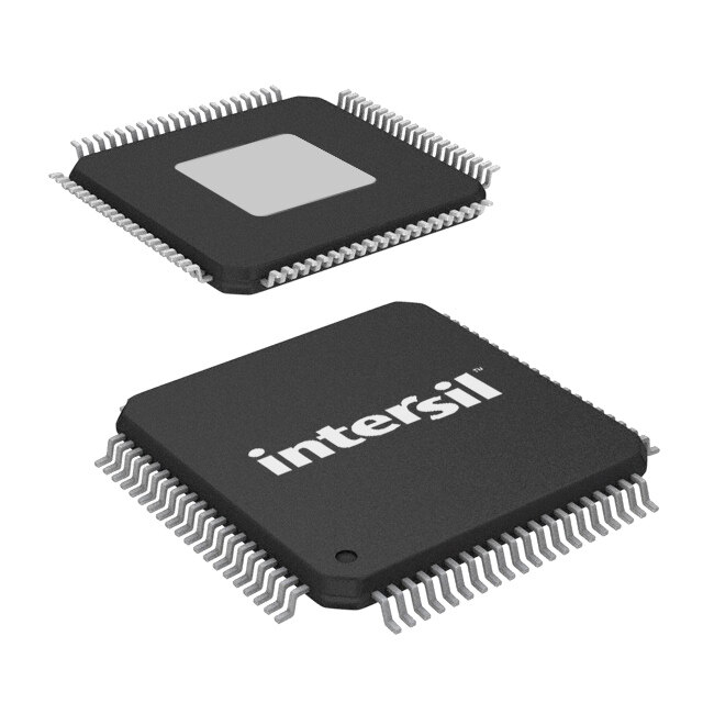
| 产品图片 |
|
| rohs | 符合RoHS无铅 / 符合限制有害物质指令(RoHS)规范要求 |
| 产品系列 | RF集成电路,射频前端,Texas Instruments AFE7225IRGC25- |
| 数据手册 | http://www.ti.com/lit/pdf/slos711a |
| 产品型号 | AFE7225IRGC25 |
| PCN封装 | |
| 产品种类 | 射频前端 |
| 位数 | 12 |
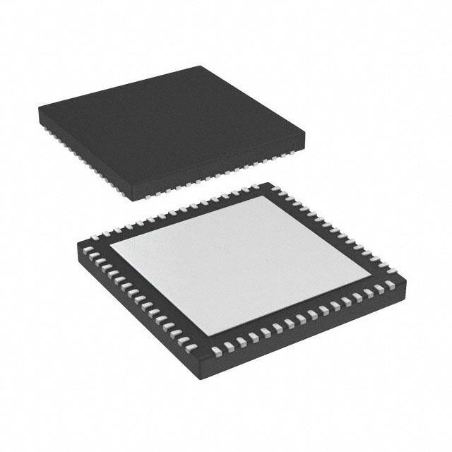
| 供应商器件封装 | 64-VQFN(9x9) |
| 其它名称 | 296-30112-2 |
| 制造商产品页 | http://www.ti.com/general/docs/suppproductinfo.tsp?distId=10&orderablePartNumber=AFE7225IRGC25 |
| 功率(W) | 650mW |
| 包装 | 带卷 (TR) |
| 商标 | Texas Instruments |
| 安装风格 | SMD/SMT |
| 封装 | Reel |
| 封装/外壳 | 64-VFQFN 裸露焊盘 |
| 封装/箱体 | VQFN-64 |
| 工作电源电压 | 1.7 V to 1.9 V, 2.85 V to 3.6 V |
| 工作频率 | 10 kHz |
| 工厂包装数量 | 25 |
| 带宽 | 550 MHz |
| 最大工作温度 | + 85 C |
| 最大数据速率 | 250 MSPs |
| 最小工作温度 | - 40 C |
| 标准包装 | 25 |
| 电压-电源,数字 | 1.7 V ~ 1.9 V |
| 电压-电源,模拟 | 2.85 V ~ 3.6 V |
| 电源电流 | 115 mA |
| 类型 | RF Front End |
| 系列 | AFE7225 |
| 通道数 | 4 |


- 商务部:美国ITC正式对集成电路等产品启动337调查
- 曝三星4nm工艺存在良率问题 高通将骁龙8 Gen1或转产台积电
- 太阳诱电将投资9.5亿元在常州建新厂生产MLCC 预计2023年完工
- 英特尔发布欧洲新工厂建设计划 深化IDM 2.0 战略
- 台积电先进制程称霸业界 有大客户加持明年业绩稳了
- 达到5530亿美元!SIA预计今年全球半导体销售额将创下新高
- 英特尔拟将自动驾驶子公司Mobileye上市 估值或超500亿美元
- 三星加码芯片和SET,合并消费电子和移动部门,撤换高东真等 CEO
- 三星电子宣布重大人事变动 还合并消费电子和移动部门
- 海关总署:前11个月进口集成电路产品价值2.52万亿元 增长14.8%


PDF Datasheet 数据手册内容提取
AFE7222 AFE7225 www.ti.com SLOS711A–NOVEMBER2011–REVISEDDECEMBER2011 Analog Front End Wideband Mixed-Signal Transceiver CheckforSamples:AFE7222,AFE7225 1 INTRODUCTION 1.1 FEATURES 1 • AFE7225 – TXPathInterpolationby2or4 – Dual12-Bit250MSPSTXDACs – RXPathDecimationby2 – Dual12-Bit125MSPSRXADCs – 3.0V/1.8VSupplies,LowPower • AFE7222 – FastWakeupModesforHalf-Duplex – Dual12-Bit130MSPSTXDACs – CoarseorFineDigitalMixer – Dual12-Bit65MSPSRXADCs – QuadratureModulationCorrections • OPTIONS – ClockInputDivide/Multiply – Dual12-BitAuxiliaryDACs – SerialLVDSorInterleavedParallelCMOS Interface – DualInput12-BitAuxiliaryADC – 64-PinQFNPackage(9mm ×9mm) 1.2 APPLICATIONS • Portable,LowPowerRadio • WirelessInfrastructure • Point-to-PointRadio • Pico-CellBTS 1.3 DESCRIPTION The AFE7225/7222 is an analog front end designed for full- or half-duplex radios. Over-sampling transmit 12-bit DACs provide output frequencies from baseband to Nyquist. Under-sampling receive 12-bit ADCs allow analog inputs from baseband to ~230MHz. Most blocks within the AFE7225/7222 are independently controlled for optimization of power consumption versus utilization. Two auxiliary control 12-bit DACs and a dual input auxiliary monitoring 12-bit ADC are available via serial interface. Digital features include QMC (quadrature modulation correction), interpolation, decimation, RMS/peak power meter and mixers with independentNCOsforRXandTXpath. The AFE7225/7222 is available in a 64-pin 9x9mm QFN package (RGC). The AFE7225/7222 is built on Texas Instrument’s low power analog CMOS process and is specified over the full industrial temperature range(–40°Cto85°C). 1 Pleasebeawarethatanimportantnoticeconcerningavailability,standardwarranty,anduseincriticalapplicationsofTexas Instrumentssemiconductorproductsanddisclaimerstheretoappearsattheendofthisdatasheet. PRODUCTIONDATAinformationiscurrentasofpublicationdate.Productsconformto Copyright©2011,TexasInstrumentsIncorporated specifications per the terms of the Texas Instruments standard warranty. Production processingdoesnotnecessarilyincludetestingofallparameters.
AFE7222 AFE7225 SLOS711A–NOVEMBER2011–REVISEDDECEMBER2011 www.ti.com Thesedeviceshavelimitedbuilt-inESDprotection.Theleadsshouldbeshortedtogetherorthedeviceplacedinconductivefoam duringstorageorhandlingtopreventelectrostaticdamagetotheMOSgates. 1.4 DETAILED BLOCK DIAGRAM IIIINNNNNPNP____BAAB____AAAADDDDCCCC RRXX11AA22DDbbCC AB QMCOffset QMCGain/Phase ±Fs/4CoarseMixer FineMixer /2HBFDecimation erialLVDSorarallelCMOS AVD1OD2u3-tB_pAiutUtAsXD C= 3 V SP VCM SYNC SYNC SYNC AVDD3_DAC = 3 V ADC CLK RX RMS/ SYNC DVDD18_DAC=1.8V Peak NCO CLKINP Clock Power Meter AVDD18_ADC=1.8V CLKINN Divide/Multiply SYNC SYNCSYNC RIenfteerrennacle DVDD18=1.8V DAC CLK BIASJ SYNC NCO DVDD18_CLK=1.8V IIIIOOOOUUUUTTTTNNPP____AABB____DDDDAAAACCCC TTXX 11DD22AAbbCC AB QMCOffset InverseSINC QMCGain/Phase ±Fs/4CoarseMixer FineMixer 2xHBFInterpolation 2xHBFInterpolation SerialLVDSorParallelCMOS(8deepFIFO) The1Irnm2p-aBult iPts DadAC=Ground SYNC SYNC SYNC SYNC AUXDAC_A 12bAux DAC SYNC SYNC SYNC AUXDAC_B 12bAux DAC SEN SCLK SDATA SPI Interface,Registers and Control AUXADC_A 2-1 12bAuxADC SDOUT AUXADC_B MUX RESET PDN SYNC Figure1-1.BlockDiagramofAFE7222/AFE7225 2 INTRODUCTION Copyright©2011,TexasInstrumentsIncorporated SubmitDocumentationFeedback ProductFolderLink(s):AFE7222AFE7225
AFE7222 AFE7225 www.ti.com SLOS711A–NOVEMBER2011–REVISEDDECEMBER2011 2 DEVICE INFORMATION 2.1 PACKAGE/ORDERING INFORMATION SPECIFIED TRANSPORT PACKAGE PACKAGE ORDERING PRODUCT PACKAGE-LEAD TEMPERATURE MEDIA, DESIGNATOR MARKING NUMBER RANGE QUANTITY AFE7222IRGCT TapeandReel AFE7222 QFN-64 RGC –40°Cto85°C AFE7222I AFE7222IRGCR TapeandReel AFE7222IRGC25 TapeandReel AFE7225IRGCT TapeandReel AFE7225 QFN-64 RGC –40°Cto85°C AFE7225I AFE7225IRGCR TapeandReel AFE7225IRGC25 TapeandReel 2.2 DEVICE PINOUT, CMOS INPUT/OUTPUT MODE RGC Package (Top View) C C D D 0 1 2 3 4 5 A A A A A A A A D18_ D18_ ET UT K TA DAT DAT DAT DAT DAT DAT D18 D M D S O L A N N C C C C C C D V C V E D C D E D D D D D D D V A V A R S S S S P A A A A A A D 6463 62 61 60 59 58 57 56 55 54 53 52 51 50 49 AVDD18_ADC 1 48 ADCDATA6 INN_B_ADC 2 47 ADC_DCLKOUT INP_B_ADC 3 46 ADCDATA7 Thermal pad connected to ground AVDD18_ADC 4 45 ADCDATA8 INN_A_ADC 5 44 ADCDATA9 INP_A_ADC 6 43 ADCDATA10 AVDD18_ADC 7 42 ADCDATA11 CLKINN 8 6464-QQFNFN 41 DVDD18 CLKINP 9 40 SYNCIN DVDD18_CLK 10 39 DACDATA0 AVDD3_DAC 11 38 DACDATA1 IOUTP_A_DAC 12 37 DACDATA2 IOUTN_A_DAC 13 36 DACDATA3 AVDD3_DAC 14 35 DACDATA4 IOUTP_B_DAC 15 34 DAC_DCLKIN IOUTN_B_DAC 16 33 DACDATA5 17 18 19 20 21 22 23 24 25 26 27 28 29 30 31 32 C J C A B X A B C 1 0 9 8 7 6 8 3_DA BIAS 8_DA DAC_ DAC_ 3_AU ADC_ ADC_ 8_AD ATA1 ATA1 DATA DATA DATA DATA VDD1 D 1 X X D X X 1 D D C C C C D D D U U D U U D C C A A A A V D A A V A A D A A D D D D A V A V D D D A Figure2-1.DevicePinout,CMOSInput/OutputMode Copyright©2011,TexasInstrumentsIncorporated DEVICEINFORMATION 3 SubmitDocumentationFeedback ProductFolderLink(s):AFE7222AFE7225
AFE7222 AFE7225 SLOS711A–NOVEMBER2011–REVISEDDECEMBER2011 www.ti.com Table2-1. PinConfiguration:CMOSInput/OutputMode PIN DESCRIPTION NO. NAME 1 AVDD18_ADC 1.8VsupplyforRXADCs 2 INN_B_ADC RXADCchannelBanaloginput,negative 3 INP_B_ADC RXADCchannelBanaloginput,positive 4 AVDD18_ADC 1.8VsupplyforRXADCs 5 INN_A_ADC RXADCchannelAanaloginput,negative 6 INP_A_ADC RXADCchannelAanaloginput,positive 7 AVDD18_ADC 1.8VsupplyforRXADCs 8 CLKINN mainclockinput,negativesideifdifferentialmode,TXsideifsingle-ended2clockmode 9 CLKINP mainclockinput,positivesideifdifferentialmode,RXsideifsingle-ended2clockmode 10 DVDD18_CLK 1.8VsupplyforClockingcircuit 11 AVDD3_DAC 3VsupplyforTXDACs 12 IOUTP_A_DAC TXDACchannelAcurrentoutput,positive(currentsinkDACs) 13 IOUTN_A_DAC TXDACchannelAcurrentoutput,negative(currentsinkDACs) 14 AVDD3_DAC 3VsupplyforTXDACs 15 IOUTP_B_DAC TXDACchannelBcurrentoutput,positive(currentsinkDACs) 16 IOUTN_B_DAC TXDACchannelBcurrentoutput,negative(currentsinkDACs) 17 AVDD3_DAC 3VsupplyforTXDACs setstheTXDACoutputcurrent(resistorfrompintoground).Use960Ohmtosetafullscalecurrentof 18 BIASJ 20mA. 19 DVDD18_DAC 1.8VDACdigitalsupply 20 AUXDAC_A auxiliaryDACchannelAoutput,currentsourcingupto7.5mA(SPIprogrammable) 21 AUXDAC_B auxiliaryDACchannelBoutput,currentsourcingupto7.5mA(SPIprogrammable) 22 AVDD3_AUX 3VsupplyforauxiliaryADC/DACs 23 AUXADC_A auxiliaryADCchannelAinput 24 AUXADC_B auxiliaryADCchannelBinput 25 AVDD18_ADC 1.8VsupplyforRXADCs 26 DACDATA11 CMOSdatainputforTXdata,MSBofTXDACs 27 DACDATA10 CMOSdatainputforTXdata 28 DACDATA9 CMOSdatainputforTXdata 29 DACDATA8 CMOSdatainputforTXdata 30 DACDATA7 CMOSdatainputforTXdata 31 DACDATA6 CMOSdatainputforTXdata 32 DVDD18 1.8Vsupplyfordigitalinterface 33 DACDATA5 CMOSdatainputforTXdata 34 DAC_DCLKIN CMOSclockinputforTXdata.Sendclockwithdata. 35 DACDATA4 CMOSdatainputforTXdata 36 DACDATA3 CMOSdatainputforTXdata 37 DACDATA2 CMOSdatainputforTXdata 38 DACDATA1 CMOSdatainputforTXdata 39 DACDATA0 CMOSdatainputforTXdata.LSBofTXDACs 40 SYNCIN CMOSsyncinput.UsedtoresetinternalclockdividersandresetTXdataFIFOpointer 41 DVDD18 1.8Vsupplyfordigitalinterface 42 ADCDATA11 CMOSdataoutputforRXdata,MSBofRXADCs 43 ADCDATA10 CMOSdataoutputforRXdata 44 ADCDATA9 CMOSdataoutputforRXdata 45 ADCDATA8 CMOSdataoutputforRXdata 46 ADCDATA7 CMOSdataoutputforRXdata 4 DEVICEINFORMATION Copyright©2011,TexasInstrumentsIncorporated SubmitDocumentationFeedback ProductFolderLink(s):AFE7222AFE7225
AFE7222 AFE7225 www.ti.com SLOS711A–NOVEMBER2011–REVISEDDECEMBER2011 Table2-1. PinConfiguration:CMOSInput/OutputMode(continued) PIN DESCRIPTION NO. NAME 47 ADC_DCLKOUT CMOSclockoutputforRXdata 48 ADCDATA6 CMOSdataoutputforRXdata 49 DVDD18 1.8Vsupplyfordigitalinterface 50 ADCDATA5 CMOSdataoutputforRXdata 51 ADCDATA4 CMOSdataoutputforRXdata 52 ADCDATA3 CMOSdataoutputforRXdata 53 ADCDATA2 CMOSdataoutputforRXdata 54 ADCDATA1 CMOSdataoutputforRXdata 55 ADCDATA0 CMOSdataoutputforRXdata,LSBofRXADCs Canbeprogrammedasglobalpowerdown(deepsleep),fastrecoverypowerdown(lightsleep)orTX/RX 56 PDN switch.Activehigh. 57 SEN SPIenable(1.8VCMOS) 58 SDATA SPIdatainput(1.8VCMOS) 59 SCLK SPIclockinput(1.8VCMOS) 60 SDOUT SPIdataoutput(1.8VCMOS) 61 RESET ResettheSPI.Activehigh(1.8VCMOS). 62 AVDD18_ADC 1.8VsupplyforRXADCs Commonmodevoltageoutput.OutputstheidealcommonmodeinputvoltagefortheADC.Nominally 63 VCM around0.95V. 64 AVDD18_ADC 1.8VsupplyforRXADCs Thermal VSS Connectthermalpadtotheboardground pad Copyright©2011,TexasInstrumentsIncorporated DEVICEINFORMATION 5 SubmitDocumentationFeedback ProductFolderLink(s):AFE7222AFE7225
AFE7222 AFE7225 SLOS711A–NOVEMBER2011–REVISEDDECEMBER2011 www.ti.com 2.3 DEVICE PINOUT, LVDS INPUT/OUTPUT MODE RGC Package (Top View) P N P N P N T T C C _1 _1 _0 _0 U U D D A A A A O O A A T T T T K K 18_ 18_ T T A _DA _DA _DA _DA DCL DCL 18 D D E U K T A A A A _ _ D D M D S O L A N N C C C C C C D V C V E D C D E D D D D D D D V A V A R S S S S P A A A A A A D 6463 62 61 60 59 58 57 56 55 54 53 52 51 50 49 AVDD18_ADC 1 48 NC INN_B_ADC 2 47 ADC_FCLKOUTP INP_B_ADC 3 46 ADC_FCLKOUTN Thermal pad connected to ground AVDD18_ADC 4 45 ADCB_DATA_0P INN_A_ADC 5 44 ADCB_DATA_0N INP_A_ADC 6 43 ADCB_DATA_1P AVDD18_ADC 7 42 ADCB_DATA_1N CLKINN 8 64-QQFNFN 41 DVDD18 CLKINP 9 40 SYNCINN DVDD18_CLK 10 39 SYNCINP AVDD3_DAC 11 38 DACB_DATA_1N IOUTP_A_DAC 12 37 DACB_DATA_1P IOUTN_A_DAC 13 36 DACB_DATA_0N AVDD3_DAC 14 35 DACB_DATA_0P IOUTP_B_DAC 15 34 DAC_DCLKINN IOUTN_B_DAC 16 33 DAC_DCLKINP 1718 19 20 21 22 23 24 25 26 27 28 29 30 31 32 C J C A B X A B C P N P N P N 8 A S A _ _ U _ _ D 1 1 0 0 N N 1 AVDD3_D BIA DVDD18_D AUXDAC AUXDAC AVDD3_A AUXADC AUXADC AVDD18_A ACA_DATA_ ACA_DATA_ ACA_DATA_ ACA_DATA_ DAC_FCLKI DAC_FCLKI DVDD D D D D Figure2-2.DevicePinout,LVDSInput/OutputMode Table2-2.PinConfiguration:LVDSInput/OutputMode PIN DESCRIPTION NO. NAME 1 AVDD18_ADC 1.8VsupplyforRXADCs 2 INN_B_ADC RXADCchannelBanaloginput,negative 3 INP_B_ADC RXADCchannelBanaloginput,positive 4 AVDD18_ADC 1.8VsupplyforRXADCs 5 INN_A_ADC RXADCchannelAanaloginput,negative 6 INP_A_ADC RXADCchannelAanaloginput,positive 7 AVDD18_ADC 1.8VsupplyforRXADCs 8 CLKINN mainclockinput,negativesideifdifferentialmode,TXsideifsingle-ended2clockmode 6 DEVICEINFORMATION Copyright©2011,TexasInstrumentsIncorporated SubmitDocumentationFeedback ProductFolderLink(s):AFE7222AFE7225
AFE7222 AFE7225 www.ti.com SLOS711A–NOVEMBER2011–REVISEDDECEMBER2011 Table2-2.PinConfiguration:LVDSInput/OutputMode(continued) PIN DESCRIPTION NO. NAME 9 CLKINP mainclockinput,positivesideifdifferentialmode,RXsideifsingle-ended2clockmode 10 DVDD18_CLK 1.8VsupplyforClockingcircuit 11 AVDD3_DAC 3VsupplyforTXDACs 12 IOUTP_A_DAC TXDACchannelAcurrentoutput,positive(currentsinkDACs) 13 IOUTN_A_DAC TXDACchannelAcurrentoutput,negative(currentsinkDACs) 14 AVDD3_DAC 3VsupplyforTXDACs 15 IOUTP_B_DAC TXDACchannelBcurrentoutput,positive(currentsinkDACs) 16 IOUTN_B_DAC TXDACchannelBcurrentoutput,negative(currentsinkDACs) 17 AVDD3_DAC 3VsupplyforTXDACs setstheTXDACoutputcurrent(resistorfrompintoground).Use960Ohmtosetafullscalecurrentof 18 BIASJ 20mA. 19 DVDD18_DAC 1.8VDACdigitalsupply 20 AUXDAC_A auxiliaryDACchannelAoutput,currentsourcingupto7.5mA(SPIprogrammable) 21 AUXDAC_B auxiliaryDACchannelBoutput,currentsourcingupto7.5mA(SPIprogrammable) 22 AVDD3_AUX 3VsupplyforauxiliaryADC/DACs 23 AUXADC_A auxiliaryADCchannelAinput 24 AUXADC_B auxiliaryADCchannelBinput 25 AVDD18_ADC 1.8VsupplyforRXADCs 26,27 LVDSWire1datainputforChannelATXdata–inactivein1-wiremode,LSBbytein2-wiremode 26 DAC_DATA_11 Positive 27 DAC_DATA_10 Negative 28,29 LVDSWire0datainputforChannelATXdata–activein1-wiremode,MSBbytein2-wiremode 28 DAC_DATA_9 Positive 29 DAC_DATA_8 Negative 30,31 LVDSframeclockinput 30 DAC_FCLKINP Positive 31 DAC_FCLKINN Negative 32 DVDD18 1.8Vsupplyfordigitalinterface 33,34 LVDSbitclockinput 33 DAC_DCLKINP Positive 34 DAC_DCLKINN Negative 35,36 LVDSWire0datainputforChannelBTXdata–activein1-wiremode,LSBbytein2-wiremode 35 DACB_DATA_0P Positive 36 DACB_DATA_0N Negative 37,38 LVDSWire1datainputforChannelBTXdata–inactivein1-wiremode,MSBbytein2-wiremode 37 DACB_DATA_1P Positive 38 DACB_DATA_1N Negative 39,40 LVDSSYNCinput–UsedtoresetinternalclockdividersandresetTXdataFIFOpointer 39 SYNCINP Positive 40 SYNCINN Negative 41 DVDD18 1.8Vsupplyfordigitalinterface 42,43 LVDSWire1dataoutputforChannelBRXdata–inactivein1-wiremode,MSBbytein2-wiremode 42 ADCB_DATA_1N Positive 43 ADCB_DATA_1P Negative 44,45 LVDSWire0dataoutputforChannelBRXdata–activein1-wiremode,LSBbytein2-wiremode 44 ADCB_DATA_0N Positive 45 ADCB_DATA_0P Negative Copyright©2011,TexasInstrumentsIncorporated DEVICEINFORMATION 7 SubmitDocumentationFeedback ProductFolderLink(s):AFE7222AFE7225
AFE7222 AFE7225 SLOS711A–NOVEMBER2011–REVISEDDECEMBER2011 www.ti.com Table2-2.PinConfiguration:LVDSInput/OutputMode(continued) PIN DESCRIPTION NO. NAME 46,47 LVDSframeclockoutput 46 ADC_FCLKOUTN Positive 47 ADC_FCLKOUTP Negative 48 NC NoConnect 49 DVDD18 1.8Vsupplyfordigitalinterface 50,51 LVDSbitclockoutput 50 ADC_DCLKOUTN Positive 51 ADCDCLKOUTP Negative 52,53 LVDSWire0dataoutputforChannelARXdata–activein1-wiremode,MSBbytein2-wiremode 52 ADCA_DATA_0N Positive 53 ADCA_DATA_0P Negative 54,55 LVDSWire1dataoutputforChannelARXdata–inactivein1-wiremode,LSBbytein2-wiremode 54 ADCA_DATA_1N Positive 55 ADCA_DATA_1P Negative Canbeprogrammedasglobalpowerdown(deepsleep),fastrecoverypowerdown(lightsleep)orTX/RX 56 PDN switch.Activehigh. 57 SEN SPIenable(1.8VCMOS) 58 SDATA SPIdatainput(1.8VCMOS) 59 SCLK SPIclockinput(1.8VCMOS) 60 SDOUT SPIdataoutput(1.8VCMOS) 61 RESET ResettheSPI.Activehigh(1.8VCMOS). 62 AVDD18_ADC 1.8VsupplyforRXADCs Commonmodevoltageoutput.OutputstheidealcommonmodeinputvoltagefortheADC.Nominally 63 VCM around0.95V. 64 AVDD18_ADC 1.8VsupplyforRXADCs Thermal VSS Connectthermalpadtotheboardground pad 8 DEVICEINFORMATION Copyright©2011,TexasInstrumentsIncorporated SubmitDocumentationFeedback ProductFolderLink(s):AFE7222AFE7225
AFE7222 AFE7225 www.ti.com SLOS711A–NOVEMBER2011–REVISEDDECEMBER2011 3 ELECTRICAL SPECIFICATIONS 3.1 ABSOLUTE MAXIMUM RATINGS(1) overoperatingfree-airtemperaturerange(unlessotherwisenoted) MIN MAX UNIT Supplyvoltagerange,*VDD3* –0.3 3.6 V Supplyvoltagerange,*VDD18* –0.3 2.1 V Voltagebetweeen*VDD3*to*VDD18* –2.4 3.9 V INP_A_ADC,INM_A_ADC,INP_B_ADC,INM_B_ADC,AUXADC_A,AUXADC_B,CLKINN,CLKINP –0.3 2.1 V RESET,SCLK,SDATASEN –0.3 3.9 V DAC*_DATA_nP/M,DAC_DCLK –0.3 2.1 V T Operatingfree-airtemperaturerange –40 85 °C A T Operatingjunctiontamperaturerange 125 °C J T Storagetemperaturerange –65 150 °C stg ESDratingHumanBodyModel(HBM) 2 kV (1) Stressesbeyondthoselistedunderabsolutemaximumratingsmaycausepermanentdamagetothedevice.Thesearestressratings onlyandfunctionaloperationofthedeviceattheseoranyotherconditionsbeyondthoseindicatedunderrecommendedoperating conditionsisnotimplied.Exposuretoabsolutemaximumratedconditionsforextendedperiodsmayaffectdevicereliability. 3.2 THERMAL INFORMATION AFE7222/AFE7225 THERMALMETRIC RGCPACKAGE UNITS 64PINS θ Junction-to-ambientthermalresistance 22.8 JA θ Junction-to-case(top)thermalresistance 6.7 JCtop θ Junction-to-boardthermalresistance 2.3 JB °C/W ψ Junction-to-topcharacterizationparameter 0.1 JT ψ Junction-to-boardcharacterizationparameter 2.2 JB θ Junction-to-case(bottom)thermalresistance 0.2 JCbot 3.3 RECOMMENDED OPERATING CONDITIONS overoperatingfree-airtemperaturerange(unlessotherwisenoted) AFE7222 AFE7225 PARAMETER TESTCONDITIONS UNIT MIN TYP MAX MIN TYP MAX DVDD18voltagerange 1.7 1.8 1.9 1.7 1.8 1.9 V AVDD3voltagerange 2.85 3.0 3.6 2.85 3.0 3.6 V Commonmodevoltageat VCM-0.05 VCM VCM+0.05 VCM–0.05 VCM VCM+0.05 V ADCinputpins Commonmodevoltageat AVDD3 AVDD3 V DACoutputpins ADC_CLKspeed(1) 2.5 65 2.5 125 MSPS DAC_CLKspeed(1) 1 130 1 250 MSPS (1) SeeTable10-1andTable10-2forcorrespondingmaximuminterfacerates. Copyright©2011,TexasInstrumentsIncorporated ELECTRICALSPECIFICATIONS 9 SubmitDocumentationFeedback ProductFolderLink(s):AFE7222AFE7225
AFE7222 AFE7225 SLOS711A–NOVEMBER2011–REVISEDDECEMBER2011 www.ti.com 3.4 SUPPLY CHARACTERISTICS AVDD18_ADC=1.8V,DVDD18_CLK=1.8V,DVDD18=1.8V,DVDD18_DAC=1.8V,AVDD3_DAC=3.0V,AVDD3_AUX=3.0V, IOUTFS=20mA,typicalvaluesatT =25°C,fulltemperaturerangeisT =–40°CtoT =85°C,unlessotherwisenoted. A MIN MAX PARAMETER TESTCONDITIONS AFE7222 AFE7225 DualRXADC,DualTXDAC DualRXADC,DualTX withInterpolateby2,CMOS DACwithInterpolateby2, interface 2-wireLVDSinterface FADCCLK=65MSPS FADCCLK=125MSPS UNIT fADCIN=10MHz fADCIN=10MHz FDACCLK=130MSPS FDACCLK=250MSPS fDACOUT=10MHz fDACOUT=10MHz MIN TYP MAX MIN TYP MAX RXandTXactive. Powerdissipation,fullduplexmode 545 610 577 650 mW NoinputsignalappliedonADCandDAC RXactive,TXinlightsleep,TXclockis Powerdissipation,halfduplexRXmode off. 360 420 362 417 mW NoinputsignalappliedonADCandDAC TXactive,RXinlightsleep,RXclockis Powerdissipation,halfduplexTXmode on. 338 370 419 482 mW NoinputsignalappliedonADCandDAC Globalpowerdownenabled 12 40 12 40 Fastrecoverypowerdownenabled, 140 165 215 246 TX/RXsleeping,clockson PowerdissipationinSleepmodes mW Fastrecoverypowerdownenabled, TX/RXsleeping,TXclockoff,RXclock 120 165 177 231 on. Differentialinputclock 25 25 Globalpowerdown,RXrecoverytime µs Single-endedinputclock 20 20 GlobalpowerdowninLowpowerRX Differentialinputclock 25 25 CMOSmode,RXrecoverytime(ADC µs runningatlessthan40MSPS) Single-endedinputclock 13 13 Differentialinputclock 25 25 Globalpowerdown,TXrecoverytime µs Single-endedinputclock 5 5 RXrecoverytimeinfastrecoverymode RXclockisONduringpowerdown 5 5 µs TXrecoverytimeinfastrecoverymode 5 5 µs RXrecoverytimefromRXpowerdown RXclockisonduringpowerdown 5 5 µs TXrecoverytimefromTXpowerdown 5 5 µs 10 ELECTRICALSPECIFICATIONS Copyright©2011,TexasInstrumentsIncorporated SubmitDocumentationFeedback ProductFolderLink(s):AFE7222AFE7225
AFE7222 AFE7225 www.ti.com SLOS711A–NOVEMBER2011–REVISEDDECEMBER2011 3.5 RX ADC ELECTRICAL CHARACTERISTICS TypicalvaluesatT =25°C,fulltemperaturerangeisT =–40°CtoT =85°C,suppliesatnominalvoltages,50%clock A MIN MAX dutycycle,LVDSoutputinterface,–1dBFSdifferentialinput,unlessotherwisenoted. AFE7222 AFE7225 PARAMETER TESTCONDITIONS UNIT MIN TYP MAX MIN TYP MAX MaximumClockRate 65 125 MSPS Resolution 12 12 bits ANALOGINPUTS Differentialinputrange 2 2 Vpp V Commonmodeoutputvoltage 0.95 0.95 V CM Inputresistance(DC) Differential >1 >1 MΩ Inputcapacitance Differential 4 4 pF Analoginputbandwidth 550 550 MHz CMRR Commonmoderejectionratio Fin=10MHz 40 40 dB DYNAMICACCURACY NoMissingCodes, DNL Differentiallinearityerror –0.95 ±0.5 1.4 –0.95 ±0.5 1.4 LSB Fin=10MHz INL Integrallinearityerror Fin=10MHz –1.7 ±0.2 1.7 –1.7 ±0.2 1.7 LSB Offseterror –15 2 15 –15 3 15 mV Offsettemperatureco-efficient >0.005 >0.005 mV/°C Gainerrorasaresultofinternalreference –2.5 2.5 –2.5 2.5 %FS inaccuracyalone–EGREF Gainerrorofchannelalone–EGCHAN ±1 ±1 %FS DYNAMICACCHARACTERISTICS Fin=10MHz 67.5 70.5 67 70.7 dBFS SNR Signal-to-noiseratio(1) Fin=70MHz 70 70.1 dBFS Fin=140MHz 68.7 69.5 dBFS Fin=10MHz 73 85 73 84 dBc SFDR Spuriousfreedynamicrange(1) Fin=70MHz 81 79 dBc Fin=140MHz 77 76 dBc (1) Upto65MSPStypicalSNRandSFDRperformanceinCMOSinterfaceissameaswithLVDSinterface. Copyright©2011,TexasInstrumentsIncorporated ELECTRICALSPECIFICATIONS 11 SubmitDocumentationFeedback ProductFolderLink(s):AFE7222AFE7225
AFE7222 AFE7225 SLOS711A–NOVEMBER2011–REVISEDDECEMBER2011 www.ti.com 3.6 TX DAC ELECTRICAL CHARACTERISTICS TypicalvaluesatT =25°C,fulltemperaturerangeisT =–40°CtoT =85°C,50%clockdutycycle,suppliesatnominal A MIN MAX voltages,I =20mA,DACoutputcommonmodevoltageisAVDD3=3.0V,unlessotherwisenoted. OUTFS AFE7222 AFE7225 PARAMETER TESTCONDITIONS UNIT MIN TYP MAX MIN TYP MAX Maximumclockoutputrate 130 250 MSPS Resolution 12 12 Bits ANALOGOUTPUTS Fullscaleoutputcurrent,perDAC 2 20 2 20 mA Outputvoltagecompliancerange IOUTFS=20mA, AVDD3_DAC–0.5 AVDD3_DAC+0.5 AVDD3_DAC–0.5 AVDD3_DAC+0.5 V Currentsinkoutput Outputresistance 300 300 kΩ Outputcapacitance 5 5 pF Offseterror Midcodeoffset ±0.03 ±0.03 %FS(1) Gainerror Internalreference ±1 ±1 %FS(1) Gainmismatch InternalreferencedualDAC ±0.5 ±0.5 %FS(1) DCPERFORMANCE INL Integralnon-linearity Fout=10MHz –2 ±1 2 –2 ±1 2 LSB DNL Differentialnon-linearity Fout=10MHz ±0.5 ±0.5 LSB ACPERFORMANCE Noisespectraldensity Fout=10MHz,0dBFS 145.5 149 148.5 151 dBc/Hz Fout=10MHz,0dBFS 70 76 70 76 dBc SFDR Spuriousfreedynamicrange Fout=20MHz,0dBFS 75 74 dBc Fout=5.1/6.1MHz, IMD Inter-modulationdistortion 73 73 dBc –7dBFSeach DACclock=122.88MSPS, 75 Fout=30.72MHz ACLR Adjacentchannelleakageratio dB DACclock=245.76MSPS, 73 Fout=61.44MHz (1) %FS=%DifferentialFullScale 3.7 AUXILIARY ADC ELECTRICAL CHARACTERISTICS TypicalvaluesatT =25°C,fulltemperaturerangeisT =–40°CtoT =85°C,suppliesatnominalvoltages,unless A MIN MAX otherwisenoted. PARAMETER TESTCONDITIONS AFE7222/AFE7225 UNIT MIN TYP MAX MaximumClockRate 100 kSPS Resolution 12 Bits ANALOGINPUTS Inputvoltagerange 1.5 V Inputcapacitance 4 pF Maximuminputsignalfrequency 10 kHz DCPERFORMANCE INL Integralnon-linearity Staticconditions(nearDCinput) –4.5 ±2 4.5 LSB 12 ELECTRICALSPECIFICATIONS Copyright©2011,TexasInstrumentsIncorporated SubmitDocumentationFeedback ProductFolderLink(s):AFE7222AFE7225
AFE7222 AFE7225 www.ti.com SLOS711A–NOVEMBER2011–REVISEDDECEMBER2011 3.8 AUXILIARY DAC ELECTRICAL CHARACTERISTICS TypicalvaluesatT =25°C,fulltemperaturerangeisT =–40°CtoT =85°C,suppliesatnominalvoltages,I = A MIN MAX OUTFS 5mA,300Ωtermination,unlessotherwisenoted. AFE7222/AFE7225 PARAMETER TESTCONDITIONS UNIT MIN TYP MAX MaximumClockRate ContinuousrefreshofAUXDACChannelAfromSDATA 3.33(1) MSPS andChannelBfromSDOUT Resolution 12 Bits ANALOGOUTPUTS Outputcurrent,perauxDAC 2.5 7.5 mA Outputvoltagecompliancerange 1.5 V DYNAMICPERFORMANCE INL Integralnon-linearity Staticconditions(nearDCinput) –1.7 ±0.5 1.7 LSB DNL Differentialnon-linearity Staticconditions(nearDCinput) ±0.3 LSB (1) 12bitsx(1/SCLK)indirectaccessmode,SCLKmaxlimitis40MHz 3.9 DIGITAL CHARACTERISTICS TheDCspecificationsrefertotheconditionwherethedigitaloutputsarenotswitching,butarepermanentlyatavalidlogic level0or1.AVDD18*,DVDD18*=1.8V,AVDD3*=3.0V PARAMETER TESTCONDITIONS MIN TYP MAX UNIT DIGITALINPUTS–RESET,SCLK,SDATA,SEN,PDN Allthesepinssupport1.8Vand3VCMOS High-levelinputvoltage 1.3 V logiclevels. Low-levelinputvoltage 0.4 V DACDIGITALINPUTSINCMOSINTERFACEMODE High-levelinputvoltage 1.8VCMOSlogiclevelsonly 1.3 V Low-levelinputvoltage 0.4 V DACDIGITALINPUTSINLVDSINTERFACEMODE StandardswingLVDSwithexternal100ohms V High-leveldifferentialinputvoltage 350 mV IDH termination StandardswingLVDSwithexternal100ohms V Low-leveldifferentialinputvoltage –350 mV IDL termination V Inputcommon-modevoltage 1.2 V ICM DIGITALOUTPUTS–CMOSINTERFACE–SDOUT,ADCOUTPUTS(INCMOSINTERFACEMODE) High-leveloutputvoltage DVDD18–0.1 DVDD18 V Low-leveloutputvoltage 0 0.1 V DIGITALOUTPUTS–LVDSINTERFACE(ADCOUTPUTSINLVDSMODE) V High-leveldifferentialoutputvoltage StandardswingLVDS 235 375 mV ODH V Low-leveldifferentialoutputvoltage StandardswingLVDS –375 –235 mV ODL V Outputcommon-modevoltage 0.9 1.05 1.2 V OCM Copyright©2011,TexasInstrumentsIncorporated ELECTRICALSPECIFICATIONS 13 SubmitDocumentationFeedback ProductFolderLink(s):AFE7222AFE7225
AFE7222 AFE7225 SLOS711A–NOVEMBER2011–REVISEDDECEMBER2011 www.ti.com 3.10 TIMING REQUIREMENTS TypicalvaluesatT =25°C,fulltemperaturerangeisT =–40°CtoT =85°C,unlessotherwisenoted. A MIN MAX AFE7222 AFE7225 PARAMETER TESTCONDITIONS UNIT MIN TYP MAX MIN TYP MAX SCLKINPUT t CLOCKperiod 25 25 ns SCLK t CLOCKpulsewidthhigh 12.5 12.5 ns SCLKH Assuming50/50dutycycle t CLOCKpulsewidthlow 12.5 12.5 ns SCLKL 3.11 TIMING REQUIREMENTS FOR RECEIVE PATH – LVDS AND CMOS MODES Typicalvaluesareat25°C,AVDD3_DAC=3.0V,AVDD3_AUX=3.0V,AVDD18_ADC=1.8V,DVDD18_CLK=1.8V, DVDD18_DAC=1.8V,DVDD18=1.8V,samplingfrequency=125MSPS,sinewaveinputclock,1.5V clockamplitude, pp C =5pF (1),R =100Ω (2),unlessotherwisenoted.MinandmaxvaluesareacrossthefulltemperaturerangeT = LOAD LOAD MIN -40°CtoT =85°C,AVDD3_DAC=3.0V,AVDD3_AUX=3.0V,AVDD18_ADC=1.8V,DVDD18_CLK=1.8V, MAX DVDD18_DAC=1.8V,DVDD18=1.7Vto1.9V PARAMETER TESTCONDITIONS MIN TYP MAX UNIT T Aperturedelay 2 ns A Aperturedelaymatching Betweentwochannelsonthesamedevice ±120 ps Aperturedelaymatching BetweentwodevicesatsametemperatureandDVDD18supply ±450 ps Jitteraddedbyinternalclockdistribution,specifiedasitrelates T Aperturejitter 250 fsrms J tothereceiveADC DefaultMode 16 ADCLatency(3) MixerEnabled(RX_MIXER_EN=1) 33 clock cycles RXQMCGainPhaseCorrectionEnabled 22 (RX_QMC_CORR_ENA=1,RX_QMC_CORR_ENB=1) LVDSOUTPUTINTERFACE 2-WIREMODE,DDRCLOCK(4),Samplingfrequency=125MSPS t Datasetuptime (5) Datavalid(5)tozero-crossingofCLKOUTP 0.29 0.42 ns su t Dataholdtime (5) Zero-crossingofCLKOUTPtodatabecominginvalid (5) 0.3 0.47 ns h t Clockpropagationdelay Inputclockrisingedgecross-overtooutputclockrisingedge t =t ns PDI PDI DELAY cross-over10MSPS≤Samplingfrequency≤125MSPSTs= tdelay 1/Samplingfrequency 11.5 13.8 15.5 ns Variationoft BetweentwodevicesatsametemperatureandDVDD18supply ±300 ps delay Dutycycleofdifferentialclock,(ADC_DCLKOUTP- LVDSbitclockdutycycle ADC_DCLKOUTM)10MSPS≤Samplingfrequency≤125 50% MSPS 2-WIREMODE,SDRCLOCK(4),Samplingfrequency=65MSPS t Datasetuptime (5) Datavalid (5)tozero-crossingofCLKOUTP 0.85 1.08 ns su t Dataholdtime (5) Zero-crossingofCLKOUTPtodatabecominginvalid (5) 1.08 1.21 ns h Inputclockrisingedgecross-overtooutputclockrisingedge t Clockpropagationdelay cross-over10MSPS≤Samplingfrequency≤65MSPSTs= t =0.5*Ts+t ns PDI PDI DELAY 1/Samplingfrequency t 11.5 14 16.5 ns delay Variationoft BetweentwodevicesatsametemperatureandDVDD18supply ±300 ps delay Dutycycleofdifferentialclock,(CLKOUTP-CLKOUTM)10 LVDSbitclockdutycycle 50% MSPS≤Samplingfrequency≤65MSPS 1-WIREMODE(DDRCLOCKONLY)(4),Samplingfrequency=65MSPS t Datasetuptime (5) Datavalid (5)tozero-crossingofCLKOUTP 0.25 0.39 ns su (1) C istheeffectiveexternalsingle-endedloadcapacitancebetweeneachoutputpinandground LOAD (2) R isthedifferentialloadresistancebetweentheLVDSoutputpair. LOAD (3) Athigherfrequencies,t isgreaterthanoneclockperiodandoveralllatency=ADClatency+1. PDI (4) Measurementsaredonewithatransmissionlineof100-Ωcharacteristicimpedancebetweenthedeviceandtheload.Setupandhold timespecificationstakeintoaccounttheeffectofjitterontheoutputdataandclock. (5) DatavalidreferstoLOGICHIGHof+100.0mVandLOGICLOWof-100.0mV. 14 ELECTRICALSPECIFICATIONS Copyright©2011,TexasInstrumentsIncorporated SubmitDocumentationFeedback ProductFolderLink(s):AFE7222AFE7225
AFE7222 AFE7225 www.ti.com SLOS711A–NOVEMBER2011–REVISEDDECEMBER2011 Typicalvaluesareat25°C,AVDD3_DAC=3.0V,AVDD3_AUX=3.0V,AVDD18_ADC=1.8V,DVDD18_CLK=1.8V, DVDD18_DAC=1.8V,DVDD18=1.8V,samplingfrequency=125MSPS,sinewaveinputclock,1.5V clockamplitude, pp C =5pF(1),R =100Ω(2),unlessotherwisenoted.MinandmaxvaluesareacrossthefulltemperaturerangeT = LOAD LOAD MIN -40°CtoT =85°C,AVDD3_DAC=3.0V,AVDD3_AUX=3.0V,AVDD18_ADC=1.8V,DVDD18_CLK=1.8V, MAX DVDD18_DAC=1.8V,DVDD18=1.7Vto1.9V PARAMETER TESTCONDITIONS MIN TYP MAX UNIT t Dataholdtime (5) Zero-crossingofCLKOUTPtodatabecominginvalid (5) 0.26 0.4 ns h Inputclockrisingedgecross-overtooutputclockrisingedge t Clockpropagationdelay cross-over10MSPS≤Samplingfrequency≤65MSPSTs= t =0.5*Ts+t ns PDI PDI DELAY 1/Samplingfrequency t 11.5 13.5 15.5 ns delay Variationoft BetweentwodevicesatsametemperatureandDVDD18supply ±300 ps delay Dutycycleofdifferentialclock,(CLKOUTP-CLKOUTM)10 LVDSbitclockdutycycle 50% MSPS≤Samplingfrequency≤65MSPS COMMON Risetimemeasuredfrom-100mVto+100mVFalltime t , Datarisetime,Datafall RISE measuredfrom+100mVto-100mV10MSPS≤Sampling 0.08 ns t time FALL frequency≤125MSPS Risetimemeasuredfrom-100mVto+100mVFalltime t , Outputclockrisetime, CLKRISE measuredfrom+100mVto-100mV10MSPS≤Sampling 0.1 ns t Outputclockfalltime CLKFALL frequency≤125MSPS CMOSOUTPUTINTERFACE (6),Samplingfrequency=105MSPS(7) t Datasetuptime (8) Datavalidtocross-overofADC_DCLKOUT (8) 0.5 1.4 ns su t Dataholdtime (8) Cross-overofADC_DCLKOUTtodatabecominginvalid (8) 1.4 1.8 ns h Inputclockrisingedgecross-overtooutputclockrisingedge t Clockpropagationdelay cross-over10MSPS≤Samplingfrequency≤105MSPSTs= t =0.5*Ts+t ns PDI PDI DELAY 1/Samplingfrequency t 14 16.5 19 ns delay Variationoft BetweentwodevicesatsametemperatureandDVDD18supply ±350 ps delay Dutycycleofoutputclock,ADC_DCLKOUT10MSPS≤ Outputclockdutycycle 46% Samplingfrequency≤105MSPS Risetimemeasuredfrom20%to80%ofDVDD18Falltime t , Datarisetime,Datafall RISE measuredfrom80%to20%ofDVDD181≤Sampling 0.76 ns t time FALL frequency≤105MSPS Risetimemeasuredfrom20%to80%ofDVDD18Falltime t , Outputclockrisetime, CLKRISE measuredfrom80%to20%ofDRVDD1≤Samplingfrequency 0.74 ns t Outputclockfalltime CLKFALL ≤105MSPS (6) ForFs>105MSPS,itisrecommendedtouseexternalclockfordatacaptureandNOTthedeviceoutputclocksignal (ADC_DCLKOUT). (7) ForFs>65MSPS,CMOSoutputbuffersstrengthisincreasedbywritingserialregisterbitsSTR_CTRL<1:0>='10'. (8) DatavalidreferstoLOGICHIGHof1.26VandLOGICLOWof0.54V. Copyright©2011,TexasInstrumentsIncorporated ELECTRICALSPECIFICATIONS 15 SubmitDocumentationFeedback ProductFolderLink(s):AFE7222AFE7225
AFE7222 AFE7225 SLOS711A–NOVEMBER2011–REVISEDDECEMBER2011 www.ti.com Table3-1.LVDSTimingsatLowerSamplingFrequencies 2-WIREMODEDDRCLOCK Setuptime,ns Holdtime,ns SamplingFrequency,MSPS MIN TYP MAX MIN TYP MAX 20 3.75 3.93 3.64 3.9 35 1.99 2.18 1.96 2.2 50 1.28 1.46 1.28 1.51 65 0.84 1.06 0.85 1.14 80 0.59 0.81 0.70 0.90 95 0.46 0.67 0.49 0.70 110 0.31 0.52 0.36 0.58 125 0.29 0.42 0.30 0.47 Clockpropagationdelay,t =t t ,ns PDI DELAY DELAY Fs≤125MSPS 11.5 13.8 15.5 11.5 13.8 15.5 2-WIREMODE,SDRCLOCK Setuptime,ns Holdtime,ns SamplingFrequency,MSPS MIN TYP MAX MIN TYP MAX 10 8.14 8.32 7.90 8.06 20 3.89 4.08 3.85 4.01 30 2.33 2.6 2.51 2.71 40 1.68 1.91 1.81 2.03 50 1.22 1.48 1.41 1.64 65 0.85 1.08 1.08 1.21 t ,ns DELAY Fs≤65MSPS Clockpropagationdelay,t =0.5*Ts+t PDI DELAY 11.5 14 16.5 1-WIREMODE,DDRCLOCK Setuptime,ns Holdtime,ns SamplingFrequency,MSPS MIN TYP MAX MIN TYP MAX 20 1.71 1.90 1.67 1.92 35 0.77 0.99 0.82 1.04 50 0.36 0.61 0.39 0.62 65 0.25 0.39 0.26 0.40 t ,ns DELAY Fs≤65MSPS Clockpropagationdelay,t =0.5*Ts+t MIN TYP MAX PDI DELAY 11.50 13.50 15.50 Table3-2.CMOSTimingsatLowerSamplingFrequencies TimingsspecifiedwithrespecttoCLKOUT SamplingFrequency,MSPS Setuptime,ns Holdtime,ns MIN TYP MAX MIN TYP MAX 20 10.90 11.50 11.22 11.60 40 4.62 5.25 4.99 5.33 65 2.06 2.66 2.46 2.86 90 1 1.9 1.8 2.3 105 0.5 1.4 1.4 1.8 t ,ns DELAY Fs≤105MSPS Clockpropagationdelay,t =0.5*Ts+t MIN TYP MAX PDI DELAY 14 16.50 19 16 ELECTRICALSPECIFICATIONS Copyright©2011,TexasInstrumentsIncorporated SubmitDocumentationFeedback ProductFolderLink(s):AFE7222AFE7225
AFE7222 AFE7225 www.ti.com SLOS711A–NOVEMBER2011–REVISEDDECEMBER2011 3.12 TIMING REQUIREMENTS FOR TRANSMIT PATH – LVDS AND CMOS MODES(1) Typicalvaluesareat25°C,AVDD3_DAC=3.0V,AVDD3_AUX=3.0V,AVDD18_ADC=1.8V,DVDD18_CLK=1.8V, DVDD18_DAC=1.8V,DVDD18=1.8V,sinewaveinputclock,1.5V clockamplitude,unlessotherwisenoted.Minand pp maxvaluesareacrossthefulltemperaturerangeT =-40°CtoT =85°C,AVDD3_DAC=3.0V,AVDD3_AUX=3.0V, MIN MAX AVDD18_ADC=1.8V,DVDD18_CLK=1.8V,DVDD18_DAC=1.8V,DVDD18=1.7Vto1.9V PARAMETER TESTCONDITIONS MIN TYP MAX UNIT clock DACLatency DefaultMode 16 cycles LVDSINPUTINTERFACE t Datasetuptime Datavalid(2)tozero-crossingofDAC_DCLKINP 0.5 ns su t Dataholdtime Zero-crossingofDAC_DCLKINPtodatabecominginvalid (2) 0.3 ns h CMOSINPUTINTERFACE t Datasetuptime Datavalidtocross-overofDAC_DCLKIN (3) 0.3 ns su t Dataholdtime Cross-overofDAC_DCLKINtodatabecominginvalid (3) 0.5 ns h (1) Timingparametersareensuredbydesignandcharacterizationandnottestedinproduction. (2) DatavalidreferstoLOGICHIGHof+100mVandLOGICLOWof-100mV. (3) DatavalidreferstoLOGICHIGHof1.26VandLOGICLOWof0.54V. Copyright©2011,TexasInstrumentsIncorporated ELECTRICALSPECIFICATIONS 17 SubmitDocumentationFeedback ProductFolderLink(s):AFE7222AFE7225
AFE7222 AFE7225 SLOS711A–NOVEMBER2011–REVISEDDECEMBER2011 www.ti.com 4 SERIAL PERIPHERAL INTERFACE 4.1 DESCRIPTION The SPI (serial peripheral interface) is used to program the AFE7225/7222. It is used to read data from and write data to the registers, from the rms/peak power meter and the auxiliary ADC. It is also used to senddatatotheauxiliaryDACs. The interface is formed with pins SEN (Serial Interface Enable), SCLK (Serial Interface Clock), SDATA (Serialinterfaceinputdata)andSDOUT(Serialinterfaceoutputdata). The serial shift of bits into the device is enabled when SEN is low. Serial data SDATA is latched at every rising edge of SCLK when SEN is active (low). The SPI uses a 20-bit serial arrangement – the first 12-bits aretheregisteraddress,andthelast8-bitsrepresentthedatafortheaddress. The interface can work with SCLK frequency from a frequency of 40MHz down to a few Hertz and also withnon-50%SCLKdutycycle. Direct access modes exist for reading from the auxiliary ADC and writing to the auxiliary DACs by using theSPIpins. REGISTERADDRESS REGISTER DATA (A11:A0) (D7:D0) SDATA SCLK SEN Figure4-1.Timing Address bits (A11:A8) are referred to as the Page address of the register, and address bits (A7:A0) are referredtoastheRowaddressoftheregister. 4.2 SPI REGISTER READOUT Data stored in a register corresponding to a page can be read out by programming the readout bit corresponding to that page. The read out bit for a register addressed by (A11:A0) is the D0 bit of the registerwiththePageaddressof(A11:A8)androwaddressof00000000. Toreadoutaparticularregister,thefollowingstepshavetobefollowed: 1. ConfigureSDOUTasadigitaloutputpinusingbits 2. Settheregisterspecificreadoutbit.Thisbitcanbesetbywritingthefollowing20-bitsequence– A11:A8,00000000,00000001where(A11..A8)isthepageaddressoftheregisterwhosecontentsare desiredtobereadout 3. Onceinthereadoutmode,writetheaddressoftheregistertobereadoutasbelow.Thenewdata writeisignored.ThedatacontentsoftheregistercomeoutseriallyontheSDOUTpinasshown below. 18 SERIALPERIPHERALINTERFACE Copyright©2011,TexasInstrumentsIncorporated SubmitDocumentationFeedback ProductFolderLink(s):AFE7222AFE7225
AFE7222 AFE7225 www.ti.com SLOS711A–NOVEMBER2011–REVISEDDECEMBER2011 REGISTER DATA REGISTERADDRESS (D7:D0) (A11:A0) Ignored SDATA SCLK SEN SDOUT Contents of addressed register (D7..D0) Figure4-2.Timing 4. Ifthenextregistertobereadouthasthesamepageaddress,thenrepeatStep3withthenew addresstobereadout. 5. Toexittheregisterreadoutmode,writeA11:A8,00000000,00000000. Copyright©2011,TexasInstrumentsIncorporated SERIALPERIPHERALINTERFACE 19 SubmitDocumentationFeedback ProductFolderLink(s):AFE7222AFE7225
AFE7222 AFE7225 SLOS711A–NOVEMBER2011–REVISEDDECEMBER2011 www.ti.com 5 REGISTER DESCRIPTIONS 5.1 TRANSMIT DIGITAL SIGNAL CHAIN REGISTERS SYNC NCO DTTAXXC B_AC ooLuuKttppuutt QMCOffset InverseSINC QMCGain/Phase CoarseMixer(CMIX) FineMixer 2xInterpolationTxFIR2 2xInterpolationTxFIR1 8deepFIFO (TQT(IXX cc BhhAa aiinnnnnpnpeueulltt)) SYNC SYNC SYNC SYNC DAC_DCLKIN DAC_CLK %1,2,4 Figure5-1.SignalChain Input data is shifted into the 8-deep FIFO at the rate of DAC_DCLKIN. At its output, the FIFO hands off thedatausingadividedversionoftheDAC_CLK(basedontheinterpolationfactor).Therestofthesignal chainrunsoffDAC_CLKanditsdividedderivatives. RegisterName–CONFIG0–Address0x103,Default=0x00 <7> <6> <5> <4> <3> <2> <1> <0> Tx_BYP_SRC TX_BYP TX_ChB_PDN_SRC TX_CHB_PDN TX_CHA_PDN_SRC TX_CHA_PDN TX_DIS TX_DIS – Disables the digital signal chain of both channels in TX . All blocks in digital signal chain are powereddown,andtheoutputisDACmid-code.Note:theDACsarenotpowereddowninthismode. TX_CHA_PDN – Powers down digital signal chain of Channel A in Tx . Output of the channel is mid code. SetTX_CHA_PDN_SRCforthistotakeeffect. TX_CHA_PDN_SRC– SettingthiscausesthevalueprogrammedintoTX_CHA_PDNtotakeeffect. TX_CHB_PDN – Powers down digital signal chain of Channel B in Tx . Output of the channel is mid code. SetTX_CHB_PDN_SRCforthistotakeeffect. TX_CHB_PDN_SRC– SettingthiscausesthevalueprogrammedintoTX_CHB_PDNtotakeeffect. Note that when in default mode of operation (none of the register-selectable digital features enabled), all 4 of above bits (TX_CHA_PDN, TX_CHA_PDN_SRC, TX_CHB_PDN, TX_CHB_PDN_SRC) have to be set together to '1' for them to take effect. However, if any of the digital features (like interpolation, Fine mixer, Coarse mixer, or QMC gain/phase or offset) are enabled, then the channel A can be independently powered down using bits TX_CHA_PDN and TX_CHA_PDN_SRC, and channel B can be independently powereddownusingbitsTX_CHB_PDNandTX_CHB_PDN_SRC. TX_BYP – The inputs to both the Tx channels are directly passed to the outputs. FIFO is bypassed. Set TX_BYP_SRCforthistotakeeffect. TX_BYP_SRC– SettingthiscausesthevalueprogrammedintoTX_BYPtotakeeffect. 20 REGISTERDESCRIPTIONS Copyright©2011,TexasInstrumentsIncorporated SubmitDocumentationFeedback ProductFolderLink(s):AFE7222AFE7225
AFE7222 AFE7225 www.ti.com SLOS711A–NOVEMBER2011–REVISEDDECEMBER2011 RegisterName–CONFIG1–Address0x104,Default=0x10 <7> <6> <5> <4> <3> <2> <1> <0> MASK_2_AWAY_DET TX_CHB_8_IP_EN TX_CHA_8_IP_EN TX_CHA_8_IP_EN – Enable the 8- sample mode FIFO mode for Channel A . The 8 samples written into theregs0x11Fto0x12Earerepeatedlycycledthrough,andsenttotheDACA.Thisisausefuldiagnostic mode. TX_CHB_8_IP_EN – Enable the 8- sample mode FIFO mode for Channel B . The 8 samples written into theregs0x12Fto0x13Earerepeatedlycycledthrough,andsenttotheDACB. MASK_2_AWAY_DET – Refer CONFIG58 for a description of the collision condition in the FIFO. Setting the MASK_2_AWAY_DET prevents the 2-away condition from triggering collision detection. If collision detection is enabled, and 2-away condition occurs, the output samples will be forced to DAC mid code, unlessMASK_2_AWAY_DETisset. RegisterName–CONFIG2–Address0x105,Default=0x00 <7> <6> <5> <4> <3> <2> <1> <0> STORE_FIFO_PTRS RX_TX_LPBK_SRC RX_TX_LPBK STORE_FIFO_PTRS–Whenset,theFIFOReadandWritepointersarewrittenintotheregister0x141at the rate of the divided DAC_CLK. The pointers are no longer written to the serial interface regs when Registerreadoutisenabled. RX_TX_LPBK – When this bit and RX_TX_LPBK_SRC are both set , the input to the TX signal chain is tapped from the the final output of the RX signal chain. As is obvious, the ADC_CLK and DAC_CLK rates shouldbethesamewhenusingthismode. RX_TX_LPBK_SRC – When this bit and RX_TX_LPBK are both set , the input to the TX signal chain is tappedfromthethefinaloutputoftheRXsignalchain TheRXtoTXloopbackisshownbelow.Thedottedarrowsillustratetheloopbackpath. Note that though the data going into the TX digital signal chain is looped back internally from the RX Digital signal chain, it is still required to give an active DAC_DCLKIN in this mode because the Tx FIFO requiresitforproperdatatransfer. INP_A_ADC 12b LAIN orOS INN_A_ADC RXADCA GITACH VDSCM 12-bitADC IINNPN__BB__AADDCC RX1A2DbC B RXDIGNAL erialLarallel Output SI SP IIOOUUTTNP__AA__DDAACC TX 1D2AbCA GITALCHAIN MUX VDSorCMOS 12-bit DAC IIOOUUTTNP__BB__DDAACC TX 1D2AbC B TXDISIGNAL MUX SerialLParallel Input Figure5-2.Loopback Copyright©2011,TexasInstrumentsIncorporated REGISTERDESCRIPTIONS 21 SubmitDocumentationFeedback ProductFolderLink(s):AFE7222AFE7225
AFE7222 AFE7225 SLOS711A–NOVEMBER2011–REVISEDDECEMBER2011 www.ti.com RegisterName–CONFIG3–Address0x106,Default=0x00 <7> <6> <5> <4> <3> <2> <1> <0> FIR2B_MODE FIR1B_MODE FIR2A_MODE FIR1A_MODE TX_INT_MODE_SRC TX_INT_MODE(1:0) TX_INT_MODE(1:0)–Specifiestheinterpolationfactor.Tousethismode,setTX_INT_MODE_SRCto1. VALUE INTERPOLATIONFACTOR 0 1 1 2 2 4 3 4 While interpolating by a factor of 2, the DAC_DCLKIN rate should be set to half of the DAC_CLK rate. While interpolating by a factor of 4, the DAC_DCLKIN rate should be set to one fourth of the DAC_CLK rate. In interpolate by 2 mode , TxFIR1 alone is used. In Interpolate by 4 mode, both TxFIR1, and TxFIR2 areused. TX_INT_MODE_SRC– Needstobesetto1whenprogrammingTX_INT_MODE(1:0) FIR1A_MODE – Specifies whether TxFIR1 in Channel A is in low pass or high pass mode . Set this bit to configurethefilterinhighpassmode.Ininterpolateby4mode,alwayssetTxFIR1tolowpassmode. FIR2A_MODE – Specifies whether TxFIR2 in Channel A is in low pass or high pass mode. Set this bit to configurethefilterinhighpassmode FIR1B_MODE – Specifies whether TxFIR1 in Channel B is in low pass or high pass mode. Set this bit to configurethefilterinhighpassmode FIR2B_MODE – Specifies whether TxFIR2 in Channel B is in low pass or high pass mode . Set this bit to configurethefilterinhighpassmode RegisterName–CONFIG4–Address0x107,Default=0x00 <7> <6> <5> <4> <3> <2> <1> <0> TX_CMIX_PHASE(1:0) TX_CMIX_PHASE_INCR TX_CMIX_MODE(1:0) TX_CMIX_EN TX_CMIX_EN– EnablestheTxCoarseMixer. TX_CMIX_MODE (1:0) – Specifies the mode in which the TX CMIX is configured. Set TX_CMIX_EN for thistotakeeffect. VALUE MIXINGMODE 0 Normal(Lowpass) 1 Fs/2(HighPass)–realmixingmode 2 +Fs/4–complexmixingmode 3 –Fs/4–complexmixingmode TX_CMIX_PHASE_INCR– ThisbitisamethodtocontrolthemixingphasewithoutusingtheSYNCpin.A 0to1transitiononthisbitcausesthephaseofmixingintheTXCMIXtobeincrementedby1withrespect to the current phase of mixing. To increment the phase of mixing more than once, clear and then set this bit once again. Syncing needs to be disabled for Tx CMIX for this mode to work. (This means that global syncingshouldbedisabled,andCMIX-specifcsyncingshouldalsobedisabled). TX_CMIX_PHASE (1:0) – The value programmed into this is applied as the current TX CMIX phase, when the CMIX is synced, Syncing needs to be enabled for CMIX for this mode to work. This mode is meanttosynchronizethephaseofmixingacrossmultiplechips. 22 REGISTERDESCRIPTIONS Copyright©2011,TexasInstrumentsIncorporated SubmitDocumentationFeedback ProductFolderLink(s):AFE7222AFE7225
AFE7222 AFE7225 www.ti.com SLOS711A–NOVEMBER2011–REVISEDDECEMBER2011 RegisterName–CONFIG5–Address0x108,Default=0x00 <7> <6> <5> <4> <3> <2> <1> <0> Tx_INV_SINC_FIL_EN_SRC Tx_INV_SINC_FIL_EN TX_DIV_PHASE_ TX_DIV_PHASE(1:0) TX_DATA_ROUTE_ INCR ORDER(1:0) TX_DATA_ROUTE_ORDER (1:0) – Specifies the order in which the A and B outputs of the TX Signal ChainareroutedtotheDACs VALUE ROUTINGORDER 0 Normal–DACAgetsTXOutputAandDACBgetsTXOutputB 1 BothDACsgetTXOutputA 2 BothDACsgetTXOutputB 3 Swapped–DACAgetsTXOutputBandDACBgetsTXOutputA TX_DIV_PHASE (1:0) – The value programmed into this is applied as the TX Divider phase, when the divider is synced. The divider here refers to the clock divider that divides the DAC_CLK depending on the interpolation factor. For division by 2, there are 2 possible phases of the divided clock. For division by 4, there are 4 possible phases. If the divider phase is not synced across chips, then it will cause a phase uncertaintyintheDACanalogoutput,andcanalsocauseuncertaintyintheCMIXoperation. TX_DIV_PHASE_INCR – This bit is a method to control the phase of the divided clock without using the SYNC pin. A 0 to 1 transition on this bit causes the phase of division in the TX Divider to be incremented by 1 with respect to the current phase of division. To increment the phase of division more than once, clear and then set this bit once again. Global syncing as well as Syncing for the Tx Divider needs to be disabledforthismodetowork. Tx_INV_SINC_FIL_EN – Enables the Tx Inverse Sinc Filter. Set Tx_INV_SINC_FIL_EN_SRC for this to takeeffect. Tx_INV_SINC_FIL_EN_SRC–Whenset,thisallowsTx_INV_SINC_FIL_ENtotakeeffect. RegisterName–CONFIG6–Address0x10B,Default=0x00 <7> <6> <5> <4> <3> <2> <1> <0> TX_CMIX_SYNC_ TX_GLOBAL_ TX_QMC_GAIN_PH_ TX_QMC_OFF_ TX_DIV_ TX_CMIX_ TX_FIFO_ SRC SYNC_DIS SYNC_DIS SYNC_DIS SYNC_DIS SYNC_DIS SYNC_DIS TX_FIFO_SYNC_DIS – Disables Syncing of the FIFO. This takes effect only when TX_GLOBAL_SYNC_DIS is set. This is only a enable/ disable bit – the actual sync source can be set to pin or serial interface. When the FIFO is synced, the read and write pointers are initialized such that they areseparatedby4positions.Thismodeiscommonforbothchannels. TX_CMIX_SYNC_DIS – Disables Syncing of the Tx CMIX .This takes effect only when TX_GLOBAL_SYNC_DIS is set. CMIX syncing refers to setting the phase of the complex mixing. This modeiscommonforbothchannels. TX_DIV_SYNC_DIS – Disables Syncing of the Tx Divider phase .This takes effect only when TX_GLOBAL_SYNC_DISisset.Commonforbothchannels. TX_QMC_OFF_SYNC_DIS – Disables Syncing of Tx QMC Offset Correction .This takes effect only when TX_GLOBAL_SYNC_DISisset.Thismodeiscommonforbothchannels. TX_QMC_GAIN_PH_SYNC_DIS – Disables Syncing of Tx QMC Gain Phase Correction .This takes effect onlywhenTX_GLOBAL_SYNC_DISisset.Thismodeiscommonforbothchannels. TX_GLOBAL_SYNC_DIS – When set, disables global syncing of TX and enables block level syncing. Whencleared,arisingedgeontheselectedsyncsourcecausesallTXblockstobesynced. Copyright©2011,TexasInstrumentsIncorporated REGISTERDESCRIPTIONS 23 SubmitDocumentationFeedback ProductFolderLink(s):AFE7222AFE7225
AFE7222 AFE7225 SLOS711A–NOVEMBER2011–REVISEDDECEMBER2011 www.ti.com TX_CMIX_SYNC_SRC – Specifies the sync source for TX CMIX. When cleared, SYNC pin is used as the sync source. When set, a rising edge on serial interface bit TX_CMIX_SER_IF_SYNC in Register 0x10D is used as the sync source for TX CMIX. This is applicable when TX_GLOBAL_SYNC_DIS is set and TX_CMIX_SYNC_DISiscleared. VALUE SYNCSOURCE 0 Pin 1 Serialinterfacebit RegisterName–CONFIG7–Address0x10C,Default=0x00 <7> <6> <5> <4> <3> <2> <1> <0> TX_GLOBAL_ TX_QMC_GAIN_PH_ TX_QMC_OFF_SYNC_ TX_DIV_SYNC_ TX_FIFO_SYNC_ SYNC_SRC SYNC_SRC SRC SRC SRC TX_FIFO_SYNC_SRC – Specifies the Sync source for TX FIFO. It is applicable when TX_GLOBAL_SYNC_DISissetandTX_FIFO_SYNC_DISiscleared. VALUE SYNCSOURCE 0 Pin 1 Serialinterfacebit When the value programmed is 1, a rising edge on the serial interface bit TX_FIFO_SER_IF_SYNC in register0x10DisusedasthesyncsourcefortheFIFO. TX_DIV_SYNC_SRC – Specifies the sync source for TX Divider. When cleared, SYNC pin is used as the sync source. When set, a rising edge on serial interface bit TX_DIV_SER_IF_SYNC in register 0x10D is used as the sync source for TX Divider. This is applicable when TX_GLOBAL_SYNC_DIS is set and TX_DIV_SYNC_DISiscleared. TX_QMC_OFF_SYNC_SRC – Specifies the sync source for TX QMC Offset Correction. When cleared, SYNC pin is used as the sync source. When set, a rising edge on serial interface bit TX_QMC_OFF_SER_IF_SYNC in register 0x10D is used as the sync source for TX QMC Offset Correction. This is applicable when TX_GLOBAL_SYNC_DIS is set and TX_QMC_OFF_SYNC_DIS is cleared. TX_QMC_GAIN_PH_SYNC_SRC – Specifies the sync source for TX QMC Gain Phase Correction. When cleared, SYNC pin is used as the sync source. When set, a rising edge on serial interface bit TX_QMC_GAIN_PH_SER_IF_SYNC in register 0x10D is used as the sync source for TX QMC Gain Phase Correction. This is applicable when TX_GLOBAL_SYNC_DIS is set and TX_QMC_GAIN_PH_SYNC_DISiscleared. TX_GLOBAL_SYNC_SRC – Specifies the sync source for TX. This is applicable when TX_GLOBAL_SYNC_DISiscleared. VALUE SYNCSOURCE 0 AllblockssyncedfromtheSYNCpin 1 AllblockssyncedusingserialInterfacebit When serial interface is specified to be the sync source, a rising edge on the serial interface bit TX_GLOB_SER_IF_SYNCinregister0x10Disusedasthesyncsource. 24 REGISTERDESCRIPTIONS Copyright©2011,TexasInstrumentsIncorporated SubmitDocumentationFeedback ProductFolderLink(s):AFE7222AFE7225
AFE7222 AFE7225 www.ti.com SLOS711A–NOVEMBER2011–REVISEDDECEMBER2011 RegisterName–CONFIG8–Address0x10D,Default=0x00 <7> <6> <5> <4> <3> <2> <1> <0> TX_GLOBAL_SER_ TX_QMC_GAIN_PH_ TX_QMC_OFF_ TX_DIV_SER_ TX_CMIX_SER_ TX_FIFO_SER_ IF_SYNC SER_IF_SYNC SER_IF_SYNC IF_SYNC IF_SYNC IF_SYNC TX_FIFO_SER_IF_SYNC – A rising edge on this bit is used as the sync source for TX FIFO. This is applicable when TX_GLOBAL_SYNC_DIS is set, and TX_FIFO_SYNC_DIS is cleared, and TX_FIFO_SYNC_SRCspecifiesserialinterfacebittobethesyncsourcefortheFIFO. TX_CMIX_SER_IF_SYNC – A rising edge on this bit is used as the sync source for TX CMIX. This is applicable when TX_GLOBAL_SYNC_DIS is set, and TX_CMIX_SYNC_DIS is cleared, and TX_CMIX_SYNC_SRCspecifiesserialinterfacebittobethesyncsourcefortheTXCMIX. TX_DIV_SER_IF_SYNC – A rising edge on this bit is used as the sync source for TX Divider. This is applicable when TX_GLOBAL_SYNC_DIS is set, and TX_DIV_SYNC_DIS is cleared, and TX_DIV_SYNC_SRCspecifiesserialinterfacebittobethesyncsourcefortheTXDivider. TX_QMC_OFF_SER_IF_SYNC – A rising edge on this bit is used as the sync source for TX QMC Offset correctionblock.ThisisapplicablewhenTX_GLOBAL_SYNC_DISisset,andTX_QMC_OFF_SYNC_DIS is cleared, and TX_QMC_OFF_SYNC_SRC specifies serial interface bit to be the sync source for the TX QMCOffsetcorrection. TX_QMC_GAIN_PH_SER_IF_SYNC – A rising edge on this bit is used as the sync source for TX QMC Gain Phase correction block. This is applicable when TX_GLOBAL_SYNC_DIS is set, and TX_QMC_GAIN_PH_SYNC_DIS is cleared, and TX_QMC_GAIN_PH_SYNC_SRC specifies serial interfacebittobethesyncsourcefortheTXQMCGainPhasecorrection. TX_GLOBAL_SER_IF_SYNC– ArisingedgeonthisisusedasthesyncsourceforTX.Thisisapplicable when TX_GLOBAL_SYNC_DIS is cleared, and TX_GLOBAL_SYNC_SRC(1:0) specifies serial interface bittobethesyncsourceforTX. RegisterName–CONFIG9–Address0x10E,Default=0x00 <7> <6> <5> <4> <3> <2> <1> <0> TX_QMC_CORR_ TX_QMC_OFFSET_ TX_QMC_GAIN_PH_ TX_QMC_OFF_ ENA ENA SYNC_NEEDED SYNC_NEEDED TX_QMC_OFF_SYNC_NEEDED – Specifies if syncing is needed for TX QMC Offset Correction . If set, QMC Offset values programmed in the serial interface registers are not applied to the QMC Offset correctionblockuntilasyncisapplied. TX_QMC_GAIN_PH_SYNC_NEEDED – Specifies if syncing is needed for TX QMC Gain Phase Correction. If set, QMC gain and Phase values programmed into the serial interface registers are not appliedtotheQMCGainPhasecorrectionblockuntilasyncisapplied. TX_QMC_OFFSET_ENA– EnablesTXQMCOffsetCorrection.Commonforbothchannels. TX_QMC_CORR_ENA – Enable TX QMC Gain Phase Correction. Common for both channels. Note that by default, the TX_QMC_GAINA(2:0) and TX_QMC_GAINB(2:0) are set to 0. So when TX_QMC_CORR_ENA is written, the output goes to zero until the time TX_QMC_GAINA(2:0) and TX_QMC_GAINB(2:0)arewrittentothedesiredvalue. RegisterName–CONFIG10–Address0x10FDefault=0x00(OptionallySynced) <7> <6> <5> <4> <3> <2> <1> <0> TX_QMC_OFFSETA(12:5) TX_QMC_OFFSETA(12:5) – Upper 8 bits of DAC A Offset Correction . The lower 5 bits are in CONFIG11 Register.Offsetisasignedvalue(2scomplement). Copyright©2011,TexasInstrumentsIncorporated REGISTERDESCRIPTIONS 25 SubmitDocumentationFeedback ProductFolderLink(s):AFE7222AFE7225
AFE7222 AFE7225 SLOS711A–NOVEMBER2011–REVISEDDECEMBER2011 www.ti.com RegisterName–CONFIG11–Address0x110Default=0x00(OptionallySynced) <7> <6> <5> <4> <3> <2> <1> <0> TX_QMC_OFFSETA(4:0) TX_QMC_GAINA(2:0) TX_QMC_OFFSETA(4:0)–Lower5bitsofDACAOffsetCorrection. TX_QMC_GAINA(2:0) – Lower 3 bits of the 11 bit QMC Gain word for DAC A. The upper 8 bits are in CONFIG12 register.The full 11 bit TX_QMC_GAINA(10:0) word is formatted as UNSIGNED with a range or0to1.9990.Theimplieddecimalpointforthemultiplicationisbetweenbits(9)and(10). RegisterName–CONFIG12–Address0x111Default=0x00(Synced) <7> <6> <5> <4> <3> <2> <1> <0> TX_QMC_GAINA(10:3) TX_QMC_GAINA(10:3)–Upper8bitsifthe11bitQMCGainwordforDACA. RegisterName–CONFIG13–Address0x112Default=0x00(Synced) <7> <6> <5> <4> <3> <2> <1> <0> TX_QMC_OFFSETB(12:5) TX_QMC_OFFSETB(12:5) –Upper 8 bits of DAC B Offset Correction. The lower 5 bits are in CONFIG14 Register. RegisterName–CONFIG14–Address0x113Default=0x00(Synced) <7> <6> <5> <4> <3> <2> <1> <0> TX_QMC_OFFSETB(4:0) TX_QMC_GAINB(2:0) TX_QMC_OFFSETB(4:0)–Lower5bitsofDACBOffsetCorrection. TX_QMC_GAINB(2:0) – Lower 3 bits of the 11 bit QMC Gain word for DAC B. The upper 8 bits are in CONFIG15 register.The full 11 bit TX_QMC_GAINB(10:0) word is formatted as UNSIGNED with a range or0to1.9990. RegisterName–CONFIG15–Address0x114Default=0x00(Synced) <7> <6> <5> <4> <3> <2> <1> <0> TX_QMC_GAINB(10:3) TX_QMC_GAINB(10:3)–Upper8bitsifthe11bitQMCGainwordforDACB. RegisterName–CONFIG16–Address0x115Default=0x00(Synced) <7> <6> <5> <4> <3> <2> <1> <0> TX_QMC_PHASE(9:2) TX_QMC_PHASE(9:2) – Upper Upper 8 bits if the 10 bit QMC Phase word. The lower two bits are in the CONFIG17 register. The full QMC_PHASE(9:0) correction word is formatted as 2s complement and scaled to occupy a range of -0.125 to 0.12475. To acomplish QMC Phase correction, this value is multipliedbythecurrentQsample,thensummedtotheIsample. RegisterName–CONFIG17–Address0x116Default=0x00(Synced) <7> <6> <5> <4> <3> <2> <1> <0> TX_QMC_PHASE(1:0) TX_QMC_PHASE(1:0)– Lower2bitsofthe10bitQMCPhaseword. 26 REGISTERDESCRIPTIONS Copyright©2011,TexasInstrumentsIncorporated SubmitDocumentationFeedback ProductFolderLink(s):AFE7222AFE7225
AFE7222 AFE7225 www.ti.com SLOS711A–NOVEMBER2011–REVISEDDECEMBER2011 RegisterName–CONFIG18–Address0x117Default=0x00(Synced) <7> <6> <5> <4> <3> <2> <1> <0> TX_NCO_FREQ_WORD(31:24) TX_NCO_FREQ_WORD(31:24)– SeeCONFIG21below. RegisterName–CONFIG19–Address0x118Default=0x00(Synced) <7> <6> <5> <4> <3> <2> <1> <0> TX_NCO_FREQ_WORD(23:16) TX_NCO_FREQ_WORD(23:16)– SeeCONFIG21below. RegisterName–CONFIG20–Address0x119Default=0x00(Synced) <7> <6> <5> <4> <3> <2> <1> <0> TX_NCO_FREQ_WORD(15:8) TX_NCO_FREQ_WORD(15:8)– SeeCONFIG21below. RegisterName–CONFIG21–Address0x11ADefault=0x00(Synced) <7> <6> <5> <4> <3> <2> <1> <0> TX_NCO_FREQ_WORD(7:0) TX_NCO_FREQ_WORD(7:0) – This is used to determine the frequency, F of the NCO. The twos mix complementformattedvaluecanbepositiveornegative,andtheLSBisequaltoFs/232 RegisterName–CONFIG22–Address0x11BDefault=0x00(Synced) <7> <6> <5> <4> <3> <2> <1> <0> TX_NCO_PHASE_OFF(15:8) TX_NCO_FREQ_WORD(15:8)– SeeCONFIG23below. RegisterName–CONFIG23–Address0x11CDefault=0x00(Synced) <7> <6> <5> <4> <3> <2> <1> <0> TX_NCO_PHASE_OFF(7:0) TX_NCO_PHASE_OFF(7:0) – This is the 2s complement Phase offset added to the NCO accumulator justbeforethegenerationoftheSINandCOSvalues. RegisterName–CONFIG24–Address0x11D,Default=0x00 <7> <6> <5> <4> <3> <2> <1> <0> TX_MIXER_EN TX_MIXER_GAIN(1:0) TX_MIXER_GAIN(1:0) – The fine mixer realizes the functions {Acos(ω t) – B sin(ω t)} and {Asin(ω t) mix mix mix + Bcos(ω )} This can cause the fine mixer output to be up to 3 dB higher than the individual inputs.The mixt mixergaincanrestorethesignalleveltothedesiredlevelbyprovidingaprogrammableattenuation. VALUE GAIN 0 –2.5dB(default)–usewhencomplexmixing 1 –6dB 2 0dB–usewhenoneinputiszero 3 0dB TX_MIXER_EN– Thisenablesthefinemixer,whichalsocausestheNCOtobeenabled. Copyright©2011,TexasInstrumentsIncorporated REGISTERDESCRIPTIONS 27 SubmitDocumentationFeedback ProductFolderLink(s):AFE7222AFE7225
AFE7222 AFE7225 SLOS711A–NOVEMBER2011–REVISEDDECEMBER2011 www.ti.com RegisterName–CONFIG25–Address0x11EDefault=0x00 <7> <6> <5> <4> <3> <2> <1> <0> TX_NCO_SYNC_ TX_NCO_SYNC_ TX_NCO_SER_IF_ TX_NCO_SYNC_ DIS SRC SYNC NEEDED TX_NCO_SYNC_NEEDED – Specifies if syncing is needed for TX NCO. If set, NCO Frequency and Offset words programmed into the serial interface registers are not applied to the NCO until a sync is applied TX_NCO_SER_IF_SYNC – A rising edge on this bit is used as the sync source for TX NCO. This is applicable when TX_GLOBAL_SYNC_DIS is set, and TX_NCO_SYNC_DIS is cleared, and TX_NCO_SYNC_SRCspecifiesserialinterfacebittobethesyncsourcefortheNCO. TX_NCO_SYNC_SRC – Specifies the sync source for TX NCO. When cleared, SYNC pin is used as the sync source. When set, a rising edge on serial interface bit TX_NCO_SER_IF_SYNC is used as the sync sourceforTXNCO.ThisisapplicablewhenTX_GLOBAL_SYNC_DISisset. TX_NCO_SYNC_DIS – Disables Syncing of the Tx NCO. This takes effect only when TX_GLOBAL_SYNC_DISisset. RegisterName–CONFIG26–Address0x11F,Default=0x00 <7> <6> <5> <4> <3> <2> <1> <0> CHA_REG1(15:8) CHA_REG1(15:8) – Upper 8 bits for sample 1 for DAC A in 8-sample FIFO mode . TX_CHA_8_IP_EN in CONFIG1needstobesetforRegsCONFIG26toCONFIG41totakeeffect. RegisterName–CONFIG27–Address0x120,Default=0x00 <7> <6> <5> <4> <3> <2> <1> <0> CHA_REG1(7:0) CHA_REG1(7:0)– Lower8bitsforsample1forDACA RegisterName–CONFIG28–Address0x121,Default=0x00 <7> <6> <5> <4> <3> <2> <1> <0> CHA_REG2(15:8) CHA_REG2(15:8)–Upper8bitsforsample2forDACA . RegisterName–CONFIG29–Address0x122,Default=0x00 <7> <6> <5> <4> <3> <2> <1> <0> CHA_REG2(7:0) CHA_REG2(7:0)– Lower8bitsforsample2forDACA RegisterName–CONFIG30–Address0x123,Default=0x00 <7> <6> <5> <4> <3> <2> <1> <0> CHA_REG3(15:8) CHA_REG3(15:8)–Upper8bitsforsample3forDACA RegisterName–CONFIG31–Address0x124,Default=0x00 <7> <6> <5> <4> <3> <2> <1> <0> CHA_REG3(7:0) CHA_REG3(7:0)– Lower8bitsforsample3forDACA 28 REGISTERDESCRIPTIONS Copyright©2011,TexasInstrumentsIncorporated SubmitDocumentationFeedback ProductFolderLink(s):AFE7222AFE7225
AFE7222 AFE7225 www.ti.com SLOS711A–NOVEMBER2011–REVISEDDECEMBER2011 RegisterName–CONFIG32–Address0x125,Default=0x00 <7> <6> <5> <4> <3> <2> <1> <0> CHA_REG4(15:8) CHA_REG4(15:8)–Upper8bitsforsample4forDACA . RegisterName–CONFIG33–Address0x126,Default=0x00 <7> <6> <5> <4> <3> <2> <1> <0> CHA_REG4(7:0) CHA_REG4(7:0)– Lower8bitsforsample4forDACA RegisterName–CONFIG34–Address0x127,Default=0x00 <7> <6> <5> <4> <3> <2> <1> <0> CHA_REG5(15:8) CHA_REG5(15:8)–Upper8bitsforsample5forDACA RegisterName–CONFIG35–Address0x128,Default=0x00 <7> <6> <5> <4> <3> <2> <1> <0> CHA_REG5(7:0) CHA_REG5(7:0)– Lower8bitsforsample5forDACA . RegisterName–CONFIG36–Address0x129,Default=0x00 <7> <6> <5> <4> <3> <2> <1> <0> CHA_REG6(15:8) CHA_REG6(15:8)–Upper8bitsforsample6forDACA RegisterName–CONFIG37–Address0x12A,Default=0x00 <7> <6> <5> <4> <3> <2> <1> <0> CHA_REG6(7:0) CHA_REG6(7:0)– Lower8bitsforsample6forDACA RegisterName–CONFIG38–Address0x12B,Default=0x00 <7> <6> <5> <4> <3> <2> <1> <0> CHA_REG7(15:8) CHA_REG7(15:8)–Upper8bitsforsample7forDACA RegisterName–CONFIG39–Address0x12C,Default=0x00 <7> <6> <5> <4> <3> <2> <1> <0> CHA_REG7(7:0) CHA_REG7(7:0)– Lower8bitsforsample7forDACA. RegisterName–CONFIG40–Address0x12D,Default=0x00 <7> <6> <5> <4> <3> <2> <1> <0> CHA_REG8(15:8) CHA_REG8(15:8)–Upper8bitsforsample8forDACA Copyright©2011,TexasInstrumentsIncorporated REGISTERDESCRIPTIONS 29 SubmitDocumentationFeedback ProductFolderLink(s):AFE7222AFE7225
AFE7222 AFE7225 SLOS711A–NOVEMBER2011–REVISEDDECEMBER2011 www.ti.com RegisterName–CONFIG41–Address0x12E,Default=0x00 <7> <6> <5> <4> <3> <2> <1> <0> CHA_REG8(7:0) CHA_REG8(7:0)– Lower8bitsforsample8forDACA RegisterName–CONFIG42–Address0x12F,Default=0x00 <7> <6> <5> <4> <3> <2> <1> <0> CHB_REG1(15:8) CHB_REG1(15:8) – Upper 8 bits for sample 1 for DAC B . TX_CHB_8_IP_EN in CONFIG 1 needs to be setforRegsCONFIG42toCONFIG57totakeeffect. RegisterName–CONFIG43–Address0x130,Default=0x00 <7> <6> <5> <4> <3> <2> <1> <0> CHB_REG1(7:0) CHB_REG1(7:0)– Lower8bitsforsample1forDACB RegisterName–CONFIG44–Address0x131,Default=0x00 <7> <6> <5> <4> <3> <2> <1> <0> CHB_REG2(15:8) CHB_REG2(15:8)–Upper8bitsforsample2forDACB. RegisterName–CONFIG45–Address0x132,Default=0x00 <7> <6> <5> <4> <3> <2> <1> <0> CHB_REG2(7:0) CHB_REG2(7:0)– Lower8bitsforsample2forDACB RegisterName–CONFIG46–Address0x133,Default=0x00 <7> <6> <5> <4> <3> <2> <1> <0> CHB_REG3(15:8) CHB_REG3(15:8)–Upper8bitsforsample3forDACB. RegisterName–CONFIG47–Address0x134,Default=0x00 <7> <6> <5> <4> <3> <2> <1> <0> CHB_REG3(7:0) CHB_REG3(7:0)– Lower8bitsforsample3forDACB RegisterName–CONFIG48–Address0x135,Default=0x00 <7> <6> <5> <4> <3> <2> <1> <0> CHB_REG4(15:8) CHB_REG4(15:8)–Upper8bitsforsample4forDACB. RegisterName–CONFIG49–Address0x136,Default=0x00 <7> <6> <5> <4> <3> <2> <1> <0> CHB_REG4(7:0) CHB_REG4(7:0)– Lower8bitsforsample4forDACB. 30 REGISTERDESCRIPTIONS Copyright©2011,TexasInstrumentsIncorporated SubmitDocumentationFeedback ProductFolderLink(s):AFE7222AFE7225
AFE7222 AFE7225 www.ti.com SLOS711A–NOVEMBER2011–REVISEDDECEMBER2011 RegisterName–CONFIG50–Address0x137,Default=0x00 <7> <6> <5> <4> <3> <2> <1> <0> CHB_REG5(15:8) CHB_REG5(15:8)–Upper8bitsforsample5forDACB. RegisterName–CONFIG51–Address0x138,Default=0x00 <7> <6> <5> <4> <3> <2> <1> <0> CHB_REG5(7:0) CHB_REG5(7:0)– Lower8bitsforsample5forDACB RegisterName–CONFIG52–Address0x139,Default=0x00 <7> <6> <5> <4> <3> <2> <1> <0> CHB_REG6(15:8) CHB_REG6(15:8)–Upper8bitsforsample6forDACB. RegisterName–CONFIG53–Address0x13A,Default=0x00 <7> <6> <5> <4> <3> <2> <1> <0> CHB_REG6(7:0) CHB_REG6(7:0)– Lower8bitsforsample6forDACB. RegisterName–CONFIG54–Address0x13B,Default=0x00 <7> <6> <5> <4> <3> <2> <1> <0> CHB_REG7(15:8) CHB_REG7(15:8)–Upper8bitsforsample7forDACB. RegisterName–CONFIG55–Address0x113C,Default=0x00 <7> <6> <5> <4> <3> <2> <1> <0> CHB_REG7(7:0) CHB_REG7(7:0)– Lower8bitsforsample7forDACB RegisterName–CONFIG56–Address0x13D,Default=0x00 <7> <6> <5> <4> <3> <2> <1> <0> CHB_REG8(15:8) CHB_REG8(15:8)–Upper8bitsforsample8forDACB. RegisterName–CONFIG57–Address0x13E,Default=0x00 <7> <6> <5> <4> <3> <2> <1> <0> CHB_REG8(7:0) CHB_REG8(7:0)– Lower8bitsforsample8forDACB RegisterName–CONFIG58–Address0x13F,Default=0x00 <7> <6> <5> <4> <3> <2> <1> <0> EN_IP_CLK_STOP_DET EN_FIFO_COLLISION_DET EN_FIFO_COLLISION_DET–OnRESET(andwhensynced),thereadandwritepointersoftheFIFOare set 4 positions away. The read pointer increments at the DAC_DCLKIN rate whereas the write pointer increments at the divided DAC_CLK rate. While the frequencies of these 2 clocks are expected to be the same, relative phase drifts can cause this relative difference of 4 positions to drift. When the EN_FIFO_COLLISION_DET bit is set, a collision condition is detected when the relative difference Copyright©2011,TexasInstrumentsIncorporated REGISTERDESCRIPTIONS 31 SubmitDocumentationFeedback ProductFolderLink(s):AFE7222AFE7225
AFE7222 AFE7225 SLOS711A–NOVEMBER2011–REVISEDDECEMBER2011 www.ti.com between the read and write pointers becomes either 0,1 or 2. Detection of this collision condition automatically causes masks the DACs to give out an output corresponding to mid code. The read and write pointer differing by 2 is referred to as 2-way detection. 2-away detection can be prevented from triggering collision by setting MASK_2_AWAY_DET in CONFIG 1. Collision detection is done once every 8inputsamples. EN_IP_CLK_STOP_DET – When set, the condition of input clock being stopped causes the DAC outputs tobeforcedtomidcode. RegisterName–CONFIG59–Address0x140,Default=0x00(ReadOnly) <7> <6> <5> <4> <3> <2> <1> <0> FIFO_ERROR FIFO_COLLISION FIFO_1_AWAY FIFO_2_AWAY INP_CLK_STOP ThesearerefreshedattherateofthedividedDAC_CLK. INP_CLK_STOP– Ifset,itindicatesthattheinputclockhasbeendetectedashavingbeenstopped. FIFO_2_AWAY – If set, it indicates that the condition of the read and write pointers being 2 locations awayfromeachotherhasbeendetected. FIFO_1_AWAY – If set, it indicates that the condition of the read and write pointers being 1 location away fromeachotherhasbeendetected. FIFO_COLLISION – If set, this indicates that the read and write pointers have been detected as overlappingwitheachother FIFO_ERROR – If set, this indicates that either Collision , or 1-away or 2-away condition has been detected. RegisterName–CONFIG60–Address0x141,Default=0x00(ReadOnly) <7> <6> <5> <4> <3> <2> <1> <0> FIFO_INP_PTR(2:0) FIFO_OP_PTR(2:0) FIFO_OP_PTR(2:0) – Containts the FIFO read pointer value. Its written into the register when STORE_FIFO_PTRS is set in CONFIG2. It is not updated once the device is configured into readout mode. FIFO_INP_PTR(2:0) – Containts the FIFO write pointer value. Its written into the register when STORE_FIFO_PTRS is set in CONFIG2. It is not updated once the device is configured into readout mode. 5.2 RECEIVE DIGITAL SIGNAL CHAIN REGISTERS RX InputA Offset Gain/ase eMixerMIX) Mixer HBFmation R(I XC hOauntpnuelt)A RX Input B QMC QMCPh Coars(C Fine /2Deci R(QX COhuatnpnuet lB) SYNC SYNC SYNC RX RMS/ Peak NCO Power Meter SYNC SYNC Figure5-3.SignalChain 32 REGISTERDESCRIPTIONS Copyright©2011,TexasInstrumentsIncorporated SubmitDocumentationFeedback ProductFolderLink(s):AFE7222AFE7225
AFE7222 AFE7225 www.ti.com SLOS711A–NOVEMBER2011–REVISEDDECEMBER2011 RegisterName–CONFIG61–Address0x165,Default=0x00 <7> <6> <5> <4> <3> <2> <1> <0> TX_RX_LPBK_ TX_RX_LPBK RX_DECB_MODE RX_DECA_MODE RX_DEC_FIL_ RX_DEC_FIL_ SRC EN_SRC EN RX_DEC_FIL_EN – Enables the decimation filter in the RX path in both the A and B channels. Set RX_DEC_FIL_EN_SRCforthistotakeeffect.Outputclockautomaticallysetto0.5X. RX_DEC_FIL_EN_SRC– Whenset,thisallowsRX_DEC_FIL_ENtotakeeffect. RX_DECA_MODE – When set, configures the decimation filter in Channel A in high pass mode. By default,thefilterisinlowpassmode. RX_DECB_MODE – When set, configures the decimation filter in Channel B in high pass mode. By default,thefilterisinlowpassmode. TX_RX_LPBK – When this bit and TX_Rx_LPBK_SRC are both set , the input to the RX signal chain is tappedfromthethefinaloutputoftheTXsignalchain. TX_Rx_LPBK_SRC – When this bit and TX_RX_LPBK are both set , the input to the RX signal chain is tappedfromthethefinaloutputoftheTXsignalchain. TheTXtoRXloopbackisillustratedbelow.Thedottedarrowsshowtheloopbackmode. INP_A_ADC 12b X LAIN orOS INN_A_ADC RXADCA MU GITACH VDSCM 12-bitADC IINNPN__BB__AADDCC RX1A2DbC B UX RXDIGNAL erialLarallel Output M SI SP IOUTP_A_DAC 12b LAIN orOS IOUTN_A_DAC TX DACA GITACH VDSCM 12-bit DAC IIOOUUTTNP__BB__DDAACC TX 1D2AbC B TXDISIGNAL SerialLParallel Input Figure5-4.SignalChain RegisterName–CONFIG62–Address0x166,Default=0x00 <7> <6> <5> <4> <3> <2> <1> <0> RX_DIV_PHASE_INV RX_DIV_PHASE RX_CMIX_PHASE(1:0) RX_CMIX_PHASE_ RX_CMIX_MODE(1:0) RX_CMIX_EN INCR RX_CMIX_EN–EnablestheRXCoarsemixer. RX_CMIX_MODE(1:0) – Specifies the mode in which the RX Coarse mixer is configured . Set RX_CMIX_ENforthistotakeeffect. VALUE MIXINGMODE 0 Normal(Lowpass) 1 Fs/2(HighPass) 2 +Fs/4 3 –Fs/4 Copyright©2011,TexasInstrumentsIncorporated REGISTERDESCRIPTIONS 33 SubmitDocumentationFeedback ProductFolderLink(s):AFE7222AFE7225
AFE7222 AFE7225 SLOS711A–NOVEMBER2011–REVISEDDECEMBER2011 www.ti.com RX_CMIX_PHASE_INCR – This bit can be used to control the mixing phase without the need for the SYNC pin. A 0 to 1 transition on this bit causes the phase of mixing in the RX CMIX to be incremented by 1 with respect to the current phase of mixing . To increment the phase of mixing more than once, clear and then set this bit once again. Syncing needs to be disabled for RX CMIX for this mode to work. (This meansthatbothglobalsyncing,aswellasblocklevelsyncingneedstobedisabledforCMIX) RX_CMIX_PHASE(1:0) – The value programmed into this is applied as the RX CMIX phase, when the CMIXissynced,SyncingneedstobeenabledforCMIXforthismodetowork. RX_DIV_PHASE – The value programmed into this is applied as the RX Divider phase, when the divider is synced. If divider is not synced, then output latency can differ by 1 with respect to the sampling clock. TheRXdividerisusedwheneverthedecimationfilterisenabled. RX_DIV_PHASE_INV – This bit is used to control the phase of the RX divider without the need for the SYNC pin. A 0 to 1 transition on this bit causes the phase of division in the RX Divider to be inverted by 1 with respect to the current phase of division. To invert the phase of division more than once, clear and thensetthisbitonceagain.SyncingneedstobedisabledforRXDividerforthismodetowork. RegisterName–CONFIG63–Address0x167,Default=0x00 <7> <6> <5> <4> <3> <2> <1> <0> RX_BYP_SRC RX_BYP RX_CHB_PDN_SRC RX_CHB_PDN RX_CHA_PDN RX_CHA_PDN_S RX_DIS RC RX_DIS–DisablestheRXsignalchainofbothchannels.Allblocksinthesignalchainarepowereddown, andtheRXoutputismid-code. RX_CHA_PDN_SRC– SettingthiscausesthevalueprogrammedintoRX_CHA_PDNtotakeeffect. RX_CHA_PDN – Powers down Channel A in Rx signal chain. Output of the channel is mid code. Set RX_CHA_PDN_SRCforthistotakeeffect.Outputclockisnotpowereddown. RX_CHB_PDN – Powers down Channel B in Rx signal chain. Output of the channel is mid code. Set RX_CHB_PDN_SRCforthistotakeeffect.Outputclockisnotpowereddown. RX_CHB_PDN_SRC– SettingthiscausesthevalueprogrammedintoRX_CHB_PDNtotakeeffect. Note that when in default mode of operation (none of the register-selectable digital features enabled), all 4 of above bits (RX_CHA_PDN, RX_CHA_PDN_SRC, RX_CHB_PDN, RX_CHB_PDN_SRC) have to be set together to ‘1’ for them to take effect. However, if any of the digital features (like interpolation, Fine mixer, Coarse mixer, or QMC gain/phase or offset) are enabled, then the channel A can be independently powered down using bits RX_CHA_PDN and RX_CHA_PDN_SRC, and channel B can be independently powereddownusingbitsRX_CHB_PDNandRX_CHB_PDN_SRC. RX_BYP – The inputs to both the Rx channels are directly passed to the outputs. Set RX_BYP_SRC for thistotakeeffect.UsethismodetooperatetheRxwithlowestlatency. RX_BYP_SRC– SettingthiscausesthevalueprogrammedintoRX_BYPtotakeeffect. RegisterName–CONFIG64–Address0x168,Default=0x00 <7> <6> <5> <4> <3> <2> <1> <0> RX_GLOBAL_SYNC_ RX_QMC_GAIN_PH_SYNC_ RX_QMC_OFF_SYNC_ RX_DIV_SYNC_ RX_CMIX_SYNC_ DIS DIS DIS DIS DIS RX_CMIX_SYNC_DIS – Disables Syncing of the Rx Coarse mixer. This takes effect only when RX_GLOBAL_SYNC_DISisset. RX_DIV_SYNC_DIS – Disables Syncing of the Rx clock divider .This takes effect only when RX_GLOBAL_SYNC_DISisset. RX_QMC_OFF_SYNC_DIS – Disables Syncing of Rx QMC Offset Correction .This takes effect only when RX_GLOBAL_SYNC_DISisset. 34 REGISTERDESCRIPTIONS Copyright©2011,TexasInstrumentsIncorporated SubmitDocumentationFeedback ProductFolderLink(s):AFE7222AFE7225
AFE7222 AFE7225 www.ti.com SLOS711A–NOVEMBER2011–REVISEDDECEMBER2011 RX_QMC_GAIN_PH_SYNC_DIS– DisablesSyncingofRxQMCGainPhaseCorrection. ThistakeseffectonlywhenRX_GLOBAL_SYNC_DISisset. RX_GLOBAL_SYNC_DIS – When set, disables global syncing of RX signal chain. When cleared, a rising edgeontheselectedsyncsourcecausesRXblockstobesynced. RegisterName–CONFIG65–Address0x169,Default=0x00 <7> <6> <5> <4> <3> <2> <1> <0> RX_GLOBAL_SYNC_ RX_QMC_GAIN_PH_SYNC_ RX_QMC_OFF_SYNC_ RX_DIV_SYNC_ RX_CMIX_SYNC_ SRC SRC SRC SRC SRC RX_CMIX_SYNC_SRC – Specifies the sync source for the RX Coarse mixer. When cleared, SYNC pin is used as the sync source . When set, a rising edge on serial interface bit RX_CMIX_SER_IF_SYNC in Register 0x16A is used as the sync source for RX CMIX. This is applicable when RX_GLOBAL_SYNC_DISisset,andRX_CMIX_SYNC_DISiscleared. RX_DIV_SYNC_SRC – Specifies the sync source for the RX Divider. When cleared, SYNC pin is used as thesyncsource.Whenset,arisingedgeonserialinterfacebitRX_DIV_SER_IF_SYNCinregister0x16A is used as the sync source for RX Divider. This is applicable when RX_GLOBAL_SYNC_DIS is set and RX_DIV_SYNC_DISiscleared. RX_QMC_OFF_SYNC_SRC – Specifies the sync source for RX QMC Offset Correction. When cleared, SYNC pin is used as the sync source . When set , a rising edge on serial interface bit RX_QMC_OFF_SER_IF_SYNC in register 0x16A is used as the sync source for RX QMC Offset Correction. This is applicable when RX_GLOBAL_SYNC_DIS is set and RX_QMC_OFF_SYNC_DIS is cleared. RX_QMC_GAIN_PH_SYNC_SRC – Specifies the sync source for RX QMC Gain Phase Correction. When cleared, SYNC pin is used as the sync source. When set, a rising edge on serial interface bit RX_QMC_GAIN_PH_SER_IF_SYNC in register 0x16A is used as the sync source for RX QMC Gain Phase Correction. This is applicable when RX_GLOBAL_SYNC_DIS is set and RX_QMC_GAIN_PH_SYNC_DISiscleared. RX_GLOBAL_SYNC_SRC – Specifies the sync source for RX. When cleared, SYNC pin is used as the sync source. When set, a rising edge on serial interface bit RX_GLOB_SER_IF_SYNC in register 0x16A isusedasthesyncsourceforRX.ThisisapplicablewhenRX_GLOBAL_SYNC_DISiscleared. RegisterName–CONFIG66–Address0x16A,Default=0x00 <7> <6> <5> <4> <3> <2> <1> <0> RX_GLOBAL_SER_ RX_QMC_GAIN_PH_ RX_QMC_OFF_SER_ RTX_DIV_SER_ RX_CMIX_SER_IF_ IF_SYNC SER_IF_SYNC IF_SYNC IF_SYNC SYNC RX_CMIX_SER_IF_SYNC – A rising edge on this bit is used as the sync source for RX CMIX. This is applicable when RX_GLOBAL_SYNC_DIS is set, and RX_CMIX_SYNC_DIS is cleared, and RX_CMIX_SYNC_SRCspecifiesserialinterfacebittobethesyncsourcefortheRXCMIX. RX_DIV_SER_IF_SYNC – A rising edge on this bit is used as the sync source for RX Divider. This is applicable when RX_GLOBAL_SYNC_DIS is set, and RX_DIV_SYNC_DIS is cleared, and RX_DIV_SYNC_SRCspecifiesserialinterfacebittobethesyncsourcefortheRXDivider. RX_QMC_OFF_SER_IF_SYNC – A rising edge on this bit is used as the sync source for RX QMC Offset correction block. This is applicable when RX_GLOBAL_SYNC_DIS is set, and RX_QMC_OFF_SYNC_DIS is cleared, and RX_QMC_OFF_SYNC_SRC specifies serial interface bit to be thesyncsourcefortheRXQMCOffsetcorrection. RX_QMC_GAIN_PH_SER_IF_SYNC – A rising edge on this bit is used as the sync source for RX QMC Gain Phase correction block. This is applicable when RX_GLOBAL_SYNC_DIS is set, and RX_QMC_GAIN_PH_SYNC_DIS is cleared, and RX_QMC_GAIN_PH_SYNC_SRC specifies serial interfacebittobethesyncsourcefortheRXQMCGainPhasecorrection. Copyright©2011,TexasInstrumentsIncorporated REGISTERDESCRIPTIONS 35 SubmitDocumentationFeedback ProductFolderLink(s):AFE7222AFE7225
AFE7222 AFE7225 SLOS711A–NOVEMBER2011–REVISEDDECEMBER2011 www.ti.com RX_GLOBAL_SER_IF_SYNC – A rising edge on this is used as the sync source for RX . This is applicable when RX_GLOBAL_SYNC_DIS is cleared, and RX_GLOBAL_SYNC_SRC specifies serial interfacebittobethesyncsourceforRX. RegisterName–CONFIG67–Address0x16B,Default=0x00 <7> <6> <5> <4> <3> <2> <1> <0> RX_QMC_CORR_ RX_QMC_OFFSET_ RX_QMC_GAIN_PH_SYNC_ RX_QMC_OFF_SYNC_ ENA ENA NEEDED NEEDED RX_QMC_OFF_SYNC_NEEDED – Specifies if syncing is needed for RX QMC Offset Correction. If set, QMC Offset values programmed into the serial interface registers are not applied to the QMC Offset correctionblockuntilaSyncisapplied. RX_QMC_GAIN_PH_SYNC_NEEDED – Specifies if syncing is needed for RX QMC Gain Phase Correction. If set, QMC gain and Phase values programmed into the serial interface registers are not appliedtotheQMCGainPhasecorrectionblockuntilasyncisapplied. RX_QMC_OFFSET_ENA– EnablesRXQMCOffsetCorrection. RX_QMC_CORR_ENA– EnableRXQMCGainPhaseCorrection. RegisterName–CONFIG68–Address0x16C,Default=0x00(Synced) <7> <6> <5> <4> <3> <2> <1> <0> RX_QMC_OFFSETA(12:5) RX_QMC_OFFSETA(12:5)– Upper8bitsofADCAOffsetCorrection.Thelower5bitsareinCONFIG69 Register. RegisterName–CONFIG69–Address0x16D,Default=0x00(Synced) <7> <6> <5> <4> <3> <2> <1> <0> RX_QMC_OFFSETA(4:0) RX_QMC_GAINA(2:0) RX_QMC_OFFSETA(4:0)–Lower5bitsofADCAOffsetCorrection. RX_QMC_GAINA(2:0) – Lower 3 bits of the 11 bit QMC Gain word for ADC A. The upper 8 bits are in CONFIG70 register.The full 11 bit RX_QMC_GAINA(10:0) word is formatted as UNSIGNED with a range or0to1.9990.Theimplieddecimalpointforthemultiplicationisbetweenbits(9)and(10). RegisterName–CONFIG70–Address0x16E,Default=0x00(Synced) <7> <6> <5> <4> <3> <2> <1> <0> RX_QMC_GAINA(10:3) RX_QMC_GAINA(10:3)–Upper8bitsifthe11bitQMCGainwordforADCA RegisterName–CONFIG71–Address0x16F,Default=0x00(Synced) <7> <6> <5> <4> <3> <2> <1> <0> RX_QMC_OFFSETB(12:5) RX_QMC_OFFSETB(12:5)– Upper8bitsofADCBOffsetCorrection.Thelower5bitsareinCONFIG72 Register. RegisterName–CONFIG72–Address0x170,Default=0x00(Synced) <7> <6> <5> <4> <3> <2> <1> <0> RX_QMC_OFFSETB(4:0) RX_QMC_GAINB(2:0) RX_QMC_OFFSETB(4:0)–Lower5bitsofADCBOffsetCorrection. RX_QMC_GAINB(2:0) – Lower 3 bits of the 11 bit QMC Gain word for ADC B. The upper 8 bits are in CONFIG73 register.The full 11 bit RX_QMC_GAINB(10:0) word is formatted as UNSIGNED with a range or0to1.9990. 36 REGISTERDESCRIPTIONS Copyright©2011,TexasInstrumentsIncorporated SubmitDocumentationFeedback ProductFolderLink(s):AFE7222AFE7225
AFE7222 AFE7225 www.ti.com SLOS711A–NOVEMBER2011–REVISEDDECEMBER2011 RegisterName–CONFIG73–Address0x171,Default=0x00(Synced) <7> <6> <5> <4> <3> <2> <1> <0> RX_QMC_GAINB(10:3) RX_QMC_GAINB(10:3)–Upper8bitsofthe11bitQMCGainwordforADCB. RegisterName–CONFIG74–Address0x172,Default=0x00 <7> <6> <5> <4> <3> <2> <1> <0> RX_QMC_PHASE(9:2) RX_QMC_PHASE(9:2) – Upper 8 bits of the 10 bit QMC Phase word. The lower two bits are in the CONFIG75 register. The full QMC_PHASE(9 :0) correction word is formatted as 2s complement and scaled to occupy a range of -0.125 to 0.12475. To acomplish QMC Phase correction, this value is multipliedbythecurrentQsample,thensummedtotheIsample. RegisterName–CONFIG75–Address0x173,Default=0x00(Synced) <7> <6> <5> <4> <3> <2> <1> <0> RX_QMC_PHASE(1:0) RX_QMC_PHASE(1:0)–Lower2bitsofthe10bitQMCPhaseword. RegisterName–CONFIG76–Address0x174,Default=0x00(Synced) <7> <6> <5> <4> <3> <2> <1> <0> RX_NCO_FREQ_WORD(31:24) RX_NCO_FREQ_WORD(31:24)– SeeCONFIG79below. RegisterName–CONFIG77–Address0x175,Default=0x00(Synced) <7> <6> <5> <4> <3> <2> <1> <0> RX_NCO_FREQ_WORD(23:16) RX_NCO_FREQ_WORD(23:16)– SeeCONFIG79below. RegisterName–CONFIG78–Address0x176,Default=0x00(Synced) <7> <6> <5> <4> <3> <2> <1> <0> RX_NCO_FREQ_WORD(15:8) RX_NCO_FREQ_WORD(15:8)–SeeCONFIG79below. RegisterName–CONFIG79–Address0x177,Default=0x00(Synced) <7> <6> <5> <4> <3> <2> <1> <0> RX_NCO_FREQ_WORD(7:0) RX_NCO_FREQ_WORD(7:0) – This 32-bit word specifies the frequency of the NCO used by the fine mixer.Thetwoscomplementformattedvaluecanbepositiveornegative,andtheLSBisequalto(Fs/232). RegisterName–CONFIG80–Address0x178,Default=0x00(Synced) <7> <6> <5> <4> <3> <2> <1> <0> RX_NCO_PHASE_OFF(15:8) RX_NCO_PHASE_OFF(15:8)–SeeCONFIG81below. Copyright©2011,TexasInstrumentsIncorporated REGISTERDESCRIPTIONS 37 SubmitDocumentationFeedback ProductFolderLink(s):AFE7222AFE7225
AFE7222 AFE7225 SLOS711A–NOVEMBER2011–REVISEDDECEMBER2011 www.ti.com RegisterName–CONFIG81–Address0x179,Default=0x00(Synced) <7> <6> <5> <4> <3> <2> <1> <0> RX_NCO_PHASE_OFF(7:0) RX_NCO_PHASE_OFF(7:0) – This is the Phase offset added to the NCO accumulator just before the generationoftheSINandCOSvalues. RegisterName–CONFIG82–Address0x17A,Default=0x00 <7> <6> <5> <4> <3> <2> <1> <0> PWR_MTR_COARSE_SAMPLES(2:0) RX_MIXER_EN RX_MIXER_GAIN(1:0) RX_MIXER_GAIN(1:0) – This specifies the gain to be applied to the mixer output to prevent it from saturating. VALUE GAIN 0 -2.5dB 1 -6dB 2 0dB 3 0dB RX_MIXER_EN– ThisenablestheFullmixer,whichalsocausestheNCOtobeenabled. PWR_MTR_COARSE_SAMPLES(2:0) – Specifies the number of samples, ‘N’ over which power is to be computed when the power meter is configured in the coarse mode. Keeps refreshing every ‘N’ samples but writes to serial interface register only when serial clock is available – which requires a write to this page.Stopsrefreshingonceyougetintoreadoutmode. VALUE NUMBEROFSAMPLES 0 16 1 32 2 64 3 128 4 256 5 512 6 1024 7 16 RegisterName–CONFIG83–Address0x17B,Default=0x00 <7> <6> <5> <4> <3> <2> <1> <0> PWR_MTR_ PWR_MTR_ PWR_MTR_ PWR_MTR_ RX_NCO_ RX_NCO_ RX_NCO_SER_ RX_NCO_ SYNC_DIS SYNC_SRC SER_IF_SYNC SYNC_NEEDED SYNC_DIS SYNC_SOURCE IF_SYNC SYNC_ NEEDED RX_NCO_SYNC_NEEDED – Specifies if syncing is needed for RX NCO. If set , NCO Frequency and Offset words programmed into the serial interface registers are not applied to the NCO until a sync is applied RX_NCO_SER_IF_SYNC – A rising edge on this bit is used as the sync source for RX NCO. This is applicable when RX_GLOBAL_SYNC_DIS is set, and RX_NCO_SYNC_DIS is cleared, and RX_NCO_SYNC_SRCspecifiesserialinterfacebittobethesyncsourcefortheNCO. RX_NCO_SYNC_SRC – Specifies the sync source for RX NCO. When cleared, SYNC pin is used as the sync source. When set, a rising edge on serial interface bit RX_NCO_SER_IF_SYNC is used as the sync sourceforRXNCO.ThisisapplicablewhenRX_GLOBAL_SYNC_DISisset RX_NCO_SYNC_DIS – Disables Syncing of the RX NCO .This takes effect only when RX_GLOBAL_SYNC_DISisset 38 REGISTERDESCRIPTIONS Copyright©2011,TexasInstrumentsIncorporated SubmitDocumentationFeedback ProductFolderLink(s):AFE7222AFE7225
AFE7222 AFE7225 www.ti.com SLOS711A–NOVEMBER2011–REVISEDDECEMBER2011 PWR_MTR_SYNC_NEEDED – Specifies if syncing is needed for the RX Power Meter . If set, power computation begins a programmable number of cycles after the detection of a sync pulse. Applies for both thecoarseandfinepowermeters. PWR_MTR_SER_IF_SYNC – A rising edge on this bit is used as the sync source for RX Power Meter. This is applicable when RX_GLOBAL_SYNC_DIS is set, and PWR_MTR_SYNC_DIS is cleared, and PWR_MTR_SYNC_SRCspecifiesserialinterfacebittobethesyncsourceforthePowerMeter. PWR_MTR_SYNC_SRC – Specifies the sync source for RX Power Meter . When cleared, SYNC pin is used as the sync source . When set, a rising edge on serial interface bit PWR_MTR_SER_IF_SYNC is usedasthesyncsourceforRXPowerMeter.ThisisapplicablewhenRX_GLOBAL_SYNC_DISisset PWR_MTR_SYNC_DIS – Disables Syncing of the RX Power Meter .This takes effect only when RX_GLOBAL_SYNC_DISisset. RegisterName–CONFIG84–Address0x17C,Default=0x00 <7> <6> <5> <4> <3> <2> <1> <0> INTGR_CNT(20:13) INTGR_CNT(20:13) – Upper 8 bits of the 21 bit Integration count for the fine power meter. Integration is doneover(8N+3)sampleswhereNistheunsignedintegerrepresentedbyINTGR_CNT(20:0) RegisterName–CONFIG85–Address0x17D,Default=0x00 <7> <6> <5> <4> <3> <2> <1> <0> INTGR_CNT(12:5) INTGR_CNT(12:5)– Middle8bitsofthe21bitIntegrationcountforthePowermeter. RegisterName–CONFIG86–Address0x17E,Default=0x00 <7> <6> <5> <4> <3> <2> <1> <0> INTGR_CNT(4:0) SYNC_CNT(8:6) SYNC_CNT(8:6) – Upper 3 bits of the 9 bit Sync count for the fine power meter. After the detection of a sync pulse, there is a delay of 8N +4 cycles before Integration begins, where N is the unsigned integer representedbySYNC_CNT(8:0) INTGR_CNT(4:0)–Lower5bitsofthe21bitIntegrationcountforthefinepowermeter. RegisterName–CONFIG87–Address0x17F,Default=0x00 <7> <6> <5> <4> <3> <2> <1> <0> SYNC_CNT(5:0) SYNC_CNT(5:0)–Lower3bitsofthe9bitSynccount. RegisterName–CONFIG88–Address0x180,Default=0x00 <7> <6> <5> <4> <3> <2> <1> <0> INTRV_CNT(20:13) INTRV_CNT (20:13) – Upper 8 bits of the 21 bit Interval count for the fine power meter. The actual Intervalperiodis(8N+3)sampleswhereNistheunsignedintegerrepresentedbyINTRV_CNT(20:0) Copyright©2011,TexasInstrumentsIncorporated REGISTERDESCRIPTIONS 39 SubmitDocumentationFeedback ProductFolderLink(s):AFE7222AFE7225
AFE7222 AFE7225 SLOS711A–NOVEMBER2011–REVISEDDECEMBER2011 www.ti.com RegisterName–CONFIG89–Address0x181,Default=0x00 <7> <6> <5> <4> <3> <2> <1> <0> INTRV_CNT(12:5) INTRV_CNT(12:5)– Middle8bitsofthe21bitIntervalcountforthePowermeter RegisterName–CONFIG90–Address0x182,Default=0x00 <7> <6> <5> <4> <3> <2> <1> <0> INTRV_CNT(4:0) PWR_MTR_MODE PWR_MTR_FINE PWR_MTR_EN INTRV_CNT(4:0)–Lower4bitsofthe21bitIntervalcountforthePowermeter PWR_MTR_EN–Enablesthepowermeter.Commonforfineandcoarsepowermeters. PWR_MTR_FINE – When cleared, configures the power meter in ‘Fine ‘ mode where it gives linear output . When set, configures it in the coarse mode, where it gives output in the db scale.In coarse mode, the number of samples over which power is computed is specified in the PWR_MTR_COARSE_SAMPLES(2:0)inCONFIG82. PWR_MTR_MODE – When cleared, configures the power meter in the real mode – Output I = I2, Output Q=Q2.Whenset,configuresitincomplexmode– Output=I2+Q2. RegisterName–CONFIG91–Address0x183,Default=0x00(ReadOnly) <7> <6> <5> <4> <3> <2> <1> <0> PWR_OP_I(57:50) PWR_OP_I(57:50)–Upper8bitsofthePowermeteroutputforIchannelwhenitisconfiguredintheFine mode.ThisrepresentspowerofIchannelwhenconfiguredintherealmode,andthecomplexpowerwhen configuredinthecomplexmode. RegisterName–CONFIG92–Address0x184,Default=0x00(ReadOnly) <7> <6> <5> <4> <3> <2> <1> <0> PWR_OP_I(49:42) PWR_OP_I(49:42) RegisterName–CONFIG93–Address0x185,Default=0x00(ReadOnly) <7> <6> <5> <4> <3> <2> <1> <0> PWR_OP_I(41:34) PWR_OP_I(41:34) RegisterName–CONFIG94–Address0x186,Default=0x00(ReadOnly) <7> <6> <5> <4> <3> <2> <1> <0> PWR_OP_I(33:26) PWR_OP_I(33:26) RegisterName–CONFIG95–Address0x187,Default=0x00(ReadOnly) <7> <6> <5> <4> <3> <2> <1> <0> PWR_OP_I(25:18) PWR_OP_I(25:18) 40 REGISTERDESCRIPTIONS Copyright©2011,TexasInstrumentsIncorporated SubmitDocumentationFeedback ProductFolderLink(s):AFE7222AFE7225
AFE7222 AFE7225 www.ti.com SLOS711A–NOVEMBER2011–REVISEDDECEMBER2011 RegisterName–CONFIG96–Address0x188,Default=0x00(ReadOnly) <7> <6> <5> <4> <3> <2> <1> <0> PWR_OP_I(17:10) PWR_OP_I(17:10) RegisterName–CONFIG97–Address0x189,Default=0x00(ReadOnly) <7> <6> <5> <4> <3> <2> <1> <0> PWR_OP_I(9:2) PWR_OP_I(9:2) RegisterName–CONFIG98–Address0x18A,Default=0x00(ReadOnly) <7> <6> <5> <4> <3> <2> <1> <0> PWR_OP_I(1:0) PWR_OP_Q(57:52) PWR_OP_Q(57:0) – Power meter output for Q channel when it is configured in the Fine mode . This represents power of Q channel when configured in the real mode. In the complex mode, this does not contain any information. For a 12-bit output (as is the case in AFE722x), the lower eight bits will not containanyinformation;soitissufficienttoreadoutPWR_OP_Q(57:8). PWR_OP_I(57:0) – Power meter output for I channel when it is configured in the Fine real mode. This represent the power of the I channel, and in the complex mode, it represents the complex power. For a 12-bit output (as is the case in AFE722x), the lower eight bits will not contain any information; so it is sufficienttoreadoutPWR_OP_I(57:8). RegisterName–CONFIG99–Address0x18B,Default=0x00(ReadOnly) <7> <6> <5> <4> <3> <2> <1> <0> PWR_OP_Q(51:44) PWR_OP_Q(51:44) RegisterName–CONFIG100–Address0x18C,Default=0x00(ReadOnly) <7> <6> <5> <4> <3> <2> <1> <0> PWR_OP_Q(43:36) PWR_OP_Q(43:36) RegisterName–CONFIG101–Address0x18D,Default=0x00(ReadOnly) <7> <6> <5> <4> <3> <2> <1> <0> PWR_OP_Q(35:28) PWR_OP_Q(35:28) RegisterName–CONFIG102–Address0x18E,Default=0x00(ReadOnly) <7> <6> <5> <4> <3> <2> <1> <0> PWR_OP_Q(27:20) PWR_OP_Q(27:20) RegisterName–CONFIG103–Address0x18F,Default=0x00(ReadOnly) <7> <6> <5> <4> <3> <2> <1> <0> PWR_OP_Q(19:12) PWR_OP_Q(19:12) Copyright©2011,TexasInstrumentsIncorporated REGISTERDESCRIPTIONS 41 SubmitDocumentationFeedback ProductFolderLink(s):AFE7222AFE7225
AFE7222 AFE7225 SLOS711A–NOVEMBER2011–REVISEDDECEMBER2011 www.ti.com RegisterName–CONFIG104–Address0x190,Default=0x00(ReadOnly) <7> <6> <5> <4> <3> <2> <1> <0> PWR_OP_Q(11:4) PWR_OP_Q(11:4) RegisterName–CONFIG105–Address0x191,Default=0x00(ReadOnly) <7> <6> <5> <4> <3> <2> <1> <0> PWR_OP_Q(3:0) PWR_OP_Q_RDY PWR_OP_I_RDY PWR_OP_I_RDY– Setwhentheveryfirstcomputationfromthe‘I’ powermeteriscomplete. PWR_OP_Q_RDY– Setwhentheveryfirstcomputationfromthe‘Q’ powermeteriscomplete. PWR_OP_Q(3:0) – Lowest two bits of the power meter output for Q channel when it is configured to do finepowercomputationintherealmode. RegisterName–CONFIG106–Address0x1B2,Default=0x00(ReadOnly) <7> <6> <5> <4> <3> <2> <1> <0> COARSE_PWR_OP_I(3:0) COARSE_PWR_OP_Q(3:0) COARSE_PWR_OP_Q(3:0) – Represents the power in the Q channel when power meter is configured in the coarse power computation mode. In complex power computation mode, this output should be ignored. Themappingofthisvaluetothedbscaleisgivenbelowtable. COARSE_PWR_OP_I(3:0) – Represents the power in the I channel when power meter is configured in the coarse power computation mode. In complex power computation mode, this output represents the complexpower. Note – In complex power computation mode, the full scale is twice of what it is in the real power computationmode. VALUE POWERINDBSCALE 15 Greaterthan–1dbFS 14 Greaterthan–2dbFS 13 Greaterthan–3dbFS 12 Greaterthan–4dbFS 11 Greaterthan–5dbFS 10 Greaterthan–6dbFS 9 Greaterthan–7dbFS 8 Greaterthan–8dbFS 7 Greaterthan–9dbFS 6 Greaterthan–10dbFS 5 Greaterthan–11dbFS 4 Greaterthan–12dbFS 3 Greaterthan–13dbFS 2 Greaterthan–14dbFS 1 Greaterthan–15dbFS 0 Lesserthan–15dbFS 42 REGISTERDESCRIPTIONS Copyright©2011,TexasInstrumentsIncorporated SubmitDocumentationFeedback ProductFolderLink(s):AFE7222AFE7225
AFE7222 AFE7225 www.ti.com SLOS711A–NOVEMBER2011–REVISEDDECEMBER2011 5.3 CHIP CONTROL REGISTERS RegisterName–CONFIG107–Address0x000,Default=0x00 <7> <6> <5> <4> <3> <2> <1> <0> SOFTWARE_RESET SOFTWARE_RESET:- Register bit to reset the device. Once set, the bit generates a reset pulse, which resetsalltheregisterbitsincludingitself. RegisterName–CONFIG108–Address0x207,Default=0x00 <7> <6> <5> <4> <3> <2> <1> <0> REG_PDNFRM_REG REG_PDN_FAST REG_PDN_GBL REG_PDNQ REG_PDNI REG_PDN_RX REG_PDN_TX REG_PDN_FRM_REG : Specifies whether the PDN control is through PIN or register bit. When cleared, PDNpinisusedasthemastercontrol. Forallthebelowpowerdownmodestowork,eithersetREG_PDN_FRM_REGorpullPDNpinto‘High’. REG_PDN_FAST : When REG_PDN_FRM_REG is low, this bit configures the PDN pin for fast powerdown control. When REG_PDN_FRM_REG is high, this bit directly controls the fast powerdown mode. When set, it power downs both transmitter and receiver but keeps certain blocks like reference circuitry active. Also the Rx output clock is still active. This mode can be used where fast wake up times arerequired. REG_PDN_GBL : When REG_PDN_FRM_REG is low, this bit configures the PDN pin for global powerdown control. When REG_PDN_FRM_REG is high, this bit directly controls the global powerdown mode. When set, it powers down almost all circuitry inside the chip. Thus this mode can be used when lowest power is desired. The wakeup times in this mode are much higher than in the fast powerdown mode. REG_PDNQ:PowerdownsQchannelofbothtransmitterandreciever. REG_PDNI:PowerdownIchannelofbothtransmitterandreciever. REG_PDN_RX:Powerdownsrecieveri.eboththeADC’s.Clockpathisstillactive. REG_PDN_TX:Powerdownstransmitteri.eboththeDAC’s. REG_PDN_FRM_REG has a similar role to play for the above modes (REG_PDNQ, REG_PDNI, REG_PDN_RX, REG_PDN_TX). When REG_PDN_FRM_REG is low, it configures the PDN pin to the function of the bit that is set. When REG_PDN_FRM_REG is high, the set bit directly controls the describedpowerdownmode. At20MHzFs,thetypicalpowerconsumptionindifferentmodesareasfollows: CURRENTON1.8VSUPPLY CURRENTON3VSUPPLY CONDITION (mA) (mA) Normal 63 58 GlobalPowerdown(REG_PDN_GBL=1) 2.4 3 Fastpowerdown(REG_PDN_FAST=1) 25 13 Rx_powerdown(REG_PDN_RX=1) 27 58 Txpowerdown(REG_PDN_TX=1) 62 13 BothRxandTx(REG_PDN_TX=1,REG_PDN_RX=1) 25 13 RegisterName–CONFIG109–Address0x208,Default=0x00 <7> <6> <5> <4> <3> <2> <1> <0> REG_PDNI_TX REG_PDNQ_TX REG_PDNI_RX REG_PDNQ_RX MODE_LP_CMOS REG_SINGLE Copyright©2011,TexasInstrumentsIncorporated REGISTERDESCRIPTIONS 43 SubmitDocumentationFeedback ProductFolderLink(s):AFE7222AFE7225
AFE7222 AFE7225 SLOS711A–NOVEMBER2011–REVISEDDECEMBER2011 www.ti.com REG_PDNI_TX:PowerdownsTXChannelA(IChannel)alone. REG_PDNQ_TX:PowerdownsTXChannelB(QChannel)alone. REG_PDNI_RX:PowerdownsRXChannelA(IChannel)alone. REG_PDNQ_RX:PowerdownsRXChannelB(QChannel)alone. REG_PDN_FRM_REG has a similar role to play for the above modes (REG_PDNI_TX, REG_PDNQ_TX, REG_PDNI_RX, REG_PDNQ_RX). When REG_PDN_FRM_REG is low, it configures the PDN pin to the function of the bit that is set. When REG_PDN_FRM_REG is high, the set bit directly controls the describedpowerdownmode. MODE_LP_CMOS : Low power RX CMOS mode. When the RX interface is set to CMOS interface, the device power can be lowered by about 20 mW by setting this bit. Use this mode only for Fs less than 40 MSPS.RefertosectionLowpowerRXCMOSmode. REG_SINGLE : Setting this bit power downs one ADC (Channel A) and One DAC (Channel A). The outputdataformatisSDR.InthismodeDACChannelBandADCChannelBareactive. RegisterName–CONFIG110–Address0x209,Default=0x00 <7> <6> <5> <4> <3> <2> <1> <0> REG_OEZ_ REG_OEZ_ REG_OEZ_ REG_OEZ_ REG_OEZ_ LVDS_CHB LVDS_CHA LVDS_CLK CMOS_CLK CMOS_DAT REG_OEZ_CMOS_DAT: 3-state RX CMOS data buffers (use for Half Duplex TX mode when using CMOSinterface) REG_OEZ_CMOS_CLK:3-stateRXCMOSclockbuffer(useforHalfDuplexTXmodewhenusingCMOS interface) REG_OEZ_LVDS_CLK: 3-state RX LVDS clock buffer (use for Half Duplex TX mode when using LVDS interface) REG_OEZ_LVDS_CHA:3-stateRXLVDSdatabuffersforChannelA(useforHalfDuplexTXmodewhen usingLVDSinterface) REG_OEZ_LVDS_CHB:3-stateRXLVDSdatabuffersforChannelB(useforHalfDuplexTXmodewhen usingLVDSinterface) RegisterName–CONFIG111–Address0x20A,Default=0x00 <7> <6> <5> <4> <3> <2> <1> <0> REG_SE_CLK REG_LVDS_TX REG_LVDS_RX WHAT_IS_SDOUT<1:0> REG_SE_CLK: When set, the device is configured to expect two single ended clocks on CLKINP and CLKINN. DAC_CLK gets derived from the clock on CLKINN and ADC_CLK from the clock on CLKINP. Thedifferentialclockbufferisturnedoff,savingabout6mAofcurrentonthe1.8Vsupply. REG_LVDS_TX: By default both RX and TX interfaces are in CMOS mode, this bit sets the TX input interfaceinLVDSmode REG_LVDS_RX:thisbitsetstheRXoutputinterfaceinLVDSmode.Inadditiontosettingthisbit,alsoset bitMASTER_OVERRIDE_RX(inCONFIG131)forproperLVDSsettings. WHAT_IS_SDOUT<1:0>:ConfigurestheSDOUTpin. WHAT_IS_SDOUT<1:0> Mode 00 Floating 01 Analogtesto/p(Donotuse) 10 Digitalo/p(UseforAuxADCandregisterreadout) 11 Digitali/p(UseforAuxDACinputmode) 44 REGISTERDESCRIPTIONS Copyright©2011,TexasInstrumentsIncorporated SubmitDocumentationFeedback ProductFolderLink(s):AFE7222AFE7225
AFE7222 AFE7225 www.ti.com SLOS711A–NOVEMBER2011–REVISEDDECEMBER2011 5.4 TX DAC CONTROL REGISTERS RegisterName–CONFIG112–Address0x237,Default=0x00 <7> <6> <5> <4> <3> <2> <1> <0> DACQ_GAIN<7:0> DACQ_GAIN<7:0>:FinecontrolofChannelB(DACQ)outputcurrent. Output current range is 0.04*FS to -0.04*FS, where FS is Full scale current of DACQ. The word is in 2’s complementformat. DACQ_GAIN<7:0>(decimalequivalent) OUTPUTCURRENT 0 FS 127 FS+.04*FS 128 FS-.04*FS RegisterName–CONFIG113–Address0x238,Default=0x00 <7> <6> <5> <4> <3> <2> <1> <0> DACI_GAIN<7:0> DACI_GAIN<7:0>:FinecontrolofChannelA(DACI)outputcurrent.SimilartoDACQ_GAIN<7:0>. RegisterName–CONFIG114–Address0x239,Default=0x00 <7> <6> <5> <4> <3> <2> <1> <0> DACI_COARSEZ<3:0> DACQ_COARSEZ<3:0> DACI_COARSEZ<3:0>: Coarse control of the Channel A (DACI) output current. Let FS be full scale currentthen, DACI_COARSEZ<3:0> OUTPUTCURRENT 0000 FS 0001 15*FS/16 0010 14*FS/16 0011 13*FS/16 0100 12*FS/16 0101 11*FS/16 0110 10*FS/16 0111 9*FS/16 1000 8*FS/16 1001 7*FS/16 1010 6*FS/16 1011 5*FS/16 1100 4*FS/16 1101 3*FS/16 1110 2*FS/16 1111 FS/16 DACQ_COARSEZ<3:0>: Coarse control of the Channel B (DACQ) output current - similar to DACI_COARSEZ<3:0>. Copyright©2011,TexasInstrumentsIncorporated REGISTERDESCRIPTIONS 45 SubmitDocumentationFeedback ProductFolderLink(s):AFE7222AFE7225
AFE7222 AFE7225 SLOS711A–NOVEMBER2011–REVISEDDECEMBER2011 www.ti.com 5.5 CLOCKING CONTROL REGISTERS RegisterName–CONFIG115–Address0x23C,Default=0x00 <7> <6> <5> <4> <3> <2> <1> <0> STR_CTRL<1:0> DIV_ADC<1:0> DIV_DAC<1:0> STR_CTRL<1:0>: Controls the strength of the RX CMOS output clock (ADC_DCLKOUT) and data buffers (increases the strength). When running at Fs higher than 90 MSPS, set to ‘10’ to get more timing margins. Enabling this mode might increase the digital noise coupled to analog and may degrade the ADC SNR by uptoadB. DIV_ADC<1:0>:DividestheclockgoingtotheADC. DIV_ADC<1:0> DIVISIONFACTOR 00 Default(nodivision) 01 2 10 4 11 2 DIV_DAC<1:0>:DividestheclockgoingtotheDAC. DIV_ADC<1:0> DIVISIONFACTOR 00 Default(nodivision) 01 2 10 4 11 2 RegisterName–CONFIG116–Address0x23D,Default=0x00 <7> <6> <5> <4> <3> <2> <1> <0> PLL_ENABLE PLL_DIVM<1:0> PLL_DIVN PLL_ENABLE: Setting this bit enables the PLL. Output clock of the PLL is either 2X or 4X of Fs (input clockrate). PLL_DIVN:Selectsmultiplicationby4(defaultismultiplicationby2). PLL_DIVM<1:0>: Different values as listed in the below table need to be programmed for different Fs ranges. PLL_DIVM<1:0> FSinMSPS Multiplicationby2 Multiplicationby4 15-20 3 2 20-35 2 1 35-80 1 0 >80-180 0 Outofrange While operating PLL with a multiplication factor set by PLL_DIVN = X, there can be significant spurs at (NFs/X+/-Fin)whereNisaninteger.AtFin=10MHz,thesespurscanbeabout-60dBc. RegisterName–CONFIG117A–Address0xDB,Default=0x00 <7> <6> <5> <4> <3> <2> <1> <0> ENABLE_DCC_CHB 46 REGISTERDESCRIPTIONS Copyright©2011,TexasInstrumentsIncorporated SubmitDocumentationFeedback ProductFolderLink(s):AFE7222AFE7225
AFE7222 AFE7225 www.ti.com SLOS711A–NOVEMBER2011–REVISEDDECEMBER2011 ENABLE_DCC_CHB: Enables the duty cycle correction circuit (DCC) for the ADC_CLK for ADC Channel B.ItisrecommendedtousetheDCCwhenoperatingatfrequenciesofADC_CLKhigherthan65MSPS. RegisterName–CONFIG117B–Address0xF2,Default=0x00 <7> <6> <5> <4> <3> <2> <1> <0> ENABLE_DCC_CHA ENABLE_DCC_CHA: Enables the duty cycle correction circuit (DCC) for the ADC_CLK for ADC Channel A.ItisrecommendedtousetheDCCwhenoperatingatfrequenciesofADC_CLKhigherthan65MSPS. 5.6 AUX DAC REGISTERS RegisterName–CONFIG118–Address0x242,Default=0x00 <7> <6> <5> <4> <3> <2> <1> <0> AUX_DAC_TERM_N<2:0> EN_AUXDACB EN_AUXDACA AUX_DAC_TERM_N<2:0>:TerminationresistorforthenegativeterminaloftheAUXDAC(internalnode). Chooseittobeclosetotheterminationresistoronthepin. AUX_DAC_TERM_N<2:0> TERMINTIONRESISTOR(ohm) 0 200(default) 1 infinite 10 67 11 100 100 133 101 400 110 57 111 80 EN_AUXDACB:EnablesAUXDACB. EN_AUXDACA:EnablesAUXDACA. RegisterName–CONFIG119–Address0x243,Default=0x00 <7> <6> <5> <4> <3> <2> <1> <0> REG_AUXDACA_IN<11:4> REG_AUXDACA_IN<11:4>– RegisterbitsforDACAdatainRegisterAccessmode RegisterName–CONFIG120–Address0x244,Default=0x00 <7> <6> <5> <4> <3> <2> <1> <0> REG_AUXDACA_IN<3:0> REG_AUXDACA_IN<3:0> –RegisterbitsforDACAdatainRegisterAccessmode. Copyright©2011,TexasInstrumentsIncorporated REGISTERDESCRIPTIONS 47 SubmitDocumentationFeedback ProductFolderLink(s):AFE7222AFE7225
AFE7222 AFE7225 SLOS711A–NOVEMBER2011–REVISEDDECEMBER2011 www.ti.com RegisterName–CONFIG121–Address0x245,Default=0x00 <7> <6> <5> <4> <3> <2> <1> <0> REG_AUXDACB_IN<11:4> REG_AUXDACB_IN<11:4>– RegisterbitsforDACBdatainRegisterAccessmode RegisterName–CONFIG122–Address0x246,Default=0x00 <7> <6> <5> <4> <3> <2> <1> <0> REG_AUXDACB_IN<3:0> REG_AUXDACB_IN<3:0> –RegisterbitsforDACBdatainRegisterAccessmode RegisterName–CONFIG123–Address0x248,Default=0x00 <7> <6> <5> <4> <3> <2> <1> <0> FS_AUXDACI<3:0> FS_AUXDACI<3:0> –SetsfullscaleoutputcurrentforAUXDACA.The16levelsinmAare: FS_AUXDACI<3:0> OUTPUTCURRENT(mA) 0000 5 0001 5.5 0010 4 0011 4.5 0100 7 0101 7.5 0110 6 0111 6.5 1000 Donotuse 1001 Donotuse 1010 Donotuse 1011 Donotuse 1100 3 1101 3.5 1110 Donotuse 1111 2.5 RegisterName–CONFIG124–Address0x249,Default=0x00 <7> <6> <5> <4> <3> <2> <1> <0> FS_AUXDACQ<3:0> FS_AUXDACQ<3:0> – Sets full scale input current for AUXDACB. This register is similar to Register 0x248. 5.7 LVDS TX INPUT INTERFACE REGISTERS RegisterName–CONFIG125–Address0x30B,Default=0x00 <7> <6> <5> <4> <3> <2> <1> <0> TWOWIRE_TX RESOLUTION_TX<2:0> MSB_FIRST_TX SERIALIZATION_TX<1:0> SDR_TX All the modes of register 0x30B works only if MASTER_OVERRIDE_TX (Bit <2> in Address 0x30C) is enabled. TWOWIRE_TX:Setstwowiremodesinthetransmitterside. RESOLUTION_TX<2:0>:TosettheinputresolutionoftheTransmitter. 48 REGISTERDESCRIPTIONS Copyright©2011,TexasInstrumentsIncorporated SubmitDocumentationFeedback ProductFolderLink(s):AFE7222AFE7225
AFE7222 AFE7225 www.ti.com SLOS711A–NOVEMBER2011–REVISEDDECEMBER2011 RESOLUTION_TX<2:0> RESOLUTION 000 12 MSB_FIRST_TX<1:0>:DecideswhetherLSBfirstorMSBfirst.DefaultisLSBfirst.. MSB_FIRST_TX DATAPATTERN 0 LSBfirst 1 MSBfirst SERIALIZATION_TX<1:0>:Setsserializationfactorofthetransmitter. SERIALIZATION_TX<1:0> SERIALIZATIONFACTOR 00 12x(default) 01 14x 10 16x SDR_TX: By setting this Tx expects SDR input pattern, where as the default is DDR. Bit clock is double rateinSDRmode. RegisterName–CONFIG126–Address0x30C,Default=0x00 <7> <6> <5> <4> <3> <2> <1> <0> MASTER_OVERRIDE_TX BITWISE_TX DFS_TX All the modes of register 0x30C works only if MASTER_OVERRIDE_TX (Bit <2> in Address 0x30C) is enabled. MASTER_OVERRIDE_TX:Masterbitforvariousoverridemodes BITWISE_TX:Tosetthedeviceinbitwisemode. DFS_TX:Determinesthedataformatoftheincomingdata. DFS_TX DATAFORMAT 0 2’scomplement(default) 1 straightoffsetbinary RegisterName–CONFIG127–Address0x30d,Default=0x00 <7> <6> <5> <4> <3> <2> <1> <0> WORDWISE_TX All the modes of register 0x30D works only if MASTER_OVERRIDE_TX (Bit <2> in Address 0x30C) is enabled. WORDWISE_TX:Ifset,TXexpectswordmodeformatdata. Copyright©2011,TexasInstrumentsIncorporated REGISTERDESCRIPTIONS 49 SubmitDocumentationFeedback ProductFolderLink(s):AFE7222AFE7225
AFE7222 AFE7225 SLOS711A–NOVEMBER2011–REVISEDDECEMBER2011 www.ti.com 5.8 LVDS RX OUTPUT INTERFACE REGISTERS RegisterName–CONFIG128–Address0x337,Default=0x00 <7> <6> <5> <4> <3> <2> <1> <0> OVR_EN_RX WORDWISE_RX PATTERN_SEL_RX<2:0> All the modes of register 0x337 work only if MASTER_OVERRIDE_RX (Bit <7> in Address 0x33A) is enabled. OVR_EN_RX: Overrange indicator enable bit. When 0 – Overrange is not sent along with data. If 1 – D0 isreplacedbyOverrangeindicatorbit. WORDWISE_RX:Whenselected,wordwisemodeisenabled. PATTERN_SEL_RX<2:0>:Toselecttheoutputpatternfromtheserializer PATTERN_SEL<2:0> OUTPUTPATTERN 000 NormalADCpattern 001 AllZeros 010 Allones 011 alternatebetween1and0 (D11..D0alternatesbetween010101010101and101010101010) 100 Dataramppattern (D11..D0rampscontinuouslyevery4clockcyclesinstepsof1LSB) 101 Outputcustompattern 110 Deskewpattern–D11..D0replacedby010101010101 111 Syncpattern–D11..D0replacedby111111000000in1-wiremodeand by111000111000in2-wiremode RegisterName–CONFIG129–Address0x338,Default=0x00 <7> <6> <5> <4> <3> <2> <1> <0> CUSTOMPATTERN<15:8> RegisterName–CONFIG130–Address0x339,Default=0x00 <7> <6> <5> <4> <3> <2> <1> <0> CUSTOMPATTERN<7:0> RegisterName–CONFIG131–Address0x33A,Default=0x00 <7> <6> <5> <4> <3> <2> <1> <0> MASTER_OVERRIDE_RX SERIALIZATION_RX<1:0> DFS_RX MSB_FIRST_RX TWOWIRE_RX SDR_RX All the modes of register 0x33A work only if MASTER_OVERRIDE_RX (Bit <7> in Address 0x33A) is enabled. MASTER_OVERRIDE_RX: Master override bit for RX interface registers. This bit needs to be set to 1 whenevertheRXinterfacemodeischosentobeLVDSinterface. SERIALIZATION_RX<1:0>:Setstheserializationfactor. SERIALIZATION_RX<1:0> SERIALIZATION 00 12 01 14 10 16 In two wire mode for 14x serialization the frame clock is 0.5X, where as 12X and 16X frame clock is still 1X. DFS_RX:Setstheoutputdataformat. 50 REGISTERDESCRIPTIONS Copyright©2011,TexasInstrumentsIncorporated SubmitDocumentationFeedback ProductFolderLink(s):AFE7222AFE7225
AFE7222 AFE7225 www.ti.com SLOS711A–NOVEMBER2011–REVISEDDECEMBER2011 DFS_RX DATAFORMAT 0 2s-complememt 1 straightoffsetbinary MSB_FIRST_RX:FlipstheoutdataordertoMSBfirst. MSB_FIRST_RX DATAORDER 0 LSBfirst 1 MSBfirst TWOWIRE_RX:Configurethedevicetogivedataintwowiremode. SDR_RX:ConfigurethedevicetogivedatainSDRmode. RegisterName–CONFIG132–Address0x33B,Default=0x00 <7> <6> <5> <4> <3> <2> <1> <0> HALFX_IN_2WIRE_RX BITWISE_RX All the modes of register 0x33B work only if MASTER_OVERRIDE_RX (Bit <7> in Address 0x33A) is enabled. BITWISE_RX:Configurethedevicetogivedatainbitwisemode. HALFX_IN_2WIRE_RX: Makes the frame clock output 0.5X (default is 1X). To be used when in wordwise mode. RegisterName–CONFIG133–Address0x23A,Default=0x00 <7> <6> <5> <4> <3> <2> <1> <0> CLK_STR_2X DATA_STR_2X CLK_STR_RX: When set, the LVDS clock buffers has double strength (to be used with 50 ohms external termination) DATA_STR_2X: When set, all the LVDS clock buffers have double strength (to be used with 50 ohms externaltermination) RegisterName–CONFIG134–Address0x001,Default=0x00 <7> <6> <5> <4> <3> <2> <1> <0> LVDS_SWING<5:0> 5.9 AUX ADC REGISTERS RegisterName–CONFIG135–Address0x364,Default=0x00 <7> <6> <5> <4> <3> <2> <1> <0> SHIGH_WIDTH<1:0> NO_OF_SAMPLES_AVGED<1:0> NO_OF_SAMPLES<2:0> CONV_START SHIGH_WIDTH<1:0>:No.ofclockcycleswidthofsamplingclock. SHIGH_WIDTH<1:0> NO.OFCLOCKCYCLEWIDTH 00 15(default) 01 30 10 60 11 150 NO_OF_SAMPLES<2:0>:No.ofsamplestoconvertin1conversioncycle. Copyright©2011,TexasInstrumentsIncorporated REGISTERDESCRIPTIONS 51 SubmitDocumentationFeedback ProductFolderLink(s):AFE7222AFE7225
AFE7222 AFE7225 SLOS711A–NOVEMBER2011–REVISEDDECEMBER2011 www.ti.com NO_OF_SAMPLES<2:0> NO.OFSAMPLESTOCONVERT 000 1 001 2 010 4 011 8 100 16 101 Continuous 110 Continuous 111 Continuous NO_OF_SAMPLES_AVERAGED<1:0>:No.ofsampleswithinthesameconversioncycletobeaveraged. ShouldbelessthanorequaltoNO_OF_SAMPLES. NO_OF_SAMPLES_AVERAGED<1:0> NO.OFSAMPLESTOBEAVERAGED 00 Noaveraging 01 2 10 4 11 8 If averaging is set, then the Aux ADC output is updated once in every X samples where X is equal to the no.ofsamplestobeaveraged. CONV_START:StartsConversion. RegisterName–CONFIG136–Address0x36F,Default=0x00 <7> <6> <5> <4> <3> <2> <1> <0> BYPASSZ_BUF RANGE_AUXADC BYPASSZ_BUF:Enablesthehighimpedanceinputbuffer. RANGE_AUXADC: Sets the input full scale range of the Aux ADC. Default is 0-1.5V. Setting this bit to 1 makestheinputfullscalerange0-DVDD18. RegisterName–CONFIG137–Address0x370,Default=0x00 <7> <6> <5> <4> <3> <2> <1> <0> EN_AUX_ADC MODE_INPUT<1:0> EN_AUX_ADC:Staticcontrolbitthat“wakesup”theAuxADC. MODE_INPUT<1:0>: selects which of the 4 inputs (2 external and 2 internal) is multiplexed into the Aux ADC.DefaultisAUXADC_A. MODE_INPUT<1:0> AUX_ADC_INPUT 00 AUX_ADC_A 01 AUX_ADC_B 5.10 HALF DUPLEX MODE REGISTERS RegisterName–CONFIG138–Address0x24D,Default=0x00 <7> <6> <5> <4> <3> <2> <1> <0> REG_HALF_DUPLEX_ THRU_PIN 52 REGISTERDESCRIPTIONS Copyright©2011,TexasInstrumentsIncorporated SubmitDocumentationFeedback ProductFolderLink(s):AFE7222AFE7225
AFE7222 AFE7225 www.ti.com SLOS711A–NOVEMBER2011–REVISEDDECEMBER2011 REG_HALF_DUPLEX_THRU_PIN:ConfiguresthePDNpinasatogglepinbetweenhalfduplexRXmode and half duplex TX mode. When this bit is set, a ‘1’ on the PDN pin puts the device in half duplex RX mode(TXshutdown),anda‘0’onthePDNpinputsthedeviceinhalfduplexTXmode(RXshutdown). 5.11 LOW POWER RX CMOS MODE REGISTERS In Low power CMOS mode, there are various ways to move output data of ADC with respect to output clocktoachieverequiredsetupandholdtime.Thiscanbedoneusingfollowingregister. RegisterName–CONFIG139–Address0x33D,Default=0x00 <7> <6> <5> <4> <3> <2> <1> <0> DELAY_CLK_LP_CMOS<1:0> DELAY_CLK_LP_CMOS<1:0>: Programmable delay for the output clock (ADC_DCLKOUT) when in low powerCMOSmode. DELAY_CLK_LP_CMOS<1:0> DELAY(1)(ns) 00 4*X-0.3 01 5*X-0.3 10 2*X-0.3 11 3*X-0.3 (1) XistheunitdelayprogrammedbyCHANGE_UNIT_DELAY<2:0> bits. RegisterName–CONFIG140–Address0x33F,Default=0x00 <7> <6> <5> <4> <3> <2> <1> <0> DELAY_DATA_LP_CMOS<2:0> CHANGE_UNIT_DELAY<2:0> CHANGE_UNIT_DELAY<2:0>: Changes the delay step for the DELAY_CLK_LP_CMOS and DELAY_DATA_LP_CMOSprogrammingwheninlowpowerCMOSmode(MODE_LP_CMOS=’1’). CHANGE_UNIT_DELAY<2:0> DELAYUNIT"X"(ns) 000 1.12 001 1.5 010 0.55 011 0.9 100 1.85 101 2.2 110 1.25 111 1.62 DELAY_DATA_LP_CMOS<2:0>: Programmable delay for the output data when in low power CMOS mode(MODE_LP_CMOS=’1’). DELAY_DATA_LP_CMOS<2:0> DELAY(1)(ns) 000 4*X-0.3 001 5*X-0.3 010 6*X-0.3 011 7*X-0.3 100 NA 101 1*X-0.3 110 2*X-0.3 111 3*X-0.3 (1) XistheunitdelayprogrammedbyCHANGE_UNIT_DELAY<2:0> bits. Copyright©2011,TexasInstrumentsIncorporated REGISTERDESCRIPTIONS 53 SubmitDocumentationFeedback ProductFolderLink(s):AFE7222AFE7225
AFE7222 AFE7225 SLOS711A–NOVEMBER2011–REVISEDDECEMBER2011 www.ti.com 6 TYPICAL CHARACTERISTICS FOR AFE7222 6.1 RECEIVE PATH Allplotsareat25°C,AVDD18_ADC=1.8V,DVDD18_CLK=1.8V,DVDD18=1.8V,DVDD18_DAC=1.8V,AVDD3_DAC=3.0V, AVDD3_AUX=3.0V,maximumratedclockfrequency,sinewaveinputclock.1.5VPPdifferentialclockamplitude,50%clock dutycycle,–1dBFSdifferentialanaloginput,0dBgain,CMOSoutputinterfaceforAFE7222,32kpointFFT(unless otherwisenoted) AMPLITUDE AMPLITUDE vs vs FREQUENCY FREQUENCY 0 0 SNR = 71.2dBFS SNR = 70.2dBFS −10 SINAD = 71.1dBFS −10 SINAD = 69.6dBFS THD = 86.1dBc SFDR = 79.2dBc −20 SFDR = 88.3dBc −20 THD = 77.3dBc −30 −30 −40 −40 S) S) BF −50 BF −50 d d e ( −60 e ( −60 d d u u plit −70 plit −70 m m A A −80 −80 −90 −90 −100 −100 −110 −110 −120 −120 0 6.5 13 19.5 26 32.5 0 6.5 13 19.5 26 32.5 Frequency (MHz) Frequency (MHz) G001 G002 Figure6-1.FFTPlot10MHz65MSPS Figure6-2.FFTPlot70MHz65MSPS AMPLITUDE AMPLITUDE vs vs FREQUENCY FREQUENCY 0 0 Each Tone at −7dBFS SNR = 71.2dBFS −10 Amplitude −10 SINAD = 71.1dBFS fIN1 = 50.1MHz THD = 86.1dBc −20 fIN2 = 55.1MHz −20 SFDR = 88.3dBc Two-Tone IMD = 77.5dBc −30 −30 −40 −40 S) S) BF −50 BF −50 d d e ( −60 e ( −60 d d u u plit −70 plit −70 m m A A −80 −80 −90 −90 −100 −100 −110 −110 −120 −120 0 6.5 13 19.5 26 32.5 0 6.5 13 19.5 26 32.5 Frequency (MHz) Frequency (MHz) G003 G001 Figure6-3.FFTTwo-ToneSignal Figure6-4.SpectrumWithDecimationFilterOFF 54 TYPICALCHARACTERISTICSFORAFE7222 Copyright©2011,TexasInstrumentsIncorporated SubmitDocumentationFeedback ProductFolderLink(s):AFE7222AFE7225
AFE7222 AFE7225 www.ti.com SLOS711A–NOVEMBER2011–REVISEDDECEMBER2011 Allplotsareat25°C,AVDD18_ADC=1.8V,DVDD18_CLK=1.8V,DVDD18=1.8V,DVDD18_DAC=1.8V,AVDD3_DAC=3.0V, AVDD3_AUX=3.0V,maximumratedclockfrequency,sinewaveinputclock.1.5VPPdifferentialclockamplitude,50%clock dutycycle,–1dBFSdifferentialanaloginput,0dBgain,CMOSoutputinterfaceforAFE7222,32kpointFFT(unless otherwisenoted) AMPLITUDE SNR vs vs FREQUENCY INPUTFREQUENCY 0 71 fIN = 10MHz −10 SNR = 71.9dBFS SFDR = 92.8dBc −20 70.5 −30 −40 70 S) BF −50 S) d F e ( −60 dB 69.5 ud R ( mplit −70 SN A −80 69 −90 −100 68.5 −110 −120 68 0 3.5 7 10.5 14 16.2 20 40 60 80 100 120 140 Frequency (MHz) Frequency (MHz) G005 G006 Figure6-5.SpectrumWithDecimationFilterON Figure6-6.SNRvsInputFrequency SFDR SNR vs vs INPUTFREQUENCY TEMPERATURE 86 72 Input frequency = 10MHz 71.5 83 71 c) S) B F d B DR ( 80 R (d 70.5 F N S S 70 77 69.5 AVDD18_ADC = 1.7V AVDD18_ADC = 1.8V AVDD18_ADC = 1.9V 74 69 20 40 60 80 100 120 140 −40 −15 10 35 60 85 Frequency (MHz) Temperature (°C) G007 G008 Figure6-7.SFDRvsInputFrequency Figure6-8.SNRAcrossTemperatureandADC AnalogSupply Copyright©2011,TexasInstrumentsIncorporated TYPICALCHARACTERISTICSFORAFE7222 55 SubmitDocumentationFeedback ProductFolderLink(s):AFE7222AFE7225
AFE7222 AFE7225 SLOS711A–NOVEMBER2011–REVISEDDECEMBER2011 www.ti.com Allplotsareat25°C,AVDD18_ADC=1.8V,DVDD18_CLK=1.8V,DVDD18=1.8V,DVDD18_DAC=1.8V,AVDD3_DAC=3.0V, AVDD3_AUX=3.0V,maximumratedclockfrequency,sinewaveinputclock.1.5VPPdifferentialclockamplitude,50%clock dutycycle,–1dBFSdifferentialanaloginput,0dBgain,CMOSoutputinterfaceforAFE7222,32kpointFFT(unless otherwisenoted) SFDR SNRandSFDR vs vs TEMPERATURE DVDDSupplyVoltage 90 72 90 Input frequency = 10MHz Input Frequency = 10MHz 71.5 88 88 71 86 86 S) c) FDR (dBc) SNR (dBF 70.5 84 SFDR (dB S 84 70 82 69.5 80 82 SNR AVDD18_ADC = 1.7V SFDR AVDD18_ADC = 1.8V 69 78 AVDD18_ADC = 1.9V 1.70 1.75 1.80 1.85 1.90 80 Supply Voltage (V) −40 −15 10 35 60 85 G010 Temperature (°C) G009 Figure6-9.SFDRvsTemperature Figure6-10.PerformanceAcrossDVDDSupply Voltage SNRandSFDR SNRandSFDR vs vs COMMON-MODEINPUTVOLTAGE ANALOGINPUTAMPLITUDE 72 87 74 100 Input Frequency = 10MHz 73.5 90 71.5 85 73 80 72.5 70 S) NR (dBFS) 71 83 FDR (dBc) NR (dBFS) 72 60 R (dBc, dBF S S S D 71.5 50 F S 70.5 81 71 40 70.5 SNR 30 SNR SFDR(dBc) SFDR SFDR (dBFS) Input Frequency = 10MHz 70 79 70 20 0.85 0.90 0.95 1.00 1.05 −40 −35 −30 −25 −20 −15 −10 −5 −1 Common-Mode Input Voltage (V) Analog Input Amplitude (dB) G011 G012 Figure6-11.PerformanceAcrossCommon-Mode Figure6-12.PerformanceAcrossInputAmplitude InputVoltage 56 TYPICALCHARACTERISTICSFORAFE7222 Copyright©2011,TexasInstrumentsIncorporated SubmitDocumentationFeedback ProductFolderLink(s):AFE7222AFE7225
AFE7222 AFE7225 www.ti.com SLOS711A–NOVEMBER2011–REVISEDDECEMBER2011 Allplotsareat25°C,AVDD18_ADC=1.8V,DVDD18_CLK=1.8V,DVDD18=1.8V,DVDD18_DAC=1.8V,AVDD3_DAC=3.0V, AVDD3_AUX=3.0V,maximumratedclockfrequency,sinewaveinputclock.1.5VPPdifferentialclockamplitude,50%clock dutycycle,–1dBFSdifferentialanaloginput,0dBgain,CMOSoutputinterfaceforAFE7222,32kpointFFT(unless otherwisenoted) SNRandSFDR SNRandTHD vs vs INPUTCLOCKAMPLITUDE INPUTCLOCKDUTYCYCLE 71.5 83 72.5 90 Input Frequency = 10MHz Input Frequency = 10MHz 71 82 72 88 70.5 81 71.5 86 SNR (dBFS) 70 80 SFDR (dBc) SNR (dBFS) 71 84 THD (dBC) 69.5 79 70.5 82 69 78 70 80 SNR SNR SFDR THD 68.5 77 69.5 78 0.1 0.3 0.5 0.7 0.9 1.1 1.3 1.5 1.7 1.9 2.1 25 30 35 40 45 50 55 60 65 70 75 Input Clock Amplitude, Differential (Vpp) Input Clock Duty Cycle (%) G013 G014 Figure6-13.PerformanceAcrossInputClock Figure6-14.PerformanceAcrossInputClockDuty Amplitude Cycle SNR DNL vs vs InputClockDutyCycle OUTPUTCODE 72 0.3 Input Frequency = 10MHz 71 0.2 70 0.1 69 SNR (dBFS) 68 DNL (LSB) 0 67 −0.1 66 −0.2 65 SNR DCC OFF SNR DCC ON 64 −0.3 35 40 45 50 55 60 65 70 75 250 750 1250 1750 2250 2750 3250 3750 Input Clock Duty Cycle (%) Output Code (LSB) G054 G015 Figure6-15.SNRvsInputClockDutyCycle Figure6-16.DNLPlot Copyright©2011,TexasInstrumentsIncorporated TYPICALCHARACTERISTICSFORAFE7222 57 SubmitDocumentationFeedback ProductFolderLink(s):AFE7222AFE7225
AFE7222 AFE7225 SLOS711A–NOVEMBER2011–REVISEDDECEMBER2011 www.ti.com Allplotsareat25°C,AVDD18_ADC=1.8V,DVDD18_CLK=1.8V,DVDD18=1.8V,DVDD18_DAC=1.8V,AVDD3_DAC=3.0V, AVDD3_AUX=3.0V,maximumratedclockfrequency,sinewaveinputclock.1.5VPPdifferentialclockamplitude,50%clock dutycycle,–1dBFSdifferentialanaloginput,0dBgain,CMOSoutputinterfaceforAFE7222,32kpointFFT(unless otherwisenoted) INL vs OUTPUTCODE 0.3 0.2 0.1 B) S L 0 L ( N I −0.1 −0.2 −0.3 250 750 1250 1750 2250 2750 3250 3750 Output Code (LSB) G016 Figure6-17.INLPlot 6.2 TRANSMIT PATH Allplotsareat25°C,AVDD18_ADC=1.8V,DVDD18_CLK=1.8V,DVDD18=1.8V,DVDD18_DAC=1.8V,AVDD3_DAC=3.0V, AVDD3_AUX=3.0V,maximumratedclockfrequency,sinewaveinputclock.1.5VPPdifferentialclockamplitude,50%clock dutycycle,0dBFSdigitalinput,0dBgain,CMOSinputinterfaceforAFE7222,32kpointFFT(unlessotherwisenoted) AMPLITUDE AMPLITUDE vs vs FREQUENCY FREQUENCY 10 10 DAC Output Frequency = 10MHz DAC Output Frequency = 50MHz 0 SFDR = 75dBc 0 SFDR = 69dBc −10 −10 −20 −20 −30 m) m) −30 B −40 B de (d −50 de (d −40 mplitu −60 mplitu −50 A A −60 −70 −70 −80 −90 −80 −100 −90 −110 −100 5 15 25 35 45 55 15 40 65 90 115 140 165 180 Frequency (MHz) Frequency (MHz) G017 G018 Figure6-18.SpectrumAnalyzerPlotCMOSMode Figure6-19.SpectrumAnalyzerPlotCMOSMode 10MHzIF 50MHzIF 58 TYPICALCHARACTERISTICSFORAFE7222 Copyright©2011,TexasInstrumentsIncorporated SubmitDocumentationFeedback ProductFolderLink(s):AFE7222AFE7225
AFE7222 AFE7225 www.ti.com SLOS711A–NOVEMBER2011–REVISEDDECEMBER2011 Allplotsareat25°C,AVDD18_ADC=1.8V,DVDD18_CLK=1.8V,DVDD18=1.8V,DVDD18_DAC=1.8V,AVDD3_DAC=3.0V, AVDD3_AUX=3.0V,maximumratedclockfrequency,sinewaveinputclock.1.5VPPdifferentialclockamplitude,50%clock dutycycle,0dBFSdigitalinput,0dBgain,CMOSinputinterfaceforAFE7222,32kpointFFT(unlessotherwisenoted) NOISESPECTRALDENSITY NOISESPECTRALDENSITY vs vs DACOUTPUTFREQUENCY DACOUTPUTFREQUENCY −130 −120 DAC Input Amplitude = −12dBFs DAC Full-Scale = 2mA DAC Input Amplitude = −6dBFs DAC Full-Scale = 10mA DAC Input Amplitude = 0dBFs −125 DAC Full-Scale = 20mA −135 z) z) H H −130 c/ c/ B B d d y ( −140 y ( sit sit −135 n n e e D D al al ectr −145 ectr −140 p p S S e e ois ois −145 N N −150 −150 −155 −155 10 20 30 40 50 10 20 30 40 50 DAC Output Frequency (MHz) DAC Output Frequency (MHz) G019 G020 Figure6-20.NSDvsFrequencyAcrossInputScale Figure6-21.NSDVsIouts SFDR SFDR vs vs DACOUTPUTFREQUENCY DACOUTPUTFREQUENCY 80 80 DAC Input = 0dBFS Interpolation = 1 DAC Input = −6dBFS Interpolation = 2 DAC Input = −12dBFS 76 75 c) c) B B d d R ( 72 R ( 70 D D F F S S 68 65 64 60 10 20 30 40 50 60 10 20 30 40 50 DAC Output Frequency (MHz) DAC Output Frquency (MHz) G021 G022 Figure6-22.SFDRvsFrequency Figure6-23.SFDRvsInterpolation Copyright©2011,TexasInstrumentsIncorporated TYPICALCHARACTERISTICSFORAFE7222 59 SubmitDocumentationFeedback ProductFolderLink(s):AFE7222AFE7225
AFE7222 AFE7225 SLOS711A–NOVEMBER2011–REVISEDDECEMBER2011 www.ti.com Allplotsareat25°C,AVDD18_ADC=1.8V,DVDD18_CLK=1.8V,DVDD18=1.8V,DVDD18_DAC=1.8V,AVDD3_DAC=3.0V, AVDD3_AUX=3.0V,maximumratedclockfrequency,sinewaveinputclock.1.5VPPdifferentialclockamplitude,50%clock dutycycle,0dBFSdigitalinput,0dBgain,CMOSinputinterfaceforAFE7222,32kpointFFT(unlessotherwisenoted) SFDR HD2,HD3 vs vs DACOUTPUTFREQUENCY DACOUTPUTFREQUENCY 80 82 DAC Output Range = 2mA DAC Interpolation by 2 HD2 DAC Output Range = 10mA HD3 DAC Output Range = 20mA 76 78 c) 72 dB) dB 3 ( R ( HD 74 FD 2, S 68 HD 70 64 60 66 10 20 30 40 50 10 20 30 40 50 DAC Output Frequency (MHz) DAC Output Frequency (MHz) G023 G024 Figure6-24.SFDRVsIOUTFS Figure6-25.HD2,HD3AcrossFrequency IMD3 vs DACOUTPUTFREQUENCY −80 −82 −84 c) B d 3 ( D M I −86 −88 −90 10 20 30 40 50 60 70 DAC Output Frequency (MHz) G025 Figure6-26.IMD3vsFrequencyCMOS 60 TYPICALCHARACTERISTICSFORAFE7222 Copyright©2011,TexasInstrumentsIncorporated SubmitDocumentationFeedback ProductFolderLink(s):AFE7222AFE7225
AFE7222 AFE7225 www.ti.com SLOS711A–NOVEMBER2011–REVISEDDECEMBER2011 7 TYPICAL CHARACTERISTICS FOR AFE7225 7.1 RECEIVE PATH Allplotsareat25°C,AVDD18_ADC=1.8V,DVDD18_CLK=1.8V,DVDD18=1.8V,DVDD18_DAC=1.8V,AVDD3_DAC=3.0V, AVDD3_AUX=3.0V,maximumratedclockfrequency,sinewaveinputclock.1.5VPPdifferentialclockamplitude,50%clock dutycycle,–1dBFSdifferentialanaloginput,0dBgain,LVDSoutputinterfaceforAFE7225,32kpointFFT(unlessotherwise noted) AMPLITUDE AMPLITUDE vs vs FREQUENCY FREQUENCY 0 0 SNR = 70.8dBFS SNR = 70.0dBFS −10 SINAD = 70.7dBFS −10 SINAD = 69.5dBFS SFDR = 87.9dBc SFDR = 80.1dBc −20 THD = 85.2dBc −20 THD = 77.8dBc −30 −30 −40 −40 S) S) BF −50 BF −50 d d e ( −60 e ( −60 d d u u plit −70 plit −70 m m A A −80 −80 −90 −90 −100 −100 −110 −110 −120 −120 0 12.5 25 37.5 50 62.5 0 12.5 25 37.5 50 62.5 Frequency (MHz) Frequency (MHz) G026 G027 Figure7-1.FFTPlot10MHz125MSPS Figure7-2.FFTPlot70MHz125MSPS AMPLITUDE AMPLITUDE vs vs FREQUENCY FREQUENCY 0 0 Each Tone at −7dBFS SNR = 70.8dBFS −10 Amplitude −10 SINAD = 70.7dBFS fIN1 = 50.1MHz SFDR = 87.9dBc −20 fIN2 = 55.1MHz −20 THD = 85.2dBc Two-Tone IMD = 83.7dBc −30 −30 −40 −40 S) S) BF −50 BF −50 d d e ( −60 e ( −60 d d u u plit −70 plit −70 m m A A −80 −80 −90 −90 −100 −100 −110 −110 −120 −120 0 12.5 25 37.5 50 62.5 0 12.5 25 37.5 50 62.5 Frequency (MHz) Frequency (MHz) G028 G026 Figure7-3.FFTTwo-ToneSignal Figure7-4.SpectrumWithDecimationFilterOFF Copyright©2011,TexasInstrumentsIncorporated TYPICALCHARACTERISTICSFORAFE7225 61 SubmitDocumentationFeedback ProductFolderLink(s):AFE7222AFE7225
AFE7222 AFE7225 SLOS711A–NOVEMBER2011–REVISEDDECEMBER2011 www.ti.com Allplotsareat25°C,AVDD18_ADC=1.8V,DVDD18_CLK=1.8V,DVDD18=1.8V,DVDD18_DAC=1.8V,AVDD3_DAC=3.0V, AVDD3_AUX=3.0V,maximumratedclockfrequency,sinewaveinputclock.1.5VPPdifferentialclockamplitude,50%clock dutycycle,–1dBFSdifferentialanaloginput,0dBgain,LVDSoutputinterfaceforAFE7225,32kpointFFT(unlessotherwise noted) AMPLITUDE SNR vs vs FREQUENCY INPUTFREQUENCY 0 71 fIN = 10MHz −10 SNR = 71.8dBFS SINAD = 71.8dBFS −20 SFDR = 85.6dBc THD = 85.25dBc −30 −40 70 S) BF −50 S) d F e ( −60 dB ud R ( mplit −70 SN A −80 69 −90 −100 −110 −120 68 0 10.5 21 31.5 50 100 150 200 Frequency (MHz) Frequency (MHz) G030 G031 Figure7-5.SpectrumWithDecimationFilterON Figure7-6.SNRvsInputFrequency SFDR SINAD vs vs INPUTFREQUENCY GAIN 90 72 fIN = 70MHz fIN = 140MHz 86 71 82 70 Bc) BFS) R (d 78 D (d 69 D A F N S SI 74 68 70 67 66 66 50 100 150 200 0 0.5 1 1.5 2 2.5 3 3.5 4 4.5 5 5.5 6 Frequency (MHz) Digital Gain (dB) G032 G033 Figure7-7.SFDRvsInputFrequency Figure7-8.SINADAcrossGain 62 TYPICALCHARACTERISTICSFORAFE7225 Copyright©2011,TexasInstrumentsIncorporated SubmitDocumentationFeedback ProductFolderLink(s):AFE7222AFE7225
AFE7222 AFE7225 www.ti.com SLOS711A–NOVEMBER2011–REVISEDDECEMBER2011 Allplotsareat25°C,AVDD18_ADC=1.8V,DVDD18_CLK=1.8V,DVDD18=1.8V,DVDD18_DAC=1.8V,AVDD3_DAC=3.0V, AVDD3_AUX=3.0V,maximumratedclockfrequency,sinewaveinputclock.1.5VPPdifferentialclockamplitude,50%clock dutycycle,–1dBFSdifferentialanaloginput,0dBgain,LVDSoutputinterfaceforAFE7225,32kpointFFT(unlessotherwise noted) SFDR SNR vs vs GAIN TEMPERATURE 90 72 fIN = 70MHz Input Frequency = 10MHz fIN = 140MHz 88 86 71.5 84 c) S) B F d B DR ( 82 R (d 71 F N S S 80 78 70.5 76 AVDD18_ADC = 1.7V AVDD18_ADC = 1.8V AVDD18_ADC = 1.9V 74 70 0 0.5 1 1.5 2 2.5 3 3.5 4 4.5 5 5.5 6 −40 −15 10 35 60 85 Digital Gain (dB) Temperature (°C) G034 G035 Figure7-9.SFDRvsGain Figure7-10.SNRAcrossTemperatureandADC AnalogSupply SFDR SNRandSFDR vs vs TEMPERATURE DVDDSUPPLYVOLTAGE 90 74 88 Input Frequency = 10MHz Input Frequency = 10MHz 89 73 87 72 86 88 S) c) FDR (dBc) 87 SNR (dBF 71 85 SFDR (dB S 70 84 86 69 83 85 SNR AVDD18_ADC = 1.7 V SFDR AVDD18_ADC = 1.8 V 68 82 AVDD18_ADC = 1.9 V 1.70 1.75 1.80 1.85 1.90 84 Supply Voltage (V) −40 −15 10 35 60 85 G037 Temperature (°C) G036 Figure7-11.SFDRAcrossTemperatureandADC Figure7-12.PerformanceAcrossDVDDSupply AnalogSupply Voltage Copyright©2011,TexasInstrumentsIncorporated TYPICALCHARACTERISTICSFORAFE7225 63 SubmitDocumentationFeedback ProductFolderLink(s):AFE7222AFE7225
AFE7222 AFE7225 SLOS711A–NOVEMBER2011–REVISEDDECEMBER2011 www.ti.com Allplotsareat25°C,AVDD18_ADC=1.8V,DVDD18_CLK=1.8V,DVDD18=1.8V,DVDD18_DAC=1.8V,AVDD3_DAC=3.0V, AVDD3_AUX=3.0V,maximumratedclockfrequency,sinewaveinputclock.1.5VPPdifferentialclockamplitude,50%clock dutycycle,–1dBFSdifferentialanaloginput,0dBgain,LVDSoutputinterfaceforAFE7225,32kpointFFT(unlessotherwise noted) SNRandSFDR SNRandSFDR vs vs COMMON-MODEINPUTVOLTAGE INPUTCLOCKAMPLITUDE 74 84 73 100 Input Frequency = 10MHz 72.5 90 73 83 72 80 72 82 71.5 70 S) NR (dBFS) 71 81 FDR (dBc) NR (dBFS) 71 60 R (dBc, dBF S S S D 70.5 50 F S 70 80 70 40 69 79 69.5 SNR 30 SNR SFDR (dBc) SFDR Input Frequency = 10MHz SFDR (dBFS) 68 78 69 20 0.85 0.90 0.95 1.00 1.05 −50 −40 −30 −20 −10 0 Common-Mode Input Voltage (V) Analog Input Amplitude (dBFS) G038 G040 Figure7-13.PerformanceAcrossCommon-Mode Figure7-14.PerformanceAcrossInputClock InputVoltage Amplitude SNRandSFDR DNL vs vs INPUTCLOCKDUTYCYCLE OUTPUTCODE 72 79 0.3 Input Frequency = 10MHz 0.2 71 78 0.1 SNR (dBFS) 6790 7767 THD (dBc) NL (LSB) 0 D −0.1 68 75 −0.2 SNR THD 67 74 25 30 35 40 45 50 55 60 65 70 75 Input Clock Duty Cycle (%) −0.3 255 755 1255 1755 2255 2755 3255 3755 G039 Output Code (LSB) G041 Figure7-15.PerformanceAcrossInputClockDuty Figure7-16.DNLPlot Cycle 64 TYPICALCHARACTERISTICSFORAFE7225 Copyright©2011,TexasInstrumentsIncorporated SubmitDocumentationFeedback ProductFolderLink(s):AFE7222AFE7225
AFE7222 AFE7225 www.ti.com SLOS711A–NOVEMBER2011–REVISEDDECEMBER2011 Allplotsareat25°C,AVDD18_ADC=1.8V,DVDD18_CLK=1.8V,DVDD18=1.8V,DVDD18_DAC=1.8V,AVDD3_DAC=3.0V, AVDD3_AUX=3.0V,maximumratedclockfrequency,sinewaveinputclock.1.5VPPdifferentialclockamplitude,50%clock dutycycle,–1dBFSdifferentialanaloginput,0dBgain,LVDSoutputinterfaceforAFE7225,32kpointFFT(unlessotherwise noted) INL vs OUTPUTCODE 0.3 0.2 0.1 B) S L 0 L ( N I −0.1 −0.2 −0.3 350 850 1350 1850 2350 2850 3350 3750 Output Code (LSB) G042 Figure7-17.INLPlot 7.2 TRANSMIT PATH Allplotsareat25°C,AVDD18_ADC=1.8V,DVDD18_CLK=1.8V,DVDD18=1.8V,DVDD18_DAC=1.8V,AVDD3_DAC=3.0V, AVDD3_AUX=3.0V,maximumratedclockfrequency,sinewaveinputclock.1.5VPPdifferentialclockamplitude,50%clock dutycycle,0dBFSdigitalinput,0dBgain,LVDSinputinterfaceforAFE7225,32kpointFFT(unlessotherwisenoted) AMPLITUDE AMPLITUDE vs vs FREQUENCY FREQUENCY 10 5 DAC Output Frequency = 10MHz 0 DAC Output Frequency = 50MHz 0 SFDR = 74.5dBc SFDR = 69.2dBc −10 −10 −20 −20 −30 −30 m) m) B −40 B −40 d d ude ( −50 ude ( −50 mplit −60 mplit A A −60 −70 −70 −80 −80 −90 −100 −90 −110 −100 0 10 20 30 40 50 60 50 100 150 200 Frequency (MHz) Frequency (MHz) G043 G044 Figure7-18.SpectrumAnalyzerPlotLVDSMode Figure7-19.SpectrumAnalyzerPlotLVDSMode 10MHzIF 50MHzIF Copyright©2011,TexasInstrumentsIncorporated TYPICALCHARACTERISTICSFORAFE7225 65 SubmitDocumentationFeedback ProductFolderLink(s):AFE7222AFE7225
AFE7222 AFE7225 SLOS711A–NOVEMBER2011–REVISEDDECEMBER2011 www.ti.com Allplotsareat25°C,AVDD18_ADC=1.8V,DVDD18_CLK=1.8V,DVDD18=1.8V,DVDD18_DAC=1.8V,AVDD3_DAC=3.0V, AVDD3_AUX=3.0V,maximumratedclockfrequency,sinewaveinputclock.1.5VPPdifferentialclockamplitude,50%clock dutycycle,0dBFSdigitalinput,0dBgain,LVDSinputinterfaceforAFE7225,32kpointFFT(unlessotherwisenoted) NOISESPECTRALDENSITY NOISESPECTRALDENSITY vs vs DACOUTPUTFREQUENCY DACOUTPUTFREQUENCY −125 −125 Input Amplitude = −12dBFs DAC Output Range = 2mA Input Amplitude = −6dBFs DAC Output Range = 10mA Input Amplitude = 0dBFs DAC Output Range = 20mA −130 −130 Hz) Hz) Bc/ −135 Bc/ −135 Density (d −140 Density (d −140 Noise Spectral −145 Noise Spectral −145 −150 −150 −155 −155 10 20 30 40 50 10 20 30 40 50 DAC Output Frequency (MHz) DAC Output Frequency (MHz) G045 G046 Figure7-20.NSDvsFrequencyAcrossInputScale Figure7-21.NSDVsIouts SFDR SFDR vs vs DACOUTPUTFREQUENCY DACOUTPUTFREQUENCY 88 85 DAC Input Amplitude = −12dBFS Interpolation = 1 DAC Input Amplitude = −6dBFS Interpolation = 2 DAC Input Amplitude = 0dBFS 84 80 80 c) c) B B d d R ( 76 R ( 75 D D F F S S 72 70 68 64 65 10 20 30 40 50 60 10 20 30 40 50 DAC Output Frequency (MHz) DAC Output Frquency (MHz) G047 G048 Figure7-22.SFDRvsFrequency Figure7-23.SFDRvsInterpolation 66 TYPICALCHARACTERISTICSFORAFE7225 Copyright©2011,TexasInstrumentsIncorporated SubmitDocumentationFeedback ProductFolderLink(s):AFE7222AFE7225
AFE7222 AFE7225 www.ti.com SLOS711A–NOVEMBER2011–REVISEDDECEMBER2011 Allplotsareat25°C,AVDD18_ADC=1.8V,DVDD18_CLK=1.8V,DVDD18=1.8V,DVDD18_DAC=1.8V,AVDD3_DAC=3.0V, AVDD3_AUX=3.0V,maximumratedclockfrequency,sinewaveinputclock.1.5VPPdifferentialclockamplitude,50%clock dutycycle,0dBFSdigitalinput,0dBgain,LVDSinputinterfaceforAFE7225,32kpointFFT(unlessotherwisenoted) SFDR HD2,HD3 vs vs DACOUTPUTFREQUENCY DACOUTPUTFREQUENCY 86 88 DAC Output Range = 2mA HD2 DAC Output Range = 10mA HD3 DAC Output Range = 20mA 84 82 80 78 c) SFDR (dBc) 74 D2, HD3 (dB 7726 H 70 68 66 64 62 60 10 20 30 40 50 10 20 30 40 50 DAC Output Frequency (MHz) DAC Output Frequency (MHz) G049 G050 Figure7-24.SFDRVsIOUTFS Figure7-25.HD2,HD3AcrossFrequency IMD3 vs DACOUTPUTFREQUENCY −70 Spacing Between Two Tones = 1MHz Each Tone Amplitude = −7dBFS −75 −80 c) B d 3 ( −85 D M I −90 −95 −100 20 40 60 80 100 Output Tone Frequency (MHz) G051 Figure7-26.IMD3vsFrequency Copyright©2011,TexasInstrumentsIncorporated TYPICALCHARACTERISTICSFORAFE7225 67 SubmitDocumentationFeedback ProductFolderLink(s):AFE7222AFE7225
AFE7222 AFE7225 SLOS711A–NOVEMBER2011–REVISEDDECEMBER2011 www.ti.com 8 TYPICAL CHARACTERISTICS FOR COMMON PLOTS TOTALPOWER TOTALPOWER vs vs SAMPLINGFREQUENCY SAMPLINGFREQUENCY 550 650 Full Duplex Full Duplex Half Duplex RX On 600 Half Duplex RX On 500 Half Duplex TX On Half Duplex TX On Power Down I Channel 550 Power Down I Channel 450 Power Down Q Channel Power Down Q Channel 500 400 W) W) 450 m m er ( 350 er ( 400 w w o o P 300 P 350 al al Tot Tot 300 250 250 200 200 150 150 100 100 10 30 50 70 90 110 130 10 40 70 100 130 160 190 220 250 Sampling Frequency (MSPS) Sampling Frequency (MSPS) G052 G053 Figure8-1.PowervsfclkCMOS Figure8-2.Powervsfclk2-WireLVDS 68 TYPICALCHARACTERISTICSFORCOMMONPLOTS Copyright©2011,TexasInstrumentsIncorporated SubmitDocumentationFeedback ProductFolderLink(s):AFE7222AFE7225
AFE7222 AFE7225 www.ti.com SLOS711A–NOVEMBER2011–REVISEDDECEMBER2011 9 APPLICATION INFORMATION 9.1 DEVICE DESCRIPTION The AFE7225/7222 is designed to offer small footprint, high performance, low power and flexibility in applicationsthatrequirehalforfullduplexsoftwaredefinedradios.Thereceivepathconsistsofdual12-bit 125MSPS ADCs, a digital quadrature modulation correction block, FCLK/4 digital frequency shifter and /2 decimation filter. The transmit path consists of dual 12-bit 250MSPS DACs, a digital quadrature modulation correction block, FCLK /4 digital frequency shifter, and x2/x4 interpolation filters as well as a FIFO. A peak/rms power meter is available to the receive path. Fine Mixers with NCOs are available for both receive and transmit path. These NCOs can be programmed independently. The primary digital interface is selectable as either interleaved parallel CMOS or serialized LVDS. Device control is provided viaSPI(serialperipheralinterface). An auxiliary 12-bit 100kSPS ADC with two single-ended voltage inputs via a multiplexer is provided for voltage monitoring. A dual auxiliary 12-bit 2MSPS single-ended current source output DAC is available for control and/or board calibration. Most blocks can be independently powered on/off as needed to save power.Allofthiscapabilityisavailableinasmall9mmx9mm64-pinQFNpackage. 9.2 RECEIVER SIGNAL CHAIN IINNNP__AA__AADDCC RX1A2DbCA Offset Gain/ase eMixerMIX) MixerMIX) HBFmation RX OutputA INP_B_ADC RX1A2DbC B QMC QMCPh oars(C Fine(F /2Deci RX Output B INN_B_ADC C SYNC SYNC SYNC RX RMS/ Peak NCO Power Meter SYNC SYNC Figure9-1.SignalChain 9.3 RECEIVE ADC The dual receive ADCs are created using a pipeline architecture and are powered from a 1.8V analog supply (AVDD18_ADC). The common-mode of the differential inputs is 0.95V. A VCM pin is provided which outputs the common-mode voltage for use in setting up the proper input level. If the VCM pin cannot be used in your application, ensure that the analog inputs are centered at 0.95V. The full scale rangeoftheinputsis2.0Vppdifferential,or0.95± 0.5VonbothINNandINPpins. The receive ADCs are capable of under-sampling intermediate frequencies (IF) at high frequency. The 3dBfullpowerinputbandwidth(FPBW)isapproximately550MHz.Gooddistortionandnoiseismaintained to ~230MHz. The dual ADCs can be used to capture complex I/Q inputs from a quadrature demodulator, or two independent IFs or used in a diversity configuration. In order to obey the Nyquist-Shannon sampling theorem, ensure that the bandwidth to be sampled does not exceed FADCCLK/2. An external anti-aliasing filter is recommended that confines the analog input energy to a single Nyquist band (multiple ofFADCCLK/2)toavoidunwantedaliasingandreducedoverallperformance. 9.4 RECEIVE DECIMATION FILTER Theuserhastheoptionofadecimationfilterinthereceivedatapath.Thedecimationfiltercanbeusedto reduce the ADC data sample rate by half. The extra sampling bandwidth could be used for processing gain and to ease the roll-off requirements of an external anti-aliasing filter. The decimation filter is a 43 tap half-band filter. The transition band is from 0.38 to 0.62 of F /4, and the stop band attenuation is ADCCLK greater than 80dB. The pass-band ripple is less than 0.1dB. Coefficients 1 to 22 are listed. Coefficients 23 to43arethesameasthosefrom22to1. Copyright©2011,TexasInstrumentsIncorporated APPLICATIONINFORMATION 69 SubmitDocumentationFeedback ProductFolderLink(s):AFE7222AFE7225
AFE7222 AFE7225 SLOS711A–NOVEMBER2011–REVISEDDECEMBER2011 www.ti.com RXFIR(decimationfilter) coefficients = [+9 0 –33 0 +88 0 –196 0 +387 0 –704 0 +1210 0 –2024 0 +3432 0 –6485 0 +20700 +32768] Thefrequencyresponseofthefilterisshownbelow. Frequency Response of Decimation Filter 20 0 -20 B) -40 d e( ns -60 o p s e -80 R y c n -100 e u q e r -120 F -140 -160 -180 0 0.1 0.2 0.3 0.4 0.5 0.6 0.7 0.8 0.9 1 Normalized Frequency Figure9-2.DecimationFilterFrequencyResponse(from0toF /2) ADCCLK 9.5 RECEIVE FINE FREQUENCY MIXER (FMIX) The fine mixer uses a Numerically Controlled Oscillator (NCO) to generate two complementary outputs of a finely programmable frequency, which is then mixed with the A and B inputs to generate complex outputs. Themixercomputestwooutputsasfollows: OutputI={Acos(ω t)– Bsin(ω t)}and mix mix OutputQ={Asin(ω t)+Bcos(ω t)} mix mix whereω istheprogrammedfinefrequency. mix TheNCOhasa32bitfrequencyregister,anda20bitphaseregister.The32bitfrequencyregistercanbe usedtosetthemixingfrequencyoverarangeof±Fs/2instepsofFs/232. 9.6 RECEIVE COARSE FREQUENCY MIXER (CMIX) The receive path contains an optional ±F /4 coarse digital frequency mixer. An example of its use is ADCCLK the capture of an IF centered in the middle of a Nyquist band. The digital mixer can move the carrier or block of carriers to baseband or near baseband. If the total bandwidth of the carrier or summation of carriersislessthan0.4× F /4,thedecimationfiltercanalsobeemployed. ADCCLK The CMIX block does a complex mixing on the A and B channels as shown below. The SYNC pin can be usedtoensurethatacrosschips,thephaseofmixingismaintained. 70 APPLICATIONINFORMATION Copyright©2011,TexasInstrumentsIncorporated SubmitDocumentationFeedback ProductFolderLink(s):AFE7222AFE7225
AFE7222 AFE7225 www.ti.com SLOS711A–NOVEMBER2011–REVISEDDECEMBER2011 MIXINGMODE MIXING MIXINGPATTERN(1) Iout={+A,+A,+A,+A} 00 Normal(LowPass,NoMixing) Qout={+B,+B,+B,+B} Iout={+A,–A,+A,–A} 01 HighPass(Fs/2) Qout={+B,–B,+B,–B} Iout={+A,–B,–A,+B} 10 +Fs/4 Qout={+B,+A,–B,–A} Iout={+A,+B,–A,–B} 11 –Fs/4 Qout={+B,–A,–B,+A} (1) AandBaretheinputstotheCMIXblock.IoutandQoutaretheoutputs. 9.7 RMS POWER METER TheRXsignalchainhastwopowermeters–thecoarsepowermeterandfinepowermeter. 9.7.1 Coarse Power Meter The fine power meter estimates the total integrated power in linear scale based on a much larger set of samples. The resulting integrated power number is stored in a register for readout. The interval time (how often to start integration) and integration time (number of samples to integrate) is programmable. The power meter can be configured in either real mode (where the power of each channel is calculated individually)orinacomplexmode{wherethepowerof(I^2+Q^2)iscalculated}.Thisisillustratedbelow. Power Meter 1 B QI 0 ba a*a+b*b AveragePowerindscale COARSE_PWR_OP_I (3:0) Complex mode Power Meter 2 B d 0 ba a*a+b*b AveragePowerinscale COARSE_PWR_OP_Q(3:0) PWR_METER_COARSE_SAMPLES(2:0) Figure9-3.PowerMeter 9.7.2 Fine Power Meter The fine power meter estimates the total integrated power in linear scale based on a much larger set of samples. The resulting integrated power number is stored in a register for readout. The interval time (how often to start integration) and integration time (number of samples to integrate) is programmable. The power meter can be configured in either real mode (where the power of each channel is calculated individually)orinacomplexmode{wherethepowerof(I2+Q2)iscalculated}.Thisisillustratedbelow. Copyright©2011,TexasInstrumentsIncorporated APPLICATIONINFORMATION 71 SubmitDocumentationFeedback ProductFolderLink(s):AFE7222AFE7225
AFE7222 AFE7225 SLOS711A–NOVEMBER2011–REVISEDDECEMBER2011 www.ti.com Power Meter 1 I PWR_OP_I(57:0) 0 Q Complex mode Power Meter 2 PWR_OP_Q(57:0) 0 SYNC_CNT(8:0) INTRV_CNT(20:0) INTGR_CNT(20:0) Figure9-4.PowerMeter Power in the fine power meter is calculated by squaring each I (I and Q for complex inputs) sample, summing, and then integrating the summed-squared results into a 58 bit accumulator over a programmableintegrationperiod. The integration period is programmed into the 21 bit counter, in 8 sample increments. The power stored in the58-bitregisteris: Power=[(I*I)x(Nx8+3)]forrealinputswhereNistheintegrationcount. Power=[(I*I+Q*Q)x(Nx8+3)]forcomplexinputswhereNistheintegrationcount. The power meter operation can be optionally synced. If power meter syncing is enabled, it waits for a programmable number of cycles after a valid sync, and then starts computation. If syncing is disabled, it starts computation as soon as the power meter is enabled. Once the computation interval is completed, the computed power is written to a set of serial interface registers, and the next computation interval begins.ThecontentsoftheseregisterscanbereadoutseriallythroughSDOUT. The process begins with a sync event starting the 9 bit delay counter. After (8xsync_delay + 4) samples, the integration interval is started. Integration continues until the integration count is met, at which point the 58 bit integrator results are transferred to the read only register. A new measurement period will start at theendoftheintervalperiod. A more detailed diagram of the power meter is shown below (the I and Q are represented as 16-bit numbers). 72 APPLICATIONINFORMATION Copyright©2011,TexasInstrumentsIncorporated SubmitDocumentationFeedback ProductFolderLink(s):AFE7222AFE7225
AFE7222 AFE7225 www.ti.com SLOS711A–NOVEMBER2011–REVISEDDECEMBER2011 16 32 I 33 In5te8g-rBaittor R5e8g-iBstietr RMS Power 16 32 Q Clear Transfer 9-Bit 21-Bit 21-Bit Sync Sync Delay Interval Integration Interrupt Counter Counter Counter 9 21 21 Delay Interval Integration (in 8 Sample (in 8 Sample (in 8 Sample Increments) Increments) Increments) SYNC_CNT(8:0) INTRV_CNT(20:0) INTGR_CNT(20:0) B0108-03 Figure9-5.PowerMeter Thepowermetertimingisshownbelow: Figure9-6.PowerMeterTiming 9.8 TRANSMIT SIGNAL CHAIN SYNC NCO DTTAXXC B_AC ooLuuKttppuutt QMCOffset InverseSINC QMCGain/Phase CoarseMixer(CMIX) FineMixer 2xInterpolationTxFIR2 2xInterpolationTxFIR1 8deepFIFO (TQT(IXX cc BhhAa aiinnnnnpnpeueulltt)) SYNC SYNC SYNC SYNC DAC_DCLKIN DAC_CLK %1,2,4 Figure9-7.TransmitSignalChain 9.9 TRANSMIT DAC The transmit DAC is a current-steering architecture, capable of clock rates up to 250MSPS and output currents up to 20mA. The DAC is structured as a current sink from the load. The DAC is powered from AVDD3_DAC, a 3V analog supply. This provides for an output compliance range of AVDD3_DAC ± 0.5V. To benefit from the full 1V swing available on each DAC output pin, a voltage divider load referenced to a higher voltage supply, like 5V, is recommended. The current-steering architecture will sink current into the + and – DAC outputs. The sum of the current will always be equal to the full-scale current. The full scale currentissetwitharesistor(RBIAS)togroundontheBIASJpin,andwillbeequalto Copyright©2011,TexasInstrumentsIncorporated APPLICATIONINFORMATION 73 SubmitDocumentationFeedback ProductFolderLink(s):AFE7222AFE7225
AFE7222 AFE7225 SLOS711A–NOVEMBER2011–REVISEDDECEMBER2011 www.ti.com I =16× (VREF/RBIAS),whereVREF=1.2V. OUTFS I = 16 * (VREF/RBIAS), where VREF = 1.2 V OUTFS ExternalTermination IOUTP_A_DAC IOUTN_A_DAC I DAC Figure9-8.DAC 9.10 FIFO The 8-Deep FIFO is used to handoff the data from the digital clock (DAC_DCLKIN) domain to the DAC_CLK domain (or the divided version of DAC_CLK if interpolation is used). The FIFO has a read and writepointer,whichareinitializedto4awayfromeachotherwhenthechipiseitherresetorsynchronized. The write pointer increments with DAC_DCLKIN whereas the read pointer increments with DAC_DCLKIN (or the divided version). Ideally, the read and write pointers maintain the difference of 4. However, if there is a drift in the relative phases of the two clocks, the instantaneous values of the read and write pointers can differ from 4. If the pointers come to within 2 positions of each other, the FIFO can be set to identify thatconditionasapossible"collision"conditionandcanshutofftheDACoutputsbypullingittomidcode. AstoppageoftheinputclockcanalsobedetectedbytheFIFO. 9.11 TRANSMIT INTERPOLATION FILTERS The AFE7225/7222 can enable 2x or 4x interpolation using on-chip half-band interpolation filters. The additional oversampling provided by interpolation can be used to reduce the order of the low pass anti-aliasing filter that follows the transmit DACs or so that the digital carrier can be block shifted by the coarsemixertoahigheroutputIF. Whileinterpolatingbyafactorof2,theDAC_DCLKINrateshouldbesettohalfoftheinputclockrate. While interpolating by a factor of 4, the DAC_DCLKIN rate should be set to one fourth of the input clock rate. Each channel has two filters TxFIR1, and TxFIR2, of which TxFIR1 alone is enabled in the Interpolate by 2 mode, Both filters are enabled in Intertpolate by 4 mode. The 2 filters in each of the two channels can individually be configured to operate in the ‘low pass ‘ or the high pass mode. By default, all filters are configured to opearate in the low pass mode. The following table lists the address and data mask values tobeprogrammedtoconfigureeachofthesefiltersinthehighpassmode. TXFIR1 is a 43 tap half-band filter. The transition band is from 0.4 to 0.6 of F /2, and the stop band CLKFIR1 attenuation is 70 dB. Pass band ripple is less than 0.1dB. It has the following coefficients (listed only up to themiddleone) TXFIR1(interpolationfilter1) coefficients=[120–330730 –14302540–42606850 –1090017810–328601036516384] Thefrequencyresponseisshownbelow. 74 APPLICATIONINFORMATION Copyright©2011,TexasInstrumentsIncorporated SubmitDocumentationFeedback ProductFolderLink(s):AFE7222AFE7225
AFE7222 AFE7225 www.ti.com SLOS711A–NOVEMBER2011–REVISEDDECEMBER2011 Frequency Response of Interpolation Filter 1 20 0 -20 B) d -40 e( s n o p -60 s e R y -80 c n e u eq -100 r F -120 -140 -160 0 0.1 0.2 0.3 0.4 0.5 0.6 0.7 0.8 0.9 1 Normalized Frequency Figure9-9.InterpolationFilter1freqResponse(from0toF /2)(2XInterpolationmode) DACCLK TXFIR2 is a 19 tap half-band filter. The transition band is from 0.27 to 0.75 of F /2, and the stop CLKFIR2 band attenuation is 70dB. Pass band ripple is less than 0.1dB. It has the following coefficients (listed only uptothemiddleone). TXFIR2(interpolationfilter2) coefficients=[110–6402240 –648025254096] Individual and Composite Responses of Interpolation Filters 50 0 B) d e( ns -50 o p s e R y c n -100 e u q e r F -150 -200 0 0.2 0.4 0.6 0.8 1 1.2 1.4 1.6 1.8 2 Normalized Frequency Figure9-10.Interpolationfiltersindividualandcompositeresponses–TXFIR1responseisshownin blue,TXFIR2responseisinred,andthecompositeresponseisingreen.(4Xinterpolationmode,from0 toF /2) DACCLK Copyright©2011,TexasInstrumentsIncorporated APPLICATIONINFORMATION 75 SubmitDocumentationFeedback ProductFolderLink(s):AFE7222AFE7225
AFE7222 AFE7225 SLOS711A–NOVEMBER2011–REVISEDDECEMBER2011 www.ti.com 9.12 TRANSMIT FINE FREQUENCY MIXER (FMIX) The fine mixer uses a Numerically Controlled Oscillator (NCO) to generate two complementary outputs of a finely programmable frequency, which is then mixed with the A and B inputs to generate complex outputs. Themixercomputestwooutputsasfollows: OutputI={Acos(ω t)– Bsin(ω t)}and mix mix OutputQ={Asin(ω t)+Bcos(ω t)} mix mix whereω istheprogrammedfinefrequency. mix TheNCOhasa32bitfrequencyregister,anda20bitphaseregister.The32bitfrequencyregistercanbe usedtosetthemixingfrequencyoverarangeof±Fs/2instepsofFs/232. 9.13 TRANSMIT COARSE FREQUENCY MIXER The transmit path contains an optional ±F /4 coarse digital frequency mixer. An example of its use is DACCLK the processing of an input pattern to the AFE7225/7222 at or near baseband. The digital mixer can move the carrier or block of carriers to a higher IF after interpolation. This is useful especially in quadrature modulation as it creates more separation between the wanted signal and its image, making it easier to filtertheunwantedimageatRFaftertheanalogquadraturemodulator. MIXINGMODE MIXING MIXINGPATTERN(1) Iout={+A,+A,+A,+A} 00 Normal(LowPass,NoMixing) Qout={+B,+B,+B,+B} Iout={+A,–A,+A,–A} 01 HighPass(Fs/2) Qout={+B,–B,+B,–B} Iout={+A,–B,–A,+B} 10 +Fs/4 Qout={+B,+A,–B,–A} Iout={+A,+B,–A,–B} 11 –Fs/4 Qout={+B,–A,–B,+A} (1) AandBaretheinputstotheCMIXblock.IoutandQoutaretheoutputs. 9.14 TRANSMIT INVERSE SINC FILTER The inverse SINC filter is 9-tap and has a response that is inverse of the natural DAC droop versus frequency (due to sin(x)/x roll-off caused by zero-order hold of DAC sampling. It uses the same coefficients as in DAC5688. The inverse sinc filter has a gain > 1 at all frequencies. Therefore, the signal input to the inverse SINC must be reduced from full scale to prevent saturation in the filter. The amount of backoff required depends on the signal frequency, and is set such that at the signal frequencies the combination of the input signal and filter response is less than 1 (0dB). For example, if the signal input to the inverse SINC filter is at F /4, the response of the inverse SINC is 0.9 dB, and the signal must be DACCLK backed off from full scale by 0.9 dB. The gain function in the QMC block can be used to reduce the amplitude of the input signal. The coefficients are same as those in the inverse SINC filter in DAC5688 (listedonlyuptothemiddleone). Coefficients=[1–413 –50592] Itsfrequencyresponseisshownbelow: 76 APPLICATIONINFORMATION Copyright©2011,TexasInstrumentsIncorporated SubmitDocumentationFeedback ProductFolderLink(s):AFE7222AFE7225
AFE7222 AFE7225 www.ti.com SLOS711A–NOVEMBER2011–REVISEDDECEMBER2011 Frequency Response of Inverse SINC Filter 3.5 3 B) 2.5 d e( s n o 2 p s e R y c 1.5 n e u q e Fr 1 0.5 0 0 0.1 0.2 0.3 0.4 0.5 0.6 0.7 0.8 0.9 1 Normalized Frequency Figure9-11.InverseSINCFilterFrequencyResponse(0toF /2) dac 9.15 QUADRATURE MODULATION CORRECTION (QMC) – SIMILAR FOR TRANSMIT AND RECEIVE The Quadrature Modulator Correction (QMC) block provides a means for changing the phase balance of the complex signal to compensate for I and Q imbalance present in an analog quadrature modulator. The block diagram for the QMC block is shown below. The QMC block contains 3 programmable parameters. Registers QMC_GAINA(10:0) and QMC_GAINB(10:0) control the I and Q path gains and are 11 bit values with a range of 0 to 1.99. The gain adjustment value is determined by dividing the register value by 1024. A value of 1024 is therefore a gain of 1, a value of 512 is a gain of 0.5 and a value of 2047 is a gain of 1.99. Note that the I and Q gain can also be controlled by setting the DAC full scale output current. Register QMC_PHASE(9:0) controls the phase imbalance between I and Q and is a 10-bit value with a rangeof–0.125to+0.125thatismultipliedbytheQsampleandaddedtotheIsample. QMC_GAINA(10:0) 11 12 S 12 x AData In AData Out x 10 QMC_PHASE(9:0) 12 12 x B Data In B Data Out 11 QMC_GAINB(10:0) Figure9-12.QMCBlockDiagram Copyright©2011,TexasInstrumentsIncorporated APPLICATIONINFORMATION 77 SubmitDocumentationFeedback ProductFolderLink(s):AFE7222AFE7225
AFE7222 AFE7225 SLOS711A–NOVEMBER2011–REVISEDDECEMBER2011 www.ti.com 9.16 DIGITAL OFFSET CONTROL Registers QMC_OFFSETA(12:0) and QMC_OFFSETB(12:0) control the A and B path offsets and are 13-bit values with a range of -4096 to 4095. The offset adjustment value is got by dividing the register value by 16, so the range of the offset adjustment is ±256 LSB. The DAC offset value adds a digital offset tothedigitaldatabeforedigital-to-analogconversion.ThedataandoffsetvaluesareLSBaligned. QMC_OFFSETA 13 12 S 12 AData In AData Out 12 S 12 B Data In B Data Out 13 QMC_OFFSETB Figure9-13.DigitalOffsetBlockDiagram 9.17 SYNCHRONIZING MULTIPLE CHIPS TheAFE722xhasaSYNCpinthatcanbeusedtosynchronizemultiplechips.Whensuchsynchronization is not required, the SYNC pin can be tied to ground (or in the case of differential SYNC input, tie SYNCINPtologiclowandSYNCINNtologichigh). On the transmit side, several blocks need to be synchronized. These include the clock divider, FIFO read and write pointersm, coarse mixer mixing phase, NCO phase, power meter, QMC gain/ phase correction block.Notehoweverthatalltheseblockscanfunctionevenwithoutsynchronization. The simplest way to synchronize all blocks is using the global synchronizing mode, which is enabled by default. The synchronization source, by default, is the SYNC pin. A rising edge on the SYNC pin will cause all blocks to be synced in an order that is internally controlled. The synchronization source can also be set to a serial interface bit (TX_GLOBAL_SYNC_SRC and RX_GLOBAL_SYNC_SRC). When using theserialinterfacebit,a0-1transitionontheregisterbittriggerssyncing. In most cases, global synchronizing mode is sufficient. However, each block can be independently synchronized by disabling the global synchronization modes (TX_GLOBAL_SYNC_DIS and RX_GLOBAL_SYNC_DIS) and enabling the block-specific synchronization register controls. The block-specific synchronization can also be done either using the SYNC pin or using 0-1 transitions on specificregisterbits. For some blocks, there is an option to specify whether or not syncing is neede. An example is the QMC offset register control. When syncing is specified as not needed, the values in the QMC offset register are applied as soon as they are written into. However when syncing is specified as needed, the values written intothisregisterareappliedtotheblockonlywhenavalidSYNCpulseisapplied. Whenapplyingblockspecificsyncing,itisrecommendedthatthefollowingorderbefollowed: 1. Synchronizetheclockdividerfirst 2. SynchronizetheFIFOnext 3. Synchronizeallotherotherblocksnextinnospecificorder Theeffectonsynchronizingonvariousblocksislistedbelow: • FIFO– thewritepointerisresettozeroandthereadpointerisresetto4. • QMC offset correction – The QMC offset correction values programmed into the serial interface registersareloadedintotheblock • QMC Gain/ Phase correction block – The gain and phase correction values programmed into the serialinterfaceregistersareloadedintotheblock 78 APPLICATIONINFORMATION Copyright©2011,TexasInstrumentsIncorporated SubmitDocumentationFeedback ProductFolderLink(s):AFE7222AFE7225
AFE7222 AFE7225 www.ti.com SLOS711A–NOVEMBER2011–REVISEDDECEMBER2011 • Fine mixer – The NCO frequency and phase register values programmed into the serial interface registers are loaded into the block. Also the NCO phase accumulator is initialized to the programmed phaseoffset. • Coarsemixer– ThephaseprogrammedforthemixingisappliedonSYNC. • Power meter – After a SYNC event, power computation begins after a programmable number of cycles. Copyright©2011,TexasInstrumentsIncorporated APPLICATIONINFORMATION 79 SubmitDocumentationFeedback ProductFolderLink(s):AFE7222AFE7225
AFE7222 AFE7225 SLOS711A–NOVEMBER2011–REVISEDDECEMBER2011 www.ti.com 10 DIGITAL INTERFACE The digital interface is capable of operating in two distinct modes – interleaved parallel CMOS and serialized LVDS. The supported maximum speed of operation varies depending upon mode in which digital interface is operating. AFE722x has constraints on maximum frequencies of ADC_CLK and DAC_CLK. Using these constraints, a comprehensive table showing maximum frequencies of different clocksindifferentinterfacesislistedinTable10-1. The following table shows the maximum frequency of operation of various clocks of AFE7225 in LVDS interface mode (set register bit REG_LVDS_TX=’1’ to put DAC in LVDS interface mode, and MASTER_OVERRIDE_RX=’1’andREG_LVDS_RX=’1’toputADCinLVDSinterfacemode.) Table10-1.MaximumInterfaceRatesinLVDSMode RXPATH MaxADC SDRor DecimationFactor WireMode Sampling MaxADCFrameClock MaxADCBitClock MaxSerialOutputData DDR (registerbits (registerbit Clock (ADC_FCLKOUTP/N) (ADC_DCLKOUTP/N) Rate(ADCx_DATA_nP/N) TWOWIRE_RX) (registerbit RX_DEC_FIL_EN, (ADC_CLK(1)) MHz MHz Mbps,perwire SDR_RX) RX_DEC_FIL_EN_SRC) MHz 1 65 390 780 1-wire DDR 65 2 32.5 195 390 1 125 375 750 2-wire DDR 125 2 62.5 187.5 375 1 65 390 390 2-wire SDR 65 2 32.5 195 195 TXPATH SDRor InterpolationBy MaxDAC WireMode MaxDACFrameClock MaxDACBitClock MaxSerialInputDataRate DDR (registerbits OutputClock (registerbit (registerbit TX_INT_MODE(1:0), (DAC_CLK(1)) (DAC_FCLKINP/N) (DAC_DCLKINP/N) (ADCx_DATA_nP/N) TWOWIRE_TX) MHz MHz Mbps,perwire SDR_TX) TX_INT_MODE_SRC) MHz 1 65 65 390 780 1-wire DDR 2 130 65 390 780 4 250 62.5 375 750 1 65 65 390 390 2-wire SDR 2 130 65 390 390 4 250 62.5 375 375 1 130 130 390 780 2-wire DDR 2 250 125 375 780 4 250 62.5 187.5 375 (1) ADC_CLKandDAC_CLKarederivedfromclocksonCLKINPandCLKINN(differentialclock,asingle-endedclockortwoindependent single-endedclocks).SeeClockingsectionfordetails.ForFull-Duplexoperationrequiringtwosingle-endedclocks,seesectionFull DuplexOperation–CouplingConsiderations. 80 DIGITALINTERFACE Copyright©2011,TexasInstrumentsIncorporated SubmitDocumentationFeedback ProductFolderLink(s):AFE7222AFE7225
AFE7222 AFE7225 www.ti.com SLOS711A–NOVEMBER2011–REVISEDDECEMBER2011 Table 10-2 shows the maximum frequency of operation of various clocks of AFE7225 in CMOS interface mode(bydefaultafterreset,AFE722xoperatesinCMOSinterfacemodeforbothRXandTXpath). Table10-2.MaximumInterfaceRatesinCMOSMode RXPATH DecimationFactor LowPowerCMOSMode MaxADCSamplingClock (registerbit (registerbits (ADC_CLK(1)) MaxADC_DCLKOUT MaxParallelOutputDataRate RX_DEC_FIL_EN, MHz Mbps,perpin MODE_LP_CMOS) MHz RX_DEC_FIL_EN_SRC) 1 105 210 Disabled(default) 105 2 52.5 105 1 40 80 Enabled 40 2 20 40 TXPATH InterpolationFactor MaxDACOutputClock (registerbits (DAC_CLK(1)) MaxDAC_DCLKIN MaxParallelInputDataRate TX_INT_MODE(1:0), MHz Mbps,perpin MHz TX_INT_MODE_SRC) 1 130 260 2 130 65 130 4 32.5 65 (1) ADC_CLKandDAC_CLKarederivedfromclocksonCLKINPandCLKINN(differentialclock,asingle-endedclockortwoindependent single-endedclocks).SeeClockingsectionfordetails.ForFull-Duplexoperationrequiringtwosingle-endedclocks,seesectionFull DuplexOperation–CouplingConsiderations. 10.1 PARALLEL CMOS ADC RX DATA The 12-bit ADC-A and ADC-B data is interleaved (A then B) into one 12-bit word on pins ADCDATA0:ADCDATA11 at twice the rate of each pattern with a DDR clock (data transitions on rising and falling edges). This can be quadrature data or two independent receive channels. Note that in the defaultRXCMOSmode,theedgesoftheADC_DCLKOUTarealignedinthemiddleofthedatawindow. ADC_DCLKOUT ADCDATA<11:0> B A B A B A B Figure10-1.RXCMOSInterleavedOutput 10.2 TIMING INFORMATION FOR PARALLEL CMOS ADC RX DATA t CLK ADC_DCLKOUT t t t t h su h su ADCDATA<11:0> A B A t =TimeperiodofADCoutputdataclock(sameastimeperiodofADCsamplingclockwhendecimationissetto CLK 1). Figure10-2.RXCMOSOutputTiming Copyright©2011,TexasInstrumentsIncorporated DIGITALINTERFACE 81 SubmitDocumentationFeedback ProductFolderLink(s):AFE7222AFE7225
AFE7222 AFE7225 SLOS711A–NOVEMBER2011–REVISEDDECEMBER2011 www.ti.com 10.3 PARALLEL CMOS DAC TX DATA The 12-bit DAC-A and DAC-B data is interleaved (A then B) into one 12-bit word on pins DACDATA0:DACDATA11 at twice the rate of each pattern with a DDR clock (data transitions on rising andfallingedges).Thiscanbequadraturedataortwoindependenttransmitchannels. DAC_DCLKIN DACDATA<11:0> B A B A B A B Figure10-3.TXCMOSInterleavedInput 10.4 TIMING INFORMATION FOR PARALLEL CMOS DAC TX DATA t CLK DAC_DCLKIN t t t t h su h su DACDATA<11:0> A B A t =TimeperiodofDACinputdataclock(sameastimeperiodofDACoutputclockwheninterpolationissetto1). CLK Figure10-4.TXCMOSInputTiming 10.5 LOW POWER RX CMOS MODE The default RX CMOS mode uses an internal PLL to position the clock edges in the middle of the data window. While operating at speeds lower than 40 MSPS, a low power CMOS mode can be enabled (set bit MODE_LP_CMOS to 1). In this mode, the PLL is bypassed and the clock edges are set relative to the data transitions through delay elements. Bypassing the PLL saves about 20 mW of power. However, because the delay elements operate in open loop, there is no tight control on the precise delay and there can be a chip to chip variation. At low speeds, there will be sufficient set up and hold time inspite of the variations in the clock edge relative to the data. An advantage of the low power RX CMOS mode is that the recovery of the RX from powerdown is much faster because of the absence of the PLL. For example, with the low power RX CMOS mode enabled, the RX recovers from a state of OFF clock to a state of ON clock in 5 us (as compared to 20 us when in default RX CMOS mode). Another advantage of this low power RX CMOS mode is that the minimum frequency of operation is extended down to 2.5 MSPS (from 10MSPS). 10.6 SERIAL LVDS DAC TX INTERFACE 12-bit DAC input data is serialized onto one or two LVDS pairs per DAC. DACA and DACB data inputs canbequadraturedataortwoindependentreceivechannels.Twoserializationmodesareavailable. • 1-Wire mode: 1 LVDS pair for the data to each DAC. It will operate in a DDR fashion serialized to a frequency of 6x the pattern word rate. A frame clock (DAC_FCLKINP/N) at the word rate and a bit clock (DAC_DCLKINP/N) at 6x. Example: 50MSPS 12-bit pattern will serialize to 300MHz on each LVDSpair,frameclockof50MHzandbitclockof300MHz.Effectiveserialdatarateis600Mbpsdueto bittransitionsonrisingandfallingedgeofbitclock.Recommendedmaximumwordrateis~65MSPSin thismode. 82 DIGITALINTERFACE Copyright©2011,TexasInstrumentsIncorporated SubmitDocumentationFeedback ProductFolderLink(s):AFE7222AFE7225
AFE7222 AFE7225 www.ti.com SLOS711A–NOVEMBER2011–REVISEDDECEMBER2011 t /6 CLK DAC_DCLK t t t t h su h su DACDATA ChA Ch B A. t =TimeperiodofDACinputdataclock(sameastimeperiodofDACoutputclockwheninterpolationissetto1). CLK B. t isminimumholdtimerequiredattheAFE722xinput. h C. t isminimumsetuptimerequiredattheAFE722xinput. su Figure10-5. • 2-Wire mode, DDR clock: 2 LVDS pairs for the data to each DAC. It will operate in a DDR fashion serialized to a frequency of 3x the pattern word rate. A frame clock (DAC_FCLKINP/N) at half the word rate and a bit clock (DAC_DCLKINP/N) at 3x. Example: 50MSPS 12-bit pattern will serialize to 150MHz on each LVDS pair, frame clock of 25MHz and bit clock of 150MHz. Effective serial data rate is 300Mbps on each LVDS pair due to bit transitions on rising and falling edge of bit clock. Recommendedmaximumwordrateis~125MSPSinthismode. t /3 CLK DAC_DCLK t t t t h su h su DAC_DATA ChA Ch B A. t =TimeperiodofDACinputdataclock(sameastimeperiodofDACoutputclockwheninterpolationissetto1). CLK B. t isminimumholdtimerequiredattheAFE722xinput. h C. t isminimumsetuptimerequiredattheAFE722xinput. su Figure10-6. • 2-Wire mode, SDR clock: 2 LVDS pairs for the data to each DAC. It will operate in a SDR fashion serializedtoafrequencyof6xthepatternwordrate.Aframeclock(DAC_FCLKINP/N)atthewordrate and a bit clock (DAC_DCLKINP/N) at 6x. Example: 50MSPS 12-bit pattern will serialize to 300MHz on each LVDS pair, frame clock of 50MHz and bit clock of 300MHz. Effective serial data rate is 300Mbps on each LVDS pair due to bit transitions on rising edge of bit clock. Recommended maximum word rateis~65MSPSinthismode. Copyright©2011,TexasInstrumentsIncorporated DIGITALINTERFACE 83 SubmitDocumentationFeedback ProductFolderLink(s):AFE7222AFE7225
AFE7222 AFE7225 SLOS711A–NOVEMBER2011–REVISEDDECEMBER2011 www.ti.com 10.6.1 LVDS TX Interface Input Clock, CLK Freq=Fs DAC Frame Clock, DAC_FCLK Freq=1X Fs n DAC Bit Clock, atio DAC_DCLK aliz Freq=6X Fs eri Input Data, s bit DACB_DATA0 D0 D1 D2 D3 D4 D5 D6 D7 D8 D9 D10 D11 D0 D1 2 DACA_DATA0 (D11) (D10) (D9) (D8) (D7) (D6) (D5) (D4) (D3) (D2) (D1) (D0) (D11) (D10) 1 Data rate=12X Fs SAMPLE N SAMPLE N+1 Data bit in LSB First mode D0 (D11) Data bit in MSB First mode Figure10-7.1-WIREMODE Input Clock, CLK Freq=Fs DAC Frame Clock, DAC_FCLK Freq=1X Fs DAC Bit Clock–DDR(def) DAC_DCLK Freq=3X Fs DAC Bit Clock–SDR DAC_DCLK Freq=6X Fs inBYTE-WISEMODE(DEFAULT) IInnppuutt DDDDDDaAAAAattaCCCCaABAB((ML____SSDDDDBBAAAA TTTTbbAAAAyytt____ee1001)) ((DDDD10561)) ((DDDD11470)) ((DDDD2389)) ((DDDD3298)) ((DDDD14170)) ((DDDD15061)) ((DDDD10561)) ((DDDD11470)) ((DDDD2389)) ((DDDD3298)) ((DDDD17410)) ((DDDD16501)) Data rate=6X Fs WISEDE Input DDDaAAtCCaAB(E__DDveAAnTT AAbi__ts10) (DD100) (DD28) (DD46) (DD64) (DD82) (DD100) (DD100) (DD28) (DD46) (DD64) (DD82) (DD100) inBIT-MO InputDD DAAaCCtaAB(__ODDdAAdTT AAbi__ts01) (DD111) (DD39) (DD57) (DD75) (DD93) (DD111) (DD111) (DD39) (DD57) (DD75) (DD93) (DD111) SE Input Data(Sample N) D0 D1 D2 D3 D4 D5 D6 D7 D8 D9 D10 D11 RD-WIODE DDAACCAB__DDAATTAA__10 (D11) (D10) (D9) (D8) (D7) (D6) (D5) (D4) (D3) (D2) (D1) (D0) inWOM Input DatDDaAA(SCCaABm__pDDlAAe TTNAA+__101) (DD101) (DD110) (DD29) (DD38) (DD47) (DD56) (DD65) (DD74) (DD83) (DD92) (DD110) (DD101) Data bit in LSB First mode White cells–Sample N D0 (D5) Data bit in MSB First mode Grey cells–Sample N+1 Figure10-8.2-WIREMODE 84 DIGITALINTERFACE Copyright©2011,TexasInstrumentsIncorporated SubmitDocumentationFeedback ProductFolderLink(s):AFE7222AFE7225
AFE7222 AFE7225 www.ti.com SLOS711A–NOVEMBER2011–REVISEDDECEMBER2011 10.7 SERIAL LVDS ADC RX INTERFACE Note:SetMASTER_OVERRIDE_RXbitto‘1’ beforeenteringRXLVDSinterface. The 12-bit ADC output data is serialized onto one or two LVDS pairs per ADC. ADCA and ADCB data outputs can be quadrature data or two independent receive channels. Two serialization modes are available. • 1-Wire mode: 1 LVDS pair for the data from each ADC. It will operate in a DDR fashion serialized to a frequency of 6x the pattern word rate. A frame clock (ADC_FCLKOUT) at the word rate and a bit clock (ADC_DCLKOUT) at 6x. Example: 50MSPS 12-bit pattern will serialize to 300MHz on each LVDS pair, frame clock of 50MHz and bit clock of 300MHz. Effective serial data rate is 600Mbps due to bit transitionsonrisingandfallingedgeofbitclock. t /6 CLK ADC_DCLK t t t t h su h su ADC_DATA ChA Ch B A. t =TimeperiodofADCoutputframeclock. CLK B. t isminimumholdtimerequiredattheAFE722xoutput. h C. t isminimumsetuptimerequiredattheAFE722xoutput. su Figure10-9. • 2-Wire mode, DDR clock: 2 LVDS pairs for the data from each ADC. It will operate in a DDR fashion serialized to a frequency of 3x the pattern word rate. A frame clock (ADC_FCLKOUT) at half the word rate and a bit clock (ADC_DCLKOUT) at 3x. Example: 50MSPS 12-bit pattern will serialize to 150MHz on each LVDS pair, frame clock of 25MHz and bit clock of 150MHz. Effective serial data rate is 300MbpsoneachLVDSpairduetobittransitionsonrisingandfallingedgeofbitclock. t /3 CLK ADC_DCLK t t t t h su h su ADC_DATA ChA Ch B A. t =TimeperiodofADCoutputframeclock. CLK B. t isminimumholdtimerequiredattheAFE722xoutput. h C. t isminimumsetuptimerequiredattheAFE722xoutput. su Figure10-10. • 2-Wire mode, SDR clock: 2 LVDS pairs for the data from each ADC. It will operate in a SDR fashion serialized to a frequency of 6x the pattern word rate. A frame clock (ADC_FCLKOUT) at the word rate and a bit clock (ADC_DCLKOUT) at 6x. Example: 50MSPS 12-bit pattern will serialize to 300MHz on each LVDS pair, frame clock of 50MHz and bit clock of 300MHz. Effective serial data rate is 300Mbps oneachLVDSpairduetobittransitionsonrisingedgeofbitclock. Copyright©2011,TexasInstrumentsIncorporated DIGITALINTERFACE 85 SubmitDocumentationFeedback ProductFolderLink(s):AFE7222AFE7225
AFE7222 AFE7225 SLOS711A–NOVEMBER2011–REVISEDDECEMBER2011 www.ti.com 10.7.1 LVDS RX Interface Input Clock, CLK Freq=Fs ADC Frame Clock, ADC_FCLK Freq=1X Fs n ADC Bit Clock, atio ADC_DCLK aliz Freq=6X Fs eri ADC Output Data, s bit ADCB_DATA0 D0 D1 D2 D3 D4 D5 D6 D7 D8 D9 D10 D11 D0 D1 2 ADCA_DATA0 (D11) (D10) (D9) (D8) (D7) (D6) (D5) (D4) (D3) (D2) (D1) (D0) (D11) (D10) 1 Data rate=12X Fs SAMPLE N SAMPLE N+1 Data bit in LSB First mode D0 (D11) Data bit in MSB First mode Figure10-11.1-WIREMODE Input Clock, CLK Freq=Fs ADC Frame Clock, ADC_FCLK Freq=1X Fs ADC Bit Clock–DDR(def) DCLK Freq=3X Fs ADC Bit Clock–SDR DCLK Freq=6X Fs inBYTE-WISEMODE(DEFAULT)OOuuttppuutt DDAAAAaDDDDattaCCCCaABAB((ML____SSDDDDBBAAAA TTTTbbAAAAyytt____ee1001)) ((DDDD10561)) ((DDDD11470)) ((DDDD2389)) ((DDDD3298)) ((DDDD14170)) ((DDDD15061)) ((DDDD10561)) ((DDDD11470)) ((DDDD2389)) ((DDDD3298)) ((DDDD14170)) ((DDDD16501)) Data rate=6X Fs WISEDE Output DAAaDDtCCaAB(E__DDveAAnTT AAbi__ts10) (DD100) (DD28) (DD46) (DD64) (DD82) (DD100) (DD100) (DD28) (DD46) (DD64) (DD82) (DD100) inBIT-MO OutputAA DDDaCCtaAB(__ODDdAAdTT AAbi__ts01) (DD111) (DD39) (DD57) (DD75) (DD93) (DD111) (DD111) (DD39) (DD57) (DD75) (DD93) (DD111) RD-WISEODE Output DAAaDDtaCC(ABS__aDDmAApTTlAAe __N10) (DD101) (DD110) (DD29) (DD38) (DD47) (DD56) (DD65) (DD74) (DD83) (DD92) (DD110) (DD101) WOMOutput Data(Sample N+1) in AADDCCAB__DDAATTAA__01 (DD101) (DD110) (DD29) (DD38) (DD47) (DD56) (DD65) (DD74) (DD83) (DD92) (DD110) (DD101) Data bit in LSB First mode White cells–Sample N D0 (D5) Data bit in MSB First mode Grey cells–Sample N+1 Figure10-12.2-WIREMODE 86 DIGITALINTERFACE Copyright©2011,TexasInstrumentsIncorporated SubmitDocumentationFeedback ProductFolderLink(s):AFE7222AFE7225
AFE7222 AFE7225 www.ti.com SLOS711A–NOVEMBER2011–REVISEDDECEMBER2011 10.7.2 CLOCKING The clock inputs are versatile. The AFE7225/7222 can be driven by a differential clock, a single-ended clock or two independent single-ended clocks. Low voltage CMOS for single-ended and LVDS for differential are supported clock levels. Since routing single-ended clocks on the printed circuit board is differentfromsystemtosystem,itispossibletoseesomeperformancedegradationinthedataconverters if the clock becomes corrupted prior to entering the AFE7225/7222. This is less likely to occur if using a differential clock routed on the board due to the common-mode noise rejection of the differential clock receiver. ThefullblockdiagramoftheclockingtotheADCandDACisshownbelow. DIV_ADC<1:0> Single- ENABLE_DCC eBnudffeedr Clock DCC MUX Divider (Duty Cycle %1,2,4 Correction) MUX ADC_CLK CLKINP Differential REG_SE_CLK Buffer CLKINN PLL_ENABLE DIV_DAC<1:0> PLL MUX Single- X2,4 Clock ended Buffer MUX Divider DAC_CLK %1,2,4 Figure10-13.Clocking Depending on the ADC input frequency and the target SNR of the receiver, it may be important to provide alowjitterclocksourcetotheAFE7225/7222.Agoodestimateforrequiredclockjittertoachieveacertain SNR can be found using SNR = 20*log10(2*pi*FINadc *JITTERtotal). The JITTERtotal is the rms summation of the external clock jitter and the internal AFE7225/7222 RX ADC clocking aperture jitter, specified in the timing characteristics table. A good target for the total jitter is a value that allows an SNR thatmeetsorexceedstheADCSNRsothattheclocksourcejitterwillnotdegradetheSNR.Notethatthe SNRisdependentontheanaloginputfrequencyandnottheclockfrequency. When different rate clocks are required for the ADC and the DAC (for example, DAC_CLK is 2X rate of ADC_CLK), it is strongly recommended that the input clock be at the higher of the two rates. Dividing the high speed clock to derive the half rate clock always gives much lower jitter than using the PLL to multiply the lower rate clock to derive the higher rate inside the chip. Use the PLL only when performance requirements are relaxed and the additional jitter is tolerable (usually when the analog I/O frequencies are low). The equivalent circuit model of the differential buffer is shown below. Note that even with the single ended buffer is enabled, the loading from the passive components in the differential buffer circuit (including the 2 pFdifferentialcap,thetwo5kOhmresistorsandtheequivalentinputload,Ceqarestillpresent). Copyright©2011,TexasInstrumentsIncorporated DIGITALINTERFACE 87 SubmitDocumentationFeedback ProductFolderLink(s):AFE7222AFE7225
AFE7222 AFE7225 SLOS711A–NOVEMBER2011–REVISEDDECEMBER2011 www.ti.com Differential Clock buffer ~L1pkngH 20W CLKINP Cbond Ceq Ceq ~1pF 5kW Resr ~100W VCM 2pF 5kW Lpkg ~1nH 20W CLKINN Cbond ~1pF Resr ~100W Ceq~1to3pF,equivalent input capacitance of differential clock buffer Figure10-14.InputClockEquivalentCircuit 10.8 Auxiliary ADC TheschematicoftheAuxiliaryADCisshownbelow. MODE_INPUT<1:0> BYPASS_BUF AUXADC_A SHIGH Input 12-Bit Serializer SDOUT Buffer SARADC AUXADC_B SCLK SCLK Figure10-15.AuxiliaryADCSchematic The Auxiliary ADC comprises a 12-bit SAR ADC with a high impedance input buffer that is bypassed by default (BYPASSZ_BUF=0). The Auxiliary ADC can select its input from 2 external pins called AUXADC_A and AUXADC_B. This selection is done using the bits MODE_INPUT <1:0>. The conversion is started by setting bit CONV_START to 1, and SCLK is used as the conversion clock. The SAR ADC converts the selected input and the 12-bit output is serialized using the SCLK and given out on the SDOUT pin. After setting CONV_START to 1, the Auxiliary ADC can be configured for either a single conversion,multipleconversionsorincontinuousconversionmode. With the input buffer bypassed, the input range of the Auxiliary ADC is 0-1.5V when RANGE_AUXADC is set to 0. When the Auxiliary ADC is converting, the SAR ADC draws switching current from the input pin if the input buffer is bypassed. This may not be desirable for applications where the voltage being monitored does not have drive capability. With the input buffer introduced in the path of the input, the AUXADC inputs are high impedance and do not draw current. However, the input voltage range (at the AUXADC pins)isslightlyreducedto0.1-1.5V. With RANGE_AUXADC set to 1, the input range is increased to 0-DVDD18 with the buffer bypassed and 0.1-(DVDD18-0.1)Vwiththebufferenabled. 10.8.1 Enabling the Auxiliary ADC TheAuxiliaryADCsaredisabledbydefault. 88 DIGITALINTERFACE Copyright©2011,TexasInstrumentsIncorporated SubmitDocumentationFeedback ProductFolderLink(s):AFE7222AFE7225
AFE7222 AFE7225 www.ti.com SLOS711A–NOVEMBER2011–REVISEDDECEMBER2011 BelowisthetimingdiagramillustratingtheAuxADCoperation. Before starting conversion, set bit EN_AUX_ADC to '1'. Also set WHAT_IS_SDOUT<1:0> to configure SDOUTasadigitaloutputpin. tPER SCLK SEN SET CONVERSION START=1 20clocks SDATA WriteAddress:364Data:01 SHIGH(INTERNALSAMPLING CLOCK) AUXADC input sampled here AUXADC goes back to sampling mode SDOUT DO11DO10DO9 DO8DO7DO6DO5 DO4DO3 DO2DO1DO0 DATALATENCY=27.5CLOCKS DATAPROPAGATION DELAY=20ns Figure10-16.AUXADCTimingDiagram Note that throughout the Aux ADC conversion, SEN is kept low (active). Also keep SDATA low once the CONV_STARTbithasbeenwritten. To get out of Aux ADC conversion mode, pull SEN high, then pull it low again and write the bit to make CONV_START=0. Copyright©2011,TexasInstrumentsIncorporated DIGITALINTERFACE 89 SubmitDocumentationFeedback ProductFolderLink(s):AFE7222AFE7225
AFE7222 AFE7225 SLOS711A–NOVEMBER2011–REVISEDDECEMBER2011 www.ti.com 10.9 Auxiliary DAC TheschematicoftheAuxiliaryDAC(forchannelA)isshownbelow. AVDD3_AUX (3 V) I AUX_DAC AUXDAC_A_N AUXDAC_A (Internal node) (Pin) RINT REXT Figure10-17.AuxiliaryDACSchematic The Auxiliary DAC is a 12-bit current output DAC with the current steered into the AUXDAC_A pin dependentonthedigitalcode.ThedataformatoftheAuxiliaryDACinputisoffsetbinary. R is the external connected to the AUXDAC_A pin and along with the value of the full scale current, EXT setsthefullscaleoutputvoltagerange.Forzeroinputcode,voltageonAUXDAC_Aisequalto0V. Formaximuminputcode,voltageonAUXDAC_AisequaltoIA *R . UX_DAC EXT I is the full scale current of the Auxiliary DAC, and can be programmed from 2.5 mA to 7.5 mA AUX_DAC (usingbitsFS_AUXDACI<3:0>). For best linearity, limit the maximum voltage at AUXDAC_A to 1.5V. For example, with I set to 5 AUX_DAC mA,andR setto300Ohm,thevoltageonAUXDAC_Awillswingfrom0to1.5V. EXT AUXDAC_A_N is the internal complementary node and has an internal resistor, R programmable from INT 57 Ohm to 400 Ohm (using bits AUX_DAC_TERM_N<2:0>). For best linearity, choose a value of this resistortobeasclosetoR aspossible. EXT 10.10 Enabling the Auxiliary DAC TheAuxiliaryDACsaredisabledbydefault. Note that address of the 20 bit serial interface write bus is the 1st 12 bits out of which the 1st 4 bits determinetheaccessmodefortheAuxiliaryDAC. LetusdenotethisaddressasADDR<11:0>. FollowingareAuxDACmodes: If ADDR<11:8> = 0100, then we enter Direct Access mode for DAC. In this mode, DAC data is dynamicallywrittenthroughSDATA(andSDOUT). IfADDR<11:8> =0101,thenweentertheRegisterAccessmode.Inthismode,DACisloadedwiththe datafromcontentsofpre-loadedregisters. Indirectraccessmode If ADDR<7:6> = 01: DAC_A will get written with the 12 serial bits from SDATA, DAC_B will get written withthe12serialbitsfromSDOUT(bothattherisingedgeofSCLK) If ADDR<7:6> = 10: DAC_A will get 12 bits from SDATA, DAC_B will get next 12 bits from SDATA (bothattherisingedgeofSCLK) IfADDR<7:6>=11:DAC_Awillget12bitsfromSDATAattherisingedgeofSCLK,DAC_Bwillget12 bitsfromSDATAatthefallingedgeofSCLK. Inregisteraccessmode: 90 DIGITALINTERFACE Copyright©2011,TexasInstrumentsIncorporated SubmitDocumentationFeedback ProductFolderLink(s):AFE7222AFE7225
AFE7222 AFE7225 www.ti.com SLOS711A–NOVEMBER2011–REVISEDDECEMBER2011 ADDR<7:6> =01:OnlyDAC_Awillbeloadedwiththeregister ADDR<7:6> =10:OnlyDAC_Bwillbeloaded ADDR<7:6> =11:BothDAC_AandDAC_Bareloaded. For either direct access or register access modes, only the 1st 6 bits of the address need to be written for theserialinterfacestatemachine.RemainigbitsareconsideredasapplicabletotheDACdata. Below diagram shows the Aux DAC timing for the direct access mode where DAC_A is written through SDATAandDAC_BthroughSDOUT. StartbyalreadysettingEN_AUXDACAandEN_AUXDACBbitshigh. t PER SCLK SEN TO GET INTO DIRECTACCESS MODE AUX DACAINPUT1 AUX DACAINPUT2 SDATA 0 1 0 0 0 1 DA11DA10 DA9 DA8 DA7 DA6 DA5 DA4 DA3 DA2 DA1 DA0 DA11DA10 DA9 DA8 DA7 DA6 DA5 DA4 DA3 DA2 DA1 DA0 DA11DA10 DA9 DA8 DA7 DA6 DA5 DA4 AUX DAC B INPUT1 AUX DAC B INPUT2 SDOUT DB11DB10 DB9 DB8 DB7 DB6 DB5 DB4 DB3 DB2 DB1 DB0 DB11DB10 DB9 DB8 DB7 DB6 DB5 DB4 DB3 DB2 DB1 DB0 DB11DB10 DB9 DB8 DB7 DB6 DB5 DB4 AUXDAC_A t t SETTLE SETTLE DELAYFOR FIRST UPDATE=22CLOCKS AUXDAC_B DELAYFOR SUBSEQUENT UPDATE=12CLOCKS Figure10-18.AuxDACTimingDiagram t =SCLKperiod>25ns PER t =SettlingtimeofAuxDACforfullscaleoutput(0-1.5V)=40ns SETTLE Thereforefastestupdatetime: Firstupdate=22*25ns+40ns=590ns Subsequentupdate=12*25ns=300ns For the direct access mode where DAC_A and DAC_B are both written through SDATA, the timing is showninfigurebelow. t PER SCLK SEN TO GET INTO DIRECTACCESS MODE AUX DACAINPUT1 AUX DAC B INPUT1 SDATA 0 1 0 0 0 1 DA11DA10 DA9 DA8 DA7 DA6 DA5 DA4 DA3 DA2 DA1 DA0 DA11DA10 DA9 DA8 DA7 DA6 DA5 DA4 DA3 DA2 DA1 DA0 DA11DA10 DA9 DA8 DA7 DA6 DA5 DA4 AUXDAC_A t SETTLE DELAYFOR FIRST UPDATE=34CLOCKS AUXDAC_B Figure10-19. Thereforefastestupdatetime: Copyright©2011,TexasInstrumentsIncorporated DIGITALINTERFACE 91 SubmitDocumentationFeedback ProductFolderLink(s):AFE7222AFE7225
AFE7222 AFE7225 SLOS711A–NOVEMBER2011–REVISEDDECEMBER2011 www.ti.com Firstupdate=34*25ns+40ns=890ns Subsequentupdate=24*25ns=600ns After the first Aux DAC refresh, subsequent refresh of the Aux DAC outputs in the above mentioned direct access mode takes place after every 24 clocks. Note that the Aux DAC takes about 12 mA on AVDD3_AUX(whenfullscaleoutputissetto5mAeachAuxDAC). 10.11 Full Duplex Operation – Coupling Considerations When operating the transmit and receive channels simultaneously, several factors need to be considered in order to minimize the coupling between the transmit and receive channels. In a general case, the DAC and ADC clocks can be at arbitrary rates, with or without harmonic relations to each other. In such a case, thereexistseriouspossibilitiesofcouplingbetweentheADCandDAC.Asfaraspossible,werecommend driving the ADC and DAC with the same clock rate externally, and use the internal clock division and multiplicationtoadjusttotherequiredADCandDACclockratesinternally. Theinternalblockdiagramoftheclockingpathisrepeatedbelow. DIV_ADC<1:0> Single- ENABLE_DCC eBnudffeedr Clock DCC MUX Divider (Duty Cycle %1,2,4 Correction) MUX ADC_CLK CLKINP Differential REG_SE_CLK Buffer CLKINN PLL_ENABLE DIV_DAC<1:0> PLL MUX Single- X2,4 Clock eBnudffeedr MUX Divider DAC_CLK %1,2,4 Figure10-20.BlockDiagramofClockingPath Threecasesareconsidered: Case 1: DAC_CLK and ADC_CLK are at same rate: In this case, either CLKINP and CLKINN should be driven by a differential clock (common to both the ADC and DAC) or two single ended clocks, both at the samerate. Case 2: DAC_CLK and ADC_CLK are at different rates such that the higher rate is 2X or 4X of the lower rate: In this case, we again recommend driving CLKINP/CLKINN differentially (or by two equal rate single ended clocks) at the higher of two rates and dividng internally by the factor of 2 (or 4) on the channelthatrequiresthelowerrateclock. Case 3: DAC_CLK and ADC_CLK are at different rates with the DAC_CLK being at 8X or 16X of the ADC_CLK: In this case, we recommend driving CLKINP/CLKINN differentially (or by two equal rate single ended clocks) at 4X of ADC_CLK rate, dividing it by 4 for the ADC, and multiplying it by 2 (or 4) for the DAC. Case4:DAC_CLKandADC_CLKareatdifferentratesthatareharmonicallyrelatedbutnotatrates covered by Case 2 or Case 3: In this case, there is no alternative but to drive CLKINP and CLKINN with two different rate clocks. If phase control of the two clocks is possible, we recommend that the phases be adjusted such that the two clocks have rise/fall edges that do not come within 5 ns of each other. We also recommendthatthedrivingclockratesbeasclosetoeachotheraspossible. 92 DIGITALINTERFACE Copyright©2011,TexasInstrumentsIncorporated SubmitDocumentationFeedback ProductFolderLink(s):AFE7222AFE7225
AFE7222 AFE7225 www.ti.com SLOS711A–NOVEMBER2011–REVISEDDECEMBER2011 Case 5: DAC_CLK and ADC_CLK are at different rates that are non-harmonically related: This is the worst case and it is recommended to avoid operating the AFE in full duplex mode with such clock rates. The presence of non-harmonically related clocks at two adjacent pins can cause periodic modulation in the sampling instant that can result in huge spurs that get worse at higher ADC input frequencies (and DACoutputfrequencies).At70MHzIF,thesespurlevelscouldbeaslargeas–45dBc. Copyright©2011,TexasInstrumentsIncorporated DIGITALINTERFACE 93 SubmitDocumentationFeedback ProductFolderLink(s):AFE7222AFE7225
AFE7222 AFE7225 SLOS711A–NOVEMBER2011–REVISEDDECEMBER2011 www.ti.com 10.12 Half Duplex Operation – Coupling Considerations IftheADCandDACaredrivenexternallybyunequalrateclocks,thenensurethattheseclocksarenoton simultaneously. For example, in half duplex mode with the Tx active, ensure that the ADC clock to the device is shut off. If the ADC and DAC are driven by equal rate clocks, then it is not required to shut off theADCclockwhentheTxisactive(andDACclockwhentheRxisactive). 10.13 Half Duplex Operation Through a Common I/O Interface IftheAFE7222/7225istobealwaysoperatedinHalfDuplexmodethroughacommonI/Ointerfaceforthe RX and TX (to reuse the same bus), then the RX and TX data and clocks can be tied on the board as illustratedbelow: AFE7222/ 7225 REG_PDN_RX REG_OEZ_CMOS_DAT RX DATA ADCDATA C M O S ADC RX CLK ADC_DCLKOUT C M O S TO FPGA REG_OEZ_CMOS_CLK DAC_DCLKIN TX CLK S O M C DAC TX DATA DACDATA S O M C REG_PDN_TX Figure10-21.I/OInterface ToenabletheTXinHalfDuplexmode,set: REG_PDN_RX=1, REG_OEZ_CMOS_DAT=1, REG_OEZ_CMOS_CLK=1, and drive the DACDATA and DAC_DCLKINpinsasTXinputpins. ToenabletheRXinHalfDuplexmode,set: REG_PDN_TX=1andreceivedataandclockfromtheRXonthesamebus. For a pin control to be able to toggle between RX half duplex and TX half duplex modes, set bit REG_HALF_DUPLEX_THRU_PIN.Whenthismodeisset,thePDNpinservesasatogglepin–whenthe PDN pin is high, the device operates in Half duplex RX mode and when the PDN pin is low, the device operatesinHalfduplexTXmode. Note that half duplex mode through a common I/O interface and the full duplex mode will require different boardconfigurations,sinceintheformermode,theI/Obusisshared. 94 QUICKGUIDE Copyright©2011,TexasInstrumentsIncorporated SubmitDocumentationFeedback ProductFolderLink(s):AFE7222AFE7225
AFE7222 AFE7225 www.ti.com SLOS711A–NOVEMBER2011–REVISEDDECEMBER2011 11 QUICK GUIDE Supplies: WerecommenddrivingtheDevicewith3supplies: 3Vsupply–Tiepins11,14,17,22tothissupply 1.8Vanalogsupply– Tiepins1,4,7,10,19,25,62,64tothissupply 1.8Vdigitalsupply– Tiepins32,41,49tothissupply Powerupsequence: Poweronthe3Vand1.8Vsuppliesinanysequence ApplyahighgoingpulseonRESETofminimumwidth100nstoresettheinternalregistersofthedevice. SoftwareRESET: In addition to the hardware RESET pin, the device also has a software RESET bit. This is a self-clearing bit, so it needs to be only asserted whenever the device needs to be reset. The software RESET can be appliedbyprogrammingregisteraddress000,Data02. Clocking: By default, the device expects a differential clock on CLKINP and CLKINN. This differential clock is used todriveboththeADCandDAC. In case the clock source is single ended, then short CLKINN to a voltage of 0.95V and apply the single ended clock source on CLKINP – alternatively, CLKINP can be driven with a voltage of 0.95V and the singleendedclocksourcecanbeappliedonCLKINN. A third alternative is to use the single ended clock buffer inside the device. This mode saves about 9 mW of power since the differential clock buffer is shut down. By setting register (address 20A, Data 20), the single ended clock buffer can be enabled. In that case, Pin 8 provides the single ended clock for the DAC whereas Pin 9 provides the single ended clock for the ADC – if a single clock source is to be used for both,thentiepins8and9tothisclocksource. BiasingtheADCinputs: The common mode of the ADC input pins should set to VCM, which is nominally 0.95V (measured after programming the initialization registers). Deviating from this input common mode can cause degraded performance. The full scale input swing on the inputs is 2 Volt differential peak-to-peak. When biased optimally at 0.95V, the device gives a full scale output code when the positive input swings between roughly 0.45V and 1.45V (and correspondingly the negative input swings between 1.45V and 0.45V). It is recommendedtooperatetheADCataninputthatisatleast1dBbelowfullscale. ADCoutputformat: The ADC gives out a 12-bit output in 2s complement format. For the most negative input, the ADC gives outacodeof100000000000.Forthemostpositiveinput,theoutputcodeis011111111111. Copyright©2011,TexasInstrumentsIncorporated QUICKGUIDE 95 SubmitDocumentationFeedback ProductFolderLink(s):AFE7222AFE7225
AFE7222 AFE7225 SLOS711A–NOVEMBER2011–REVISEDDECEMBER2011 www.ti.com RXdataoutputcapture(CMOSmode) : The RX output data format is DDR (Dual data rate) CMOS. The output of the ADC channel A can be captured using the rising edge of ADC_DCLKOUT. The output of ADC channel B can be captured using the falling edge of ADC_DCLKOUT. The clock rate of ADC_DCLKOUT matches with the input clock rate (onCLKINP,CLKINN). ADC_DCLKOUT ADCDATA<11:0> B A B A B A B Figure11-1.RXCMOSOutputInterface A variety of test patterns can be output by the device in order to debug issues with the capture. To enable the test patterns, program register address 042, Data 08. Once this register is programmed, we can changetheoutputpatternasfollows: TOREPLACENORMALDATAWITHTHEFOLLOWING ..ONCHANNELAWRITE ..ONCHANNELBWRITE Allbits0 Address031,Data01 Address037,Data01 Allbits1 Address031,Data02 Address037,Data02 Allbitstogglebetween0and1 Address031,Data03 Address037,Data03 Linearlyrampingcodethatrampsthroughmintomaxcode Address031,Data04 Address037,Data04 12-bitCustomcode Address031,Data05 Address037,Data05 The 12 bits for the custom code (C<11 :0>) can be set (common for Channel A and B) using the following bits: C<11> =BitD5ofregsteraddress03F C<10> =BitD4ofregsteraddress03F C<9>=BitD3ofregsteraddress03F C<8>=BitD2ofregsteraddress03F C<7>=BitD1ofregsteraddress03F C<6>=BitD0ofregsteraddress03F C<5>=BitD7ofregsteraddress040 C<4>=BitD6ofregsteraddress040 C<3>=BitD5ofregsteraddress040 C<2>=BitD4ofregsteraddress040 C<1>=BitD3ofregsteraddress040 C<0>=BitD2ofregsteraddress040 For example, programming registers (Address 03F Data 29) and (Address 040 Data 34) replaces the normalADCdataforbothchannelswiththestaticbinarycode101001001101. DACinputformat: TheDACinputformatisalso2scomplementsimilartotheADC. FullscaleDACcurrent: ThefullscaleDACcurrent(IOUTFS)issetbytheresistor(ofvalueRBIASJ)ontheBIASJpin. IOUTFS=19.2/RBIASJ. ForRBIASJ=960Ω,IOUTFS=20mA For the 12-bit input code (where CODE is the decimal representation of the DAC data input word in straightoffsetbinaryformat): 96 QUICKGUIDE Copyright©2011,TexasInstrumentsIncorporated SubmitDocumentationFeedback ProductFolderLink(s):AFE7222AFE7225
AFE7222 AFE7225 www.ti.com SLOS711A–NOVEMBER2011–REVISEDDECEMBER2011 IOUTP=IOUTFS× CODE/4096 IOUTN=IOUTFS×(4096 –CODE)/4096 TXdatainput(CMOSmode): The TX input data format is also DDR CMOS. The rising edge of the DAC_DCLKIN latches the Channel A data inside the AFE7225/7222, and the falling edge latches the Channel B data. The clock rate of DAC_DCLKIN is same as the input clock rate when interpolation is not set. When 2X interpolation is set, it shouldbehalftheinputclockrate,andwhen4Xinterpolationisset,itshouldbeone-fourththeinputclock rate. DAC_DCLKIN DACDATA<11:0> B A B A B A B Figure11-2.TXCMOSInputInterface Interpolation: Whileinterpolatingbyafactorof2,theDAC_DCLKINrateshouldbesettohalfoftheinputclockrate. The2XinterpolationmodeontheTXsidecanbesetbythefollowingregister:Address106,Data05. Powerdownmodes: The device has several powerdown modes which provide a tradeoff between power consumed and speed of recovery from powerdown. The nature of the powerdown mode can be set through the registers. Also theassertionofthepowerdowncanbedoneeitherthroughthePDNpinorthrougharegisterbit. While using the PDN pin to control the powerdown state, the following are the register configurations (see specificationstableforrecoverytimes) Global powerdown mode through PDN pin : Set Address 207, Data 20, and control PDN pin to assert/ de-assertglobalpowerdownmode.Mostfunctionsareshutdown. Fast recovery powerdown mode through PDN pin : Set Address 207, Data 40, and control PDN pin to assert/de-assertfastrecoverypowerdownmode.RXandTXarebothputtolightsleep,forfastrecovery. Powerdown TX through PDN pin : Set Address 207, Data 02, and control PDN pin to assert/ de-assert TX powerdown mode. In this mode, the TX path is shut down and the RX is fully active, but TX is waiting forfastrecovery. Powerdown RX through PDN pin : Set Address 207, Data 04, and control PDN pin to assert/ de-assert RX powerdown mode. In this mode, the RX path is shut down and the TX is fully active, but RX is waiting forfastrecovery. In the above cases, the PDN pin was used to assert/ de-assert the powerdown state. Alternatively, a register bit can be used to assert/ de-assert the powerdown state. This is bit D7 of register address 207. The corresponding register configurations to assert/ de-assert the powerdown through the register bit are asfollows(inthiscase,keepthePDNpinlow). MODE TOASSERTPOWERDOWNWRITE TODE-ASSERTPOWERDOWNWRITE Globalpowerdownthroughregister Address207,DataA0 Address207,Data20 Fastrecoverypowerdownthroughregister Address207,DataC0 Address207,Data40 TXpowerdownthroughregister Address207,Data82 Address207,Data02 RXpowerdownthroughregister Address207,Data84 Address207,Data04 Copyright©2011,TexasInstrumentsIncorporated QUICKGUIDE 97 SubmitDocumentationFeedback ProductFolderLink(s):AFE7222AFE7225
AFE7222 AFE7225 SLOS711A–NOVEMBER2011–REVISEDDECEMBER2011 www.ti.com 98 QUICKGUIDE Copyright©2011,TexasInstrumentsIncorporated SubmitDocumentationFeedback ProductFolderLink(s):AFE7222AFE7225
AFE7222 AFE7225 www.ti.com SLOS711A–NOVEMBER2011–REVISEDDECEMBER2011 Revision History NOTE:Pagenumbersforpreviousrevisionsmaydifferfrompagenumbersinthecurrentversion. ChangesfromOriginal(November2011)toRevisionA Page • ChangedDETAILEDBLOCKDIAGRAM ......................................................................................... 2 • DeletedproductpreviewforAFE7225fromPACKAGE/ORDERINGINFORMATION ..................................... 3 • ChangedSUPPLYCHARACTERISTICS ......................................................................................... 9 • ChangedTXDACELECTRICALCHARACTERISTICS ...................................................................... 12 • ChangedDatasetuptimes ........................................................................................................ 15 • ChangedDataholdtimes ......................................................................................................... 15 • AddedNotetoTIMINGREQUIREMENTSFORRECEIVEPATH–LVDSANDCMOSMODES ...................... 15 • Changedt times ................................................................................................................ 15 delay • ChangedOutputclockdutycycle ................................................................................................ 15 • ChangedTable3-2 ................................................................................................................. 16 • ChangedTable10-1 ............................................................................................................... 80 • ChangedTable10-2 ............................................................................................................... 81 Copyright©2011,TexasInstrumentsIncorporated QUICKGUIDE 99 SubmitDocumentationFeedback ProductFolderLink(s):AFE7222AFE7225
PACKAGE OPTION ADDENDUM www.ti.com 6-Feb-2020 PACKAGING INFORMATION Orderable Device Status Package Type Package Pins Package Eco Plan Lead/Ball Finish MSL Peak Temp Op Temp (°C) Device Marking Samples (1) Drawing Qty (2) (6) (3) (4/5) AFE7222IRGCR ACTIVE VQFN RGC 64 2000 Green (RoHS NIPDAU Level-3-260C-168 HR -40 to 85 AFE7222I & no Sb/Br) AFE7222IRGCT ACTIVE VQFN RGC 64 250 Green (RoHS NIPDAU Level-3-260C-168 HR -40 to 85 AFE7222I & no Sb/Br) AFE7225IRGCR ACTIVE VQFN RGC 64 2000 Green (RoHS NIPDAU Level-3-260C-168 HR -40 to 85 AFE7225I & no Sb/Br) AFE7225IRGCT ACTIVE VQFN RGC 64 250 Green (RoHS NIPDAU Level-3-260C-168 HR -40 to 85 AFE7225I & no Sb/Br) (1) The marketing status values are defined as follows: ACTIVE: Product device recommended for new designs. LIFEBUY: TI has announced that the device will be discontinued, and a lifetime-buy period is in effect. NRND: Not recommended for new designs. Device is in production to support existing customers, but TI does not recommend using this part in a new design. PREVIEW: Device has been announced but is not in production. Samples may or may not be available. OBSOLETE: TI has discontinued the production of the device. (2) RoHS: TI defines "RoHS" to mean semiconductor products that are compliant with the current EU RoHS requirements for all 10 RoHS substances, including the requirement that RoHS substance do not exceed 0.1% by weight in homogeneous materials. Where designed to be soldered at high temperatures, "RoHS" products are suitable for use in specified lead-free processes. TI may reference these types of products as "Pb-Free". RoHS Exempt: TI defines "RoHS Exempt" to mean products that contain lead but are compliant with EU RoHS pursuant to a specific EU RoHS exemption. Green: TI defines "Green" to mean the content of Chlorine (Cl) and Bromine (Br) based flame retardants meet JS709B low halogen requirements of <=1000ppm threshold. Antimony trioxide based flame retardants must also meet the <=1000ppm threshold requirement. (3) MSL, Peak Temp. - The Moisture Sensitivity Level rating according to the JEDEC industry standard classifications, and peak solder temperature. (4) There may be additional marking, which relates to the logo, the lot trace code information, or the environmental category on the device. (5) Multiple Device Markings will be inside parentheses. Only one Device Marking contained in parentheses and separated by a "~" will appear on a device. If a line is indented then it is a continuation of the previous line and the two combined represent the entire Device Marking for that device. (6) Lead/Ball Finish - Orderable Devices may have multiple material finish options. Finish options are separated by a vertical ruled line. Lead/Ball Finish values may wrap to two lines if the finish value exceeds the maximum column width. Important Information and Disclaimer:The information provided on this page represents TI's knowledge and belief as of the date that it is provided. TI bases its knowledge and belief on information provided by third parties, and makes no representation or warranty as to the accuracy of such information. Efforts are underway to better integrate information from third parties. TI has taken and Addendum-Page 1
PACKAGE OPTION ADDENDUM www.ti.com 6-Feb-2020 continues to take reasonable steps to provide representative and accurate information but may not have conducted destructive testing or chemical analysis on incoming materials and chemicals. TI and TI suppliers consider certain information to be proprietary, and thus CAS numbers and other limited information may not be available for release. In no event shall TI's liability arising out of such information exceed the total purchase price of the TI part(s) at issue in this document sold by TI to Customer on an annual basis. Addendum-Page 2
PACKAGE MATERIALS INFORMATION www.ti.com 12-Feb-2019 TAPE AND REEL INFORMATION *Alldimensionsarenominal Device Package Package Pins SPQ Reel Reel A0 B0 K0 P1 W Pin1 Type Drawing Diameter Width (mm) (mm) (mm) (mm) (mm) Quadrant (mm) W1(mm) AFE7222IRGCR VQFN RGC 64 2000 330.0 16.4 9.3 9.3 1.5 12.0 16.0 Q2 AFE7222IRGCT VQFN RGC 64 250 180.0 16.4 9.3 9.3 1.5 12.0 16.0 Q2 AFE7225IRGCR VQFN RGC 64 2000 330.0 16.4 9.3 9.3 1.5 12.0 16.0 Q2 AFE7225IRGCT VQFN RGC 64 250 180.0 16.4 9.3 9.3 1.5 12.0 16.0 Q2 PackMaterials-Page1
PACKAGE MATERIALS INFORMATION www.ti.com 12-Feb-2019 *Alldimensionsarenominal Device PackageType PackageDrawing Pins SPQ Length(mm) Width(mm) Height(mm) AFE7222IRGCR VQFN RGC 64 2000 350.0 350.0 43.0 AFE7222IRGCT VQFN RGC 64 250 213.0 191.0 55.0 AFE7225IRGCR VQFN RGC 64 2000 350.0 350.0 43.0 AFE7225IRGCT VQFN RGC 64 250 213.0 191.0 55.0 PackMaterials-Page2
GENERIC PACKAGE VIEW RGC 64 VQFN - 1 mm max height 9 x 9, 0.5 mm pitch PLASTIC QUAD FLATPACK - NO LEAD Images above are just a representation of the package family, actual package may vary. Refer to the product data sheet for package details. 4224597/A www.ti.com
PACKAGE OUTLINE RGC0064H VQFN - 1 mm max height SCALE 1.500 PLASTIC QUAD FLATPACK - NO LEAD 9.15 A B 8.85 PIN 1 INDEX AREA 9.15 8.85 1.0 0.8 C SEATING PLANE 0.05 0.08 C 0.00 2X 7.5 EXPOSED SYMM (0.2) TYP THERMAL PAD 17 32 16 33 SYMM 65 2X 7.5 7.4 0.1 60X 0.5 1 48 0.30 64X 64 49 0.18 PIN 1 ID 0.1 C A B 0.5 64X 0.3 0.05 4219011/A 05/2018 NOTES: 1. All linear dimensions are in millimeters. Any dimensions in parenthesis are for reference only. Dimensioning and tolerancing per ASME Y14.5M. 2. This drawing is subject to change without notice. 3. The package thermal pad must be soldered to the printed circuit board for thermal and mechanical performance. www.ti.com
EXAMPLE BOARD LAYOUT RGC0064H VQFN - 1 mm max height PLASTIC QUAD FLATPACK - NO LEAD ( 7.4) SEE SOLDER MASK SYMM 64X (0.6) DETAIL 64 49 64X (0.24) 1 48 60X (0.5) (3.45) TYP (R0.05) TYP (1.16) TYP 65 SYMM (8.8) ( 0.2) TYP VIA 16 33 17 32 (1.16) TYP (3.45) TYP (8.8) LAND PATTERN EXAMPLE EXPOSED METAL SHOWN SCALE: 10X 0.07 MIN 0.07 MAX ALL AROUND ALL AROUND METAL UNDER METAL EDGE SOLDER MASK EXPOSED METAL SOLDER MASK EXPOSED SOLDER MASK OPENING METAL OPENING NON SOLDER MASK DEFINED SOLDER MASK DEFINED (PREFERRED) SOLDER MASK DETAILS 4219011/A 05/2018 NOTES: (continued) 4. This package is designed to be soldered to a thermal pad on the board. For more information, see Texas Instruments literature number SLUA271 (www.ti.com/lit/slua271). 5. Vias are optional depending on application, refer to device data sheet. If any vias are implemented, refer to their locations shown on this view. It is recommended that vias under paste be filled, plugged or tented. www.ti.com
EXAMPLE STENCIL DESIGN RGC0064H VQFN - 1 mm max height PLASTIC QUAD FLATPACK - NO LEAD SYMM 64X (0.6) 64 49 64X (0.24) 1 48 60X (0.5) (R0.05) TYP (1.16) TYP 65 SYMM (8.8) (0.58) 36X ( 0.96) 16 33 17 32 (0.58) (1.16) TYP (8.8) SOLDER PASTE EXAMPLE BASED ON 0.125 MM THICK STENCIL SCALE: 10X EXPOSED PAD 65 61% PRINTED SOLDER COVERAGE BY AREA UNDER PACKAGE 4219011/A 05/2018 NOTES: (continued) 6. Laser cutting apertures with trapezoidal walls and rounded corners may offer better paste release. IPC-7525 may have alternate design recommendations. www.ti.com
IMPORTANTNOTICEANDDISCLAIMER TI PROVIDES TECHNICAL AND RELIABILITY DATA (INCLUDING DATASHEETS), DESIGN RESOURCES (INCLUDING REFERENCE DESIGNS), APPLICATION OR OTHER DESIGN ADVICE, WEB TOOLS, SAFETY INFORMATION, AND OTHER RESOURCES “AS IS” AND WITH ALL FAULTS, AND DISCLAIMS ALL WARRANTIES, EXPRESS AND IMPLIED, INCLUDING WITHOUT LIMITATION ANY IMPLIED WARRANTIES OF MERCHANTABILITY, FITNESS FOR A PARTICULAR PURPOSE OR NON-INFRINGEMENT OF THIRD PARTY INTELLECTUAL PROPERTY RIGHTS. These resources are intended for skilled developers designing with TI products. You are solely responsible for (1) selecting the appropriate TI products for your application, (2) designing, validating and testing your application, and (3) ensuring your application meets applicable standards, and any other safety, security, or other requirements. These resources are subject to change without notice. TI grants you permission to use these resources only for development of an application that uses the TI products described in the resource. Other reproduction and display of these resources is prohibited. No license is granted to any other TI intellectual property right or to any third party intellectual property right. TI disclaims responsibility for, and you will fully indemnify TI and its representatives against, any claims, damages, costs, losses, and liabilities arising out of your use of these resources. TI’s products are provided subject to TI’s Terms of Sale (www.ti.com/legal/termsofsale.html) or other applicable terms available either on ti.com or provided in conjunction with such TI products. TI’s provision of these resources does not expand or otherwise alter TI’s applicable warranties or warranty disclaimers for TI products. Mailing Address: Texas Instruments, Post Office Box 655303, Dallas, Texas 75265 Copyright © 2020, Texas Instruments Incorporated