ICGOO在线商城 > 集成电路(IC) > 数据采集 - 数模转换器 > AD7302BNZ
 Datasheet下载
- 型号: AD7302BNZ
- 制造商: Analog
- 库位|库存: xxxx|xxxx
- 要求:
| 数量阶梯 | 香港交货 | 国内含税 |
| +xxxx | $xxxx | ¥xxxx |
查看当月历史价格
查看今年历史价格
AD7302BNZ产品简介:
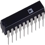
ICGOO电子元器件商城为您提供AD7302BNZ由Analog设计生产,在icgoo商城现货销售,并且可以通过原厂、代理商等渠道进行代购。 AD7302BNZ价格参考¥42.08-¥70.89。AnalogAD7302BNZ封装/规格:数据采集 - 数模转换器, 8 位 数模转换器 2 20-PDIP。您可以下载AD7302BNZ参考资料、Datasheet数据手册功能说明书,资料中有AD7302BNZ 详细功能的应用电路图电压和使用方法及教程。
AD7302BNZ 是由 Analog Devices Inc.(ADI)生产的一款数据采集领域的数模转换器(DAC)。它属于 AD730x 系列,是一款双通道、8 位电压输出 DAC,采用 16 引脚 SOIC 封装。以下是其主要应用场景:

 1. 工业自动化与控制
   - 在工业自动化系统中,AD7302BNZ 可用于生成精确的模拟信号来控制电机、阀门或其他执行器。
   - 它可以作为 PID 控制器的一部分,将数字控制算法的输出转换为模拟电压信号,实现对温度、压力或流量等参数的精确调节。

 2. 仪器仪表
   - 该芯片适用于各种测试和测量设备,例如信号发生器或校准设备。
   - 它能够提供高精度的模拟输出,用于模拟实际信号波形,帮助验证传感器或电路的功能。

 3. 通信系统
   - 在通信领域,AD7302BNZ 可用于生成调制信号或偏置电压。
   - 它可用于射频(RF)前端的功率放大器偏置控制,确保放大器在最佳工作点运行。

 4. 消费电子
   - AD7302BNZ 的小型封装和低功耗特性使其适合便携式设备,如音频设备中的音量控制或均衡器设置。
   - 它还可以用于家用电器的控制面板,将数字输入转换为模拟输出以驱动显示屏或指示灯。

 5. 医疗设备
   - 在医疗领域,AD7302BNZ 可用于生成刺激信号,例如在心电图(ECG)或脑电图(EEG)设备中。
   - 它也可用于超声波设备中的波束形成或偏置控制。

 6. 汽车电子
   - 该芯片可用于汽车传感器接口或控制系统中,将数字信号转换为模拟信号以驱动传感器或执行器。
   - 它还可用于车内娱乐系统的音量调节或音频处理。

 特性总结
- 双通道设计:支持同时控制两个独立的模拟输出。
- 8 位分辨率:提供 256 个离散输出电平,适用于大多数中低精度应用。
- 单电源供电:兼容 5V 或 3V 系统,简化设计。
- 小型封装:SOIC 封装节省空间,适合紧凑型设计。

综上所述,AD7302BNZ 广泛应用于需要将数字信号转换为模拟信号的各种场景,特别是在对成本和尺寸敏感的应用中表现出色。
| 参数 | 数值 |
| 产品目录 | 集成电路 (IC)半导体 |
| 描述 | IC DAC 8BIT DUAL R-R 20-DIP数模转换器- DAC 2.7-5.5V Parallel Input Dual VOut 8B |
| 产品分类 | |
| 品牌 | Analog Devices Inc |
| 产品手册 | |
| 产品图片 |
|
| rohs | 符合RoHS无铅 / 符合限制有害物质指令(RoHS)规范要求 |
| 产品系列 | 数据转换器IC,数模转换器- DAC,Analog Devices AD7302BNZ- |
| 数据手册 | |
| 产品型号 | AD7302BNZ |
| 产品培训模块 | http://www.digikey.cn/PTM/IndividualPTM.page?site=cn&lang=zhs&ptm=19145http://www.digikey.cn/PTM/IndividualPTM.page?site=cn&lang=zhs&ptm=18614http://www.digikey.cn/PTM/IndividualPTM.page?site=cn&lang=zhs&ptm=26125http://www.digikey.cn/PTM/IndividualPTM.page?site=cn&lang=zhs&ptm=26140http://www.digikey.cn/PTM/IndividualPTM.page?site=cn&lang=zhs&ptm=26150http://www.digikey.cn/PTM/IndividualPTM.page?site=cn&lang=zhs&ptm=26147 |
| 产品目录页面 | |
| 产品种类 | 数模转换器- DAC |
| 位数 | 8 |
| 供应商器件封装 | 20-PDIP |
| 分辨率 | 8 bit |
| 包装 | 管件 |
| 商标 | Analog Devices |
| 安装类型 | 通孔 |
| 安装风格 | Through Hole |
| 封装 | Tube |
| 封装/外壳 | 20-DIP(0.300",7.62mm) |
| 封装/箱体 | PDIP-20 |
| 工作温度 | -40°C ~ 105°C |
| 工厂包装数量 | 18 |
| 建立时间 | 2µs |
| 接口类型 | Parallel |
| 数据接口 | 并联 |
| 最大功率耗散 | 24.8 mW |
| 最大工作温度 | + 105 C |
| 最小工作温度 | - 40 C |
| 标准包装 | 18 |
| 电压参考 | Internal, External |
| 电压源 | 单电源 |
| 电源电压-最大 | 5.5 V |
| 电源电压-最小 | 2.7 V |
| 积分非线性 | +/- 1 LSB |
| 稳定时间 | 1.2 us |
| 系列 | AD7302 |
| 转换器数 | 2 |
| 转换器数量 | 2 |
| 输出数和类型 | 2 电压,单极 |
| 输出类型 | Voltage |
| 采样比 | 833 kSPs |
| 采样率(每秒) | - |


- 商务部:美国ITC正式对集成电路等产品启动337调查
- 曝三星4nm工艺存在良率问题 高通将骁龙8 Gen1或转产台积电
- 太阳诱电将投资9.5亿元在常州建新厂生产MLCC 预计2023年完工
- 英特尔发布欧洲新工厂建设计划 深化IDM 2.0 战略
- 台积电先进制程称霸业界 有大客户加持明年业绩稳了
- 达到5530亿美元!SIA预计今年全球半导体销售额将创下新高
- 英特尔拟将自动驾驶子公司Mobileye上市 估值或超500亿美元
- 三星加码芯片和SET,合并消费电子和移动部门,撤换高东真等 CEO
- 三星电子宣布重大人事变动 还合并消费电子和移动部门
- 海关总署:前11个月进口集成电路产品价值2.52万亿元 增长14.8%


PDF Datasheet 数据手册内容提取
a 2.7 V to 5.5 V, Parallel Input Dual Voltage Output 8-Bit DAC AD7302 FEATURES FUNCTIONAL BLOCK DIAGRAM Two 8-Bit DACs In One Package 20-Lead DIP/SOIC/TSSOP Package AD7302 +2.7 V to +5.5 V Operation Internal and External Reference Capability INPUT DAC REGISTER REGISTER I DAC A I/V VOUTA DAC Power-Down Function Parallel Interface On-Chip Output Buffer DD70 REINGPISUTTER REGDIASCTER I DAC B I/V VOUTB Rail-to-Rail Operation Low Power Operation 3 mA max @ 3.3 V A/B MUX POWER ON Power-Down to 1 (cid:109)A max @ 25(cid:56)C WR COLONTGRICOL RESET APPLICATIONS CS ‚ 2 AGND Portable Battery Powered Instruments Digital Gain and Offset Adjustment PD CLR LDAC REFIN VDD DGND Programmable Voltage and Current Sources Programmable Attenuators GENERAL DESCRIPTION PRODUCT HIGHLIGHTS The AD7302 is a dual, 8-bit voltage out DAC that operates 1.␣Low Power, Single Supply Operation. This part operates from a single +2.7 V to +5.5 V supply. Its on-chip precision from a single +2.7 V to +5.5 V supply and typically consumes output buffers allow the DAC outputs to swing rail to rail. The 15mW at 5 V, making it ideal for battery powered applications. AD7302 has a parallel microprocessor and DSP-compatible 2.␣The on-chip output buffer amplifiers allow the outputs of the interface with high speed registers and double buffered interface DACs to swing rail to rail with a settling time of typically 1.2m s. logic. Data is loaded to the registers on the rising edge of CS or 3.␣Internal or external reference capability. WR and the A/B pin selects either DAC A or DAC B. 4.␣High speed parallel interface. Reference selection for AD7302 can be either an internal reference derived from the V or an external reference applied 5. Power-Down Capability. When powered down the DAC DD at the REFIN pin. Both DACs can be simultaneously updated consumes less than 1 m A at 25(cid:176) C. using the asynchronous LDAC input and can be cleared by 6. Packaged in 20-lead DIP, SOIC and TSSOP packages. using the asynchronous CLR input. The low power consumption of this part makes it ideally suited to portable battery operated equipment. The power consump- tion is less than 10 mW at 3.3 V, reducing to 3 m W in power- down mode. The AD7302 is available in a 20-pin plastic dual-in-line package, 20-lead SOIC and a 20-lead TSSOP package. REV.0 Information furnished by Analog Devices is believed to be accurate and reliable. However, no responsibility is assumed by Analog Devices for its use, nor for any infringements of patents or other rights of third parties One Technology Way, P.O. Box 9106, Norwood, MA 02062-9106, U.S.A. which may result from its use. No license is granted by implication or Tel: 617/329-4700 World Wide Web Site: http://www.analog.com otherwise under any patent or patent rights of Analog Devices. Fax: 617/326-8703 © Analog Devices, Inc., 1997
AD7302–SPECIFICATIONS (V = +2.7 V to +5.5 V, Internal Reference; C = 100 pF, R = 10 k(cid:86) to V and GND; DD L L DD to T unless otherwise noted) MAX Parameter B Versions1 Units Conditions/Comments STATIC PERFORMANCE Resolution 8 Bits Relative Accuracy – 1 LSB max Note 2 Differential Nonlinearity – 1 LSB max Guaranteed Monotonic Full-Scale Error –0.75 LSB typ Zero Code Error @ 25(cid:176) C 3 LSB typ All Zeroes Loaded to DAC Register Gain Error3 – 1 % FSR typ Zero Code Temperature Coefficient 100 m V/(cid:176) C typ DAC REFERENCE INPUT REFIN Input Range 1.0 to V /2 V min to max DD REFIN Input Impedance 10 MW typ OUTPUT CHARACTERISTICS Output Voltage Range 0 to V V min to max DD Output Voltage Settling Time 2 m s max Typically 1.2 m s Slew Rate 7.5 V/m s typ Digital to Analog Glitch Impulse 1 nV-s typ 1 LSB Change Around Major Carry Digital Feedthrough 0.2 nV-s typ Digital Crosstalk 0.2 nV-s typ Analog Crosstalk – 0.2 LSB typ DC Output Impedance 40 W typ Short Circuit Current 14 mA typ Power Supply Rejection Ratio4 0.0003 %/% max D V = – 10% DD LOGIC INPUTS Input Current – 10 m A max V , Input Low Voltage 0.8 V max V = +5 V INL DD V , Input Low Voltage 0.6 V max V = +3␣V INL DD V , Input High Voltage 2.4 V min V = +5 V INH DD V , Input High Voltage 2.1 V min V = +3 V INH DD Pin Capacitance 7 pF max POWER REQUIREMENTS V 2.7/5.5 V min/max DD I Both DACs Active and Excluding Load Currents DD V = 3.3 V V = V and V = GND DD IH DD IL @ 25(cid:176) C 2.8 mA max Typically 2.3 mA @ T to T 3 mA max See Figures 6 and 7 MIN MAX V = 5.5 V V = V and V = GND DD IH DD IL @ 25(cid:176) C 4.5 mA max Typically 2.8 mA @ T to T 5 mA max See Figures 6 and 7 MIN MAX I (Full Power-Down) DD @ 25(cid:176) C 1 m A max V = V and V = GND IH DD IL T to T 2 m A max See Figure 18 MIN MAX NOTES 1Temperature ranges are as follows: B Version: –40(cid:176) C to +105(cid:176)C. 2Relative Accuracy is calculated using a reduced code range of 15 to 245. 3Gain error is specified between Codes 15 and 245. The actual error at Code 15 is typically 3 LSB. 4Guaranteed by characterization at product release, not production tested. Specifications subject to change without notice. –2– REV. 0
AD7302 TIMING CHARACTERISTICS1, 2 (VDD = +2.7 V to +5.5 V; GND = 0 V; Reference = Internal VDD/2 Reference; all specifications T to T unless otherwise noted) MIN MAX Limit at T , T MIN MAX Parameter (B Version) Units Conditions/Comments t 0 ns min Address to Write Setup Time 1 t 0 ns min Address Valid to Write Hold Time 2 t 0 ns min Chip Select to Write Setup Time 3 t 0 ns min Chip Select to Write Hold Time 4 t 20 ns min Write Pulse Width 5 t 15 ns min Data Setup Time 6 t 4.5 ns min Data Hold Time 7 t 20 ns min Write to LDAC Setup Time 8 t 20 ns min LDAC Pulse Width 9 t 20 ns min CLR Pulse Width 10 NOTES 1Sample tested at +25(cid:176) C to ensure compliance. All input signals are specified with tr = tf = 5 ns (10% to 90% of V ) and timed from a voltage level of DD (V + V )/2. tr and tf should not exceed 1 m s on any digital input. IL IH 2See Figure 1. t1 t2 A/B CS t3 t4 t5 WR t7 t6 D7–D0 t8 t9 LDAC t10 CLR Figure 1.Timing Diagram for Parallel Data Write REV. 0 –3–
AD7302 ABSOLUTE MAXIMUM RATINGS* TSSOP Package, Power Dissipation . . . . . . . . . . . . . 700 mW (TA = +25(cid:176) C unless otherwise noted) q JA Thermal Impedance . . . . . . . . . . . . . . . . . . . . 143(cid:176) C/W V to GND . . . . . . . . . . . . . . . . . . . . . . . . . . –0.3 V to +7 V Lead Temperature, Soldering DD Reference Input Voltage to AGND . . . .–0.3 V to V + 0.3␣V ␣␣Vapor Phase (60 sec) . . . . . . . . . . . . . . . . . . . . . . .+215(cid:176) C DD Digital Input Voltage to DGND . . . . . –0.3 V to V + 0.3 V ␣␣Infrared (15 sec) . . . . . . . . . . . . . . . . . . . . . . . . . .+220(cid:176) C DD AGND to DGND . . . . . . . . . . . . . . . . . . . . . . . –0.3 V, 0.3 V SOIC Package, Power Dissipation . . . . . . . . . . . . . . . 870 mW V A, V B to AGND . . . . . . . . . . . .–0.3 V, V + 0.3 V q Thermal Impedance . . . . . . . . . . . . . . . . . . . . . 74(cid:176) C/W OUT OUT DD JA Operating Temperature Range Lead Temperature, Soldering Commercial (B Version) . . . . . . . . . . . . . –40(cid:176) C to +105(cid:176) C ␣␣Vapor Phase (60 sec) . . . . . . . . . . . . . . . . . . . . . . .+215(cid:176) C Storage Temperature Range . . . . . . . . . . . . –65(cid:176) C to +150(cid:176) C ␣␣Infrared (15 sec) . . . . . . . . . . . . . . . . . . . . . . . . . .+220(cid:176) C Junction Temperature . . . . . . . . . . . . . . . . . . . . . . . . .+150(cid:176) C *Stresses above those listed under Absolute Maximum Ratings may cause perma- Plastic DIP Package, Power Dissipation . . . . . . . . . . 900 mW nent damage to the device. This is a stress rating only; functional operation of the q Thermal Impedance . . . . . . . . . . . . . . . . . . . . 102(cid:176) C/W device at these or any other conditions above those listed in the operational JA Lead Temperature (Soldering, 10 sec) . . . . . . . . . . .+260(cid:176) C sections of this specification is not implied. Exposure to absolute maximum rating conditions for extended periods may affect device reliability. CAUTION ESD (electrostatic discharge) sensitive device. Electrostatic charges as high as 4000 V readily WARNING! accumulate on the human body and test equipment and can discharge without detection. Although the AD7302 features proprietary ESD protection circuitry, permanent damage may occur on devices subjected to high energy electrostatic discharges. Therefore, proper ESD precautions are recommended to avoid performance degradation or loss of functionality. ESD SENSITIVE DEVICE ORDERING GUIDE Temperature Package Model Range Options* AD7302BN –40(cid:176) C to +105(cid:176) C N-20 AD7302BR –40(cid:176) C to +105(cid:176) C R-20 AD7302BRU –40(cid:176) C to +105(cid:176) C RU-20 *N = Plastic DIP; R = Small Outline; RU =Thin Shrink Small Outline. –4– REV. 0
AD7302 PIN FUNCTION DESCRIPTIONS Pin No. Mnemonic Function 1-8 D7–D0 Parallel Data Inputs. Eight-bit data is loaded to the input register of the AD7302 under the control of CS and WR. 9 CS Chip Select. Active low logic input. 10 WR Write Input. WR is an active low logic input used in conjunction with CS and A/B to write data to the selected DAC register. 11 A/B DAC Select. Address pin used to select writing to either DAC A or DAC B. 12 PD Active low input used to put the part into low power mode reducing current consumption to less than 1 m A. 13 LDAC Load DAC Logic Input. When this logic input is taken low both DAC outputs are simultaneously updated with the contents of their DAC registers. If LDAC is permanently tied low, the DACs are updated on the rising edge of WR. 14 CLR Asynchronous Clear Input (Active Low). When this input is taken low the DAC registers are loaded with all zeroes and the DAC outputs are cleared to zero volts. 15 V Power Supply Input. These parts can be operated from 2.7 V to 5.5 V and should be decoupled to AGND. DD 16 REFIN External Reference Input. This can used as the reference for both DACs. The range on this reference input is 1 V to V /2. If REFIN is directly tied to V the internal V /2 reference is selected. DD DD DD 17 AGND Analog Ground reference point and return point for all analog current on the part. 18 V B Analog output voltage from DAC B. The output amplifier can swing rail to rail on its output. OUT 19 V A Analog output voltage from DAC A. The output amplifier can swing rail to rail on its output. OUT 20 DGND Digital Ground reference point and return point for all digital current on the part. PIN CONFIGURATION (MSB) DB7 1 20 DGND DB6 2 19 VOUTA DB5 3 18 VOUTB DB4 4 17 AGND DB3 5 AD7302 16 REFIN DB2 6 (NToOt Pto V SIEcaWle) 15 VDD DB1 7 14 CLR (LSB) DB0 8 13 LDAC CS 9 12 PD WR 10 11 A/B REV. 0 –5–
AD7302 TERMINOLOGY DIGITAL FEEDTHROUGH INTEGRAL NONLINEARITY Digital Feedthrough is a measure of the impulse injected into For the DACs, relative accuracy or endpoint nonlinearity is a the analog output of a DAC from the digital inputs of the same measure of the maximum deviation, in LSBs, from a straight DAC, but is measured when the DAC is not updated. It is specified in nV-s and measured with a full-scale code change on line passing through the endpoints of the DAC transfer function. the data bus, i.e., from all 0s to all 1s and vice versa. A graphical representation of the transfer curve is shown in Figure 14. DIGITAL CROSSTALK Digital Crosstalk is the glitch impulse transferred to the output DIFFERENTIAL NONLINEARITY of one converter due to a digital code change to another DAC. Differential Nonlinearity is the difference between the measured It is specified in nV-s. change and the ideal 1 LSB change between any two adjacent codes. A specified differential nonlinearity of – 1 LSB maximum ANALOG CROSSTALK ensures monotonicity. Analog Crosstalk is a change in output of any DAC in response to a change in the output of the other DAC. It is measured in ZERO CODE ERROR LSBs. Zero Code Error is the measured output voltage from V of OUT either DAC when zero code (all zeros) is loaded to the DAC POWER SUPPLY REJECTION RATIO (PSRR) latch. It is due to a combination of the offset errors in the DAC This specification indicates how the output of the DAC is and output amplifier. Zero scale error is expressed in LSBs. affected by changes in the power supply voltage. Power supply rejection ratio is quoted in terms of % change in output per % GAIN ERROR change in V for full-scale output of the DAC. V is varied DD DD This is a measure of the span error of the DAC. It is the deviation – 10%. in slope of the DAC transfer characteristic from ideal, expressed as a percent of the full-scale value. It includes full-scale errors but not offset errors. DIGITAL-TO-ANALOG GLITCH IMPULSE Digital-to-Analog Glitch Impulse is the impulse injected into the analog output when the digital inputs change state with the DAC selected and the LDAC used to update the DAC. It is normally specified as the area of the glitch in nV-s and is measured when the digital input code is changed by 1 LSB at the major carry transition. –6– REV. 0
Typical Performance Characteristics–AD7302 800 5 3.5 720 VDD = 5V AND 3V 4.92 3.25 INTERNAL REFERENCE 640 TA = +25C 4.84 3.0 DAC LOADED WITH 00HEX 560 4.76 2.75 V – mVOUT 434028000 –VoltsUT 444..65.682 – VoltsOUT 222.2..505 240 VO4.44 VINDTDE =R 5NVAL REFERENCE V1.75 IVNDTDE =R N3VAL REFERENCE 16800 44..3268 D T WAA =CIT +HR2 EF5G(cid:176)FCIHSETXER LOADED 11.2.55 D T WAA C=IT +HR2 EF5GF(cid:176)CIHSeTxER LOADED 0 4.2 1.0 0 2 4 6 8 0 2 4 6 8 0 1 2 3 4 5 6 7 8 SINK CURRENT – mA SOURCE CURRENT – mA SOURCE CURRENT – mA ␣Figure 2.Output Sink Current Capa- Figure 3.Output Source Current Figure 4.Output Source Current ␣bility with VDD = 3 V and VDD = 5 V Capability with VDD = 5 V Capability with VDD = 3 V 0.5 5.0 7.0 BOTH DACS ACTIVE 00.4.45 VTAD D= =+ 255V(cid:56)C 44..50 6.0 I TNAT E=R +N2A5(cid:176)LC REFERENCE USED 0.35 3.5 VDD = 5.5V 5.0 ERROR – LSBs 000.2..235 INL ERROR I – mADD 232...005 VDD = 3.3V I – mADD34..00 LOGIC INPUTS = VIH OR VIL 0.15 1.5 DNL ERROR INTERNAL REFERENCE 0.1 1.0 LOGIC INPUTS = VDD OR GND 2.0 0.05 0.5 BOTH DACS ACTIVE LOGIC INPUTS = VDD OR GND 0 0 1.0 1.0 1.2 1.4 1.6 1.8 2.0 2.2 2.4 2.6 2.8 –50 –25 0 25 50 75 100 125 2.5 3.0 3.5 4.0 4.5 5.0 5.5 REFERENCE VOLTAGE – Volts TEMPERATURE – C VDD – Volts ␣␣␣␣Figure 5.Relative Accuracy vs. Figure 6.Typical Supply Current Figure 7.Typical Supply Current ␣␣␣␣External Reference vs. Temperature vs. Supply Voltage 10 5 WR T 0 1 ‹ –5 PD B N – d–10 2 ‹ 2 O–15 UATI–20 VOUT VOUT ‹ N E ATT––2350 VEXDDT E=R 5NVAL SINEWAVE REFERENCE I VN RDTDEE F=RE 3NRVAELN VCOELTAGE 1 AVDOU7T302 POWER-UP TIME –35 DTAA C= +R2E5G(cid:176)CISTER LOADED WITH FFHEX 3 ‹ F CUHLLA NSGCAE L0E0 HC-OFFDHE VINDTDE =R N5VAL REFERENCE –40 TA = +25(cid:176)C DAC IN POWER-DOWN INITIALLY 1 10 100 1k 10k FREQUENCY – Hz CH1 5V, CH2 1V, CH3 20mV CH1 = 2V/div, CH2 = 5V/Div, TIME BASE = 200 ns/Div TIME BASE = 2 µs/Div ␣␣␣␣␣␣Figure 8.Large Scale Signal Figure 9.Full-Scale Settling Time ␣Figure 10.Exiting Power-Down (Full ␣␣␣␣␣␣Frequency Response ␣Power-Down) REV. 0 –7–
AD7302 10 1 T VDD LSB 789 VDINDATDCE = RL N2O.AA7 LDT EORDE 5 F.W5EVIRTEHN ACLEL ZEROES 1 ‹ WR VI N RDTDEE F=RE 5NRVAELN VCOELTAGE 2 T RROR – 65 1TA0 =L S+B25 S(cid:56)CTEP CHANGE VOA DE E 4 VOUT O DAC B 3 T O C 3 VOB ER 2 DAC A Z 1 2 ‹ 0 CH1 5.00V CH2 5.00V M20.0ms CH1 –50 –25 0 25 50 75 100 125 CH1 5.00V, CH2 50.0mV, M 250ns CH3 5.00V TEMPERATURE – C Figure 11.Power-On—RESET Figure 12.Zero Code Error vs. Figure 13.Small-Scale Settling Time Temperature 00..45 VINDTDE =R 5NVAL REFERENCE 00..54 00..54 5kW 100pf. LOAD 0.3 LIMITED CODE RANGE (10–245) 0.3 0.3 B 0.2 TA = +25(cid:176)C B 0.2 VDD = 5V B 0.2 ROR – LS 0.01 DAC A ROR – LS 0.01 INTERNAL REFERENCE ROR – LS 0.01 VINDTDE =R N5VAL REFERENCE L ER–0.1 DAC B L ER–0.1 L ER–0.1 IN–0.2 IN–0.2 DN–0.2 –0.3 –0.3 –0.3 –0.4 –0.4 –0.4 –0.50 32 64 96 128 160 192 224 256 –0.5–60–40–20 0 20 40 60 80 100120140 –0.5–60–40–20 0 20 40 60 80 100120140 INPUT CODE (10 to 245) TEMPERATURE – (cid:56)C TEMPERATURE – (cid:56)C Figure 14.Integral Linearity Plot Figure 15.Typical INL vs. Temperature Figure 16.Typical DNL vs. Temperature 1.0 1000 (cid:54)R – % 0.8 VDD = 5V NT – nA 789000000 VLODDG =IC 5 IVNPUTS = VDD OR GND O E RENCE ERR 00..64 DOWN CURR 456000000 T REFE 0.2 POWER- 230000 N I 100 0 0 –50 –25 0 25 50 75 100 125 –60–40–20 0 20 40 60 80 100120140 TEMPERATURE – C TEMPERATURE – (cid:56)C Figure 17.Typical Internal Reference Figure 18. Power-Down Current vs. Error vs. Temperature Temperature –8– REV. 0
AD7302 GENERAL DESCRIPTION The internal reference is selected by tying the REFIN pin to D/A Section V . If an external reference is to be used, this can be directly DD The AD7302 is a dual 8-bit voltage output digital-to-analog applied to the REFIN pin; if this is 1 V below V , the internal DD converter. The architecture consists of a reference amplifier, a circuitry will select this externally applied reference as the current source DAC followed by a current-to-voltage converter reference source for the DAC. capable of generating rail-to-rail voltages on the output of the Digital Interface DAC. Figure 19 shows a block diagram of the basic DAC The AD7302 contains a fast parallel interface allowing this dual architecture. DAC to interface to industry standard microprocessors, micro- controllers and DSP machines. There are two modes in which AD7302 this parallel interface can be configured to update the DAC VDD REFERENCE outputs. The simultaneous update mode allows simultaneous AMPLIFIER 11.7kW 30kW updating of both DAC outputs. The automatic update mode + CURRENT allows each DAC to be individually updated following a write REFIN - DAC11.7kW I/V VO A/B cycle. Figure 21 shows the internal logic associated with the 30kW digital interface. The PON STRB signal is internally generated from the power on reset circuitry and is low during the power- on reset phase of the power-up procedure. Figure 19.DAC Architecture CLR Both DAC A and DAC B outputs are internally buffered and CLR these output buffer amplifiers have rail-to-rail output character- PON STRB istics. The output amplifier is capable driving a load of 10 kW to CLEAR MLE A rbeoftehr eVnDceD saenledc gtiroonu nfodr itnh ep aDraAlCle lc wanit hei tah 1er0 b0ep iFn tteor ngarlolyu ngedn. eTrahteed LDAC SLEDTA SCLE CODLONATGCR IACOL DAC A SEL SLE A from V or externally applied through the REFIN pin. A DD ENABLE comparator on the REFIN pin detects whether the required reference is the internally generated reference or the externally A/B CLEAR MLE B applied voltage to the REFIN pin. If REFIN is connected to SET SLE DAC B CONTROL V , the reference selected is the internally generated V /2 LDAC LOGIC reDfeDrence. When an externally applied voltage is more thDaDn one DAC B SEL SLE B CS ENABLE volt below V , the comparator selection switches to the DD WR externally applied voltage to the REFIN pin. The range on the Figure 21.Logic Interface external reference input is from 1.0 V to V /2. The output DD voltage from either DAC is given by: The AD7302 has a double buffered interface, which allows V A/B = 2 · V · (N/256) for simultaneous updating of the DAC outputs. Figure 22 shows O REF where: a block diagram of the register arrangement within the AD7302. V is the voltage applied to the external REFIN pin or REF V /2 when the internal reference is selected. DB7–DB0 DD ␣␣ N is the decimal equivalent of the code loaded to the DAC INPUT register and ranges from 0 to 255. REGISTER 8 Reference 4 4 The AD7302 has the facility to use either an external reference 4 TO 15 4 TO 15 applied through the REFIN pin or an internal reference DECODER DECODER generated from VDD. Figure 20 shows the reference input 15 15 eaxrrtaenrngaelmlye anpt pwliheedr er eefietrheenrc teh cea inn tbeer nsaell eVcDteDd/2. reference or the MLE SLE REGDIASCTER REGDIASCTER A/B 15 15 CS CONTROL VDD LDWACR LOGIC DRIVERS DRIVERS VTH CLR 30 30 PMOS COMPARATOR INT REF LOWER UPPER REFIN NIBBLE NIBBLE Figure 22.Register Arrangement EXT REF INT MUX REF SELECTED REFERENCE OUTPUT Figure 20.Reference Selection Circuitry REV. 0 –9–
AD7302 Automatic Update Mode POWER-ON RESET In this mode of operation the LDAC signal is permanently tied The AD7302 has a power-on reset circuit designed to allow low. The state of the LDAC is sampled on the rising edge of output stability during power-up. This circuit holds the DACs WR. LDAC being low allows the selected DAC register to be in a reset state until a write takes place to the DAC. In the reset automatically updated on the rising edge of WR. The output state all zeros are latched into the input registers of each DAC update occurs on the rising edge of WR. Figure 23 shows the and the DAC registers are in transparent mode, thus the output timing associated with the automatic update mode of operation of both DACs is held at ground potential until a write takes and also the status of the various registers during this frame. place to the DAC. The power-on reset circuitry generates a PON STRB signal, which is a gating signal used within the logic to identify a power-on condition. A/B POWER-DOWN FEATURES CS The AD7302 has a power-down feature. This is implemented by exercising the external PD pin; an active low signal puts the WR complete DAC into power-down mode. When in power-down D7–D0 the current consumption of the device is reduced to 1 m A max at 25(cid:176) C and 2 m A max over temperature, making the device LDAC = 0 suitable for use in portable battery powered equipment. When I/P REG (MLE) HOLD TRACK HOLD power-down is activated, the reference bias servo loop and the output amplifiers with their associated linear circuitry are DAC REG (SLE) TRACK HOLD TRACK powered down, the reference resistors are open circuited to further reduce the power consumption. The output sees a load VOUT of approximately 23 kW to GND when in power-down mode as shown in Figure 25. The contents of the data registers are Figure 23.Timing and Register Arrangement for Auto- unaffected when in power-down mode. The device comes out matic Update Mode of power-down in typically 13 m s (see Figure 10). Simultaneous Update Mode In this mode of operation the LDAC signal is used to update both 11.7kW DAC outputs simultaneously. The state of the LDAC is sampled VDD on the rising edge of WR. If LDAC is high, the automatic update mode is disabled and both DAC latches are updated at any time IDAC after the write by taking LDAC low. The output update occurs 11.7kW on the falling edge of LDAC. LDAC must be taken back high VREF again before the next data transfer takes place. Figure 24 shows the timing associated with the simultaneous update mode of operation and also the status of the various registers during this frame. Figure 25.Output Stage During Power-Down Analog Outputs A/B The AD7302 contains two independent voltage output DACs with 8-bit resolution and rail-to-rail operation. The output buffer CS provides a gain of two at the output. Figures 2 to 4 show the source and sink capabilities of the output amplifier. The slew WR rate of the output amplifier is typically 7.5 V/m s and has a full- scale settling to 8 bits with a 100 pF capacitive load in typically D7–D0 1.2 m s. LDAC The input coding to the DAC is straight binary. Table I shows the binary transfer function for the AD7302. Figure 26 shows I/P REG (MLE) HOLD TRACK HOLD the DAC transfer function for binary coding. Any DAC output voltage can be expressed as: DAC REG (SLE) HOLD TRACK HOLD V = 2 · V (N/256) OUT REF where: VOUT ␣␣N is the decimal equivalent of the binary input code. Figure 24.Timing and Register Arrangement for Simulta- N ranges from 0 to 255. neous Update Mode –10– REV. 0
AD7302 ␣␣V is the voltage applied to the external REFIN pin when REF VDD = 3 TO 5V the external reference is selected and is V /2 if the DD 0.1µF 10µF internal reference is used. Table I. Output Voltage for Selected Input Codes Digital Input VDD AGNDDGND VOUTA VOUTA MSB . . . LSB Analog Output REF IN 1111 1111 2 · 255/256 · V V AD7302 REF 1111 1110 2 · 254/256 · VREF V CPDLR VOUTB VOUTB 1000 0001 2 · 129/256 · VREF V D7–D0 A/B CS WR LDAC 1000 0000 VREF V VDD 0111 1111 2 · 127/256 · V V REF 0000 0001 2 · V /256␣V DATA BUS CONTROL INPUTS REF 0000 0000 0 V Figure 27.Typical Configuration Selecting the Internal Reference Figure 28 shows a typical setup for the AD7302 when using an 2.VREF external reference. The reference range for the AD7302 is from 1 V to V /2 V. Higher values of reference can be incorporated, DD but will saturate the output at both the top and bottom end of E G the transfer function. There is a gain of two from input to output A LT on the AD7302. Suitable references for 5 V operation are the O UT V VREF AD780 and REF192. For 3 V operation a suitable external P reference would be the AD589 a 1.23 V bandgap reference. T U O C DA VDD = 3 TO 5V 0.1µF 10µF 0 DACCO INDPEUT 00 01 7F 80 81 FE FF VIN VDD AGNDVDOGUNTAD VOUTA EXT REF VOUT REF IN 0.1µF AD7302 Figure 26.DAC Transfer Function GND CLR Figure 27 shows a typical setup for the AD7302 when using its PD VOUTB VOUTB internal reference. The internal reference is selected by tying the AD780/REF192 D7–D0 A/B CS WR LDAC REFIN pin to V . Internally in the reference section there is a WITH OVDRD = 5V VDD DD AD589 WITH VDD = 3V reference detect circuit that will select the internal V /2 based DD DATA BUS CONTROL INPUTS on the voltage connected to the REFIN pin. If REFIN is within a threshold voltage of a PMOS device (approximately 1 V) of Figure 28.Typical Configuration Using An External V the internal reference is selected. When the REFIN voltage Reference DD is more than 1 V below V , the externally applied voltage at DD this pin is used as the reference for the DAC. The internal reference on the AD7302 is V /2, the output current to voltage DD converter within the AD7302 provides a gain of two. Thus the output range of the DAC is from 0 V to V , based on Table I. DD REV. 0 –11–
AD7302 MICROPROCESSOR INTERFACING AD7302–ADSP-2101/ADSP-2103 Interface A15 ADDRESS BUS Figure 29 shows an interface between the AD7302 and the A0 ADSP-2101/ADSP-2103. The fast interface timing associated A** with the AD7302 allows easy interface to the ADSP-2101/ A/B IS EN ADDR ADSP-2103. DECODE CS AD7302* TMS32020 A+1** LDAC STRB DMA14 WR R/W ADDRESS BUS DMA0 DB7 A** DB0 A/B DMS EN ADDR DECODE CS DMD15 AD7302* ADSP-2101*/ DATA BUS ADSP-2103* A+1** LDAC DMD0 **ADDITIONAL CIRCUITRY OMITTED FOR CLARITY. **A DECODED ADDRESS FOR DAC A. WR WR **A+1 DECODED ADDRESS FOR DAC B. DB7 Figure 30.AD7302–TMS32020 Interface DB0 In the circuit shown the LDAC is hardwired low, thus the selected DAC output is updated on the rising edge of WR. DMD15 DATA BUS Some applications may require simultaneous updating of both DMD0 **ADDITIONAL CIRCUITRY OMITTED FOR CLARITY. DACs in the AD7302. In this case the LDAC signal can be **A DECODED ADDRESS FOR DAC A. driven from an external timer or can be controlled by the **A+1 DECODED ADDRESS FOR DAC B. microprocessor. One option for simultaneous updating is to Figure 29.AD7302–ADSP-2101/ADSP-2103 Interface decode the LDAC from the address bus so that a write opera- Two addresses are decoded to select loading data to either tion at this address will simultaneously update both DAC DAC A or DAC B. LDAC is permanently tied low in this outputs. A simple OR gate with one input driven from the circuit, so the selected DAC output is updated on the rising decoded address and the second input from the WR signal will edge of the WR signal. implement this function. Data is loaded to the AD7302 input register using the following AD7302–8051/8088 Interface ADSP-21xx instruction: Figure 31 shows a serial interface between the AD7302 and the DM (DAC) = MR0 8051/8088 processors. The address decoder is used to decode the addresses for DAC A and DAC B. MR0 = ADSP-21xx MR0 Register. DAC = Decoded DAC Address. A15 AD7302–TMS32020 Interface ADDRESS BUS A8 Figure 30 shows an interface between the AD7302 and the A** TMS32020. The address decoder is used to decode the /B addresses for DAC A and DAC B. Data is loaded to the OR ADDR DECODE AD7302 using the following instruction: AD7302* A+1** OUT DAC, D 8051/8088 DAC = Decoded DAC Address. OCTAL DB7 ALE LATCH D = Data Memory Address. DB0 AD7 ADDRESS/DATA BUS AD0 **ADDITIONAL CIRCUITRY OMITTED FOR CLARITY. **A DECODED ADDRESS FOR DAC A. **A+1 DECODED ADDRESS FOR DAC B. Figure 31.AD7302–8051//8088 Interface –12– REV. 0
AD7302 APPLICATIONS AD7302 Bipolar Operation Using the AD7302 DATA BUS VOUTA The AD7302 has been designed for single supply operation, but bipolar operation is achievable using the circuit shown in D0 VOUTB Figure 32. The circuit shown has been configured to achieve an VDD D8 output voltage range of –5 V < V < +5 V. Rail-to-rail operation O at the amplifier output is achievable using an AD820 or OP295 ENABLE 1 VCC 1Y0 AD7302 as the output amplifier. CODED 1A 1Y1 VOUTA ADDRESS 1B The output voltage for any input code can be calculated as 1Y2 follows: 74HC1391Y3 DD08 VOUTB DGND V = [(1+R4/R3) · (R2/(R1+R2) · (2 · V · D/256)] – R4 · V /R3 O REF REF AD7302 where VOUTA ␣␣D is the decimal equivalent of the code loaded to the DAC and D0 VOUTB ␣␣V is the reference voltage input. D8 REF With V = 2.5 V, R1 = R3 = 10␣kW and R2 = R4 = 20 kW and REF V = 5␣V. AD7302 DD V = (10 · D/256) – 5V VOUTA OUT D0 VOUTB VDD = 5V D8 0.1µF 10µF R4 20kW 10Rk3W +5V Figure 33.Decoding Multiple AD7302 DACs in a System – 5V AD7302 As a Digitally Programmable Window Detector AD820/ VIN VDD OP295 A digitally programmable upper/lower limit detector using the EXT REFVOUT REF IN –5V two DACs in the AD7302 is shown in Figure 34. The upper 0.1µF and lower limits for the test are loaded to DACs A and B, which GND AD7302 VOUTA in turn set the limits on the CMP04. If a signal at the V input IN is not within the programmed window an LED will indicate the R1 AD780/REF192 10kW fail condition. AGND DGND WITH VDD = 5V OR AD589 WITH VDD = 3V R202kW +5V 0.1µF 10µF VIN 1k 1k FAIL PASS Figure 32.Bipolar Operation Using the AD7302 VDD REFIN PD Decoding Multiple AD7302 in a System AD7302 The CS pin on the AD7302 can be used in applications to D7 VOUTA PASS/FAIL decode a number of DACs. In this application all DACs in the D0 system receive the same input data, but only the CS to one of A/B the DACs will be active at any one time allowing access to two CS VOUTB channels in the system. The 74HC139 is used as a two-to-four WR 1/6 74HC05 line decoder to address any of the DACs in the system. To DVDD CLR prevent timing errors from occurring, the enable input should LDAC 1/2 CMP04 DGND AGND be brought to its inactive state while the coded address inputs are changing state. Figure 33 shows a diagram of a typical setup for decoding multiple AD7302 devices in a system. The built-in power-on reset circuit on the AD7302 ensures that the outputs Figure 34.Programmable Window Detector of all DACs in the system power up with zero volts on their outputs. REV. 0 –13–
AD7302 Programmable Current Source VDD = 5V Figure 35 shows the AD7302 used as the control element of a 0.1µF 10µF programmable current source. In this circuit the full-scale R3 R4 51.2kW 390W current is set to 1 mA. The output voltage from the DAC is applied across the current setting resistor of 4.7 kW in series +5V AD820/ with the full-scale setting resistor of 470 W . Transistors suitable VIN VDD OP295 VOUT to place in the feedback loop of the amplifier include the BC107 EXT REF oa rm thine V2NSO3U9R0C4E ,o wf h6i cVh. eTnhaeb loep tehrea tcinugrr reannt gseo uisr cdee tteor mopinereadt eb yfrom GNDVOUT 0.1µF REFA IDN7302 VOUTA 39R01W the operating characteristics of the of the transistor. Suitable VOUTB amplifiers include the AD820 and the OP295 both having rail- R2 AD780/REF192 AGND DGND 51.2kW to-rail operation on their outputs. The current for any digital WITH VDD = 5V OR input code can be calculated as follows: AD589 WITH VDD = 3V I = 2 · V · D/(5E +3 · 256)mA Figure 36.Coarse/Fine Adjust Circuit REF Power Supply Bypassing and Grounding VDD = 5V In any circuit where accuracy is important, careful consideration of the power supply and ground return layout helps to ensure 0.1µF 10µF the rated performance. The printed circuit board on which the AD7302 is mounted should be designed so the analog and digital sections are separated and confined to certain areas of the VIN VDD VSOURCE board. If the AD7302 is in a system where multiple devices EXT REF require an AGND to DGND connection, the connection should VOUT REF IN +5V LOAD be made at one point only, a star ground point that should be 0.1µF GND AD7302 VOUTA established as closely as possible to the AD7302. The AD7302 AD820/ should have ample supply bypassing of 10 m F in parallel with OP295 0.1 m F on the supply located as close to the package as possible, AD780/REF192 WITH VDD = 5V AGNDDGND ideally right up against the device. The 10 m F capacitors are the 4.7kW tantalum bead type. The 0.1 m F capacitor should have low Effective Series Resistance (ESR) and Effective Series Induc- 470W tance (ESI), such as the common ceramic types, which provide a low impedance path to ground at high frequencies to handle transient currents due to internal logic switching. Figure 35.Programmable Current Source The power supply lines of the AD7302 should use as large a Coarse and Fine Adjustment Using the AD7302 trace as possible to provide low impedance paths and reduce the The DACs on the AD7302 can be paired together to form a effects of glitches on the power supply line. Fast switching sig- coarse and fine adjustment function as shown in Figure 36. In nals like clocks should be shielded with digital ground to avoid this circuit DAC A is used to provide the coarse function while radiating noise to other parts of the board and should never be DAC B is used to provide the fine adjustment. Varying the ratio run near the reference inputs. Avoid crossover of digital and of R1 and R2 will vary the relative effect of the coarse and fine analog signals. Traces on opposite sides of the board should run tune elements in the circuit. For the resistor values shown at right angles to each other. This reduces the effects of feed- DAC B has a resolution of 148 m V giving a fine tune range of through through the board. A microstrip technique is by far the approximately 2 LSBs for operation with a V of 5 V and a best, but not always possible with a double-sided board. In this DD reference of 2.5 V. The amplifiers shown allow a rail-to-rail technique, the component side of the board is dedicated to output voltage to be achieved on the output. A typical applica- ground plane while signal traces are placed on the solder side. tion for such a circuit would be in a setpoint controller. –14– REV. 0
AD7302 OUTLINE DIMENSIONS Dimensions shown in inches and (mm). 20-Lead Plastic DIP (N-20) 1.060 (26.90) 0.925 (23.50) 20 11 0.280 (7.11) 0.240 (6.10) 1 10 0.325 (8.25) 0.300 (7.62) 0.195 (4.95) PIN 1 0.060 (1.52) 0.115 (2.93) 0.210 (5.33) 0.015 (0.38) MAX 0.130 0.160 (4.06) (3.30) 0.115 (2.93) MIN 0.015 (0.381) 0.022 (0.558) 0.100 0.070 (1.77) SEATING 0.008 (0.204) 0.014 (0.356) (2.54) 0.045 (1.15) PLANE BSC 20-Lead SO (R-20) 0.5118 (13.00) 0.4961 (12.60) 20 11 1 10 0.2992 (7.60)0.2914 (7.40) 0.4193 (10.65)0.3937 (10.00) PIN 1 0.1043 (2.65) 0.0291 (0.74)x 45(cid:176) 0.0926 (2.35) 0.0098 (0.25) 8(cid:176) 0.0500 (1.27) 00..00101480 ((00..3100)) 0(B1.0.S25C70)0 00..00119328 ((00..4395)) SPELAANTIENG 00..00102951 ((00..3223)) 0(cid:176) 0.0157 (0.40) 20-Lead TSSOP (RU-20) 0.260 (6.60) 0.252 (6.40) 20 11 0.177 (4.50)0.169 (4.30) 0.256 (6.50)0.246 (6.25) 1 10 0.006 (0.15) PIN 1 0.002 (0.05) 0.0433 (1.10) MAX 8(cid:176) 0.028 (0.70) SEPALTAINNGE 0.02B56S C(0.65) 00..00101785 ((00..3109)) 0.0079 (0.20) 0(cid:176) 0.020 (0.50) 0.0035 (0.090) REV. 0 –15–
7 9 4/ – 2 1 – 0 9 9 2 C A. S. U. N D I E T N RI P –16–