ICGOO在线商城 > 集成电路(IC) > 数据采集 - 数模转换器 > TLC7226CN
 Datasheet下载
- 型号: TLC7226CN
- 制造商: Texas Instruments
- 库位|库存: xxxx|xxxx
- 要求:
| 数量阶梯 | 香港交货 | 国内含税 |
| +xxxx | $xxxx | ¥xxxx |
查看当月历史价格
查看今年历史价格
TLC7226CN产品简介:
ICGOO电子元器件商城为您提供TLC7226CN由Texas Instruments设计生产,在icgoo商城现货销售,并且可以通过原厂、代理商等渠道进行代购。 TLC7226CN价格参考¥24.54-¥50.06。Texas InstrumentsTLC7226CN封装/规格:数据采集 - 数模转换器, 8 位 数模转换器 4 20-PDIP。您可以下载TLC7226CN参考资料、Datasheet数据手册功能说明书,资料中有TLC7226CN 详细功能的应用电路图电压和使用方法及教程。
TLC7226CN 是由德州仪器 (Texas Instruments) 生产的一款数模转换器 (DAC),属于数据采集系统中的关键组件。它主要用于将数字信号转换为模拟信号,适用于多种应用场景。

 1. 工业自动化与控制
TLC7226CN 可广泛应用于工业自动化领域,特别是在需要精确控制的场景中。例如,在自动化生产线中,传感器采集到的数据通常是模拟信号,而控制系统通常使用数字信号进行处理。TLC7226CN 可以将控制系统的数字输出转换为模拟信号,用于驱动执行器、电机或阀门等设备,实现精准的闭环控制。

 2. 通信系统
在通信设备中,TLC7226CN 可用于信号调制和解调过程中。例如,在无线通信系统中,数字基带信号需要通过 DAC 转换为模拟射频信号,再通过天线发射出去。同样,在接收端,接收到的模拟信号可以通过相应的模数转换器 (ADC) 转换为数字信号进行处理。TLC7226CN 的高精度和稳定性确保了通信系统的可靠性和高效性。

 3. 音频处理
TLC7226CN 还可以应用于音频设备中,如音响、耳机放大器等。音频信号通常是模拟信号,但在现代音频处理系统中,音频信号往往以数字形式存储和传输。当需要播放音频时,DAC 将数字音频信号转换为模拟信号,驱动扬声器或耳机发出声音。TLC7226CN 的低噪声和高分辨率特性使得它能够在音频应用中提供高质量的声音输出。

 4. 医疗设备
在医疗设备中,TLC7226CN 可用于将数字信号转换为模拟信号,以驱动各种传感器或执行器。例如,在心电图机、血压计等设备中,TLC7226CN 可以将微处理器生成的数字控制信号转换为模拟信号,用于驱动显示设备或报警装置。此外,它还可以用于医学成像设备中,帮助生成精确的图像信号。

 5. 测试与测量
TLC7226CN 在测试与测量设备中也有广泛应用。例如,在示波器、信号发生器等设备中,DAC 负责将内部生成的数字波形转换为实际的模拟波形,供用户观察或测试。TLC7226CN 的高精度和快速响应特性使其成为这些设备的理想选择。

总之,TLC7226CN 凭借其出色的性能和可靠性,广泛应用于工业、通信、音频、医疗以及测试与测量等多个领域,是数据采集系统中不可或缺的关键组件。
| 参数 | 数值 |
| 产品目录 | 集成电路 (IC)半导体 |
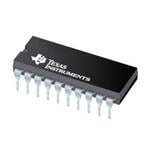
| 描述 | IC 8BIT 5US QUAD DAC P/O 20-DIP数模转换器- DAC Quad DAC 8bit |
| 产品分类 | |
| 品牌 | Texas Instruments |
| 产品手册 | |
| 产品图片 |
|
| rohs | 符合RoHS无铅 / 符合限制有害物质指令(RoHS)规范要求 |
| 产品系列 | 数据转换器IC,数模转换器- DAC,Texas Instruments TLC7226CN- |
| 数据手册 | |
| 产品型号 | TLC7226CN |
| 产品培训模块 | http://www.digikey.cn/PTM/IndividualPTM.page?site=cn&lang=zhs&ptm=13240 |
| 产品目录页面 | |
| 产品种类 | 数模转换器- DAC |
| 位数 | 8 |
| 供应商器件封装 | 20-PDIP |
| 其它名称 | 296-3018-5 |
| 分辨率 | 8 bit |
| 制造商产品页 | http://www.ti.com/general/docs/suppproductinfo.tsp?distId=10&orderablePartNumber=TLC7226CN |
| 包装 | 管件 |
| 单位重量 | 1.199 g |
| 商标 | Texas Instruments |
| 安装类型 | 通孔 |
| 安装风格 | Through Hole |
| 封装 | Tube |
| 封装/外壳 | 20-DIP(0.300",7.62mm) |
| 封装/箱体 | PDIP-20 |
| 工作温度 | 0°C ~ 70°C |
| 工厂包装数量 | 20 |
| 建立时间 | 5µs, 7µs |
| 接口类型 | Parallel |
| 数据接口 | 并联 |
| 最大工作温度 | + 70 C |
| 最小工作温度 | 0 C |
| 标准包装 | 20 |
| 电压参考 | External |
| 电压源 | 双 ± |
| 电源电压-最大 | 15.75 V |
| 电源电压-最小 | 14.25 V |
| 积分非线性 | +/- 1 LSB |
| 稳定时间 | 20 us |
| 系列 | TLC7226 |
| 结构 | R-2R |
| 转换器数 | 4 |
| 转换器数量 | 4 |
| 输出数和类型 | 4 电压,单极4 电压,双极 |
| 输出类型 | Voltage |
| 采样比 | 143 kSPs |
| 采样率(每秒) | 143k |


- 商务部:美国ITC正式对集成电路等产品启动337调查
- 曝三星4nm工艺存在良率问题 高通将骁龙8 Gen1或转产台积电
- 太阳诱电将投资9.5亿元在常州建新厂生产MLCC 预计2023年完工
- 英特尔发布欧洲新工厂建设计划 深化IDM 2.0 战略
- 台积电先进制程称霸业界 有大客户加持明年业绩稳了
- 达到5530亿美元!SIA预计今年全球半导体销售额将创下新高
- 英特尔拟将自动驾驶子公司Mobileye上市 估值或超500亿美元
- 三星加码芯片和SET,合并消费电子和移动部门,撤换高东真等 CEO
- 三星电子宣布重大人事变动 还合并消费电子和移动部门
- 海关总署:前11个月进口集成电路产品价值2.52万亿元 增长14.8%


PDF Datasheet 数据手册内容提取
(cid:25)(cid:25) (cid:1)(cid:2)(cid:3)(cid:4)(cid:5)(cid:5)(cid:6)(cid:3)(cid:7) (cid:1)(cid:2)(cid:3)(cid:4)(cid:5)(cid:5)(cid:6)(cid:8)(cid:7) (cid:1)(cid:2)(cid:3)(cid:4)(cid:5)(cid:5)(cid:6)(cid:9) (cid:10)(cid:11)(cid:12)(cid:13)(cid:14)(cid:11)(cid:15)(cid:2)(cid:16) (cid:17)(cid:18)(cid:19)(cid:8)(cid:1) (cid:13)(cid:8)(cid:20)(cid:8)(cid:1)(cid:12)(cid:2)(cid:18)(cid:1)(cid:21)(cid:18)(cid:12)(cid:22)(cid:12)(cid:2)(cid:21)(cid:20) (cid:3)(cid:21)(cid:22)(cid:23)(cid:16)(cid:14)(cid:1)(cid:16)(cid:14)(cid:24) (cid:25) SLAS060F − JANUARY 1995 − REVISED APRIL 2009 features DW OR N PACKAGE (cid:1) Four 8-Bit D/A Converters (TOP VIEW) (cid:1) Microprocessor Compatible (cid:1) TTL/CMOS Compatible OUTB 1 20 OUTC (cid:1) OUTA 2 19 OUTD Single Supply Operation Possible (cid:1) VSS 3 18 VDD CMOS Technology REF 4 17 A0 AGND 5 16 A1 applications DGND 6 15 WR (cid:1) Process Control DB7 7 14 DB0 (cid:1) DB6 8 13 DB1 Automatic Test Equipment (cid:1) DB5 9 12 DB2 Automatic Calibration of Large System DB4 10 11 DB3 Parameters, e.g. Gain/Offset description FK PACKAGE (TOP VIEW) The TLC7226C, TLC7226I, and TLC7226M consist of four 8-bit voltage-output digital-to- A B C D S T T T T analog converters (DACs) with output buffer S U U U U V O O O O amplifiers and interface logic on a single 3 2 1 20 19 monolithic chip. REF 4 18 VDD Separate on-chip latches are provided for each of AGND 5 17 A0 the four DACs. Data is transferred into one of these data latches through a common 8-bit DGND 6 16 A1 TTL/CMOS-compatible 5-V input port. Control DB7 7 15 WR inputs A0 and A1 determine which DAC is loaded DB6 8 14 DB0 when WR goes low. The control logic is speed 9 10 11 12 13 compatible with most 8-bit microprocessors. 5 4 3 2 1 B B B B B Each DAC includes an output buffer amplifier D D D D D capable of sourcing up to 5 mA of output current. The TLC7226 performance is specified for input reference voltages from 2 V to V − 4 V with dual supplies. DD The voltage mode configuration of the DACs allows the TLC7226 to be operated from a single power supply rail at a reference of 10 V. The TLC7226 is fabricated in a LinBiCMOS process that has been specifically developed to allow high-speed digital logic circuits and precision analog circuits to be integrated on the same chip. The TLC7226 has a common 8-bit data bus with individual DAC latches. This provides a versatile control architecture for simple interface to microprocessors. All latch-enable signals are level triggered. Combining four DACs, four operational amplifiers, and interface logic into either a 0.3-inch wide, 20-terminal dual-in-line IC (DIP) or a small 20-terminal small-outline IC (SOIC) allows a dramatic reduction in board space requirements and offers increased reliability in systems using multiple converters. The Leadless Ceramic Chip Carrier (LCCC) package provides for operation at military temperature range. The pinout is aimed at optimizing board layout with all of the analog inputs and outputs at one end of the package and all of the digital inputs at the other. Please be aware that an important notice concerning availability, standard warranty, and use in critical applications of TexasInstruments semiconductor products and disclaimers thereto appears at the end of this data sheet. LLiinnBBiiCCMMOOSS iiss aa ttrraaddeemmaarrkk ooff TTeexxaass IInnssttrruummeennttss.. (cid:15)(cid:14)(cid:21)(cid:13)(cid:11)(cid:3)(cid:1)(cid:8)(cid:21)(cid:22) (cid:13)(cid:12)(cid:1)(cid:12) (cid:26)(cid:27)(cid:28)(cid:29)(cid:30)(cid:31)!"(cid:26)(cid:29)(cid:27) (cid:26)# $%(cid:30)(cid:30)&(cid:27)" !# (cid:29)(cid:28) ’%()(cid:26)$!"(cid:26)(cid:29)(cid:27) *!"&+ Copyright 2009, Texas Instruments Incorporated (cid:15)(cid:30)(cid:29)*%$"# $(cid:29)(cid:27)(cid:28)(cid:29)(cid:30)(cid:31) "(cid:29) #’&$(cid:26)(cid:28)(cid:26)$!"(cid:26)(cid:29)(cid:27)# ’&(cid:30) ",& "&(cid:30)(cid:31)# (cid:29)(cid:28) (cid:1)&-!# (cid:8)(cid:27)#"(cid:30)%(cid:31)&(cid:27)"# #"!(cid:27)*!(cid:30)* .!(cid:30)(cid:30)!(cid:27)"/+ (cid:15)(cid:30)(cid:29)*%$"(cid:26)(cid:29)(cid:27) ’(cid:30)(cid:29)$&##(cid:26)(cid:27)0 *(cid:29)&# (cid:27)(cid:29)" (cid:27)&$&##!(cid:30)(cid:26))/ (cid:26)(cid:27)$)%*& "&#"(cid:26)(cid:27)0 (cid:29)(cid:28) !)) ’!(cid:30)!(cid:31)&"&(cid:30)#+ POST OFFICE BOX 655303 • DALLAS, TEXAS 75265 1
(cid:1)(cid:2)(cid:3)(cid:4)(cid:5)(cid:5)(cid:6)(cid:3)(cid:7) (cid:1)(cid:2)(cid:3)(cid:4)(cid:5)(cid:5)(cid:6)(cid:8)(cid:7) (cid:1)(cid:2)(cid:3)(cid:4)(cid:5)(cid:5)(cid:6)(cid:9) (cid:25) (cid:10)(cid:11)(cid:12)(cid:13)(cid:14)(cid:11)(cid:15)(cid:2)(cid:16) (cid:17)(cid:18)(cid:19)(cid:8)(cid:1) (cid:13)(cid:8)(cid:20)(cid:8)(cid:1)(cid:12)(cid:2)(cid:18)(cid:1)(cid:21)(cid:18)(cid:12)(cid:22)(cid:12)(cid:2)(cid:21)(cid:20) (cid:3)(cid:21)(cid:22)(cid:23)(cid:16)(cid:14)(cid:1)(cid:16)(cid:14)(cid:24) (cid:25) SLAS060F − JANUARY 1995 − REVISED APRIL 2009 description (continued) The TLC7226C is characterized for operation from 0°C to 70°C. The TLC7226I is characterized for operation from −30°C to 85°C. The TLC7226M is characterized for operation from −55°C to 125°C. AVAILABLE OPTIONS PACKAGE TA SMALL OUTLINE PLASTIC DIP LCCC (DW) (N) (FK) 0°C to 70°C TLC7226CDW TLC7226CN — −30°C to 85°C TLC7226IDW TLC7226IN — −55°C to 125°C — — TLC7226MFKB functional block diagram 4 REF _ 2 8 Latch 8 OUTA DAC A + A _ 1 8 Latch 8 OUTB DAC B + 7−14 8 B DB0−DB7 _ 20 8 Latch 8 OUTC DAC C + C _ 19 8 Latch 8 OUTD DAC D + D 15 WR 17 Control A0 Logic 16 A1 schematic of outputs EQUIVALENT ANALOG OUTPUT VDD Output 450 µA VSS 2 POST OFFICE BOX 655303 • DALLAS, TEXAS 75265
(cid:25) (cid:1)(cid:2)(cid:3)(cid:4)(cid:5)(cid:5)(cid:6)(cid:3)(cid:7) (cid:1)(cid:2)(cid:3)(cid:4)(cid:5)(cid:5)(cid:6)(cid:8)(cid:7) (cid:1)(cid:2)(cid:3)(cid:4)(cid:5)(cid:5)(cid:6)(cid:9) (cid:10)(cid:11)(cid:12)(cid:13)(cid:14)(cid:11)(cid:15)(cid:2)(cid:16) (cid:17)(cid:18)(cid:19)(cid:8)(cid:1) (cid:13)(cid:8)(cid:20)(cid:8)(cid:1)(cid:12)(cid:2)(cid:18)(cid:1)(cid:21)(cid:18)(cid:12)(cid:22)(cid:12)(cid:2)(cid:21)(cid:20) (cid:3)(cid:21)(cid:22)(cid:23)(cid:16)(cid:14)(cid:1)(cid:16)(cid:14)(cid:24) (cid:25) SLAS060F − JANUARY 1995 − REVISED APRIL 2009 Terminal Functions TERMINAL II//OO DDEESSCCRRIIPPTTIIOONN NAME NO.† AGND 5 Analog ground. AGND is the reference and return terminal for the analog signals and supply. A0, A1 17, 16 I DAC select inputs. The combination of high or low levels select either DACA, DACB, DACC, or DACD. DGND 6 Digital ground. DGND is the reference and return terminal for the digital signals and supply. DB0−DB7 14−7 I Digital DAC data inputs. DB0−DB7 are the input digital data used for conversion. OUTA 2 O DACA output. OUTA is the analog output of DACA. OUTB 1 O DACB output. OUTB is the analog output of DACB. OUTC 20 O DACC output. OUTC is the analog output of DACC. OUTD 19 O DACD output. OUTD is the analog output of DACD. REF 4 I Voltage reference input. The voltage level on REF determines the full scale analog output. VDD 18 Positive supply voltage input terminal VSS 3 Negative supply voltage input terminal WR 15 I Write input. WR selects DAC transparency or latch mode. The selected input latch is transparent when WR is low. †Terminal numbers shown are for the DW, N, and FK packages. absolute maximum ratings over operating free-air temperature range (unless otherwise noted)† Supply voltage range, V : AGND or DGND . . . . . . . . . . . . . . . . . . . . . . . . . . . . . . . . . . . . . . . . . −0.3 V to 17 V DD V ‡ . . . . . . . . . . . . . . . . . . . . . . . . . . . . . . . . . . . . . . . . . . . . . . . . . . . −0.3 V to 24 V SS Supply voltage range, V : AGND or DGND . . . . . . . . . . . . . . . . . . . . . . . . . . . . . . . . . . . . . . . . . . −7 V to 0.3 V SS Voltage range between AGND and DGND . . . . . . . . . . . . . . . . . . . . . . . . . . . . . . . . . . . . . . . . . . . . −17 V to 17 V Input voltage range, V (to DGND) . . . . . . . . . . . . . . . . . . . . . . . . . . . . . . . . . . . . . . . . . . . . −0.3 V to V + 0.3 V I DD Reference voltage range: V (to AGND) . . . . . . . . . . . . . . . . . . . . . . . . . . . . . . . . . . . . . . . . . . . −0.3 V to V ref DD V (to V ) . . . . . . . . . . . . . . . . . . . . . . . . . . . . . . . . . . . . . . . . . . . . . −0.3 V to 20 V ref SS Output voltage range, V (to AGND) (see Note 1) . . . . . . . . . . . . . . . . . . . . . . . . . . . . . . . . . . . . . . . . V to V O SS DD Continuous total power dissipation at (or below) T = 25°C (see Note 2) . . . . . . . . . . . . . . . . . . . . . . . 500 mW A Operating free-air temperature range, T : C suffix . . . . . . . . . . . . . . . . . . . . . . . . . . . . . . . . . . . . . . . 0°C to 70°C A E suffix . . . . . . . . . . . . . . . . . . . . . . . . . . . . . . . . . . . . . −30°C to 85°C M suffix . . . . . . . . . . . . . . . . . . . . . . . . . . . . . . . . . . . . −55°C to 125°C Storage temperature range, T . . . . . . . . . . . . . . . . . . . . . . . . . . . . . . . . . . . . . . . . . . . . . . . . . . . −65°C to 150°C stg Case temperature for 10 seconds: FK package . . . . . . . . . . . . . . . . . . . . . . . . . . . . . . . . . . . . . . . . . . . . . . 260°C †Stresses beyond those listed under “absolute maximum ratings” may cause permanent damage to the device. These are stress ratings only, and functional operation of the device at these or any other conditions beyond those indicated under “recommended operating conditions” is not implied. Exposure to absolute-maximum-rated conditions for extended periods may affect device reliability. ‡The VSS terminal is connected to the substrate and must be tied to the most negative supply voltage applied to the device. NOTES: 1. Output voltages may be shorted to AGND provided that the power dissipation of the package is not exceeded. Typically short circuit current to AGND is 60 mA. 2. For operation above TA = 75°C, derate linearly at the rate of 2 mW/°C. POST OFFICE BOX 655303 • DALLAS, TEXAS 75265 3
(cid:1)(cid:2)(cid:3)(cid:4)(cid:5)(cid:5)(cid:6)(cid:3)(cid:7) (cid:1)(cid:2)(cid:3)(cid:4)(cid:5)(cid:5)(cid:6)(cid:8)(cid:7) (cid:1)(cid:2)(cid:3)(cid:4)(cid:5)(cid:5)(cid:6)(cid:9) (cid:25) (cid:10)(cid:11)(cid:12)(cid:13)(cid:14)(cid:11)(cid:15)(cid:2)(cid:16) (cid:17)(cid:18)(cid:19)(cid:8)(cid:1) (cid:13)(cid:8)(cid:20)(cid:8)(cid:1)(cid:12)(cid:2)(cid:18)(cid:1)(cid:21)(cid:18)(cid:12)(cid:22)(cid:12)(cid:2)(cid:21)(cid:20) (cid:3)(cid:21)(cid:22)(cid:23)(cid:16)(cid:14)(cid:1)(cid:16)(cid:14)(cid:24) (cid:25) SLAS060F − JANUARY 1995 − REVISED APRIL 2009 recommended operating conditions MIN MAX UNIT Supply voltage, VDD 11.4 16.5 V Supply voltage, VSS −5.5 0 V High-level input voltage, VIH 2 V Low-level input voltage, VIL 0.8 V Reference voltage, Vref 0 VDD−4 V Load resistance, RL 2 kΩ Setup time, address valid before WR↓, tsu(AW) (see Figure 1) VDD = 11.4 V to 16.5 V *0 ns Setup time, data valid before WR↑, tsu(DW) (see Figure 1) VDD = 11.4 V to 16.5 V *45 ns Hold time, address valid after WR↑, th(AW) (see Figure 1) VDD = 11.4 V to 16.5 V *0 ns Hold time, data valid after WR↑, th(DW) (see Figure 1) VDD = 11.4 V to 16.5 V *10 ns Pulse duration, WR low, tw (see Figure 1) VDD = 11.4 V to 16.5 V *50 ns C suffix 0 70 OOppeerraattiinngg ffrreeee--aaiirr tteemmppeerraattuurree,, TTAA I suffix −25 85 °CC M suffix −55 125 * This parameter is not tested for M suffix devices. electrical characteristics over recommended operating free-air temperature range dual power supply over recommended power supply and reference voltage ranges, AGND = DGND = 0 V (unless otherwise noted) PARAMETER TEST CONDITIONS MIN TYP MAX UNIT II Input current, digital VI = 0 V or VDD ±1 µA VI = 0.8 V or 2.4 V, VDD = 16.5 V, I(DD) Supply current 6 16 mA VSS = − 5 V, No load I(SS) Supply current VI = 0.8 V or 2.4 V, No load 4 10 mA ri(ref) Reference input resistance 2 4 kΩ Power supply sensitivity ∆VDD = ±5% 0.01 %/% C and I suffix 65 AAllll 00ss llooaaddeedd RREEFF iinnppuutt M suffix *30 CCii IInnppuutt ccaappaacciittaannccee All 1s loaded *300 ppFF C and I suffix 8 DDiiggiittaall iinnppuuttss M suffix *12 * This parameter is not tested for M suffix devices. 4 POST OFFICE BOX 655303 • DALLAS, TEXAS 75265
(cid:25) (cid:1)(cid:2)(cid:3)(cid:4)(cid:5)(cid:5)(cid:6)(cid:3)(cid:7) (cid:1)(cid:2)(cid:3)(cid:4)(cid:5)(cid:5)(cid:6)(cid:8)(cid:7) (cid:1)(cid:2)(cid:3)(cid:4)(cid:5)(cid:5)(cid:6)(cid:9) (cid:10)(cid:11)(cid:12)(cid:13)(cid:14)(cid:11)(cid:15)(cid:2)(cid:16) (cid:17)(cid:18)(cid:19)(cid:8)(cid:1) (cid:13)(cid:8)(cid:20)(cid:8)(cid:1)(cid:12)(cid:2)(cid:18)(cid:1)(cid:21)(cid:18)(cid:12)(cid:22)(cid:12)(cid:2)(cid:21)(cid:20) (cid:3)(cid:21)(cid:22)(cid:23)(cid:16)(cid:14)(cid:1)(cid:16)(cid:14)(cid:24) (cid:25) SLAS060F − JANUARY 1995 − REVISED APRIL 2009 operating characteristics over recommended operating free-air temperature range dual power supply over recommended power supply and reference voltage ranges, AGND = DGND = 0 V (unless otherwise noted) PARAMETER TEST CONDITIONS MIN TYP MAX UNIT Slew rate *2.5 V•µs Positive full scale *5 SSeettttlliinngg ttiimmee ttoo 11//22 LLSSBB VVrreeff == 1100 VV µss Negative full scale *7 Resolution 8 bits Total unadjusted error ±2 LSB Linearity error Differential/integral ±1 LSB Full-scale error VVDDDD == 1155 VV ±±55%%,, VVrreeff == 1100 VV ±2 LSB Gain error ±0.25 LSB Full scale VDD = 14 V to 16.5 V, Vref = 10 V ±20 ppm/°C TTeemmppeerraattuurree ccooeeffffiicciieenntt ooff ggaaiinn Zero-code error ±50 µV/°C Zero-code error ±20 ±80 mV Digital crosstalk glitch impulse area Vref = 0 50 nV•s * This parameter is not tested for M suffix devices. single power supply, V = 14.25 V to 15.75 V, V = AGND = DGND = 0 V, V = 10 V (unless otherwise noted) DD SS ref PARAMETER TEST CONDITIONS MIN TYP MAX UNIT Supply current, IDD VI = 0.8 V or 2.4 V, No load 5 13 mA Slew rate *2 V•µs Positive full scale *5 SSeettttlliinngg ttiimmee ttoo 11//22 LLSSBB µss Negative full scale *20 Resolution 8 bits Total unadjusted error ±2 LSB Full-scale error ±2 LSB Full scale VDD = 14 V to 16.5 V, Vref = 10 V ±20 ppm/°C TTeemmppeerraattuurree ccooeeffffiicciieenntt ooff ggaaiinn Zero-code error ±50 µV/°C Linearity error Differential ±1 LSB Digital crosstalk-glitch impulse area 50 nV•s * This parameter is not tested for M suffix devices. POST OFFICE BOX 655303 • DALLAS, TEXAS 75265 5
(cid:1)(cid:2)(cid:3)(cid:4)(cid:5)(cid:5)(cid:6)(cid:3)(cid:7) (cid:1)(cid:2)(cid:3)(cid:4)(cid:5)(cid:5)(cid:6)(cid:8)(cid:7) (cid:1)(cid:2)(cid:3)(cid:4)(cid:5)(cid:5)(cid:6)(cid:9) (cid:25) (cid:10)(cid:11)(cid:12)(cid:13)(cid:14)(cid:11)(cid:15)(cid:2)(cid:16) (cid:17)(cid:18)(cid:19)(cid:8)(cid:1) (cid:13)(cid:8)(cid:20)(cid:8)(cid:1)(cid:12)(cid:2)(cid:18)(cid:1)(cid:21)(cid:18)(cid:12)(cid:22)(cid:12)(cid:2)(cid:21)(cid:20) (cid:3)(cid:21)(cid:22)(cid:23)(cid:16)(cid:14)(cid:1)(cid:16)(cid:14)(cid:24) (cid:25) SLAS060F − JANUARY 1995 − REVISED APRIL 2009 PARAMETER MEASUREMENT INFORMATION tsu(DW) VDD Data 0 V th(DW) VDD Address 0 V tsu(AW) th(AW) tw VDD WR 0 V NOTES: A. tr = tf = 20 ns over VDD range. B. The timing measurement reference level is equal to VIH + VIL divided by 2. C. The selected input latch is transparent while WR is low. Invalid data during this time can cause erroneous outputs. Figure 1. Write-Cycle Voltage Waveforms TYPICAL CHARACTERISTICS OUTPUT CURRENT OUTPUT CURRENT (SINK) vs vs OUTPUT VOLTAGE OUTPUT VOLTAGE 200 700 TA = 25°C 150 VDD = 15 V 600 VDD = 15 V Source Current Short-Circuit A mA 100 Limiting µ− 500 urrent − 50 nt (Sink) 400 VVSSSS = = − 05 V C 0 e put Curr 300 Out −0.1 ut − O TA = 25°C Outp 200 I −0.2 VSS = −5 V − Digital In = 0 V O I 100 −0.3 Sinking Current Source −0.4 0 −2 −1 0 1 2 0 1 2 3 4 5 6 7 8 9 10 VO − Output Voltage − V VO − Output Voltage − V Figure 2 Figure 3 6 POST OFFICE BOX 655303 • DALLAS, TEXAS 75265
(cid:25) (cid:1)(cid:2)(cid:3)(cid:4)(cid:5)(cid:5)(cid:6)(cid:3)(cid:7) (cid:1)(cid:2)(cid:3)(cid:4)(cid:5)(cid:5)(cid:6)(cid:8)(cid:7) (cid:1)(cid:2)(cid:3)(cid:4)(cid:5)(cid:5)(cid:6)(cid:9) (cid:10)(cid:11)(cid:12)(cid:13)(cid:14)(cid:11)(cid:15)(cid:2)(cid:16) (cid:17)(cid:18)(cid:19)(cid:8)(cid:1) (cid:13)(cid:8)(cid:20)(cid:8)(cid:1)(cid:12)(cid:2)(cid:18)(cid:1)(cid:21)(cid:18)(cid:12)(cid:22)(cid:12)(cid:2)(cid:21)(cid:20) (cid:3)(cid:21)(cid:22)(cid:23)(cid:16)(cid:14)(cid:1)(cid:16)(cid:14)(cid:24) (cid:25) SLAS060F − JANUARY 1995 − REVISED APRIL 2009 PRINCIPLES OF OPERATION AGND bias for direct bipolar output operation The TLC7226 can be used in bipolar operation without adding more external operational amplifiers as shown in Figure 4 by biasing AGND to V . This configuration provides an excellent method for providing a direct SS bipolar output with no additional components. The transfer values are shown in Table 1. REF (Vref = 5 V) VDD 4 18 TLC7226‡ _ OUT 2 Output range AGND DAC A + (5 V to −5 V) 5 3 6 VSS DGND −5 V ‡Digital inputs omitted for clarity. Figure 4. AGND Bias for Direct Bipolar Operation Table 1. Bipolar (Offset Binary) Code DAC LATCH CONTENTS ANALOG OUTPUT MSB LSB (cid:2) (cid:3) 1111 1111 (cid:1)V 127 ref 128 (cid:2) (cid:3) 1000 0001 (cid:1)V 1 ref 128 1000 0000 0 V (cid:2) (cid:3) 0111 1111 (cid:5)V 1 ref 128 (cid:2) (cid:3) 0000 0001 (cid:5)V 127 ref 128 (cid:2) (cid:3) 0000 0000 –V 128 (cid:4)(cid:5)V ref 128 ref AGND bias for positive output offset The TLC7226 AGND terminal can be biased above or below the system ground terminal, DGND, to provide an offset analog output voltage level. Figure 5 shows a circuit configuration to achieve this for channel A of the TLC7226. The output voltage, V , at OUTA can be expressed as: O (cid:2) (cid:3) V (cid:4)V (cid:1)D V (1) O BIAS A I where D is a fractional representation of the digital input word (0 ≤ D ≤ 255/256). A Increasing AGND above system GND reduces the output range. V − V must be at least 4 V to ensure DD ref specified operation. Since the AGND terminal is common to all four DACs, this method biases up the output voltages of all the DACs in the TLC7226. Supply voltages V and V for the TLC7226 should be referenced DD SS to DGND. POST OFFICE BOX 655303 • DALLAS, TEXAS 75265 7
(cid:1)(cid:2)(cid:3)(cid:4)(cid:5)(cid:5)(cid:6)(cid:3)(cid:7) (cid:1)(cid:2)(cid:3)(cid:4)(cid:5)(cid:5)(cid:6)(cid:8)(cid:7) (cid:1)(cid:2)(cid:3)(cid:4)(cid:5)(cid:5)(cid:6)(cid:9) (cid:25) (cid:10)(cid:11)(cid:12)(cid:13)(cid:14)(cid:11)(cid:15)(cid:2)(cid:16) (cid:17)(cid:18)(cid:19)(cid:8)(cid:1) (cid:13)(cid:8)(cid:20)(cid:8)(cid:1)(cid:12)(cid:2)(cid:18)(cid:1)(cid:21)(cid:18)(cid:12)(cid:22)(cid:12)(cid:2)(cid:21)(cid:20) (cid:3)(cid:21)(cid:22)(cid:23)(cid:16)(cid:14)(cid:1)(cid:16)(cid:14)(cid:24) (cid:25) SLAS060F − JANUARY 1995 − REVISED APRIL 2009 PRINCIPLES OF OPERATION AGND bias for positive output offset (continued) Vref VDD 4 18 TLC7226† VI _ 2 OUTA AGND DAC A + 5 3 6 Vbias VSS DGND †Digital inputs omitted for clarity. Figure 5. AGND Bias Circuit interface logic information Address lines A0 and A1 select which DAC accepts data from the input port. Table 2 shows the operations of the four DACs. Figure 6 shows the input control logic. When the WR signal is low, the input latches of the selected DAC are transparent and the output responds to activity on the data bus. The data is latched into the addressed DAC latch on the rising edge of WR. While WR is high, the analog outputs remain at the value corresponding to the data held in their respective latches. Table 2. Function Table CONTROL INPUTS OOPPEERRAATTIIOONN WR A1 A0 H X X No operation Device not selected L L L DAC A transparent ↑ L L DAC A latched L L H DAC B transparent ↑ L H DAC B latched L H L DAC C transparent ↑ H L DAC C latched L H H DAC D transparent ↑ H H DAC D latched L = low, H = high, X = irrelevant 8 POST OFFICE BOX 655303 • DALLAS, TEXAS 75265
(cid:25) (cid:1)(cid:2)(cid:3)(cid:4)(cid:5)(cid:5)(cid:6)(cid:3)(cid:7) (cid:1)(cid:2)(cid:3)(cid:4)(cid:5)(cid:5)(cid:6)(cid:8)(cid:7) (cid:1)(cid:2)(cid:3)(cid:4)(cid:5)(cid:5)(cid:6)(cid:9) (cid:10)(cid:11)(cid:12)(cid:13)(cid:14)(cid:11)(cid:15)(cid:2)(cid:16) (cid:17)(cid:18)(cid:19)(cid:8)(cid:1) (cid:13)(cid:8)(cid:20)(cid:8)(cid:1)(cid:12)(cid:2)(cid:18)(cid:1)(cid:21)(cid:18)(cid:12)(cid:22)(cid:12)(cid:2)(cid:21)(cid:20) (cid:3)(cid:21)(cid:22)(cid:23)(cid:16)(cid:14)(cid:1)(cid:16)(cid:14)(cid:24) (cid:25) SLAS060F − JANUARY 1995 − REVISED APRIL 2009 PRINCIPLES OF OPERATION interface logic information (continued) 17 A0 To Latch A 16 A1 To Latch B To Latch C 15 To Latch D WR Figure 6. Input Control Logic unipolar output operation The unipolar output operation is the basic mode of operation for each channel of the TLC7226, with the output voltages having the same positive polarity as V . The TLC7226 can be operated with a single power supply ref (V = AGND) or with positive/negative power supplies. The voltage at V must never be negative with respect SS ref to AGND to prevent parasitic transistor turnon. Connections for the unipolar output operation are shown in Figure7. Transfer values are shown in Table 3. Table 3. Unipolar Code _ 2 4 OUTA DAC LATCH CONTENTS ANALOG OUTPUT REF DAC A + MSB LSB (cid:2) (cid:3) 1111 1111 (cid:1)V 255 _ ref 256 1 (cid:2) (cid:3) DAC B + OUTB 1000 0001 (cid:1)Vref 122596 (cid:2) (cid:3) V _ 1000 0000 (cid:1)Vref 122586 (cid:4)(cid:1) 2ref 20 (cid:2) (cid:3) DAC C + OUTC 0111 1111 (cid:1)Vref 122576 (cid:2) (cid:3) 0000 0001 (cid:1)V 1 _ ref 256 19 OUTD 0000 0000 0 V DAC D + (cid:2) (cid:3) (cid:2) (cid:3) NOTEA. 1LSB(cid:4) V 2–8 (cid:4)V 1 ref ref 256 Figure 7. Unipolar Output Circuit POST OFFICE BOX 655303 • DALLAS, TEXAS 75265 9
(cid:1)(cid:2)(cid:3)(cid:4)(cid:5)(cid:5)(cid:6)(cid:3)(cid:7) (cid:1)(cid:2)(cid:3)(cid:4)(cid:5)(cid:5)(cid:6)(cid:8)(cid:7) (cid:1)(cid:2)(cid:3)(cid:4)(cid:5)(cid:5)(cid:6)(cid:9) (cid:25) (cid:10)(cid:11)(cid:12)(cid:13)(cid:14)(cid:11)(cid:15)(cid:2)(cid:16) (cid:17)(cid:18)(cid:19)(cid:8)(cid:1) (cid:13)(cid:8)(cid:20)(cid:8)(cid:1)(cid:12)(cid:2)(cid:18)(cid:1)(cid:21)(cid:18)(cid:12)(cid:22)(cid:12)(cid:2)(cid:21)(cid:20) (cid:3)(cid:21)(cid:22)(cid:23)(cid:16)(cid:14)(cid:1)(cid:16)(cid:14)(cid:24) (cid:25) SLAS060F − JANUARY 1995 − REVISED APRIL 2009 PRINCIPLES OF OPERATION linearity, offset, and gain error using single-ended power supplies When an amplifier is operated from a single power supply, the voltage offset can still be either positive or negative. With a positive offset, the output voltage changes on the first code change. With a negative offset the output voltage may not change with the first code depending on the magnitude of the offset voltage. The output amplifier, with a negative voltage offset, attempts to drive the output to a negative voltage. However, because the most negative supply rail is ground, the output cannot be driven to a negative voltage. So when the output offset voltage is negative, the output voltage remains at zero volts until the input code value produces a sufficient output voltage to overcome the inherent negative offset voltage, resulting in a transfer function shown in Figure 8. Output Voltage 0 V DAC Code Negative Offset Figure 8. Effect of Negative Offset (Single Power Supply) This negative offset error, not the linearity error, produces the breakpoint. The transfer function would have followed the dotted line if the output buffer could be driven to a negative voltage. For a DAC, linearity is measured between zero input code (all inputs 0) and full scale code (all inputs 1) after offset and full scale are adjusted out or accounted for in some way. However, single power supply operation does not allow for adjustment when the offset is negative due to the breakpoint in the transfer function. So the linearity in the unipolar mode is measured between full scale code and the lowest code which produces a positive output voltage. The code is calculated from the maximum specification for the negative offset. 10 POST OFFICE BOX 655303 • DALLAS, TEXAS 75265
(cid:25) (cid:1)(cid:2)(cid:3)(cid:4)(cid:5)(cid:5)(cid:6)(cid:3)(cid:7) (cid:1)(cid:2)(cid:3)(cid:4)(cid:5)(cid:5)(cid:6)(cid:8)(cid:7) (cid:1)(cid:2)(cid:3)(cid:4)(cid:5)(cid:5)(cid:6)(cid:9) (cid:10)(cid:11)(cid:12)(cid:13)(cid:14)(cid:11)(cid:15)(cid:2)(cid:16) (cid:17)(cid:18)(cid:19)(cid:8)(cid:1) (cid:13)(cid:8)(cid:20)(cid:8)(cid:1)(cid:12)(cid:2)(cid:18)(cid:1)(cid:21)(cid:18)(cid:12)(cid:22)(cid:12)(cid:2)(cid:21)(cid:20) (cid:3)(cid:21)(cid:22)(cid:23)(cid:16)(cid:14)(cid:1)(cid:16)(cid:14)(cid:24) (cid:25) SLAS060F − JANUARY 1995 − REVISED APRIL 2009 APPLICATION INFORMATION bipolar output operation using external amplifier Each of the DACs of the TLC7226 can also be individually configured to provide bipolar output operation, using an external amplifier and two resistors per channel. Figure 9 shows a circuit used to implement offset binary coding (bipolar operation) with DAC A of the TLC7226. In this case: (cid:2) (cid:3) (cid:2) (cid:3) V (cid:4)1(cid:1)R2(cid:6) D (cid:6) V (cid:5)R2(cid:6) V (2) O R1 A ref R1 ref withR1(cid:4)R2 (cid:2) (cid:3) V (cid:4) 2D (cid:5)1 (cid:6)V O A ref whereD isafractionalrepresentationofthedigitalwordinlatchA. A Mismatch between R1 and R2 causes gain and offset errors. Therefore, these resistors must match and track over temperature. The TLC7226 can be operated with a single power supply or from positive and negative power supplies. REF R1† R2† 4 TLC7226 15 V _ _ 2 VO + DAC A + −15 V †R1 = R2 = 10 kΩ ±0.1% Figure 9. Bipolar Output Circuit staircase window comparator In many test systems, it is important to be able to determine whether some parameter lies within defined limits. The staircase window comparator shown in Figure 10 is a circuit that can be used to measure the V and V OH OL thresholds of a TTL device under test. Upper and lower limits on both V and V can be programmed using OH OL the TLC7226. Each adjacent pair of comparators forms a window of programmable size (see Figure 11). When the test voltage (V ) is within a window, then the output for that window is higher. With a reference of 2.56 V test applied to the REF input, the minimum window size is 10 mV. POST OFFICE BOX 655303 • DALLAS, TEXAS 75265 11
(cid:1)(cid:2)(cid:3)(cid:4)(cid:5)(cid:5)(cid:6)(cid:3)(cid:7) (cid:1)(cid:2)(cid:3)(cid:4)(cid:5)(cid:5)(cid:6)(cid:8)(cid:7) (cid:1)(cid:2)(cid:3)(cid:4)(cid:5)(cid:5)(cid:6)(cid:9) (cid:25) (cid:10)(cid:11)(cid:12)(cid:13)(cid:14)(cid:11)(cid:15)(cid:2)(cid:16) (cid:17)(cid:18)(cid:19)(cid:8)(cid:1) (cid:13)(cid:8)(cid:20)(cid:8)(cid:1)(cid:12)(cid:2)(cid:18)(cid:1)(cid:21)(cid:18)(cid:12)(cid:22)(cid:12)(cid:2)(cid:21)(cid:20) (cid:3)(cid:21)(cid:22)(cid:23)(cid:16)(cid:14)(cid:1)(cid:16)(cid:14)(cid:24) (cid:25) SLAS060F − JANUARY 1995 − REVISED APRIL 2009 APPLICATION INFORMATION staircase window comparator (continued) Reference Voltage 5 V Vtest 10 kΩ From DUT + _ 4 Window 1 REF + _ 5 V 10 kΩ 2 VOH OUTA + _ Window 2 + _ TLC7226 5 V 10 kΩ 1 VOH OUTB + _ Window 3 + _ 5 V 20 VOL 10 kΩ OUTC + _ Window 4 + _ 5 V 10 kΩ 19 VOL OUTD + _ AGND Window 5 + 5 _ Figure 10. Logic Level Measurement 12 POST OFFICE BOX 655303 • DALLAS, TEXAS 75265
(cid:25) (cid:1)(cid:2)(cid:3)(cid:4)(cid:5)(cid:5)(cid:6)(cid:3)(cid:7) (cid:1)(cid:2)(cid:3)(cid:4)(cid:5)(cid:5)(cid:6)(cid:8)(cid:7) (cid:1)(cid:2)(cid:3)(cid:4)(cid:5)(cid:5)(cid:6)(cid:9) (cid:10)(cid:11)(cid:12)(cid:13)(cid:14)(cid:11)(cid:15)(cid:2)(cid:16) (cid:17)(cid:18)(cid:19)(cid:8)(cid:1) (cid:13)(cid:8)(cid:20)(cid:8)(cid:1)(cid:12)(cid:2)(cid:18)(cid:1)(cid:21)(cid:18)(cid:12)(cid:22)(cid:12)(cid:2)(cid:21)(cid:20) (cid:3)(cid:21)(cid:22)(cid:23)(cid:16)(cid:14)(cid:1)(cid:16)(cid:14)(cid:24) (cid:25) SLAS060F − JANUARY 1995 − REVISED APRIL 2009 APPLICATION INFORMATION staircase window comparator (continued) REF Window 1 OUTA Window 2 OUTB Window 3 OUTC Window 4 OUTD Window 5 AGND Figure 11. Adjacent Window Structure The circuit can easily be adapted as shown in Figure 12 to allow for overlapping of windows. When the three outputs from this circuit are decoded, five different nonoverlapping programmable window possibilities can again be defined (see Figure13). 5 V Reference Voltage Vtest 10 kΩ From DUT + _ 4 Window 1 REF + 2 _ OUTA 5 V 10 kΩ 1 OUTB + _ Window 2 TLC7226 + 20 _ OUTC 5 V 10 kΩ 19 OUTD + _ Window 3 AGND + 5 _ Figure 12. Overlapping Window Circuit POST OFFICE BOX 655303 • DALLAS, TEXAS 75265 13
(cid:1)(cid:2)(cid:3)(cid:4)(cid:5)(cid:5)(cid:6)(cid:3)(cid:7) (cid:1)(cid:2)(cid:3)(cid:4)(cid:5)(cid:5)(cid:6)(cid:8)(cid:7) (cid:1)(cid:2)(cid:3)(cid:4)(cid:5)(cid:5)(cid:6)(cid:9) (cid:25) (cid:10)(cid:11)(cid:12)(cid:13)(cid:14)(cid:11)(cid:15)(cid:2)(cid:16) (cid:17)(cid:18)(cid:19)(cid:8)(cid:1) (cid:13)(cid:8)(cid:20)(cid:8)(cid:1)(cid:12)(cid:2)(cid:18)(cid:1)(cid:21)(cid:18)(cid:12)(cid:22)(cid:12)(cid:2)(cid:21)(cid:20) (cid:3)(cid:21)(cid:22)(cid:23)(cid:16)(cid:14)(cid:1)(cid:16)(cid:14)(cid:24) (cid:25) SLAS060F − JANUARY 1995 − REVISED APRIL 2009 APPLICATION INFORMATION staircase window comparator (continued) REF Window 1 OUTB Windows 1 and 2 OUTA Window 2 OUTD Windows 2 and 3 OUTC Window 3 AGND Figure 13. Overlapping Window Structure output buffer amplifier The unity-gain output amplifier is capable of sourcing 5 mA into a 2-kΩ load and can drive a 3300-pF capacitor. The output can be shorted to AGND indefinitely or it can be shorted to any voltage between V and V SS DD consistent with the maximum device power dissipation. multiplying DAC The TLC7226 can be used as a multiplying DAC when the reference signal is maintained between 2 V and V − 4 V. When this configuration is used, V should be 14.25 V to 15.75 V. A low output-impedance buffer DD DD should be used so that the input signal is not loaded by the resistor ladder. Figure 14 shows the general schematic. 15 V R1 1/4 TLC7226 15 V Vref _ _ 4 VO DAC + + AC Reference OP07 AGND DGND Input Signal 5 6 R2 Figure 14. AC Signal Input Scheme 14 POST OFFICE BOX 655303 • DALLAS, TEXAS 75265
PACKAGE OPTION ADDENDUM www.ti.com 6-Feb-2020 PACKAGING INFORMATION Orderable Device Status Package Type Package Pins Package Eco Plan Lead/Ball Finish MSL Peak Temp Op Temp (°C) Device Marking Samples (1) Drawing Qty (2) (6) (3) (4/5) 5962-87802012A ACTIVE LCCC FK 20 1 TBD POST-PLATE N / A for Pkg Type -55 to 125 5962- 87802012A TLC7226 MFKB 5962-87802012C ACTIVE LCCC FK 20 1 TBD POST-PLATE N / A for Pkg Type -55 to 125 5962- 87802012C TLC7226CDW ACTIVE SOIC DW 20 25 Green (RoHS NIPDAU Level-1-260C-UNLIM 0 to 70 TLC7226C & no Sb/Br) TLC7226CDWG4 ACTIVE SOIC DW 20 25 Green (RoHS NIPDAU Level-1-260C-UNLIM 0 to 70 TLC7226C & no Sb/Br) TLC7226CDWR ACTIVE SOIC DW 20 2000 Green (RoHS NIPDAU Level-1-260C-UNLIM 0 to 70 TLC7226C & no Sb/Br) TLC7226CDWRG4 ACTIVE SOIC DW 20 2000 Green (RoHS NIPDAU Level-1-260C-UNLIM 0 to 70 TLC7226C & no Sb/Br) TLC7226CN ACTIVE PDIP N 20 20 Pb-Free NIPDAU N / A for Pkg Type 0 to 70 TLC7226CN (RoHS) TLC7226IDW ACTIVE SOIC DW 20 25 Green (RoHS NIPDAU Level-1-260C-UNLIM -40 to 85 TLC7226I & no Sb/Br) TLC7226IDWR ACTIVE SOIC DW 20 2000 Green (RoHS NIPDAU Level-1-260C-UNLIM -40 to 85 TLC7226I & no Sb/Br) TLC7226IN ACTIVE PDIP N 20 20 Pb-Free NIPDAU N / A for Pkg Type -40 to 85 TLC7226IN (RoHS) TLC7226MFKB ACTIVE LCCC FK 20 1 TBD POST-PLATE N / A for Pkg Type -55 to 125 5962- 87802012A TLC7226 MFKB (1) The marketing status values are defined as follows: ACTIVE: Product device recommended for new designs. LIFEBUY: TI has announced that the device will be discontinued, and a lifetime-buy period is in effect. NRND: Not recommended for new designs. Device is in production to support existing customers, but TI does not recommend using this part in a new design. PREVIEW: Device has been announced but is not in production. Samples may or may not be available. OBSOLETE: TI has discontinued the production of the device. Addendum-Page 1
PACKAGE OPTION ADDENDUM www.ti.com 6-Feb-2020 (2) RoHS: TI defines "RoHS" to mean semiconductor products that are compliant with the current EU RoHS requirements for all 10 RoHS substances, including the requirement that RoHS substance do not exceed 0.1% by weight in homogeneous materials. Where designed to be soldered at high temperatures, "RoHS" products are suitable for use in specified lead-free processes. TI may reference these types of products as "Pb-Free". RoHS Exempt: TI defines "RoHS Exempt" to mean products that contain lead but are compliant with EU RoHS pursuant to a specific EU RoHS exemption. Green: TI defines "Green" to mean the content of Chlorine (Cl) and Bromine (Br) based flame retardants meet JS709B low halogen requirements of <=1000ppm threshold. Antimony trioxide based flame retardants must also meet the <=1000ppm threshold requirement. (3) MSL, Peak Temp. - The Moisture Sensitivity Level rating according to the JEDEC industry standard classifications, and peak solder temperature. (4) There may be additional marking, which relates to the logo, the lot trace code information, or the environmental category on the device. (5) Multiple Device Markings will be inside parentheses. Only one Device Marking contained in parentheses and separated by a "~" will appear on a device. If a line is indented then it is a continuation of the previous line and the two combined represent the entire Device Marking for that device. (6) Lead/Ball Finish - Orderable Devices may have multiple material finish options. Finish options are separated by a vertical ruled line. Lead/Ball Finish values may wrap to two lines if the finish value exceeds the maximum column width. Important Information and Disclaimer:The information provided on this page represents TI's knowledge and belief as of the date that it is provided. TI bases its knowledge and belief on information provided by third parties, and makes no representation or warranty as to the accuracy of such information. Efforts are underway to better integrate information from third parties. TI has taken and continues to take reasonable steps to provide representative and accurate information but may not have conducted destructive testing or chemical analysis on incoming materials and chemicals. TI and TI suppliers consider certain information to be proprietary, and thus CAS numbers and other limited information may not be available for release. In no event shall TI's liability arising out of such information exceed the total purchase price of the TI part(s) at issue in this document sold by TI to Customer on an annual basis. OTHER QUALIFIED VERSIONS OF TLC7226, TLC7226M : •Catalog: TLC7226 •Military: TLC7226M NOTE: Qualified Version Definitions: •Catalog - TI's standard catalog product •Military - QML certified for Military and Defense Applications Addendum-Page 2
PACKAGE MATERIALS INFORMATION www.ti.com 14-Feb-2019 TAPE AND REEL INFORMATION *Alldimensionsarenominal Device Package Package Pins SPQ Reel Reel A0 B0 K0 P1 W Pin1 Type Drawing Diameter Width (mm) (mm) (mm) (mm) (mm) Quadrant (mm) W1(mm) TLC7226CDWR SOIC DW 20 2000 330.0 24.4 10.8 13.3 2.7 12.0 24.0 Q1 TLC7226IDWR SOIC DW 20 2000 330.0 24.4 10.8 13.3 2.7 12.0 24.0 Q1 PackMaterials-Page1
PACKAGE MATERIALS INFORMATION www.ti.com 14-Feb-2019 *Alldimensionsarenominal Device PackageType PackageDrawing Pins SPQ Length(mm) Width(mm) Height(mm) TLC7226CDWR SOIC DW 20 2000 350.0 350.0 43.0 TLC7226IDWR SOIC DW 20 2000 350.0 350.0 43.0 PackMaterials-Page2
None
None
PACKAGE OUTLINE DW0020A SOIC - 2.65 mm max height SCALE 1.200 SOIC C 10.63 SEATING PLANE TYP 9.97 A PIN 1 ID 0.1 C AREA 18X 1.27 20 1 13.0 2X 12.6 11.43 NOTE 3 10 11 0.51 20X 7.6 0.31 2.65 MAX B 7.4 0.25 C A B NOTE 4 0.33 TYP 0.10 0.25 SEE DETAIL A GAGE PLANE 0.3 1.27 0 - 8 0.1 0.40 DETAIL A TYPICAL 4220724/A 05/2016 NOTES: 1. All linear dimensions are in millimeters. Dimensions in parenthesis are for reference only. Dimensioning and tolerancing per ASME Y14.5M. 2. This drawing is subject to change without notice. 3. This dimension does not include mold flash, protrusions, or gate burrs. Mold flash, protrusions, or gate burrs shall not exceed 0.15 mm per side. 4. This dimension does not include interlead flash. Interlead flash shall not exceed 0.43 mm per side. 5. Reference JEDEC registration MS-013. www.ti.com
EXAMPLE BOARD LAYOUT DW0020A SOIC - 2.65 mm max height SOIC 20X (2) SYMM 1 20 20X (0.6) 18X (1.27) SYMM (R0.05) TYP 10 11 (9.3) LAND PATTERN EXAMPLE SCALE:6X SOOPLEDNEINRG MASK METAL MSOELTDAEL RU NMDAESRK SOOPLEDNEINRG MASK 0.07 MAX 0.07 MIN ALL AROUND ALL AROUND NON SOLDER MASK SOLDER MASK DEFINED DEFINED SOLDER MASK DETAILS 4220724/A 05/2016 NOTES: (continued) 6. Publication IPC-7351 may have alternate designs. 7. Solder mask tolerances between and around signal pads can vary based on board fabrication site. www.ti.com
EXAMPLE STENCIL DESIGN DW0020A SOIC - 2.65 mm max height SOIC 20X (2) SYMM 1 20 20X (0.6) 18X (1.27) SYMM 10 11 (9.3) SOLDER PASTE EXAMPLE BASED ON 0.125 mm THICK STENCIL SCALE:6X 4220724/A 05/2016 NOTES: (continued) 8. Laser cutting apertures with trapezoidal walls and rounded corners may offer better paste release. IPC-7525 may have alternate design recommendations. 9. Board assembly site may have different recommendations for stencil design. www.ti.com
IMPORTANTNOTICEANDDISCLAIMER TI PROVIDES TECHNICAL AND RELIABILITY DATA (INCLUDING DATASHEETS), DESIGN RESOURCES (INCLUDING REFERENCE DESIGNS), APPLICATION OR OTHER DESIGN ADVICE, WEB TOOLS, SAFETY INFORMATION, AND OTHER RESOURCES “AS IS” AND WITH ALL FAULTS, AND DISCLAIMS ALL WARRANTIES, EXPRESS AND IMPLIED, INCLUDING WITHOUT LIMITATION ANY IMPLIED WARRANTIES OF MERCHANTABILITY, FITNESS FOR A PARTICULAR PURPOSE OR NON-INFRINGEMENT OF THIRD PARTY INTELLECTUAL PROPERTY RIGHTS. These resources are intended for skilled developers designing with TI products. You are solely responsible for (1) selecting the appropriate TI products for your application, (2) designing, validating and testing your application, and (3) ensuring your application meets applicable standards, and any other safety, security, or other requirements. These resources are subject to change without notice. TI grants you permission to use these resources only for development of an application that uses the TI products described in the resource. Other reproduction and display of these resources is prohibited. No license is granted to any other TI intellectual property right or to any third party intellectual property right. TI disclaims responsibility for, and you will fully indemnify TI and its representatives against, any claims, damages, costs, losses, and liabilities arising out of your use of these resources. TI’s products are provided subject to TI’s Terms of Sale (www.ti.com/legal/termsofsale.html) or other applicable terms available either on ti.com or provided in conjunction with such TI products. TI’s provision of these resources does not expand or otherwise alter TI’s applicable warranties or warranty disclaimers for TI products. Mailing Address: Texas Instruments, Post Office Box 655303, Dallas, Texas 75265 Copyright © 2020, Texas Instruments Incorporated