ICGOO在线商城 > 集成电路(IC) > PMIC - RMS 至 DC 转换器 > AD637KDZ
 Datasheet下载
- 型号: AD637KDZ
- 制造商: Analog
- 库位|库存: xxxx|xxxx
- 要求:
| 数量阶梯 | 香港交货 | 国内含税 |
| +xxxx | $xxxx | ¥xxxx |
查看当月历史价格
查看今年历史价格
AD637KDZ产品简介:
ICGOO电子元器件商城为您提供AD637KDZ由Analog设计生产,在icgoo商城现货销售,并且可以通过原厂、代理商等渠道进行代购。 AD637KDZ价格参考。AnalogAD637KDZ封装/规格:PMIC - RMS 至 DC 转换器, RMS to DC Converter 14-CDIP。您可以下载AD637KDZ参考资料、Datasheet数据手册功能说明书,资料中有AD637KDZ 详细功能的应用电路图电压和使用方法及教程。
AD637KDZ 是 Analog Devices Inc. 生产的一款高精度有效值(RMS)至直流(DC)转换器,常用于需要精确测量交流信号有效值的场景。其主要应用场景包括:

1. 精密仪器仪表:用于高精度电压、电流测量设备中,如数字万用表、功率计等,实现对复杂波形的有效值精确测量。

2. 工业控制系统:在工业自动化系统中,用于监测和控制交流电源质量,如检测电机、变压器等设备的工作状态。

3. 电力监测系统:应用于电能质量分析仪、智能电表中,用于测量非正弦波形的真实有效值,评估电网的稳定性。

4. 通信设备:用于射频(RF)信号强度检测、音频信号处理等场合,确保信号测量的准确性。

5. 医疗电子设备:如心电图机、监护仪等,用于精确测量生物电信号的有效值,保障诊断的准确性。

该芯片具有宽输入范围、低温漂和高线性度等优点,适合对测量精度要求较高的工程应用。
| 参数 | 数值 |
| 产品目录 | 集成电路 (IC)半导体 |
| 描述 | IC RMS/DC CONV PRECISION 14-CDIP数据转换IC - 各种类型 RMS/DC CONVERTER IC |
| 产品分类 | |
| 品牌 | Analog Devices |
| 产品手册 | |
| 产品图片 |
|
| rohs | 符合RoHS无铅 / 符合限制有害物质指令(RoHS)规范要求 |
| 产品系列 | 数据转换器IC,数据转换IC - 各种类型,Analog Devices AD637KDZ- |
| 数据手册 | |
| 产品型号 | AD637KDZ |
| 产品 | RMS/DC Converters |
| 产品培训模块 | http://www.digikey.cn/PTM/IndividualPTM.page?site=cn&lang=zhs&ptm=25912 |
| 产品种类 | 数据转换IC - 各种类型 |
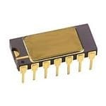
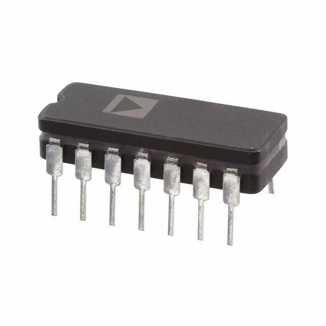
| 供应商器件封装 | 14-CDIP |
| 功能 | A complete, high accuracy, monolithic rms-to-dc converter that computes the true rms value of any complex waveform |
| 包装 | 管件 |
| 商标 | Analog Devices |
| 安装类型 | 通孔 |
| 安装风格 | Through Hole |
| 封装 | Tube |
| 封装/外壳 | 14-CDIP(0.300",7.62mm) |
| 封装/箱体 | SBDIP-14 |
| 工作温度范围 | 0 C to + 70 C |
| 工作电源电压 | 15 V |
| 工厂包装数量 | 25 |
| 标准包装 | 1 |
| 电压-电源 | ±3 V ~ 18 V |
| 电流-电源 | 2.2mA |
| 系列 | AD637 |
| 转换器数量 | 1 |
| 配用 | /product-detail/zh/AD637-EVALZ/AD637-EVALZ-ND/1534537 |


PDF Datasheet 数据手册内容提取
High Precision, Wideband RMS-to-DC Converter Data Sheet AD637 FEATURES FUNCTIONAL BLOCK DIAGRAM High accuracy BUFF IN + 0.02% maximum nonlinearity, 0 V to 2 V rms input BUFF OUT – 0.1% additional error to crest factor of 3 25kΩ Wide bandwidth RMS OUT 8 MHz at 2 V rms input VIN ABVSAOLLUUETE SDQIUVAIDREERR/ – 600 kHz at 100 mV rms + Computes DEN 25kΩ True rms INPUT – CAV Square + dB OUTPUT Mean square OUTPUT OFFSET Absolute value BIAS dCBhi opu stepleuctt (/6p0o dwBe rr-adnogwen) feature allows COMMON CS 00788-001 Analog three-state operation Figure 1. Quiescent current reduction from 2.2 mA to 350 µA GENERAL DESCRIPTION The AD637 is a complete, high accuracy, rms-to-dc converter facilitates the addition of precision rms measurement to remote that computes the true rms value of any complex waveform. It or handheld applications where minimum power consumption offers performance that is unprecedented in integrated circuit is critical. In addition, when the AD637 is powered down, the rms-to-dc converters and comparable to discrete and modular output goes to a high impedance state. This allows several techniques in accuracy, bandwidth, and dynamic range. The AD637s to be tied together to form a wideband true rms AD637 computes the true root mean square, mean square, or multiplexer. absolute value of any complex ac (or ac plus dc) input waveform The input circuitry of the AD637 is protected from overload and gives an equivalent dc output voltage. The true rms value of voltages in excess of the supply levels. The inputs are not a waveform is more useful than an average rectified signal damaged by input signals if the supply voltages are lost. because it relates directly to the power of the signal. The rms The AD637 is laser wafer trimmed to achieve rated performance value of a statistical signal relates to the standard deviation of without external trimming. The only external component the signal. required is a capacitor that sets the averaging period. The value Superior crest factor compensation permits measurements of this capacitor also determines low frequency accuracy, ripple of signals with crest factors of up to 10 with less than 1% level, and settling time. additional error. The wide bandwidth of the AD637 permits the The on-chip buffer amplifier is used either as an input buffer or measurement of signals up to 600 kHz with inputs of 200 mV rms in an active filter configuration. The filter can be used to reduce and up to 8 MHz when the input levels are above 1 V rms. the amount of ac ripple, thereby increasing accuracy. Direct dB value of the rms output with a range of 60 dB is The AD637 is available in accuracy Grade J and Grade K for available on a separate pin. An externally programmed commercial temperature range (0°C to 70°C) applications, accuracy reference current allows the user to select the 0 dB reference Grade A and Grade B for industrial range (−40°C to +85°C) appli- voltage to correspond to any level between 0.1 V and 2.0 V rms. cations, and accuracy Grade S rated over the −55°C to +125°C A chip select connection on the AD637 permits the user to temperature range. All versions are available in hermetically sealed, decrease the supply current from 2.2 mA to 350 µA during 14-lead SBDIP, 14-lead CERDIP, and 16-lead SOIC_W packages. periods when the rms function is not in use. This feature Rev. L Document Feedback Information furnished by Analog Devices is believed to be accurate and reliable. However, no responsibility is assumed by Analog Devices for its use, nor for any infringements of patents or other One Technology Way, P.O. Box 9106, Norwood, MA 02062-9106, U.S.A. rights of third parties that may result from its use. Specifications subject to change without notice. No license is granted by implication or otherwise under any patent or patent rights of Analog Devices. Tel: 781.329.4700 ©2015 Analog Devices, Inc. All rights reserved. Trademarks and registered trademarks are the property of their respective owners. Technical Support www.analog.com
AD637 Data Sheet TABLE OF CONTENTS Features .............................................................................................. 1 Offset Trim .............................................................................. 14 Functional Block Diagram .............................................................. 1 Scale Factor Trim ................................................................... 14 General Description ......................................................................... 1 Choosing the Averaging Time Constant ................................. 14 Revision History ............................................................................... 3 Frequency Response .................................................................. 16 Specifications ..................................................................................... 4 AC Measurement Accuracy and Crest Factor ........................ 17 Absolute Maximum Ratings .......................................................... 10 Connection for dB Output ........................................................ 17 ESD Caution ................................................................................ 10 dB Calibration ............................................................................. 18 Pin Configurations and Function Descriptions ......................... 11 Low Frequency Measurements ................................................. 19 Theory of Operation ...................................................................... 12 Vector Summation ..................................................................... 19 Applications Information .............................................................. 13 Evaluation Board ............................................................................ 21 Standard Connection ................................................................. 13 Outline Dimensions ....................................................................... 24 Chip Select ................................................................................... 13 Ordering Guide .......................................................................... 25 Optional Trims for High Accuracy .......................................... 13 Rev. L | Page 2 of 25
Data Sheet AD637 REVISION HISTORY 4/15—Rev. K to Rev. L 10/06—Rev. H to Rev. I Changes to Features Section, Figure 1, and General Description Changes to Table 1 ............................................................................ 3 Section ................................................................................................ 1 Changes to Figure 4 .......................................................................... 7 Changes to Table 1 ............................................................................ 4 Changes to Figure 7 .......................................................................... 9 Added Table 2; Renumbered Sequentially ..................................... 6 Changes to Figure 16, Figure 18, and Figure 19 .......................... 12 Added Table 3 .................................................................................... 8 Changes to Figure 20 ...................................................................... 13 Changed Pin NC to Pin NIC (Throughout) ................................ 11 12/05—Rev. G to Rev. H Changes to Theory of Operation Section and Figure 4 ............. 12 Changes to Figure 5......................................................................... 13 Updated Format ................................................................. Universal Changes to Optional Trims for High Accuracy Section and Changes to Figure 1 .......................................................................... 1 Figure 8; Added Offset Trim Section and Scale Factor Trim Changes to Figure 11 ...................................................................... 10 Section ............................................................................................... 14 Updated Outline Dimensions........................................................ 16 Changes to Choosing the Averaging Time Constant and Changes to Ordering Guide ........................................................... 17 Figure 11 ........................................................................................... 15 4/05—Rev. F to Rev. G Changes to Figure 20 ...................................................................... 19 Changes to Figure 21 ...................................................................... 20 Updated Format ................................................................. Universal Changes to Ordering Guide ........................................................... 26 Changes to Figure 1 .......................................................................... 1 Changes to General Description ..................................................... 1 2/11—Rev. J to Rev. K Deleted Product Highlights ............................................................. 1 Changes to Figure 15 ...................................................................... 11 Moved Figure 4 to Page .................................................................... 8 Changes to Figure 16 ...................................................................... 12 Changes to Figure 5 .......................................................................... 9 Changes to Evaluation Board Section and Figure 23 ................. 16 Changes to Figure 8 ........................................................................ 10 Added Figure 24; Renumbered Sequentially ............................... 17 Changes to Figure 11, Figure 12, Figure 13, and Figure 14 ....... 11 Changes to Figure 25 Through Figure 29 .................................... 17 Changes to Figure 19 ...................................................................... 14 Changes to Figure 30 ...................................................................... 18 Changes to Figure 20 ...................................................................... 14 Added Figure 31 .............................................................................. 18 Changes to Figure 21 ...................................................................... 16 Deleted Table 6; Renumbered Sequentially ................................. 18 Updated Outline Dimensions........................................................ 17 Changes to Ordering Guide ........................................................... 20 Changes to Ordering Guide ........................................................... 18 4/07—Rev. I to Rev. J 3/02—Rev. E to Rev. F Added Evaluation Board Section .................................................. 16 Edits to Ordering Guide ................................................................... 3 Updated Outline Dimensions ........................................................ 20 Rev. L | Page 3 of 25
AD637 Data Sheet SPECIFICATIONS At 25°C, test frequency = 1 kHz, V units are V , VS = ±15 V dc, unless otherwise noted. IN RMS Table 1. AD637J/AD637A Parameter Test Conditions/Comments Min Typ Max Unit TRANSFER FUNCTION VOUT = avg (VIN)2 CONVERSION ACCURACY Total Error, Internal Trim See Figure 5 ±1 ± 0.5 mV rms ±% of reading T to T ±3.0 ± 0.6 mV ± % of reading MIN MAX vs. Supply V = 300 mV 30 150 μV/V IN V = −300 mV 100 300 μV/V IN DC Reversal −2 V < V < +2 V 0.25 % of reading IN Nonlinearity 2 V full scale 0.04 % of FSR 7 V full scale 0.05 % of FSR Total Error External trim ±0.5 ± 0.1 mV ± % of reading ERROR VS. CREST FACTOR (CF) Additional, at 1 V rms CF, % For CF = 1 to 2 Specified accuracy For CF = 3 ±0.1 % of reading For CF = 10 ±1.0 % of reading AVERAGING TIME CONSTANT 25 ms/μF C AV INPUT CHARACTERISTICS Signal Range VS = ±15 V Continuous 0 to 7 V rms Transient ±15 V p-p VS = ±5 V Continuous 0 to 4 V rms Transient ±6 V p-p Input Resistance 6.4 8 9.6 kΩ Input Offset Voltage ±0.5 mV FREQUENCY RESPONSE Bandwidth for 1% (0.09 dB) Additional Error V = 20 mV 11 kHz IN V = 200 mV 66 kHz IN V = 2 V 200 kHz IN ±3 dB V = 20 mV 150 kHz IN V = 200 mV 1 MHz IN V = 2 V 8 MHz IN OUTPUT CHARACTERISTICS Offset Voltage ±1 mV vs. temperature ±0.05 ±0.089 mV/°C Voltage Swing, 2 kΩ load 0 to 12.0 13.5 V VS = ±3 V 0 to 2 2.2 V Output Current 6 mA Short-Circuit Current 20 mA Resistance CS high 0.5 Ω Resistance CS low 100 kΩ Rev. L | Page 4 of 25
Data Sheet AD637 AD637J/AD637A Parameter Test Conditions/Comments Min Typ Max Unit dB OUTPUT Error V = 7 mV to 7 V rms, 0 dBV ±0.5 dBV IN Scale Factor −3 mV/dB Scale Factor Tempco +0.33 % of reading/°C −0.033 dB/°C I for 0 dB = 1 V rms 5 20 80 µA REF I Range 1 100 µA REF BUFFER AMPLIFIER Input Output Voltage Range −V to (+V − 2.5) V S S Input Offset Voltage ±0.8 ±2 mV Input Current ±2 ±10 nA Input Resistance 108 Ω Output Current −0.13 +5 mA Short-Circuit Current 20 mA Small Signal Bandwidth 1 MHz Slew Rate 2 kΩ load, to −V 5 V/µs S DENOMINATOR INPUT Input Range 0 to 10 V Input Resistance 20 25 30 kΩ Offset Voltage ±0.2 ±0.5 mV CHIP SELECT (CS) RMS On Level Open or 2.4 < V < +V V C S RMS Off Level V < 0.2 V < 0.2 V C C I of Chip Select OUT CS low 10 µA CS high 0 µA On Time Constant 10 + ((25 kΩ) × C ) µs AV Off Time Constant 10 + ((25 kΩ) × C ) µs AV POWER SUPPLY Operating Voltage Range ±3.0 ±18 V Quiescent Current 2.2 3 mA Standby Current 350 450 µA Rev. L | Page 5 of 25
AD637 Data Sheet Table 2. AD637K/AD637B Parameter Test Conditions/Comments Min Typ Max Unit TRANSFER FUNCTION VOUT = avg (VIN)2 CONVERSION ACCURACY Total Error, Internal Trim See Figure 5 ±0.5 ± 0.2 mV rms ±% of reading T to T ±2.0 ± 0.3 mV ± % of reading MIN MAX vs. Supply V = 300 mV 30 150 μV/V IN V = −300 mV 100 300 μV/V IN DC Reversal −2 V < V < +2 V 0.1 % of reading IN Nonlinearity 2 V full scale 0.02 % of FSR 7 V full scale 0.05 % of FSR Total Error External trim ±0.25 ± 0.05 mV ± % of reading ERROR VS. CREST FACTOR (CF) Additional, at 1 V rms CF, % For CF = 1 to 2 Specified accuracy For CF = 3 ±0.1 % of reading For CF = 10 ±1.0 % of reading AVERAGING TIME CONSTANT 25 ms/μF C AV INPUT CHARACTERISTICS Signal Range VS = ±15 V Continuous 0 to 7 V rms Transient ±15 V p-p VS = ±5 V Continuous 0 to 4 V rms Transient ±6 V p-p Input Resistance 6.4 8 9.6 kΩ Input Offset Voltage ±0.2 mV FREQUENCY RESPONSE Bandwidth for 1% (0.09 dB) Additional Error V = 20 mV 11 kHz IN V = 200 mV 66 kHz IN V = 2 V 200 kHz IN ±3 dB V = 20 mV 150 kHz IN V = 200 mV 1 MHz IN V = 2 V 8 MHz IN OUTPUT CHARACTERISTICS Offset Voltage ±0.5 mV vs. temperature ±0.04 ±0.056 mV/°C Voltage Swing, 2 kΩ load 0 to 12.0 13.5 V VS = ±3 V 0 to 2 2.2 V Output Current 6 mA Short-Circuit Current 20 mA Resistance CS high 0.5 Ω Resistance CS low 100 kΩ dB OUTPUT Error V = 7 mV to 7 V rms, 0 dBV ±0.3 dBV IN Scale Factor −3 mV/dB Scale Factor Tempco +0.33 % of reading/°C −0.033 dB/°C I for 0 dB = 1 V rms 5 20 80 μA REF I Range 1 100 μA REF Rev. L | Page 6 of 25
Data Sheet AD637 AD637K/AD637B Parameter Test Conditions/Comments Min Typ Max Unit BUFFER AMPLIFIER Input Output Voltage Range −V to (+V − 2.5) V S S Input Offset Voltage ±0.5 ±1 mV Input Current ±2 ±5 nA Input Resistance 108 Ω Output Current −0.13 +5 mA Short-Circuit Current 20 mA Small Signal Bandwidth 1 MHz Slew Rate 2 kΩ load, to −V 5 V/μs S DENOMINATOR INPUT Input Range 0 to 10 V Input Resistance 20 25 30 kΩ Offset Voltage ±0.2 ±0.5 mV CHIP SELECT (CS) RMS On Level Open or 2.4 < V < +V V C S RMS Off Level V < 0.2 V C I of Chip Select OUT CS low 10 μA CS high 0 μA On Time Constant 10 + ((25 kΩ) × C ) μs AV Off Time Constant 10 + ((25 kΩ) × C ) μs AV POWER SUPPLY Operating Voltage Range ±3.0 ±18 V Quiescent Current 2.2 3 mA Standby Current 350 450 μA Rev. L | Page 7 of 25
AD637 Data Sheet Table 3. AD637S Parameter Test Conditions/Comments Min Typ Max Unit TRANSFER FUNCTION VOUT = avg (VIN)2 CONVERSION ACCURACY Total Error, Internal Trim See Figure 5 ±1 ± 0.5 mV rms ±% of reading T to T ±6 ± 0.7 mV ± % of reading MIN MAX vs. Supply V = 300 mV 30 150 μV/V IN V = −300 mV 100 300 μV/V IN DC Reversal −2 V < V < +2 V 0.25 % of reading IN Nonlinearity 2 V full scale 0.04 % of FSR 7 V full scale 0.05 % of FSR Total Error External trim ±0.5 ± 0.1 mV ± % of reading ERROR VS. CREST FACTOR (CF) Additional, at 1 V rms CF, % For CF = 1 to 2 Specified accuracy For CF = 3 ±0.1 % of reading For CF = 10 ±1.0 % of reading AVERAGING TIME CONSTANT 25 ms/μF C AV INPUT CHARACTERISTICS Signal Range VS = ±15 V Continuous 0 to 7 V rms Transient ±15 V p-p VS = ±5 V Continuous 0 to 4 V rms Transient ±6 V p-p Input Resistance 6.4 8 9.6 kΩ Input Offset Voltage ±0.5 mV FREQUENCY RESPONSE Bandwidth for 1% (0.09 dB) Additional Error V = 20 mV 11 kHz IN V = 200 mV 66 kHz IN V = 2 V 200 kHz IN ±3 dB V = 20 mV 150 kHz IN V = 200 mV 1 MHz IN V = 2 V 8 MHz IN OUTPUT CHARACTERISTICS Offset Voltage ±1 mV vs. temperature ±0.04 ±0.07 mV/°C Voltage Swing, 2 kΩ load 0 to 12.0 13.5 V VS = ±3 V 0 to 2 2.2 V Output Current 6 mA Short-Circuit Current 20 mA Resistance CS high 0.5 Ω Resistance CS low 100 kΩ dB OUTPUT Error V = 7 mV to 7 V rms, 0 dBV ±0.5 dBV IN Scale Factor −3 mV/dB Scale Factor Tempco +0.33 % of reading/°C −0.033 dB/°C I for 0 dB = 1 V rms 5 20 80 μA REF I Range 1 100 μA REF Rev. L | Page 8 of 25
Data Sheet AD637 AD637S Parameter Test Conditions/Comments Min Typ Max Unit BUFFER AMPLIFIER Input Output Voltage Range −V to (+V − 2.5) V S S Input Offset Voltage ±0.8 ±2 mV Input Current ±2 ±10 nA Input Resistance 108 Ω Output Current −0.13 +5 mA Short-Circuit Current 20 mA Small Signal Bandwidth 1 MHz Slew Rate 2 kΩ load, to −V 5 V/μs S DENOMINATOR INPUT Input Range 0 to 10 V Input Resistance 20 25 30 kΩ Offset Voltage ±0.2 ±0.5 mV CHIP SELECT (CS) RMS On Level Open or 2.4 < V < +V V C S RMS Off Level V I of Chip Select OUT CS low 10 μA CS high 0 μA On Time Constant 10 + ((25 kΩ) × C ) μs AV Off Time Constant 10 + ((25 kΩ) × C ) μs AV POWER SUPPLY Operating Voltage Range ±3.0 ±18 V Quiescent Current 2.2 3 mA Standby Current 350 450 μA Rev. L | Page 9 of 25
AD637 Data Sheet ABSOLUTE MAXIMUM RATINGS Stresses at or above those listed under Absolute Maximum Table 4. Ratings may cause permanent damage to the product. This is a Parameter Rating stress rating only; functional operation of the product at these ESD Rating 500 V or any other conditions above those indicated in the operational Supply Voltage ±18 V dc section of this specification is not implied. Operation beyond Internal Quiescent Power Dissipation 108 mW the maximum operating conditions for extended periods may Output Short-Circuit Duration Indefinite affect product reliability. Storage Temperature Range −65°C to +150°C Lead Temperature (Soldering 10 sec) 300°C ESD CAUTION Rated Operating Temperature Range AD637J, AD637K 0°C to 70°C AD637A, AD637B −40°C to +85°C AD637S, 5962-8963701CA −55°C to +125°C Rev. L | Page 10 of 25
Data Sheet AD637 PIN CONFIGURATIONS AND FUNCTION DESCRIPTIONS BUFF IN 1 14 BUFF OUT BUFF IN 1 16 BUFF OUT NIC 2 13 VIN NIC 2 15 VIN COMMON 3 AD637 12 NIC COMMON 3 AD637 14 NIC OUTPUT OFFSET 4 TOP VIEW 11 +VS OUTPUT OFFSET 4 TOP VIEW 13 +VS CS 5 (Not to Scale) 10 –VS CS 5 (Not to Scale) 12 –VS DEN INPUT 6 9 RMS OUT DEN INPUT 6 11 RMS OUT dB OUNTIPCU =T NO7 INTERNAL CONN8ECCTAIVON 00788-002 dB OUTNPINCUI CT= N78O INTERNAL CONN190ECCNTIACIOVN 00788-003 Figure 2. 14-Lead SBDIP/CERDIP Pin Configuration Figure 3. 16-Lead SOIC_W Pin Configuration Table 5. 14-Lead SBDIP/CERDIP Pin Function Descriptions Table 6. 16-Lead SOIC_W Pin Function Descriptions Pin No. Mnemonic Description Pin No. Mnemonic Description 1 BUFF IN Buffer Input 1 BUFF IN Buffer Input 2, 12 NIC No Internal Connection 2, 8, 9, 14 NIC No Internal Connection 3 COMMON Analog Common 3 COMMON Analog Common 4 OUTPUT OFFSET Output Offset 4 OUTPUT OFFSET Output Offset 5 CS Chip Select 5 CS Chip Select 6 DEN INPUT Denominator Input 6 DEN INPUT Denominator Input 7 dB OUTPUT dB Output 7 dB OUTPUT dB Output 8 CAV Averaging Capacitor Connection 10 CAV Averaging Capacitor Connection 9 RMS OUT RMS Output 11 RMS OUT RMS Output 10 −VS Negative Supply Rail 12 −VS Negative Supply Rail 11 +VS Positive Supply Rail 13 +VS Positive Supply Rail 13 VIN Signal Input 15 VIN Signal Input 14 BUFF OUT Buffer Output 16 BUFF OUT Buffer Output Rev. L | Page 11 of 25
AD637 Data Sheet THEORY OF OPERATION FILTER/AMPLIFIER BUFF OUT 14 SOQNUEA RQEURA/DDIRVAIDNETR 24kΩ 8 CAV BUFFER BUFF IN 1 AMPLIFIER 11 +VS A5 I4 A4 9 ROMUTS dB 24kΩ I1 7 OUTPUT 3 COMMON Q4 Q1 ABSOCULURTREENVTA LCUOEN VVOERLTTAEGRETO Q5 BIAS 5 CS DEN 6 INPUT 6kΩ 6kΩ Q2 Q3 A3 I3 24kΩ OUTPUT 4 OFFSET A2 12kΩ 125Ω VIN 13 AD637 A1 10 –VS 00788-004 Figure 4. Simplified Schematic The AD637 embodies an implicit solution of the rms equation and that overcomes the inherent limitations of straightforward rms V = V rms OUT IN computation. The actual computation performed by the AD637 follows the equation: To compute the absolute value of the input signal, the averaging capacitor is omitted. However, a small capacitance value at the V 2 V rms Avg IN averaging capacitor pin is recommended to maintain stability; V rms 5 pF is sufficient for this purpose. The circuit operates identically to that of the rms configuration, except that I is now equal to 3 Figure 4 is a simplified schematic of the AD637, subdivided I, giving 4 into four major sections: absolute value circuit (active rectifier), squarer/divider, filter circuit, and buffer amplifier. The input I 2 I 1 voltage (V ), which can be ac or dc, is converted to a unipolar 4 I IN 4 current (I) by the A1 and A2 absolute value circuit. I drives 1 1 I = |I| 4 1 one input of the squarer/divider, which has the transfer function: The denominator current can also be supplied externally by I 2 I 1 providing a reference voltage (V ) to Pin 6. The circuit operates 4 I REF 3 identically to the rms case, except that I is now proportional to 3 V . Therefore, The output current of the squarer/divider, I, drives A4, forming REF 4 a low-pass filter with the external averaging capacitor. If the RC I 2 I Avg 1 time constant of the filter is much greater than the longest period 4 I 3 of the input signal, then the A4 output is proportional to the average of I4. The output of this filter amplifier is used by A3 and to provide the denominator current I, which equals Avg I and 3 4 V 2 is returned to the squarer/divider to complete the implicit rms V IN OUT V computation DEN I 2 This is the mean square of the input signal. I4 Avg I14 I1rms Rev. L | Page 12 of 25
Data Sheet AD637 APPLICATIONS INFORMATION STANDARD CONNECTION 20 The AD637 is simple to connect for a majority of rms measurements. In the standard rms connection shown in Figure 5, d) 15 a only a single external capacitor is required to set the averaging Lo Ω time constant. In this configuration, the AD637 computes the k 2 s true rms of any input signal. An averaging error, the magnitude olt 10 V of which is dependent on the value of the averaging capacitor, (UT is present at low frequencies. For example, if the filter capacitor, VO X C , is 4 µF, the error is 0.1% at 10 Hz and increases to 1% at A AV M 5 3 Hz. To measure ac signals, the AD637 can be ac-coupled by adding a nonpolar capacitor in series with the input, as shown in Figure 5. 00 ±3SUPP±5LY VOLTAGE – ±D1U0AL SUPPLY (V±)15 ±18 00788-006 1 BUFF IN + AD637 BUFF OUT 14 Figure 6. Maximum VOUT vs. Supply Voltage – NC 2 NIC ABVSAOLLUUETE VIN 13 VIN CHIP SELECT 3 COMMON The AD637 includes a chip select feature that allows the user +VS SQUARER/ NIC 12(OPTIONAL) to decrease the quiescent current of the device from 2.2 mA to 4.7kΩ 4 OOUFFTSPEUTT BIAS DIVIDER +VS 11 +VS 350 µA. This is done by driving CS, Pin 5, to below 0.2 V dc. Under these conditions, the output goes into a high impedance 5 CS 10 –VS –VS state. In addition to reducing the power consumption, the 6 DINEPNUT25kΩ – ROMUST 9 VOUT = VIN2 outputs of multiple devices can be connected in parallel to – + + CAV form a wide bandwidth rms multiplexer. Tie Pin 5 high to 7 dOBUTPUT + 25kΩ CAV 8 disable the chip select. OPTIONAL TRIMS FOR HIGH ACCURACY NIC = NO INTERNAL CONNECTION 00788-005 The AD637 includes provisions for trimming out output offset Figure 5. Standard RMS Connection and scale factor errors resulting in significant reduction in the maximum total error, as shown in Figure 7. The residual error is The performance of the AD637 is tolerant of minor variations due to a fixed input offset in the absolute value circuit and the in the power supply voltages; however, if the supplies used residual nonlinearity of the device. exhibit a considerable amount of high frequency ripple, it is advisable to bypass both supplies to ground through a 0.1 µF 5.0 ceramic disc capacitor placed as close to the device as possible. AD637K MAX The output signal range of the AD637 is a function of the 2.5 INTERNAL TRIM supply voltages, as shown in Figure 6. Use the output voltage buffered or nonbuffered, depending on the characteristics of the mV) load. Connect the buffer input (Pin 1) to common if buffering is OR ( 0 EXTEARDN6A37LK TRIM R not required. The output of the AD637 is capable of driving R E 5 mA into a 2 kΩ load without degrading the accuracy of the device. –2.5 AD637K: 0.5mV ± 0.2% 0.25mV ± 0.05% EXTERNAL –5.00 0.5 INPUT L1E.0VEL (V) 1.5 2.0 00788-007 Figure 7. Maximum Total Error vs. Input Level AD637K Internal and External Trims Rev. L | Page 13 of 25
AD637 Data Sheet Referring to Figure 8 for optional external gain and offset trim The value of C and the 25 kΩ feedback resistor establish the AV schematic. The following sections describe trimming for greater averaging time constant, and solely determines the magnitude accuracy in detail. of the rms-to-dc conversion error. Furthermore, any post- conversion filtering does not improve the dc component Offset Trim composite result. Ground the input signal (V ) and adjust R1 until the output IN voltage at Pin 9 measures 0 V. Alternatively, apply the least Equation 1 defines the approximate peak value of the ac ripple expected value of V .at the input V and adjust R1 until the dc component of the composite output. IN IN output voltage at Pin 9 measures the same value as the rms input. 50 in%of readingwhere(τ>1/ f) (1) Scale Factor Trim 6.3τf Insert Resistor R4 in series with the input to decrease the range EO of the scale factor. Connect a precision source to Pin 13 and IDEAL adjust the output for the desired full-scale input to V , using EO IN DC ERROR = AVERAGE OF OUTPUT – IDEAL either a calibrated dc or 1 kHz ac voltage, and adjust Resistor R3 to give the correct output at Pin 9 (that is, 1 V rms at the input AVERAGE ERROR results in a dc output voltage of 1.000 V dc). A 2 V p-p sine wave input yields 0.707 V dc at the output. Remaining errors DOUBLE-FREQUENCY are due to the nonlinearity. RIPPLE TIME 00788-009 Figure 9. Enlarged Composite Conversion Result for a Sinusoidal Input 1 BUFF IN AD637 BUFF + OUT 14 – NC R4 Increasing the value of the averaging capacitor or adding a post- 2 NIC ABVSAOLLUUETE VIN 13 147Ω VIN rms filter network reduces the ripple error. OUTPUT OFFSET 3 COMMON TRIM NIC 12 The dc error appears as a frequency dependent offset at the 50+kRVΩ1S 1RM2Ω 4 OOUFFTSPEUTT BIAS SDQIUVAIDREERR/ +VS 11 +VS output of the AD637 and follows the relationship –VS +VS 4.7kΩ5 CS –VS 10 –VS 1 in%of reading DEN RMS 0.16+6.4τ2f2 6 INPUT 25kΩ – OUT 9 – RMSOUT dB + +25kΩ + CAV 100 7 OUTPUT CAV 8 g) n SCALEFACTOR TRIM di a e R NIC = NO INTERNAL CONNECTION 1Rk3Ω 00788-008 E (% of 10 Figure 8. Optional External Gain and Offset Trims PL P PEAK RIPPLE RI CHOOSING THE AVERAGING TIME CONSTANT OR R 1.0 O The AD637 computes the true rms value of both dc and ac R R DC ERROR E input signals. For dc inputs, the output tracks the absolute C D value of the input exactly. However, when the voltage is ac, tthhee ocroentivcearlt remd sd cv aoluutep ouft tvhoel tiangpeu ats. yTmhep tdoetivciaaltliyo nap fproroma cthhees i dtheea l 0.110 SINE W10A0VE INPUT FREQUE1NkCY (Hz) 10k 00788-010 rms value is due to the implicit denominator inherent to averag- Figure 10. Comparison of Percent DC Error to the Percent Peak Ripple over ing over an infinite time span. Because the error diminishes as Frequency Using the AD637 in the Standard RMS Connection with a 1 × µF CAV the averaging period increases, it quickly becomes negligible. The ac ripple component of averaging error is greatly reduced The remaining error components are the ac ripple and dc offset by increasing the value of the averaging capacitor. However, the voltage, if any. The ac and averaging error components are both value of the averaging capacitor increases exponentially while functions of the input-frequency (f) and the averaging time the settling time increases directly proportion to the value of constant τ (τ: 25 ms/µF of averaging capacitance). Figure 9 shows the averaging capacitor (T = 115 ms/µF of averaging capacitance). the output errors, which are enlarged for clarity. The frequency S of the ac component (ripple) is twice the frequency of the input, the dc error is the RSS sum of the average rectified error and any fixed value dc offset. Rev. L | Page 14 of 25
Data Sheet AD637 A preferable ripple reduction method is to use a post conversion 100 100 raroii nppsieppn llogeerl aeatt-nwtpdeoon -sluepe12 atofttiNBllileiIUotCn eFnlgroF. w IgtNii-mvpeeas+–.s tsUh fseiel tb etAehrsD,e ta6 tos3w v7soehAr-oapBVwlSoAlO nLlceLU oiU ESnmTa EFplBliOreUgVonUFuImTFN-rKei11s e431ey1 bfV. oeIUNrtw smueaeolnrlye REQUIRED C (µF)AV101..001 10% ERRO1%R ERRO0R.1% ERR0.O0R1% ERROR 1100..01 R 1% SETTLING TIME IN SECONDSMULTIPLY READING BY 0.115 3 COMMON + O NIC 12 C3 F OUTPUT SQUARER/ 4.7kΩ45 OCSFFSET BIAS DDIIVVIIDDEERR +VS 1110 +VS 0.011 10 INPU1T0 0FREQUENC1Yk (Hz) 10k 1000k.01 00788-012 +VS –VS –VS Figure 12. Values for CAV and 1% Settling Time for Stated % of Reading; Averaging DEN RMS Error (% DC Error + % Ripple (Peak)); Accuracy Includes ±20% Component 6 INPUT 25kΩ – – OUT 9 Tolerance dB + +25kΩ + CAV 7 OUTPUT CAV 8 100 100 S D N O0 2R4kXΩ 24kΩ C2) 10 10 SEC0.40 +FNiICg uC=2 rNeO 1 I2NT sEhRoNwALs CvOaNlFuNigeEusC rToeIf O1 CN1.A 2V- aPnolde Sthalele cno-Krreeys Fpilotenrd iFnAILgFNTO DaER vRR Ae ES rM1Ha OOPgVORinETL EgCR 3X 00788-011 REQUIRED C (AND AVC2 = 3.3 × CAV0.11 5% E1R%R E0OR.R1R%O0 .ER0R1%RO ERRROR 10.1 R 1% SETTLING TIME IN MULTIPLY READING BY error as a function of sine wave frequency for the standard rms O F connection. The 1% settling time is shown on the right side of Figure 12. 0.011 10 INPU1T0 0FREQUENC1kY (Hz) 10k 1000k.01 00788-013 Figure 13 shows the relationship between the averaging error, Figure 13. Values of CAV, C2, and 1% Settling Time for Stated % of Reading for signal frequency settling time, and averaging capacitor value. 1-Pole Post Filter; Averaging Error (% DC Error + % Ripple (Peak) Accuracy Figure 13 is drawn for filter capacitor values of 3.3× the ±20% Due to Component Tolerance) averaging capacitor value. This ratio sets the magnitude of 100 100 the ac and dc errors equal at 50 Hz. As an example, by using a S 1 µF averaging capacitor and a 3.3 µF filter capacitor, the ripple D N fufsFfuooieisslrlrttiitte nneatlrihggr .n6 eTCtFg0 hdi h atgeHeipiu smsaaz rivg creeieiein vt1rodopea3n rsuvg. l taiCyan l sAuifginaVge cccn aotarnaoepfld raa a i sovcsFei efirst lro3e tabed0rgyr uair nCacleo egdafnda upeec carf trrttcoioooiortm r o0no ar. f1i5 n Cn35.d3 .%2r %Ts ic peuh atpostenflli e in vtbn,hga ega le tn uc thrideaemesl a cy 1oedue- ftilbp n atyotgh el eed REQUIRED C (AND C2 + C3)AVC2 = C3 = 2.2 × CAV01.011 5% E1R%R E0O.R1RR%O0 E.R0R1R%O ERRROR 1100.1 R 1% SETTLING TIME IN SECOMULTIPLY READING BY 0.365 O The symmetry of the input signal also has an effect on the F mcoamgpnoitnuednet ovfa tlhuee sa vfoerr avgairniogu esr rtoyrp. eTsa obfl e6 07 Hgizv eisn pthuet spirgancatilcs.a l 0.011 10 INP1U0T0 FREQUEN1CkY (Hz) 10k 1000k.01 00788-014 These capacitor values can be directly scaled for frequencies Figure 14. Values of CAV, C2, and C3 and 1% Settling Time for Stated % of other than 60 Hz—that is, for 30 Hz, these values are doubled, Reading for 2-Pole Sallen-Key Filter; Averaging Error (% DC Error + %Ripple and for 120 Hz they are halved. (Peak) Accuracy ±20% Due to Component Tolerance) Use Figure 14 to determine the required value of C , C2, and AV C3 for the desired level of ripple and settling time. Rev. L | Page 15 of 25
AD637 Data Sheet Table 7. Practical Values of C and C2 for Various Input Waveforms AV Absolute Value Recommended Standard Values for CAV and C2 Input Waveform Circuit Waveform Minimum R × C for 1% Averaging Error @ 60 Hz with T = 16.6 ms 1% Settling AV and Period and Period Time Constant C (μF) C2 (μF) Time AV T 1/2T 1/2T 0.47 1.5 181 ms A 0V Symmetrical Sine Wave T T T 0.82 2.7 325 ms B 0V Sine Wave with dc Offset T T 10 (T − T2) 6.8 22 2.67 sec C T2 0V T2 Pulse Train Waveform T T 10 (T − 2T2) 5.6 18 2.17 sec D T2 0V T2 FREQUENCY RESPONSE The frequency response of the AD637 at various signal levels is shown in Figure 15. The dashed lines show the upper frequency 10 7V RMS INPUT limits for 1%, 10%, and ±3 dB of additional error. For example, 2V RMS INPUT note that for 1% additional error with a 2 V rms input, the 1V RMS INPUT 1 hbeig mheesats ufrreeqdu wenitchy 1 a%ll oerwroabr laet issi g2n0a0l fkrHeqzu. eAn c2i0es0 ump Vto s 1ig0n0 aklH cazn. (V)OUT 1% 10% ±3dB V 100mV RMS INPUT 0.1 To take full advantage of the wide bandwidth of the AD637, use care in the selection of the input buffer amplifier. To ensure 0.01 that the input signal is accurately presented to the converter, 10mV RMS INPUT the input buffer must have a −3 dB bandwidth that is wider tthhiasn a pthpalitc oatfi othne. FAoDr e6x3a7m. Nploet, et hteh em iimnipmourtman scleew o fr astlee wre qrautiere idn 1k 10k INPUT FRE1Q00UkENCY (Hz) 1M 10M 00788-015 for a 1 V rms, 5 MHz, sine wave input signal is 44 V/μs. The user Figure 15. Frequency Response is cautioned that this is the minimum rising or falling slew rate and that care must be exercised in the selection of the buffer amplifier, because some amplifiers exhibit a two-to-one difference between rising and falling slew rates. The AD845 is recommended as a precision input buffer. Rev. L | Page 16 of 25
Data Sheet AD637 1.5 AC MEASUREMENT ACCURACY AND CREST FACTOR 1.0 Crest factor is often overlooked in determining the accuracy of %) an ac measurement. Crest factor is defined as the ratio of the peak R ( 0.5 O signal amplitude to the rms value of the signal (CF = VP/V rms). RR Most common waveforms, such as sine and triangle waves, have N E 0 relatively low crest factors (≤2). Waveforms that resemble low SE I A duty cycle pulse trains, such as those occurring in switching RE–0.5 C power supplies and SCR circuits, have high crest factors. For N POSITIVE INPUT PULSE I CAV = 22µF example, a rectangular pulse train with a 1% duty cycle has –1.0 a crest factor of 10 (CF = 1 ). 0Vp100µs Te0 η eC=IF ND (=UR TM1/YS )C η=Y C1 LVE R =M1S00Tµs 00788-016 –1.51 2Figur3e 18. A4dditCio5RnESaTl EF6rAroCrT vO7sR. Cres8t Fact9or 10 11 00788-018 Figure 16. Duty Cycle Timing 2.0 10 evel) 1.8 L S 1.6 CAV = 22µF RM of 1.4 % E IN ERROR (%) 1 CF = 10 DE OF ERROR ( 1001....2680 CCFF == 170 S U A T INCRE 0.1 MAGNI 00..42 CF = 3 0.011 10PULSE WIDTH (µs)100 CF = 3 1000 00788-017 Figur0e0 19. Error vs. R0M.5S Input LVeINv e(1Vl .f 0RoMr TSh)ree Com1.m5on Crest Fa2c.t0or00788-019s Figure 17. AD637 Error vs. Pulse Width Rectangular Pulse CONNECTION FOR dB OUTPUT Another feature of the AD637 is the logarithmic, or decibel, Figure 18 is a curve of additional reading error for the AD637 output. The internal circuit that computes dB works well over for a 1 V rms input signal with crest factors from 1 to 11. a 60 dB range. Figure 20 shows the dB measurement connection. A rectangular pulse train (pulse width 100 μs) is used for this The user selects the 0 dB level by setting R1 for the proper 0 dB test because it is the worst-case waveform for rms measurement reference current, which is set to cancel the log output current (all the energy is contained in the peaks). The duty cycle and from the squarer/divider circuit at the desired 0 dB point. The peak amplitude were varied to produce crest factors from l to external op amp is used to provide a more convenient scale and to 10 while maintaining a constant 1 V rms input amplitude. allow compensation of the 0.33%/°C temperature drift of the dB circuit. The temperature resistor, R3, as shown in Figure 20, is available from Precision Resistor Co., Inc., in Largo, Fla. (Model PT146). Rev. L | Page 17 of 25
AD637 Data Sheet dB CALIBRATION Refer to Figure 20: • Set V = 1.00 V dc or 1.00 V rms IN • Adjust R1 for 0 dB output = 0.00 V • Set V = 0.1 V dc or 0.10 V rms IN • Adjust R2 for dB output = −2.00 V Any other dB reference can be used by setting V and R1 IN accordingly. R2 dB SCALE FACTOR SIGNAL 33.2kΩ ADJUST INPUT 5kΩ BUFFER AD637 BUFF R3 +VS 1 BUFFIN OUT 14 1kΩ* 60.4Ω 2 7 6 2 NIC VIN 13 AD707JN ABVSAOLLUUETE 3 4 CdBO MOPUETNPSUATTED +100mV/dB 3 COMMON NIC 12 BIAS –VS OUTPUT SECTION 4 OFFSET SQUARER/DIVIDER 11 +VS +VS +VS 4.7kΩ 5 CS –VS 10 –VS 6 DINEPNUT 25kΩ ROMUTS 9 25kΩ + 1µF 7 dB OUTPUT FILTER CAV 8 10kΩ +VS R1 500kΩ +2.5V AD508J 0dB ADJUST *1kΩ + 3500ppm N SICE E= TNEOX ITNTERNAL CONNECTION 00788-020 Figure 20. dB Connection Rev. L | Page 18 of 25
Data Sheet AD637 1µF V+ 3.3MΩ 3.3MΩ 3 7 6 1 BUFF IN BUFFER AD637 BOUUFFT 14 1µF 2 AD548JN FILTERED 4 V RMS OUTPUT 2 NIC ABSOLUTE VIN 13 SIGNAL V– VALUE INPUT 6.8MΩ +VS 3 COMMON NIC 12 BIAS OUTPUT 1MΩ OOUFFTSPEUTT SECTION SQUARER/ 11 1000pF OFFSET 50kΩ 4 DIVIDER +VS +VS ADJUST +VS 5 CS –VS 10 –VS –VS 4.7kΩ DEN RMS 6 INPUT25kΩ OUT 9 VIN2 + V RMS 100µF 25kΩ dB OUTPUT CAV 8 7 499kΩ1% CAV1 R 3.3µF N12..O NVTAICELS =U ENSO C INHTOESRENNA TLO C GOINVNEE 0C.1T%IO ANV.ERAGING ERROR AT 1Hz. 00788-021 Figure 21. AD637 as a Low Frequency RMS Converter LOW FREQUENCY MEASUREMENTS VECTOR SUMMATION If the frequencies of the signals to be measured are below 10 Hz, Use two AD637s for vector summation as shown in Figure 22. the value of the averaging capacitor required to deliver even 1% Here, the averaging capacitors are omitted (nominal 100 pF averaging error in the standard rms connection becomes capacitors are used to ensure stability of the filter amplifier), and extremely large. Figure 21 shows an alternative method of the outputs are summed as shown. The output of the circuit is obtaining low frequency rms measurements. Determine the V = V 2 +V 2 averaging time constant by the product of R and CAV1, in this OUT X Y circuit, 0.5 sec/µF of C . This circuit permits a 20:1 reduction AV This concept can be expanded to include additional terms by in the value of the averaging capacitor, permitting the use of feeding the signal from Pin 9 of each additional AD637 through high quality tantalum capacitors. It is suggested that the 2-pole, a 10 kΩ resistor to the summing junction of the AD711 and Sallen-Key filter shown in Figure 21 be used to obtain a low tying all of the denominator inputs (Pin 6) together. ripple level and minimize the value of the averaging capacitor. If C is added to IC1 in this configuration, then the output is If the frequency of interest is below 1 Hz, or if the value of AV the averaging capacitor is still too large, increase the 20:1 ratio. V 2 +V 2 X Y This is accomplished by increasing the value of R. If this is done, it is suggested that a low input current, low offset voltage If the averaging capacitor is included on both IC1 and IC2, the amplifier, such as the AD548, be used instead of the internal output is buffer amplifier. This is necessary to minimize the offset error introduced by the combination of amplifier input currents and V 2+V 2 X Y the larger resistance. This circuit has a dynamic range of 10 V to 10 mV and is limited only by the 0.5 mV offset voltage of the AD637. The useful bandwidth is 100 kHz. Rev. L | Page 19 of 25
AD637 Data Sheet EXPANDABLE BUFFER AD637 BUFF BUFF IN IC1 OUT 1 14 2 NIC ABSOLUTE VXIN 13 VALUE 3 COMMON NIC 12 BIAS 4 OOUFFTSPEUTT SECTION SQUARER/DIVIDER 11 +VS +VS +VS 5 CS 25kΩ –VS 10 –VS 4.7kΩ DEN RMS 6 INPUT 25kΩ OUT 9 dB OUTPUT FILTER 100pF 5pF CAV 7 8 10kΩ 10kΩ BUFFER IC2 AD637 BUFF 1 BUFF IN OUT 14 2 NIC ABSOLUTE VYIN 13 AD711K VALUE 3 COMMON NIC 12 10kΩ BIAS OUTPUT SECTION 4 OFFSET SQUARER/DIVIDER +VS 11 +VS 20kΩ +VS 5 CS 25kΩ –VS 10 –VS 4.7kΩ DEN RMS 6 INPUT 25kΩ OUT 9 100pF FILTER 8 dB OUTPUT 7 NIC = NO INTERNAL CONNECTION VOUT = VX2 + VY2 00788-022 Figure 22. Vector Sum Configuration Rev. L | Page 20 of 25
Data Sheet AD637 EVALUATION BOARD amp, and is configured on the AD637-EVALZ as a low-pass Figure 23 shows a digital image of the AD637-EVALZ, an Sallen-Key filter whose f < 0.5 Hz. Users can connect to evaluation board specially designed for the AD637. It is C the buffer by moving the FILTER switch to the on position. available at www.analog.com and is fully tested and ready DC_OUT is still the output of the AD637, and the test loop, for bench testing after connecting power and signal I/O. The BUF_OUT, is the output of the buffer. The R2 trimmer adjusts circuit is configured for dual power supplies, and standard the output offset voltage. BNC connectors serve as the signal input and output ports. The LPF frequency is changed by changing the component Referring to the schematic in Figure 30, the input connector values of CF1, CF2, R4, and R5. See Figure 24 and Figure 30 RMS_IN is capacitively coupled to Pin 15 (V of SOIC package) IN to locate these components. Note that a wide range of capacitor of the AD637. The DC_OUT connector is connected to Pin 11, and resistor values can be used with the AD637 buffer amplifier. RMS OUT, with provisions for connections to the output buffer between Pin 1 and Pin 16. The buffer is an uncommitted op 00788-123 Figure 23. AD637-EVALZ Rev. L | Page 21 of 25
AD637 Data Sheet 00788-124 00788-127 Figure 24. AD637-EVALZ Assembly Figure 27. Evaluation Board—Secondary Side Copper 00788-125 00788-128 Figure 25. Component Side Silkscreen Figure 28. Evaluation Board—Internal Power Plane 00788-126 00788-129 Figure 26. Evaluation Board—Component Side Copper Figure 29. Evaluation Board—Internal Ground Plane Rev. L | Page 22 of 25
AD637 Data Sheet GND1 GND2 GND3 GND4 –VS +VS C1 +C2 10µF 10µF 25V + 25V –VS +VS BUF_IN FILTER 4 1 OUT 2 5 3 IN 6 1 16 BUFF IN BUFF OUT BUF_OUT RMS_IN 2 NIC ADZ6137 VIN 15 + RMS_IN CIN +VS 3 COMMON NIC 14 2126µVF R1 50kRΩ2 1MΩ R3 4 OOUFFTSPEUTT +VS 13 C0.31µF +VS –VS +VS 4.7kΩ 5 CS –VS 12 C0.41µF –VS DC_OUT 6 11 DEN INPUT RMS OUT DC_OUT +CAV 22µF 7 10 dB OUTPUT CAV 16V DB_OUT 8 NIC NIC 9 + CF1 R5 47µF 24R.34kΩ 24.3kΩ 25V +CF2 47µF NIC 2=5 NVO INTERNAL CONNECTION 00788-130 Figure 30. Evaluation Board Schematic AC OR DC INPUT SIGNAL SOURCE FROM PRECISION CALIBRATOR OR FUNCTION GENERATOR POWER SUPPLY PRMEOCNISITIOONR DVMOMU TTO 00788-131 Figure 31. AD637-EVALZ Typical Bench Configuration Rev. L | Page 23 of 25
AD637 Data Sheet OUTLINE DIMENSIONS 0.005 (0.13) MIN 0.080 (2.03) MAX 14 8 0.310 (7.87) 1 0.220 (5.59) 7 PIN 1 0.100 (2.54) BSC 0.320 (8.13) 0.765 (19.43) MAX 0.290 (7.37) 0.200 (5.08) 0.060 (1.52) MAX 0.015 (0.38) 0.150 (3.81) 0.200 (5.08) MIN 0.125 (3.18) 0.070 (1.78) SPELAANTIENG 00..001058 ((00..3280)) 0.023 (0.58) 0.030 (0.76) 0.014 (0.36) CONTROLLING DIMENSIONS ARE IN INCHES; MILLIMETER DIMENSIONS (IN PARENTHESES) ARE ROUNDED-OFF INCH EQUIVALENTS FOR REFERENCE ONLY AND ARE NOT APPROPRIATE FOR USE IN DESIGN Figure 32. 14-Lead Side-Brazed Ceramic Dual In-Line Package [SBDIP] (D-14) Dimensions shown in inches and (millimeters) 0.005 (0.13) MIN 0.098 (2.49) MAX 14 8 0.310 (7.87) 0.220 (5.59) 1 7 PIN 1 0.100 (2.54) BSC 0.320 (8.13) 0.290 (7.37) 0.785 (19.94) MAX 0.060 (1.52) 0.200 (5.08) 0.015 (0.38) MAX 0.150 0.200 (5.08) (3.81) 0.125 (3.18) MIN SEATING 0.015 (0.38) 0.023 (0.58) 0.070 (1.78) PLANE 15° 0.008 (0.20) 0.014 (0.36) 0.030 (0.76) 0° CONTROLLING DIMENSIONS ARE IN INCHES; MILLIMETER DIMENSIONS (IN PARENTHESES) ARE ROUNDED-OFF INCH EQUIVALENTS FOR REFERENCE ONLY AND ARE NOT APPROPRIATE FOR USE IN DESIGN. Figure 33. 14-Lead Ceramic Dual In-Line Package [CERDIP] (Q-14) Dimensions shown in inches and (millimeters) Rev. L | Page 24 of 25
Data Sheet AD637 10.50(0.4134) 10.10(0.3976) 16 9 7.60(0.2992) 7.40(0.2913) 1 8 10.65(0.4193) 10.00(0.3937) 1.27(0.0500) 0.75(0.0295) BSC 2.65(0.1043) 0.25(0.0098) 45° 0.30(0.0118) 2.35(0.0925) 8° 0.10(0.0039) 0° COPLANARITY 0.10 0.51(0.0201) SPLEAATNIENG 0.33(0.0130) 1.27(0.0500) 0.31(0.0122) 0.20(0.0079) 0.40(0.0157) C(RINOEFNPEATRRREOENNLCLTEIHNCEOGOSNDMELISPYM)LAEAIANNRNDSETIAORTRNOOESUJNANEORDDETEEDAICN-POSMPFTRIFALONLMPIDMIRLAELIRATIMTDEEESRTFSMEO;SRIRN-0ECU1QH3SU-EADIVAIINMAELDENENSSTIIOGSNNFS.OR 03-27-2007-B Figure 34. 16-Lead Standard Small Outline Package [SOIC_W] Wide Body (RW-16) Dimensions shown in millimeters and (inches) ORDERING GUIDE Model1 Notes Temperature Range Package Description Package Option 5962-8963701CA 2 −55°C to +125°C 14-Lead CERDIP Q-14 AD637AQ −40°C to +85°C 14-Lead CERDIP Q-14 AD637ARZ −40°C to +85°C 16-Lead SOIC_W RW-16 AD637BRZ −40°C to +85°C 16-Lead SOIC_W RW-16 AD637JD 0°C to 70°C 14-Lead SBDIP D-14 AD637JDZ 0°C to 70°C 14-Lead SBDIP D-14 AD637JQ 0°C to 70°C 14-Lead CERDIP Q-14 AD637JRZ 0°C to 70°C 16-Lead SOIC_W RW-16 AD637JRZ-RL 0°C to 70°C 16-Lead SOIC_W RW-16 AD637JRZ-R7 0°C to 70°C 16-Lead SOIC_W RW-16 AD637KDZ 0°C to 70°C 14-Lead SBDIP D-14 AD637KQ 0°C to 70°C 14-Lead CERDIP Q-14 AD637KRZ 0°C to 70°C 16-Lead SOIC_W RW-16 AD637SD −55°C to +125°C 14-Lead SBDIP D-14 AD637SD/883B −55°C to +125°C 14-Lead SBDIP D-14 AD637SQ/883B −55°C to +125°C 14-Lead CERDIP Q-14 AD637-EVALZ Evaluation Board 1 Z = RoHS Compliant Part. 2 A standard microcircuit drawing is available. ©2015 Analog Devices, Inc. All rights reserved. Trademarks and registered trademarks are the property of their respective owners. D00788-0-4/15(L) Rev. L | Page 25 of 25
Mouser Electronics Authorized Distributor Click to View Pricing, Inventory, Delivery & Lifecycle Information: A nalog Devices Inc.: AD637KDZ 5962-8963701CA AD637JRZ AD637SQ/883B AD637BRZ AD637ARZ AD637-EVALZ AD637SD AD637AR AD637JRZ-RL AD637KRZ AD637JD AD637JQ AD637AQ AD637SD/883B AD637KQ AD637JDZ AD637JRZ-R7