ICGOO在线商城 > 集成电路(IC) > PMIC - RMS 至 DC 转换器 > AD536AKHZ
 Datasheet下载
- 型号: AD536AKHZ
- 制造商: Analog
- 库位|库存: xxxx|xxxx
- 要求:
| 数量阶梯 | 香港交货 | 国内含税 |
| +xxxx | $xxxx | ¥xxxx |
查看当月历史价格
查看今年历史价格
AD536AKHZ产品简介:
ICGOO电子元器件商城为您提供AD536AKHZ由Analog设计生产,在icgoo商城现货销售,并且可以通过原厂、代理商等渠道进行代购。 AD536AKHZ价格参考。AnalogAD536AKHZ封装/规格:PMIC - RMS 至 DC 转换器, RMS to DC Converter TO-100-10。您可以下载AD536AKHZ参考资料、Datasheet数据手册功能说明书,资料中有AD536AKHZ 详细功能的应用电路图电压和使用方法及教程。
AD536AKHZ 是由 Analog Devices Inc.(ADI)生产的一款 PMIC(电源管理集成电路),属于 RMS 至 DC 转换器类别。该器件的主要功能是将交流信号的均方根值(RMS)转换为直流电压输出,广泛应用于需要精确测量交流信号幅值的场景。以下是 AD536AKHZ 的主要应用场景:

1. 工业测量与监控
   - 在工业自动化和过程控制中,AD536AKHZ 可用于测量传感器输出的 RMS 值,例如电流、电压或振动信号。它能够提供高精度的直流输出,便于后续数据采集和处理。
   - 适用于电力监测系统,用于实时测量电网中的电压和电流 RMS 值。

2. 音频设备
   - 在音频处理领域,AD536AKHZ 可以用于测量音频信号的 RMS 值,帮助评估音量水平或进行动态范围压缩。例如,在音响系统中,它可以用来实现自动增益控制(AGC)功能。

3. 通信设备
   - 在无线通信和射频(RF)系统中,AD536AKHZ 能够测量 RF 信号的功率水平,确保发射机和接收机的工作状态符合设计要求。
   - 适用于调制解调器、基站和其他需要精确功率测量的通信设备。

4. 医疗设备
   - 在医疗电子领域,AD536AKHZ 可用于测量生物电信号(如心电图、脑电图等)的 RMS 值,帮助分析信号强度和质量。
   - 应用于超声波设备中,用于测量超声波信号的功率输出。

5. 测试与测量仪器
   - 在示波器、万用表和其他测试设备中,AD536AKHZ 提供了高效的 RMS 测量功能,能够准确显示交流信号的实际幅值。
   - 适用于校准仪器,用于验证其他设备的测量精度。

6. 能源管理
   - 在智能电表和能源管理系统中,AD536AKHZ 可以用于测量负载的 RMS 电流和电压,从而计算实际功耗。
   - 适用于太阳能逆变器和电池管理系统,用于监测功率输出和输入。

AD536AKHZ 的优势在于其高精度、宽频率范围和低功耗特性,使其成为各种应用的理想选择。无论是在工业、通信还是消费电子领域,这款芯片都能提供可靠的 RMS 至 DC 转换解决方案。
| 参数 | 数值 |
| 产品目录 | 集成电路 (IC)半导体 |
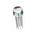
| 描述 | IC CONV TRUE RMS/DC TO-100-10专业电源管理 RMS/DC CONVERTER IC |
| 产品分类 | |
| 品牌 | Analog Devices Inc |
| 产品手册 | |
| 产品图片 |
|
| rohs | 符合RoHS无铅 / 符合限制有害物质指令(RoHS)规范要求 |
| 产品系列 | 电源管理 IC,专业电源管理,Analog Devices AD536AKHZ- |
| 数据手册 | |
| 产品型号 | AD536AKHZ |
| 产品培训模块 | http://www.digikey.cn/PTM/IndividualPTM.page?site=cn&lang=zhs&ptm=25912 |
| 产品种类 | 专业电源管理 |
| 供应商器件封装 | TO-100-10 |
| 功率耗散 | 500 mW |
| 包装 | 管件 |
| 商标 | Analog Devices |
| 安装类型 | 通孔 |
| 安装风格 | Through Hole |
| 封装 | Bulk |
| 封装/外壳 | TO-100-10 金属罐 |
| 封装/箱体 | TO-100-10 |
| 工作温度范围 | 0 C to + 70 C |
| 工厂包装数量 | 100 |
| 标准包装 | 1 |
| 电压-电源 | 5.0V ~ 36V, ±3.0V ~ 18V |
| 电流-电源 | 1.2mA |
| 电源电压 | 15 V |
| 电源电流 | 1 mA |
| 类型 | RMS to DC Converter |
| 系列 | AD536A |


- 商务部:美国ITC正式对集成电路等产品启动337调查
- 曝三星4nm工艺存在良率问题 高通将骁龙8 Gen1或转产台积电
- 太阳诱电将投资9.5亿元在常州建新厂生产MLCC 预计2023年完工
- 英特尔发布欧洲新工厂建设计划 深化IDM 2.0 战略
- 台积电先进制程称霸业界 有大客户加持明年业绩稳了
- 达到5530亿美元!SIA预计今年全球半导体销售额将创下新高
- 英特尔拟将自动驾驶子公司Mobileye上市 估值或超500亿美元
- 三星加码芯片和SET,合并消费电子和移动部门,撤换高东真等 CEO
- 三星电子宣布重大人事变动 还合并消费电子和移动部门
- 海关总署:前11个月进口集成电路产品价值2.52万亿元 增长14.8%

PDF Datasheet 数据手册内容提取
Integrated Circuit True RMS-to-DC Converter Data Sheet AD536A FEATURES FUNCTIONAL BLOCK DIAGRAM True rms-to-dc conversion AD536A Laser trimmed to high accuracy ABSOLUTE ±0.2% maximum error (AD536AK) VIN VALUE ±0.5% maximum error (AD536AJ) Wide response capability SQUARER/ dB Computes rms of ac and dc signals COM DIVIDER 450 kHz bandwidth: V rms > 100 mV +VS + 2 MHz bandwidth: V rms > 1 V CAV Signal crest factor of 7 for 1% error CURRENT MIRROR dB output with 60 dB range Low power: 1.2 mA quiescent current 25kΩ RL Single- or dual-supply operation IOUT Monolithic integrated circuit +VS −55°C to +125°C operation (AD536AS) BUFFER IN BUF 25kΩ GENERAL DESCRIPTION BUFFER pTehref oArDm5s 3t6ruAe irsm a sc-otom-pdlce tceo nmvoenrsoiloitnh. iIct ionftfeegrsr apteerdf ocrirmcuaintc teh at 80kΩ–VS OUT 00504-001 comparable or superior to that of hybrid or modular units costing Figure 1. much more. The AD536A directly computes the true rms value of The AD536A is available in two accuracy grades (J and K) for any complex input waveform containing ac and dc components. commercial temperature range (0°C to 70°C) applications, and A crest factor compensation scheme allows measurements with 1% one grade (S) rated for the −55°C to +125°C extended range. error at crest factors up to 7. The wide bandwidth of the device The AD536AK offers a maximum total error of ±2 mV ± 0.2% extends the measurement capability to 300 kHz with less than 3 dB of reading, while the AD536AJ and AD536AS have maximum errors for signal levels greater than 100 mV. errors of ±5 mV ± 0.5% of reading. All three versions are available An important feature of the AD536A, not previously available in a hermetically sealed 14-lead DIP or a 10-pin TO-100 metal in rms converters, is an auxiliary dB output pin. The logarithm header package. The AD536AS is also available in a 20-terminal of the rms output signal is brought out to a separate pin to allow leadless hermetically sealed ceramic chip carrier. the dB conversion, with a useful dynamic range of 60 dB. Using The AD536A computes the true root-mean-square level of a an externally supplied reference current, the 0 dB level can be complex ac (or ac plus dc) input signal and provides an equiva- conveniently set to correspond to any input level from 0.1 V to lent dc output level. The true rms value of a waveform is a more 2 V rms. useful quantity than the average rectified value because it relates The AD536A is laser trimmed to minimize input and output offset directly to the power of the signal. The rms value of a statistical voltage, to optimize positive and negative waveform symmetry signal also relates to its standard deviation. (dc reversal error), and to provide full-scale accuracy at 7 V rms. An external capacitor is required to perform measurements to the As a result, no external trims are required to achieve the rated fully specified accuracy. The value of this capacitor determines the unit accuracy. low frequency ac accuracy, ripple amplitude, and settling time. The input and output pins are fully protected. The input circuitry The AD536A operates equally well from split supplies or a can take overload voltages well beyond the supply levels. Loss of single supply with total supply levels from 5 V to 36 V. With supply voltage with the input connected to external circuitry does 1 mA quiescent supply current, the device is well suited for a not cause the device to fail. The output is short-circuit protected. wide variety of remote controllers and battery-powered instruments. Rev. F Document Feedback Information furnished by Analog Devices is believed to be accurate and reliable. However, no responsibility is assumed by Analog Devices for its use, nor for any infringements of patents or other One Technology Way, P.O. Box 9106, Norwood, MA 02062-9106, U.S.A. rights of third parties that may result from its use. Specifications subject to change without notice. No license is granted by implication or otherwise under any patent or patent rights of Analog Devices. Tel: 781.329.4700 ©1976–2014 Analog Devices, Inc. All rights reserved. Trademarks and registered trademarks are the property of their respective owners. Technical Support www.analog.com
AD536A Data Sheet TABLE OF CONTENTS Features .............................................................................................. 1 Frequency Response .....................................................................9 General Description ......................................................................... 1 AC Measurement Accuracy and Crest Factor ...........................9 Functional Block Diagram .............................................................. 1 Applications Information .............................................................. 11 Revision History ............................................................................... 2 Typical Connections .................................................................. 11 Specifications ..................................................................................... 3 Optional External Trims For High Accuracy ......................... 11 Absolute Maximum Ratings ............................................................ 5 Single-Supply Operation ........................................................... 12 ESD Caution .................................................................................. 5 Choosing the Averaging Time Constant ................................. 12 Pin Configurations and Function Descriptions ........................... 6 Outline Dimensions ....................................................................... 14 Theory of Operation ........................................................................ 8 Ordering Guide .......................................................................... 15 Connections for dB Operation ................................................... 8 REVISION HISTORY 11/14—Rev. E to Rev. F Changes to Connections for dB Operation Section .................. 11 Change to Figure 1 ........................................................................... 1 Changes to Figure 17 ...................................................................... 12 Changes to Table 1 ............................................................................ 3 Changes to Frequency Response Section .................................... 12 Change to Figure 16 ....................................................................... 12 Updated Outline Dimensions ....................................................... 14 Changes to Ordering Guide .......................................................... 15 Changes to Ordering Guide .......................................................... 15 7/12—Rev. D to Rev. E 3/06—Rev. B to Rev. C Reorganized Layout ............................................................ Universal Updated Format .................................................................. Universal Changes to Figure 1 .......................................................................... 1 Changed Product Description to General Description ................ 1 Changes to Figure 6 .......................................................................... 8 Changes to General Description ..................................................... 1 Changes to Figure 7 .......................................................................... 9 Changes to Table 1 ............................................................................. 3 Changes to Figure 13, Figure 14, and Figure 15 ......................... 11 Changes to Table 2 ............................................................................. 5 Changes to Figure 16, Figure 17, and Single-Supply Operation Added Pin Configurations and Function Descriptions ............... 6 Section .............................................................................................. 12 Changed Standard Connection to Typical Connections ............. 8 Changes to Figure 21 ...................................................................... 13 Changed Single Supply Connection to Single Supply Updated Outline Dimensions ....................................................... 14 Operation ............................................................................................ 9 Changes to Connections for dB Operation................................. 11 8/08—Rev. C to Rev. D Changes to Figure 17 ...................................................................... 12 Changes to Features Section............................................................ 1 Updated Outline Dimensions ....................................................... 14 Changes to General Description Section ...................................... 1 Changes to Ordering Guide .......................................................... 15 Changes to Figure 1 .......................................................................... 1 Changes to Table 2 ............................................................................ 5 6/99—Rev. A to Rev. B Change to Figure 2 ........................................................................... 5 Changes to Figure 15 ...................................................................... 10 1/76—Revision 0: Initial Version Rev. F | Page 2 of 15
Data Sheet AD536A SPECIFICATIONS T = +25°C and ±15 V dc, unless otherwise noted. A Table 1. AD536AJ AD536AK AD536AS Parameter Min Typ Max Min Typ Max Min Typ Max Unit TRANSFER FUNCTION VOUT = √Avg(VIN)2 VOUT = √Avg(VIN)2 VOUT = √Avg(VIN)2 CONVERSION ACCURACY Total Error, Internal Trim1 ±5 ± 0.5 ±2 ± 0.2 ±5 ± 0.5 mV ± % of rdg (See Figure 13) vs. Temperature TMIN to +70°C ±0.1 ± 0.01 ±0.05 ± ±0.1 ± mV ± % of rdg/°C 0.005 0.005 +70°C to +125°C ±0.3 ± mV ± % of rdg/°C 0.005 vs. Supply Voltage ±0.1 ± 0.01 ±0.1 ± 0.01 ±0.1 ± 0.01 mV ± % of rdg/V DC Reversal Error ±0.2 ±0.1 ±0.2 mV ± % of rdg Total Error, External Trim1 ±3 ± 0.3 ±2 ± 0.1 ±3 ± 0.3 mV ± % of rdg (See Figure 16) ERROR VS. CREST FACTOR2 Crest Factor 1 to Crest Factor 2 Specified accuracy Specified accuracy Specified accuracy Crest Factor = 3 −0.1 −0.1 −0.1 % of rdg Crest Factor = 7 −1.0 −1.0 −1.0 % of rdg FREQUENCY RESPONSE3 Bandwidth for 1% Additional Error (0.09 dB) VIN = 10 mV 5 5 5 kHz VIN = 100 mV 45 45 45 kHz VIN = 1 V 120 120 120 kHz ±3 dB Bandwidth VIN = 10 mV 90 90 90 kHz VIN = 100 mV 450 450 450 kHz VIN = 1 V 2.3 2.3 2.3 MHz AVERAGING TIME CONSTANT 25 25 25 ms/µF (See Figure 19) INPUT CHARACTERISTICS Signal Range, ±15 V Supplies Continuous RMS Level 0 to 7 0 to 7 0 to 7 V rms Peak Transient Input ±20 ±20 ±20 V peak Continuous RMS Level, 0 to 2 0 to 2 0 to 2 V rms VS = ±5 V Peak Transient Input, ±7 ±7 ±7 V peak VS = ±5 V Maximum Continuous ±25 ±25 ±25 V peak Nondestructive Input Level (All Supply Voltages) Input Resistance 13.33 16.67 20 13.33 16.67 20 13.33 16.67 20 kΩ Input Offset Voltage 0.8 ±2 0.5 ±1 0.8 ±2 mV OUTPUT CHARACTERISTICS Offset Voltage, VIN = COM ±1 ±2 ±0.5 ±1 ±2 mV (See Figure 13) vs. Temperature ±0.1 ±0.1 ±0.2 mV/°C vs. Supply Voltage ±0.1 ±0.1 ±0.2 mV/V Voltage Swing, ±15 V Supplies 0 to +11 +12.5 0 to +11 +12.5 0 to +11 +12.5 V ± 5 V Supply 0 to +2 0 to +2 0 to +2 V dB OUTPUT, 0 dB = 1 V rms (See Figure 7) Error, 7 mV < VIN < 7 V rms ±0.4 ±0.6 ±0.2 ±0.3 ±0.5 ±0.6 dB Scale Factor −3 −3 −3 mV/dB Scale Factor Temperature −0.033 −0.033 −0.033 dB/°C Coefficient Uncompensated +0.33 +0.33 +0.33 % of rdg/°C IREF for 0 dB = 1 V rms 5 20 80 5 20 80 5 20 80 µA IREF Range 1 100 1 100 1 100 µA Rev. F | Page 3 of 15
AD536A Data Sheet AD536AJ AD536AK AD536AS Parameter Min Typ Max Min Typ Max Min Typ Max Unit IOUT TERMINAL IOUT Scale Factor 40 40 40 µA/V rms IOUT Scale Factor Tolerance ±10 ±20 ±10 ±20 ±10 ±20 % Output Resistance 20 25 30 20 25 30 20 25 30 kΩ Voltage Compliance −VS to −VS to −VS to V (+VS − 2.5 V) (+VS − 2.5 V) (+VS − 2.5 V) BUFFER AMPLIFIER Input and Output Voltage −VS to −VS to −VS to V Range (+VS − 2.5V) (+VS − 2.5V) (+VS − 2.5V) Input Offset Voltage, RS = 25 kΩ ±0.5 ±4 ±0.5 ±4 ±0.5 ±4 mV Input Bias Current 20 60 20 60 20 60 nA Input Resistance 108 108 108 Ω Output Current (+5 mA, (+5 mA, (+5 mA, −130 µA) −130 µA) −130 µA) Short-Circuit Current 20 20 20 mA Output Resistance 0.5 0.5 0.5 Ω Small-Signal Bandwidth 1 1 1 MHz Slew Rate4 5 5 5 V/µs POWER SUPPLY Voltage Rated Performance ±15 ±15 ±15 V Dual Supply ±3.0 ±18 ±3.0 ±18 ±3.0 ±18 V Single Supply +5 +36 +5 +36 +5 +36 V Quiescent Current Total VS, 5 V to 36 V, TMIN to TMAX 1.2 2 1.2 2 1.2 2 mA TEMPERATURE RANGE Rated Performance 0 +70 0 +70 −55 +125 °C Storage −55 +150 −55 +150 −55 +150 °C NUMBER OF TRANSISTORS 65 65 65 1 Accuracy is specified for 0 V to 7 V rms, dc or 1 kHz sine wave input with the AD536A connected as in the figure referenced. 2 Error vs. crest factor is specified as an additional error for 1 V rms rectangular pulse input, pulse width = 200 μs. 3 Input voltages are expressed in volts rms, and error is expressed as a percentage of the reading. 4 With 2 kΩ external pull-down resistor. Rev. F | Page 4 of 15
Data Sheet AD536A ABSOLUTE MAXIMUM RATINGS Stresses at or above those listed under Absolute Maximum Table 2. Ratings may cause permanent damage to the product. This is a Parameter Rating stress rating only; functional operation of the product at these Supply Voltage or any other conditions above those indicated in the operational Dual Supply ±18 V section of this specification is not implied. Operation beyond Single Supply +36 V the maximum operating conditions for extended periods may Internal Power Dissipation 500 mW affect product reliability. Maximum Input Voltage ±25 V peak ESD CAUTION Buffer Maximum Input Voltage ±V S Maximum Input Voltage ±25 V peak Storage Temperature Range −55°C to +150°C Operating Temperature Range AD536AJ/AD536AK 0°C to +70°C AD536AS −55°C to +125°C Lead Temperature (Soldering, 60 sec) 300°C ESD Rating 1000 V Thermal Resistance θ 1 JA 10-Pin Header (H-10 Package) 150°C/W 20-Terminal LCC (E-20 Package) 95°C/W 14-Lead SBDIP (D-14 Package) 95°C/W 14-Lead CERDIP (Q-14 Package) 95°C/W 1 θJA is specified for the worst-case conditions, that is, a device soldered in a circuit board for surface-mount packages. 0.1315 (3.340) +VS COM RL 14 10 9 IOUT 8 0.0807 (2.050) VIN 1A1 BUF IN VIN 7 1B1 –VS CAVdB BUF OUT 3 4 5 6 PAD NUMBERS CORRESPOND TO PIN NUMBERS FOR THE TO-100 14-LEAD CERAMIC DIP PACKAGE. 1BOTH PADS SHOWN MUST BE CONNECTED TO VIN. TSHUEB SATDR5A3T6AE ICSO ANVNAEICLATEBDLE T OIN –LVASS.ER-TRIMMED CHIP FORM. 00504-002 Figure 2. Die Dimensions and Pad Layout Dimensions shown in inches and (millimeters) Rev. F | Page 5 of 15
AD536A Data Sheet PIN CONFIGURATIONS AND FUNCTION DESCRIPTIONS VIN 1 14 +VS NC 2 13 NC –VS 3 AD536A 12 NC CAV 4 TOP VIEW 11 NC (Not to Scale) dB 5 10 COM BUF OUT 6 9 RL BUF IN 7NC = NO CONNECT8 IOUT 00504-003 Figure 3. D-14 and Q-14 Packages Pin Configuration Table 3. D-14 and Q-14 Packages Pin Function Descriptions Pin No. Mnemonic Description 1 V Input Voltage IN 2 NC No Connection 3 −V Negative Supply Voltage S 4 C Averaging Capacitor AV 5 dB Log (dB) Value of the RMS Output Voltage 6 BUF OUT Buffer Output 7 BUF IN Buffer Input 8 I RMS Output Current OUT 9 R Load Resistor L 10 COM Common 11 NC No Connection 12 NC No Connection 13 NC No Connection 14 +V Positive Supply Voltage S IOUT RL 10 BUF IN 1 9 COM 2 AD536A 8 BUF OUT TOP VIEW (Not to Scale) +VS 3 7 dB VIN4 –V5S 6CAV 00504-004 Figure 4. H-10 Package Pin Configuration Table 4. H-10 Package Pin Function Descriptions Pin No. Mnemonic Description 1 R Load Resistor L 2 COM Common 3 +V Positive Supply Voltage S 4 V Input Voltage IN 5 −V Negative Supply Voltage S 6 C Averaging Capacitor AV 7 dB Log (dB) Value of the RMS Output Voltage 8 BUF OUT Buffer Output 9 BUF IN Buffer Input 10 I RMS Output Current OUT Rev. F | Page 6 of 15
Data Sheet AD536A NC VIN NC +VS NC 3 2 1 20 19 –VS 4 18 NC NC 5 AD536A 17 NC CAV 6 TOP VIEW 16 NC (Not to Scale) NC 7 15 NC dB 8 14 COM 9 10 11 12 13 NCBUF OUT = NBUF INO CNCONINOUTECRTL 00504-005 Figure 5. E-20 Package Pin Configuration Table 5. E-20 Package Pin Function Descriptions Pin No. Mnemonic Description 1 NC No Connection 2 V Input Voltage IN 3 NC No Connection 4 −V Negative Supply Voltage S 5 NC No Connection 6 C Averaging Capacitor AV 7 NC No Connection 8 dB Log (dB) Value of the RMS Output Voltage 9 BUF OUT Buffer Output 10 BUF IN Buffer Input 11 NC No Connection 12 I RMS Output Current OUT 13 R Load Resistor L 14 COM Common 15 NC No Connection 16 NC No Connection 17 NC No Connection 18 NC No Connection 19 NC No Connection 20 +V Positive Supply Voltage S Rev. F | Page 7 of 15
AD536A Data Sheet THEORY OF OPERATION The AD536A embodies an implicit solution of the rms equation The current mirror also produces the output current, I , which OUT that overcomes the dynamic range as well as other limitations equals 2I. I can be used directly or can be converted to a 4 OUT inherent in a straightforward computation of rms. The actual voltage with R2 and buffered by A4 to provide a low impedance computation performed by the AD536A follows the equation voltage output. The transfer function of the AD536A results in the following: V 2 Vrms=Avg IN V = 2R2 × I rms = V rms Vrms OUT IN The dB output is derived from the emitter of Q3 because the Figure 6 is a simplified schematic of the AD536A. Note that it is voltage at this point is proportional to –log V . The emitter IN subdivided into four major sections: absolute value circuit follower, Q5, buffers and level shifts this voltage so that the dB (active rectifier), squarer/divider, current mirror, and buffer output voltage is zero when the externally supplied emitter amplifier. The input voltage (V ), which can be ac or dc, is IN current (I ) to Q5 approximates I. REF 3 converted to a unipolar current (I) by the active rectifiers 1 CONNECTIONS FOR dB OPERATION (A, A). I drives one input of the squarer/divider, which has 1 2 1 the transfer function The logarithmic (or decibel) output of the AD536A is one of I = I2/I its most powerful features. The internal circuit computing dB 4 I 3 works accurately over a 60 dB range. The connections for dB The output current, I, of the squarer/divider drives the current 4 measurements are shown in Figure 7. mirror through a low-pass filter formed by R1 and the exter- Select the 0 dB level by adjusting R1 for the proper 0 dB reference nally connected capacitor, C . If the R1 C time constant is AV AV current (which is set to cancel the log output current from the much greater than the longest period of the input signal, then squarer/divider at the desired 0 dB point). The external op amp I is effectively averaged. The current mirror returns a current 4 provides a more convenient scale and allows compensation of I, which equals Avg[I], back to the squarer/divider to complete 3 4 the +0.33%/°C scale factor drift of the dB output pin. the implicit rms computation. Thus, I = Avg[I2/I] = I rms The temperature-compensating resistor, R2, is available online 4 I 4 I in several styles from Precision Resistor Company, Inc., (Part CURRENT MIRROR Number AT35 and Part Number ST35). The average temperature 14 +VS coefficients of R2 and R3 result in the +3300 ppm required to 10 compensate for the dB output. The linear rms output is available COM R1 0.4mA at Pin 8 on the DIP or Pin 10 on the header device with an output ABSOLUTEVALUE; 0.2mFAS I3 25kΩ FS impedance of 25 kΩ. Some applications require an additional VOLTAGE-CURRENT 4 8 9 CONVERTER A3 I2 IOUT 25Rk2Ω RL buffer amplifier if this output is desired. V1IN 50Rk4Ω |VIN|R–1 I1 Q1 Q3 I7NBUBFAU4FFER Od5UBT F1.o r dSBe tc ValIiNb r=a t1i.o0n0, V dc or 1.00 V rms. A1 Q2 Q4 Q5 2. Adjust R1 for dB output = 0.00 V. 6 12kΩ A2 25kΩ BUF 3. Set VIN = +0.1 V dc or 0.10 V rms. R3 12kΩ ONE-QUADRANT 80kΩ OUT 4. Adjust R5 for dB output = −2.00 V. 25kΩ SQUARER/DIVIDER N1.O PTINESOUTSARE FOR 14-LEAD DIP. –V3S 00504-106 AVnINy a ontdh eard jduesstiirnegd R01 d aBc croefredrienngcley. lNevoetle c tahna tb ae dujsuesdti nbgy Rse5t tfionrg the Figure 6. Simplified Schematic proper gain automatically provides the correct temperature compensation. Rev. F | Page 8 of 15
Data Sheet AD536A VIN 1 ABVSAOLLUUETE 14 +VS +4.V6SV TO 18V +E NC 2 AD536A 13 NC –VS –VS 3 SDQIUVAIDREERR/ 12 NC EOUT AD580J +VS C+1, CAV CAV 4 11 NC 2.5V R4 FACdTBO SRC AADLJEUST 0.C12µF BUF OUdBT 56 CMUIRRRREONRT 190 CROLM 0dB500kRΩ1 –E 33.2kΩ +VS 5Rk5Ω d3mB VO/dUBT BUF IN 7 BUF 25kΩ 8 IOUT LRAINDEFEJUASRT R246.9kΩ R603.4Ω 2 OP777 6 TEMPERATURE rOmUsTPUT R21 3 4 CdBO MOPUETNPSUATTED 1kΩ +100mV/dB –VS 1 SPPREECCIIASLIO TNC R CEOSMISPTEONRS ACTOIMOPNA RNEYS PISATROTR N, U+3M3B00EpRp AmT/° 3C5, OR PART NUMBER ST35. 00504-107 Figure 7. dB Connection FREQUENCY RESPONSE Figure 9 illustrates a curve of reading error for the AD536A for a 1 V rms input signal with crest factors from 1 to 11. A rectan- The AD536A utilizes a logarithmic circuit in performing the gular pulse train (pulse width = 100 μs) was used for this test implicit rms computation. As with any log circuit, bandwidth because it is the worst-case waveform for rms measurement (all is proportional to signal level. The solid lines in the graph of of the energy is contained in the peaks). The duty cycle and Figure 8 represent the frequency response of the AD536A at peak amplitude were varied to produce crest factors from 1 to input levels from 10 mV rms to 7 V rms. The dashed lines indicate 11 while maintaining a constant 1 V rms input amplitude. the upper frequency limits for 1%, 10%, and ±3 dB of reading additional error. For example, note that a 1 V rms signal produces T өO less than 1% of reading additional error up to 120 kHz. A 10 mV 100µs signal can be measured with 1% of reading additional error 0 VP ηC F= =D 1U/T√Yη CYCLE = T (100 μV) up to only 5 kHz. өIN (rms) = 1 V rms 100µs 1 10 g) n 7Vrms INPUT 1% di 10% ea 0 R (V)UT 1 1Vrms INPUT ±3dB R (% of –1 VO0.1 RRO 100mVrms INPUT E E IN –2 S 0.01 A E 10mVrms INPUT R NC–3 I 1k Fig1u0kre 8. HFiRgEhQ FUr1eE0qN0ukCeYn(cHyz R)espo1nMse 10M 00504-016 –41 2 3 4 C5REST 6FACTO7R 8 9 10 11 00504-017 Figure 9. Error vs. Crest Factor AC MEASUREMENT ACCURACY AND CREST FACTOR R Crest factor is often overlooked when determining the accuracy ROG) of an ac measurement. The definition of crest factor is the ratio N ERADIN10 1VrmsCF=10 of the peak signal amplitude to the rms value of the signal E IRE (CF = VP/V rms). Most common waveforms, such as sine and REAS% OF 1 triangle waves, have relatively low crest factors (<2). Waveforms NC( 1VrmsCF=3 I that resemble low duty cycle pulse trains, such as those occurring 0.1 ifnac stworistc. hFionrg e pxoamweprl es,u ap rpelcietsa nagnudl aSrC pRu clsierc turaitisn, hwaivthe ha i1g%h cdruetsyt 1µs PU10LµSsEWID1T0H0µ(µss) 1000µs 00504-018 cycle has a crest factor of 10 (CF = 1√n). Figure 10. Error vs. Pulse Width Rectangular Pulse Rev. F | Page 9 of 15
AD536A Data Sheet 25 25 T OR OUTPUT (V) 2105 VIN UT OR OUTPUT (V) 2105 VIN VOUT K INPU 10 VOUT AK INP 10 EA PE ±P 5 ± 5 2.5 0 Figure 11. In±p6uVtO aLnTSd O(DuUtApLu± St1 UV0PoPltLaYg)e Rang±e1s6 vs. ±18 00504-019 0 Figu5re 12. In1p0VuOtL aTnSd ( SOINuGtpLuE2t 0SVUoPltPaLgYe) Range3s0 vs. 00504-022 Dual Supply Single Supply Rev. F | Page 10 of 15
Data Sheet AD536A APPLICATIONS INFORMATION TYPICAL CONNECTIONS CAV VIN +VS NC NC NC The AD536A is simple to connect to for the majority of high 3 2 1 20 19 accuracy rms measurements, requiring only an external capaci- –VS –VS 4 ABVSAOLLUUETE 18 NC tor to set the averaging time constant. The standard connection AD536A is shown in Figure 13 through Figure 15. In this configuration, CNACV 5 SDQIUVAIDREERR/ 17 NC 6 16 NC the AD536A measures the rms of the ac and dc levels present at the input, but shows an error for low frequency input as a function NC 7 CMUIRRRREONRT 15 NC of the filter capacitor, C , as shown in Figure 19. Thus, if a 4 µF dB 8 BUF 25kΩ 14 COM AV capacitor is used, the additional average error at 10 Hz is 0.1%; 9 10 11 12 13 aTTtoh 3 er eHajcezcc, utt hrtahece ay dd acdt i ihtniiopgnuhate,l r aa fdvrdeerq aau gceean pecarirecosit roi sir s a i1cnc% soe.r r diiensg w tioth s pthecei finicpautito, n. VOUT BUF OUT BUF IN NC IOUT RL 00504-021 Figure 15. 20-Terminal Standard RMS Connection as shown in Figure 17. Note that the capacitor must be nonpolar. If the AD536A supply rails contain a considerable amount of The input and output signal ranges are a function of the supply high frequency ripple, it is advisable to bypass both supply pins voltages; these ranges are shown in Figure 11 and Figure 12. to ground with 0.1 µF ceramic capacitors, located as close to the The AD536A can also be used in an unbuffered voltage output device as possible. mode by disconnecting the input to the buffer. The output then CAV appears unbuffered across the 25 kΩ resistor. The buffer ampli- fier can then be used for other purposes. Further, the AD536A AD536A VIN VIN 1 ABVSAOLLUUETE 14+VS +VS c2a5n k bΩe ruesseisdt oinr far ocmur rgernotu onudt.p Tuht em ooudtep ubty c duirsrceonntn ies catvinaigl atbhlee at NC 2 13 NC Pin 8 (I , Pin 10 on the H-10 package) with a nominal scale of –VS –VS 3 SDQIUVAIDREERR/ 12 NC 40 μA pOeUrT V rms input positive output. CAV 4 11 NCCOM OPTIONAL EXTERNAL TRIMS FOR HIGH dB 5 CURRENT 10 BUF OUT MIRROR ACCURACY VOUTBUF IN 67 BUF 25kΩ 98 RL The accuracy and offset voltage of the AD536A is adjustable IOUT 00504-006 wNiotthe etxhtaetr tnhael otrfifmsest, tarsim sh coiwrcnu iitn a Fdidgsu 3re6 51 6Ω. Rin4 streirmiess twhiet ho ftfhsee t. Figure 13. 14-Lead Standard RMS Connection internal 25 kΩ resistor. This causes a 1.5% increase in scale factor, IOUT which is compensated for by R1. The scale factor adjustment RL BUF IN range is ±1.5%. 25kΩ The trimming procedure is as follows: AD536A BUF OUT COM CURRENT BUF VOUT 1. Ground the input signal, VIN, and adjust R4 to provide 0 V MIRROR output from Pin 6. Alternatively, adjust R4 to provide the +VS +VS SDQIUVAIDREERR/ dB correct output with the lowest expected value of VIN. 2. Connect the desired full-scale input level to V , either dc ABSOLUTE IN VIN VALUE CAV or a calibrated ac signal (1 kHz is the optimum frequency). CAV –VS 00504-020 3. T1.r0im00 R V1 dtoc pinropvuitd pe rtohve icdoersr e1c.0t 0o0u tVpu dt ca to Puitnp u6t. .F Aor ± e1x.a0m00p lVe, peak-to-peak sine wave should provide a 0.707 V dc output. Figure 14. 10-Pin Standard RMS Connection Any residual errors are caused by device nonlinearity. The major advantage of external trimming is to optimize device performance for a reduced signal range; the AD536A is internally trimmed for a 7 V rms full-scale range. Rev. F | Page 11 of 15
AD536A Data Sheet CAV CHOOSING THE AVERAGING TIME CONSTANT SCALE FACTOR ADJUST The AD536A computes the rms of both ac and dc signals. If the VIN 1 ABVSAOLLUUETE 14 +VS +VS input is a slowly varying dc signal, the output of the AD536A R1 tracks the input exactly. 500kΩ NC 2 AD536A 13 NC +VS –VS –VS 3 SDQIUVAIDREERR/ 12 NC R504kΩ OADFJFUSSETT Aaptp hriogahcehre fsr ethqeu ernmcsi evsa, ltuhee oafv tehrea gien pouutt psiugtn oafl .t hTeh Ae aDc5tu3a6lA o utput CAV 4 11 NC –VS of the AD536A differs from the ideal output by a dc (or average) dB 5 CMUIRRRREONRT 10 COM R7530kΩ error and some amount of ripple, as shown in Figure 18. VOUT BUF OUT 6 9 EO 25kΩ RL R2 BUF IN 7 BUF 8 365kΩ 25kΩ IOUT IDEAL EO 00504-007 DC ERROR = EO – EO (IDEAL) Figure 16. Optional External Gain and Output Offset Trims SINGLE-SUPPLY OPERATION AVERAGE EO – EO DOUBLE FREQUENCY R5 eVfe arn tdo 3F6ig Vu.r eW 1h7e fno rp soiwngerlee dsu fpropmly -ar asiiln cgolen fsiugpupralyt,i othnes ibneptwute en RIPPLE TIME 00504-009 stage (VIN pin) is internally biased at a voltage between ground Figure 18. Typical Output Waveform for Sinusoidal Input and the supply, and the input signal ac coupled. Biasing the The dc error is dependent on the input signal frequency and device between the supply and ground is simply a matter of the value of C . Use Figure 19 to determine the minimum value AV connecting the COM pin to an external resistor divider and of C , which yields a given percentage of dc error above a given AV bypassing to ground. The resistor values are large, minimizing frequency using the standard rms connection. power consumption, as the COM pin current is only 5 μA. The ac component of the output signal is the ripple. There are Note that the 10 kΩ and 20 kΩ resistors connected to the COM pin two ways to reduce the ripple. The first method involves using a (Figure 17) are asymmetrical, that is, the voltage at the COM pin is large value of C . Because the ripple is inversely proportional AV 1/3 of the supply. This ratio of input bias to supply is optimum to C , a tenfold increase in this capacitance affects a tenfold AV for the precision rectifier (aka absolute value circuit) input reduction in ripple. circuit employed for rectifying ac input waveforms and ensures When measuring waveforms with high crest factors, such as low full input symmetry for low signal voltages. duty cycle pulse trains, the averaging time constant should be at Capacitor C2 is required for AC input coupling, however an least 10 times the signal period. For example, a 100 Hz pulse external dc return is unnecessary because biasing occurs rate requires a 100 ms time constant, which corresponds to a internally. SelectC2 for the desired low frequency breakpoint 4 μF capacitor (time constant = 25 ms per μF). using an input resistance of 16.7 kΩ for the 1/ωRC calculation; C2 = 1 μF for a cutoff at 10 Hz. Figure 11 and Figure 12 show the input and output signal ranges for dual and single supply configurations, respectively. The load resistor, RL, provides a path to sink output sink current when an input signal is disconnected. CAV C2 1µF VIN VIN 1 ABVSAOLLUUETE 14 +VS +VS 0.1µF NONPOLARIZED NC 2 AD536A 13 NC –VS 3 SDQIUVAIDREERR/ 12 NC 20kΩ 4 11 NC CAV dB 5 CURRENT 10 COM VOUT BUF OUT MIRROR RL 0.1µF 6 9 25kΩ RL 11T0kkOΩΩBUF IN 7 BUF 8 IOUT 10kΩ 00504-008 Figure 17. Single-Supply Connection Rev. F | Page 12 of 15
Data Sheet AD536A The primary disadvantage in using a large C to remove ripple The settling time, however, is increased by approximately a AV is that the settling time for a step change in input level is factor of 3. Therefore, the values of C and C2 can be reduced AV increased proportionately. Figure 19 illustrates that the to permit faster settling times while still providing substantial relationship between C and 1% settling time is 115 ms for ripple reduction. AV each microfarad of C . The settling time is twice as great for AV The two-pole postfilter uses an active filter stage to provide decreasing signals as it is for increasing signals. The values in even greater ripple reduction without substantially increasing Figure 19 are for decreasing signals. Settling time also increases the settling times over a circuit with a one-pole filter. The values for low signal levels, as shown in Figure 20. of C , C2, and C3 can then be reduced to allow extremely fast AV 100 100 settling times for a constant amount of ripple. Caution should be exercised in choosing the value of C , because the dc error 0.01 NDS is dependent on this value and is indepAeVndent of the postfilter. REQUIRED C (µF)AV01.011 V1FA%OAVLER SUR SEEATTSGAT LIFTNIOENGDRG E % CTRAI RMOVO FEA RRN110ED%A EDRIRNO1G%R ERRO0.R1% ERROR% ERROR 011.01 OR 1% SETTLING TIME IN SECOMULTIPLY READING BY 0.115 FDoCr Ca omnovre–erVV sIdNSioent–aVN VAiICNlSepdp123 leicxaAptDliao5nn3AaS G6tBDQViASIouUAVOnAiILDdLRU EoeUEE,RfTR 2Et/hneds eE 111dto243itpii+NNocVCCnsS,. r+eVfeSr to the RMS to ACCURACY ± 20% DUE TO F CAV COMPONENT TOLERANCE 4 11 NC 0.011 10 INPUT1 0F0REQUENC1Yk (Hz) 10k 1000k.01 00504-010 CABVUF OdUBT 56 CMUIRRRREONRT 190 CROLM 1PERCENT DC ERROR AND PERCENT RIPPLE (PEAK) BUF IN 25kΩ IOUT 7 BUF 8 Figure 19. Error/Settling Time Graph for Use with the Standard RMS Connection (See Figure 13 Through Figure 15) + Rx – s –C2 24kΩ C31 + m TO 1V rME10.0 1FOR SINGLE POLE, SHORT Rx, REMOVE C3. Vrms OUT 00504-012 ETI LATIVLING 7.5 Figure 21. Two-Pole Postfilter ET RT ETTLING TIME INPUT SE52..05 % of Reading)10 PEAK-TO-PEAK PCEAVA K= -1TµOF-PEAK RIPPLE S 1.0 LE ( RCIAPVP =L E1µ (FO,N CE2 P=O 2L.2Eµ)F P 1m 10m rms INP1U0T0 mLEVEL (V) 1 10 00504-011 R OR RIP 1 DC(ACALRV LEx = R F= 1RI L0µOTΩFRERS) Figure 20. Settling Time vs. Input Level RO ER PEAK-TO-PEAK RIPPLE A better method to reduce output ripple is the use of a postfilter. C CAV = 1µF D C2 = C3 = 2.2µF (TWO-POLE) Figure 21 shows a suggested circuit. If a single-pole filter is used (C3 removed, RX shorted) and C2 is approximately twice the 0.110 100 1k 10k 00504-013 value of C , the ripple is reduced, as shown in Figure 22, and AV FREQUENCY (Hz) settling time is increased. For example, with C = 1 µF and C2 AV Figure 22. Performance Features of Various Filter Types = 2.2 μF, the ripple for a 60 Hz input is reduced from 10% of (See Figure 13 to Figure 15 for Standard RMS Connection) reading to approximately 0.3% of reading. Rev. F | Page 13 of 15
AD536A Data Sheet OUTLINE DIMENSIONS 0.005 (0.13) MIN 0.080 (2.03) MAX 14 8 0.310 (7.87) 1 0.220 (5.59) 7 PIN 1 0.100 (2.54) BSC 0.320 (8.13) 0.765 (19.43) MAX 0.290 (7.37) 0.200 (5.08) 0.060 (1.52) MAX 0.015 (0.38) 0.150 (3.81) 0.200 (5.08) MIN 0.125 (3.18) 0.070 (1.78) SPELAANTIENG 00..001058 ((00..3280)) 0.023 (0.58) 0.030 (0.76) 0.014 (0.36) CONTROLLING DIMENSIONS ARE IN INCHES; MILLIMETER DIMENSIONS (IN PARENTHESES) ARE ROUNDED-OFF INCH EQUIVALENTS FOR \REFERENCE ONLY AND ARE NOT APPROPRIATE FOR USE IN DESIGN. Figure 23. 14-Lead Side-Brazed Ceramic Dual In-Line Package [SBDIP] (D-14) Dimensions shown in inches and (millimeters) 0.200 (5.08) 0.075 (1.91) REF 0.100 (2.54) REF 0.100 (2.54) REF 0.064 (1.63) 0.095 (2.41) 0.015 (0.38) 0.075 (1.90) MIN 19 3 18 20 4 0.028 (0.71) 0.358 (9.09) 0.358 1 0.342 (8.69) (9.09) 0.011 (0.28) BOTTOM 0.022 (0.56) SQ MSAQX 0.007 R(0 T.1Y8P) VIEW 0.050 (1.27) 0.075 (1.91) 14 8 BSC REF 13 9 45° TYP 0.088 (2.24) 0.055 (1.40) 0.150 (3.81) 0.054 (1.37) 0.045 (1.14) BSC RC(INEOFNPEATRRREOENNLCLTEIHN EOGSN EDLSIYM)AEANNRDSEI AORRNOESU NANORDEET DAIN-PO IPFNRFCO HINPECRSHI;A METEQIL UFLIOIVMRAE LUTEESNRET DISNI M FDOEERNSSIGIONN.S 022106-A Figure 24. 20-Terminal Ceramic Leadless Chip Carrier [LCC] (E-20-1) Dimensions shown in inches and (millimeters) 0.005 (0.13) MIN 0.098 (2.49) MAX 14 8 0.310 (7.87) 0.220 (5.59) 1 7 PIN 1 0.100 (2.54) BSC 0.320 (8.13) 0.290 (7.37) 0.785 (19.94) MAX 0.060 (1.52) 0.200 (5.08) 0.015 (0.38) MAX 0.150 0.200 (5.08) (3.81) 0.125 (3.18) MIN SEATING 0.015 (0.38) 0.023 (0.58) 0.070 (1.78) PLANE 15° 0.008 (0.20) 0.014 (0.36) 0.030 (0.76) 0° CONTROLLING DIMENSIONS ARE IN INCHES; MILLIMETER DIMENSIONS (IN PARENTHESES) ARE ROUNDED-OFF INCH EQUIVALENTS FOR REFERENCE ONLY AND ARE NOT APPROPRIATE FOR USE IN DESIGN. Figure 25. 14-Lead Ceramic Dual In-Line Package [CERDIP] (Q-14) Dimensions shown in inches and (millimeters) Rev. F | Page 14 of 15
Data Sheet AD536A REFERENCE PLANE 0.500(12.70) 0.185 (4.70) MIN 0.160 (4.06) 0.110 (2.79) 0.165 (4.19) PIN 5 IS INTEGRAL CONNECHTIEOAND ETOR 6 7 0.370 (9.40) 5 0.335 (8.51) 0.021 (0.53) 0.115 8 0.016 (0.40) (2.92) 4 0.045 (1.14) 0.335 (8.51) BSC 9 0.025 (0.65) 0.305 (7.75) 3 10 0.034 (0.86) 2 1 0.025 (0.64) 0.230 (5.84) BOTTOM VIEW 0.040 (1.02) MAX BASE & SEATING PLANE BSC 36° BSC 0.050 (1.27) MAX C(RINOEFNPEATRRREOENNLDCLTIEMIHN EEOGNSN EDSLSIIYOM)ANEANSNRD SEPI AEORRRNO ESJU ENANDORDEEETC DAI N-SPO TIPFNARFCNO HDINPEACRSRHI;AD METSEQI LM UFLOIOIVM-R0AE0 LUT6EE-SANREFT DISNI M FDOEERNSSIGIONN.S 11-19-2013-A Figure 26. 10-Pin Metal Header Package [TO-100] (H-10) Dimensions shown in inches and (millimeters) ORDERING GUIDE Model1 Temperature Range Package Description Package Option AD536AJD 0°C to +70°C 14-Lead Side-Brazed Ceramic Dual In-Line Package [SBDIP] D-14 AD536AJDZ 0°C to +70°C 14-Lead Side-Brazed Ceramic Dual In-Line Package [SBDIP] D-14 AD536AKD 0°C to +70°C 14-Lead Side-Brazed Ceramic Dual In-Line Package [SBDIP] D-14 AD536AKDZ 0°C to +70°C 14-Lead Side-Brazed Ceramic Dual In-Line Package [SBDIP] D-14 AD536AJH 0°C to +70°C 10-Pin Metal Header Package [TO-100] H-10 AD536AJHZ 0°C to +70°C 10-Pin Metal Header Package [TO-100] H-10 AD536AKH 0°C to +70°C 10-Pin Metal Header Package [TO-100] H-10 AD536AKHZ 0°C to +70°C 10-Pin Metal Header Package [TO-100] H-10 AD536AJQ 0°C to +70°C 14-Lead Ceramic Dual In Line Package [CERDIP] Q-14 AD536ASD −55°C to +125°C 14-Lead Side-Brazed Ceramic Dual In-Line Package [SBDIP] D-14 AD536ASD/883B −55°C to +125°C 14-Lead Side-Brazed Ceramic Dual In-Line Package [SBDIP] D-14 AD536ASE/883B −55°C to +125°C 20-Terminal Ceramic Leadless Chip Carrier [LCC] E-20-1 AD536ASH −55°C to +125°C 10-Pin Metal Header Package [TO-100] H-10 AD536ASH/883B −55°C to +125°C 10-Pin Metal Header Package [TO-100] H-10 AD536ASCHIPS −55°C to +125°C Die 5962-89805012A −55°C to +125°C 20-Terminal Ceramic Leadless Chip Carrier [LCC] E-20-1 5962-8980501CA −55°C to +125°C 14-Lead Side-Brazed Ceramic Dual In-Line Package [SBDIP] D-14 5962-8980501IA −55°C to +125°C 10-Pin Metal Header Package [TO-100] H-10 1 Z = RoHS Compliant Part. ©1976–2014 Analog Devices, Inc. All rights reserved. Trademarks and registered trademarks are the property of their respective owners. D00504-0-11/14(F) Rev. F | Page 15 of 15
Mouser Electronics Authorized Distributor Click to View Pricing, Inventory, Delivery & Lifecycle Information: A nalog Devices Inc.: 5962-8980501CA AD536AKDZ AD536ASE/883B AD536AJDZ AD536ASH AD536ASD AD536AJD AD536AJHZ AD536ASH/883B AD536AKHZ 5962-89805012A AD536ASD/883B 5962-8980501IA AD536AKD AD536AJH AD536AKH AD536AJQ